US6356320B1 - LCD with TFT array having wave-shaped resistance pattern to correct stitching defect - Google Patents
LCD with TFT array having wave-shaped resistance pattern to correct stitching defect Download PDFInfo
- Publication number
- US6356320B1 US6356320B1 US09/432,522 US43252299A US6356320B1 US 6356320 B1 US6356320 B1 US 6356320B1 US 43252299 A US43252299 A US 43252299A US 6356320 B1 US6356320 B1 US 6356320B1
- Authority
- US
- United States
- Prior art keywords
- data lines
- stitching defect
- lines
- stitching
- data
- Prior art date
- Legal status (The legal status is an assumption and is not a legal conclusion. Google has not performed a legal analysis and makes no representation as to the accuracy of the status listed.)
- Expired - Lifetime
Links
Images


Classifications
-
- G—PHYSICS
- G02—OPTICS
- G02F—OPTICAL DEVICES OR ARRANGEMENTS FOR THE CONTROL OF LIGHT BY MODIFICATION OF THE OPTICAL PROPERTIES OF THE MEDIA OF THE ELEMENTS INVOLVED THEREIN; NON-LINEAR OPTICS; FREQUENCY-CHANGING OF LIGHT; OPTICAL LOGIC ELEMENTS; OPTICAL ANALOGUE/DIGITAL CONVERTERS
- G02F1/00—Devices or arrangements for the control of the intensity, colour, phase, polarisation or direction of light arriving from an independent light source, e.g. switching, gating or modulating; Non-linear optics
- G02F1/01—Devices or arrangements for the control of the intensity, colour, phase, polarisation or direction of light arriving from an independent light source, e.g. switching, gating or modulating; Non-linear optics for the control of the intensity, phase, polarisation or colour
- G02F1/13—Devices or arrangements for the control of the intensity, colour, phase, polarisation or direction of light arriving from an independent light source, e.g. switching, gating or modulating; Non-linear optics for the control of the intensity, phase, polarisation or colour based on liquid crystals, e.g. single liquid crystal display cells
- G02F1/133—Constructional arrangements; Operation of liquid crystal cells; Circuit arrangements
- G02F1/1333—Constructional arrangements; Manufacturing methods
- G02F1/1345—Conductors connecting electrodes to cell terminals
- G02F1/13458—Terminal pads
-
- G—PHYSICS
- G02—OPTICS
- G02F—OPTICAL DEVICES OR ARRANGEMENTS FOR THE CONTROL OF LIGHT BY MODIFICATION OF THE OPTICAL PROPERTIES OF THE MEDIA OF THE ELEMENTS INVOLVED THEREIN; NON-LINEAR OPTICS; FREQUENCY-CHANGING OF LIGHT; OPTICAL LOGIC ELEMENTS; OPTICAL ANALOGUE/DIGITAL CONVERTERS
- G02F1/00—Devices or arrangements for the control of the intensity, colour, phase, polarisation or direction of light arriving from an independent light source, e.g. switching, gating or modulating; Non-linear optics
- G02F1/01—Devices or arrangements for the control of the intensity, colour, phase, polarisation or direction of light arriving from an independent light source, e.g. switching, gating or modulating; Non-linear optics for the control of the intensity, phase, polarisation or colour
- G02F1/13—Devices or arrangements for the control of the intensity, colour, phase, polarisation or direction of light arriving from an independent light source, e.g. switching, gating or modulating; Non-linear optics for the control of the intensity, phase, polarisation or colour based on liquid crystals, e.g. single liquid crystal display cells
- G02F1/133—Constructional arrangements; Operation of liquid crystal cells; Circuit arrangements
- G02F1/1333—Constructional arrangements; Manufacturing methods
- G02F1/1345—Conductors connecting electrodes to cell terminals
-
- G—PHYSICS
- G02—OPTICS
- G02F—OPTICAL DEVICES OR ARRANGEMENTS FOR THE CONTROL OF LIGHT BY MODIFICATION OF THE OPTICAL PROPERTIES OF THE MEDIA OF THE ELEMENTS INVOLVED THEREIN; NON-LINEAR OPTICS; FREQUENCY-CHANGING OF LIGHT; OPTICAL LOGIC ELEMENTS; OPTICAL ANALOGUE/DIGITAL CONVERTERS
- G02F1/00—Devices or arrangements for the control of the intensity, colour, phase, polarisation or direction of light arriving from an independent light source, e.g. switching, gating or modulating; Non-linear optics
- G02F1/01—Devices or arrangements for the control of the intensity, colour, phase, polarisation or direction of light arriving from an independent light source, e.g. switching, gating or modulating; Non-linear optics for the control of the intensity, phase, polarisation or colour
- G02F1/13—Devices or arrangements for the control of the intensity, colour, phase, polarisation or direction of light arriving from an independent light source, e.g. switching, gating or modulating; Non-linear optics for the control of the intensity, phase, polarisation or colour based on liquid crystals, e.g. single liquid crystal display cells
- G02F1/133—Constructional arrangements; Operation of liquid crystal cells; Circuit arrangements
- G02F1/136—Liquid crystal cells structurally associated with a semi-conducting layer or substrate, e.g. cells forming part of an integrated circuit
- G02F1/1362—Active matrix addressed cells
- G02F1/13625—Patterning using multi-mask exposure
Definitions
- the present invention relates to a liquid crystal display (“LCD”) apparatus and a method of manufacturing thereof, and more specifically, to a method of manufacturing and structure of an LCD apparatus which eliminates stitching defects caused by an irregularity in a width of a gate line or data line.
- LCD liquid crystal display
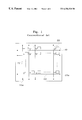
- a liquid crystal display device includes a TFT array substrate.
- a plurality of gate bus lines 60 are arranged horizontally and are spaced from each other by a certain distance.
- a plurality of data bus lines 70 are arranged vertically and are spaced from each other by a certain distance.
- the gate bus lines 60 and the data bus lines 70 are arranged so that the data bus lines 70 and the gate bus lines 60 intersect each other so as to define a matrix array.
- a gate pad 60 a and a data pad 70 a which are in contact with a drive IC are defined at the end of the gate bus line 60 and the data bus line 70 .
- a pixel electrode 40 is defined in each block area defined by the intersections of the gate bus line 60 and the data bus line 70 and a TFT 50 is also defined at the intersection point of the gate bus line 60 and the data bus line 70 .
- the TFT 50 includes a gate electrode 60 b which is made from material used to form the gate bus line 60 , a source electrode 70 b and a drain electrode 70 c which are made from a material used to form the data bus line 70 , and a semiconductor layer 90 .
- the drain electrode 70 c of the TFT is in contact with the pixel electrode 40 .
- a display device that is manufactured by simultaneously defining a gate bus line and a data bus line is suitable when forming a large LCD with the above-mentioned structure, which has more than a 14 or 15 inch display area.
- the size of an area that can be exposed at one time is limited. For example, for large panels, a one-shot exposing process cannot be used since the panel is too large for conventional exposing equipment.
- a divided exposure method is used.
- a first portion of a substrate is exposed first and then a second, remaining part of the substrate is exposed.
- using the divided exposure method results in a difference in line width at a boundary line between the first area exposed by the first exposing step and the second area exposed by the second exposure step.
- this difference in line width causes a difference in the resistance in the lines, which causes differences in luminance in the display. This luminance difference is called a stitching defect.
- a metal layer 55 in which a desired pattern is to be defined is disposed on a transparent substrate 10 using the divided exposure method.
- the area of the photo resist layer is divided into part A and part B.
- An exposure mask 100 which exposes part A of the photo resist layer 80 and a border line D that divides parts A and B are located in the same position.
- the exposure mask 100 includes an exposure pattern 150 which is used to patter part A of the photo resist layer [of part A] of the substrate 11 into a certain pattern and a light blocking member 140 .
- a light such as a UV ray which radiates from an exposure device on the exposure mask 100 penetrates the exposure pattern 150 and exposes the photo resist of part A of the substrate 11 with a certain pattern.
- an exposure mask 200 is located to be aligned with the border line D in order to expose part B of the photo resist layer 80 after eliminating the prior exposure mask 100 as shown in FIG. 3 b .
- the exposure mask 200 includes an exposure pattern 151 and a light blocking member 141 in order to exposure part B of the photo resist layer 80 of the substrate 11 .
- a light such as a UV ray which radiates from an exposure device on the exposure mask 200 penetrates the exposure pattern 151 and exposes the photo resist of part B of the substrate 11 with a certain pattern so at the end parts A and B which are divided by the border line D of the exposure mask are exposed into a certain pattern.
- the photo resist layer 80 is developed and while using the developed photo resist pattern layer as a mask, a lower metal layer 55 is etched to define a data bus line 70 and a drain electrode 70 c having a structure as shown in FIG. 4.
- a width (a) of a line such as the data bus line 70 which is located at the border part D of the divided exposure, is formed differently from widths (b) and (c) of the data bus lines 70 that are directly adjacent to the dividing line D as shown in FIGS. 4 and 5.
- the reason for the difference in the width pattern of the line formed at the border part of the divided exposure is because a metal layer is etched along the pattern of the photo resist.
- the rest of the photo resist is exposed in a state in which the location of the pattern of the exposure mask is slightly out of place or misaligned due to an error in positioning of the mask and the metal layer is etched according to such a pattern of the photo resist.
- the patterned width (a) of the data bus line 70 at the border part D of the divided exposure is wider than the widths (b) and (c) of the data bus lines 70 which are directly adjacent to the dividing line D if the exposure mask 200 is placed to the right of line D as shown in FIG. 4 .
- the patterned width (a) of the data bus line 70 at the border part D of the divided exposure is narrower than the widths (b) and (c) of the data bus lines 70 that are directly adjacent to the dividing line D if the exposure mask 200 is placed to the left of line D as shown in FIG. 5 .
- the substrate 11 of an LCD apparatus includes the pixel electrode 40 in contact with the drain electrode 70 c .
- the TFT is formed such that the data bus line 70 is formed in the above described manner.
- the stitching defect is identified by a difference in the resistance value of each line and this difference in resistance is due to the fact that the width (a) of the data bus line 70 at the border part D of the divided exposure is different from the widths (b) and (c) of the data bus lines 70 that are directly adjacent to the dividing line D. Therefore, when using the divided exposure method for making a large substrate, the occurrence of the stitching defect still cannot be avoided even though there is some improvement in the degree of occurrence compared to suing an exposure method which exposes a substrate using a one-shot exposure process.
- Preferred embodiments of the present invention overcome the problems of the conventional art described above by correcting the stitching defect which occurs at the border area of the divided exposure when the gate bus line and the data bus line are patterned using conventional divided exposure methods.
- a liquid crystal display includes a substrate, a plurality of gate lines disposed on the substrate, a plurality of data lines disposed on the substrate and arranged to define a matrix pattern with the plurality of gate lines, a plurality of thin film transistors connected to the gate lines and data lines, and a plurality of pixel electrodes connected to the thin film transistors, wherein a stitching defect correction element is included in at least one of the plurality of data lines.
- a method of a manufacturing liquid crystal display device includes the steps of forming a TFT array substrate in which a stitching defect correcting element is formed in between at least one of a plurality of data bus line and a data pad, and forming a wave shaped pattern with a width narrower than that of the data bus line at a selected stitching defect correcting element.
- FIG. 1 is a plane view of a conventional LCD apparatus
- FIG. 2 is a perspective view illustrating a portion of the LCD apparatus of FIG. 1;
- FIGS. 3 a and 3 d are cross-sectional views showing the process of line patterning of a substrate of an LCD apparatus using a divided exposure process
- FIG. 4 i a plan view showing a conventional LCD apparatus in which a line of a substrate is formed using a divided exposure method
- FIG. 5 is a plan view showing a conventional LCD apparatus in which a line of a substrate is formed using a divided exposure method
- FIG. 6 is a line pattern of a preferred embodiment of the present invention in which a stitching defect correcting element is defined
- FIG. 7 is a plan view showing a resistance pattern having a wave shape of a stitching defect correcting element according to a preferred embodiment of the present invention.
- FIG. 8 is a plan view showing a resistance pattern having a wave shape of a stitching defect correcting element according to a preferred embodiment of the present invention.
- a liquid crystal display device includes a stitching defect correcting element defined on at least one of the plurality of data bus lines or on at least one of the plurality of gate bus lines.
- the stitching defect correcting element includes a resistance changing element that has an increased thickness relative to the data bus line or the gate bus line.
- the resistance of the stitching defect correcting element can be changed or controlled by patterning it to define a wave shaped pattern in the stitching defect correcting element.
- the location of the stitching defect correcting element on the data line or the gate line is between an end of the respective line and the pad.
- a method of manufacturing the LCD structure as described above includes the steps of forming a TFT array structure in which at least one stitching defect correcting element is formed in between the plurality of the data bus line and the data pads and/or in between the plurality of the gate bus lines and the gate pads, and patterning the stitching defect correcting element to have wave shaped pattern using a laser.
- the TFT array substrate is formed such that a first metal layer is patterned using a divided exposure method whereby a stitching defect correcting element 85 is defined at a lower end of the gate pad 60 a and the gate bus line 60 is defined at an end of the stitching defect correcting element 85 .
- a second metal layer which is formed on the insulating layer with the divided exposure method is patterned so that the stitching defect correcting element 85 is at a lower end of the data pad 70 a .
- the gate bus line 60 and the data bus line 70 are described as if there is only one of each, however, a plurality of gate bus lines 60 are formed parallel to each other and a plurality of data bus lines 70 are formed to be parallel to each other and the gate bus lines 60 and the data bus lines 70 intersect each other.
- the stitching defect correcting element 85 does not need to be formed at each of the gate bus lines 60 or at each of the data bus lines 70 . It is sufficient to form the stitching defect correcting element only at one data bus line or one gate line disposed at the border part of the divided exposure, or to form a stitching defect correcting element at the data bus lines or gate bus lines which are within a certain area located to the left and right of the border part of the dividing exposure.
- an electromagnetic sensor is used to sense the luminance of each pixel electrode to check for the stitching defect.
- the sensor senses each pixel electrode to determine the charge therein to determine any differences in luminance of the various pixel electrodes.
- width (a) of the data bus line 70 located at the border part D of the divided exposure is wider than widths (b) and (c) of the data bus lines 70 which are directly adjacent to the dividing line D.
- width (a) of the data bus line 70 located at the border part D of the divided exposure is narrower than widths (b) and (c) of the data bus lines 70 located directly adjacent to the dividing line D as shown in FIG. 8 .
- the luminance of the pixel electrode connected to the data bus line 70 which has a width (a) is different from the luminance of the pixel electrode connected to the data bus line 70 which has widths (b) and (c) when the luminance of the pixel electrode is checked.
- the area where this difference in luminance occurs is recognized as the stitching defect.
- the reason for this stitching defect is the difference in boundary current of the electrical charge of the pixel electrode due to the difference in flow of voltage in the data bus line as the resistance value of the data bus line 70 which has a width (a) is lower than that of the data bus lines 70 which has widths (b) and (c).
- the resistance value of the data bus line 70 having a width (a) is greater than that of the data bus lines 70 which have widths (b) and (c) so, the stitching defect is not avoidable unlike the situation in FIG. 7 .
- the above-described problems of stitching defects caused when using the divided exposure method are solved by adjusting the flow of the resistance value.
- a wave shaped pattern is defined such that the recessed portions of the stitching correcting element width is narrower than that of the data bus line. Defining the wave shaped pattern on the stitching defect correcting element changes the resistance value in the data bus line so that the resistance value in the data bus line at the border part of the divided exposure is similar to the resistance value of the adjacent data bus lines.
- the resistance value is adjusted by defining a wave shaped resistance pattern having a width that is narrower than the data bus line at the stitching defect correcting element 85 which is connected to the data bus line.
- a wave shaped resistance pattern is formed to have a width that is narrower than the data bus lines at the adjacent stitching defect correcting element 85 of the data bus line 70 having widths (b) and (c).
- the wave shaped resistance pattern is formed using a laser by alternatively cutting both ends of the stitching defect correcting element. Because the width of each resistance pattern G 1 , G 2 , G 3 , G 4 . . . is narrower and because the number of the resistance patterns increases, the resistance value increases. Thus, by adjusting the number and width of the resistance patterns, the resistance value is adjusted.
- a stitching defect correcting element 85 may preferably be formed at an end of the gate pad part 60 a or the data pad part 70 a according to one preferred embodiment of the present invention. Because the stitching defect correcting element is formed by a pattern defining the stitching defect correcting element at the divided exposure mask, the stitching defect correcting element is patterned at the same time that the data bus line or the gate bus line is patterned. The stitching defect correcting element does not need to be formed at all of the gate bus lines or at all of the data bus lines. Forming the stitching defect correcting element at the data bus lines or gate bus lines which are within a certain area to the left and right of the border part of the divided exposure is sufficient to achieve the advantages of the present invention and to eliminate stitching defects.
- the advantages achieved by the present invention include eliminating stitching defects easily by forming resistance pattern G 1 , G 2 , G 3 , G 4 by alternatively cutting both ends of at least one stitching defect correcting element formed at an end of at least one of the data bus lines 70 or at least one of the gate bus lines 60 and which is connected to the gate bus line and the data bus line located new the border part.
Abstract
Description
Claims (32)
Priority Applications (1)
| Application Number | Priority Date | Filing Date | Title |
|---|---|---|---|
| US09/432,522 US6356320B1 (en) | 1999-11-03 | 1999-11-03 | LCD with TFT array having wave-shaped resistance pattern to correct stitching defect |
Applications Claiming Priority (1)
| Application Number | Priority Date | Filing Date | Title |
|---|---|---|---|
| US09/432,522 US6356320B1 (en) | 1999-11-03 | 1999-11-03 | LCD with TFT array having wave-shaped resistance pattern to correct stitching defect |
Publications (1)
| Publication Number | Publication Date |
|---|---|
| US6356320B1 true US6356320B1 (en) | 2002-03-12 |
Family
ID=23716519
Family Applications (1)
| Application Number | Title | Priority Date | Filing Date |
|---|---|---|---|
| US09/432,522 Expired - Lifetime US6356320B1 (en) | 1999-11-03 | 1999-11-03 | LCD with TFT array having wave-shaped resistance pattern to correct stitching defect |
Country Status (1)
| Country | Link |
|---|---|
| US (1) | US6356320B1 (en) |
Cited By (13)
| Publication number | Priority date | Publication date | Assignee | Title |
|---|---|---|---|---|
| US20020085169A1 (en) * | 2000-12-30 | 2002-07-04 | Choi Gyo Un | Liquid crystal display for testing defects of wiring in panel |
| US20030086048A1 (en) * | 2001-11-02 | 2003-05-08 | Nec Corporation | Liquid crystal display |
| US6665045B2 (en) * | 2000-03-28 | 2003-12-16 | Fujitsu Display Technologies Corporation | Liquid crystal display panel and method of manufacturing the same |
| WO2004042781A2 (en) * | 2002-11-05 | 2004-05-21 | Samsung Electronics Co., Ltd. | Thin film transistor array panel |
| US20040100605A1 (en) * | 2002-11-19 | 2004-05-27 | Nec Lcd Technologies, Ltd. | Liquid crystal display device and method of fabricating the same |
| US20040229410A1 (en) * | 2003-01-27 | 2004-11-18 | Fujitsu Display Technologies Corporation | Pattern forming method, method of manufacturing thin film transistor substrate, method of manufacturing liquid crystal display and exposure mask |
| CN100368876C (en) * | 2004-12-28 | 2008-02-13 | 中国电子科技集团公司第五十五研究所 | Active matrix liquid crystal display with special aspect ratio and laser cutting and manufacturing method therefor |
| CN100368878C (en) * | 2004-12-28 | 2008-02-13 | 中国电子科技集团公司第五十五研究所 | Nonstandard size active matrix liquid crystal display and grinding manufacturing method therefor |
| CN100368877C (en) * | 2004-12-28 | 2008-02-13 | 中国电子科技集团公司第五十五研究所 | Thin film transistor liquid crystal display and machine cutting and manufacturing method therefor |
| US20080044953A1 (en) * | 2006-07-03 | 2008-02-21 | Au Optronics Corp. | Method for forming an array substrate |
| US20090167972A1 (en) * | 2003-03-28 | 2009-07-02 | Jin Cheol Hong | Liquid crystal display device |
| US20130153936A1 (en) * | 2011-12-15 | 2013-06-20 | Panasonic Corporation | Device manufacturing method and organic el device |
| US9431381B2 (en) * | 2014-09-29 | 2016-08-30 | Taiwan Semiconductor Manufacturing Company, Ltd. | System and method of processing cutting layout and example switching circuit |
Citations (5)
| Publication number | Priority date | Publication date | Assignee | Title |
|---|---|---|---|---|
| US5026143A (en) * | 1985-02-06 | 1991-06-25 | Sharp Kabushiki Kaisha | Active type liquid crystal matrix display having signal electrodes with expanded sections at group exposure boundaries |
| US5656526A (en) * | 1993-12-07 | 1997-08-12 | Kabushiki Kaisha Toshiba | Method of fabricating a display device |
| US5714770A (en) * | 1995-12-05 | 1998-02-03 | Samsung Electronics Co., Ltd. | Thin film transistor substrate for a liquid crystal display |
| JPH10153791A (en) | 1996-11-25 | 1998-06-09 | Hitachi Ltd | Liquid crystal display device with bent wiring electrode |
| US6088073A (en) * | 1997-04-14 | 2000-07-11 | Casio Computer Co., Ltd. | Display device with destaticizing elements and an electrostatic pulse delaying element connected to each of the destaticizing elements |
-
1999
- 1999-11-03 US US09/432,522 patent/US6356320B1/en not_active Expired - Lifetime
Patent Citations (5)
| Publication number | Priority date | Publication date | Assignee | Title |
|---|---|---|---|---|
| US5026143A (en) * | 1985-02-06 | 1991-06-25 | Sharp Kabushiki Kaisha | Active type liquid crystal matrix display having signal electrodes with expanded sections at group exposure boundaries |
| US5656526A (en) * | 1993-12-07 | 1997-08-12 | Kabushiki Kaisha Toshiba | Method of fabricating a display device |
| US5714770A (en) * | 1995-12-05 | 1998-02-03 | Samsung Electronics Co., Ltd. | Thin film transistor substrate for a liquid crystal display |
| JPH10153791A (en) | 1996-11-25 | 1998-06-09 | Hitachi Ltd | Liquid crystal display device with bent wiring electrode |
| US6088073A (en) * | 1997-04-14 | 2000-07-11 | Casio Computer Co., Ltd. | Display device with destaticizing elements and an electrostatic pulse delaying element connected to each of the destaticizing elements |
Cited By (32)
| Publication number | Priority date | Publication date | Assignee | Title |
|---|---|---|---|---|
| US6665045B2 (en) * | 2000-03-28 | 2003-12-16 | Fujitsu Display Technologies Corporation | Liquid crystal display panel and method of manufacturing the same |
| US20020085169A1 (en) * | 2000-12-30 | 2002-07-04 | Choi Gyo Un | Liquid crystal display for testing defects of wiring in panel |
| US6999153B2 (en) * | 2000-12-30 | 2006-02-14 | Boe-Hydis Technology Co., Ltd. | Liquid crystal display for testing defects of wiring in panel |
| US20030086048A1 (en) * | 2001-11-02 | 2003-05-08 | Nec Corporation | Liquid crystal display |
| US6879367B2 (en) * | 2001-11-02 | 2005-04-12 | Nec Lcd Technologies, Ltd. | Terminals having meandering portions liquid crystal display including lead wires for connecting circuit wiring to connectional |
| US20060102902A1 (en) * | 2002-11-05 | 2006-05-18 | Su-Gyeong Lee | Thin film transistor array panel |
| WO2004042781A2 (en) * | 2002-11-05 | 2004-05-21 | Samsung Electronics Co., Ltd. | Thin film transistor array panel |
| WO2004042781A3 (en) * | 2002-11-05 | 2004-09-30 | Samsung Electronics Co Ltd | Thin film transistor array panel |
| US7164153B2 (en) | 2002-11-05 | 2007-01-16 | Samsung Electronics Co., Ltd. | Thin film transistor array panel |
| US20040100605A1 (en) * | 2002-11-19 | 2004-05-27 | Nec Lcd Technologies, Ltd. | Liquid crystal display device and method of fabricating the same |
| US20060209234A1 (en) * | 2002-11-19 | 2006-09-21 | Nec Lcd Technologies, Ltd | Liquid crystal display device and method of fabricating the same |
| US20060209249A1 (en) * | 2002-11-19 | 2006-09-21 | Nec Lcd Technologies, Ltd | Liquid crystal display device and method of fabricating the same |
| US7136120B2 (en) * | 2002-11-19 | 2006-11-14 | Nec Lcd Technologies, Ltd. | Liquid crystal display device and method of fabricating the same |
| US7388644B2 (en) | 2002-11-19 | 2008-06-17 | Nec Lcd Technologies, Ltd. | Liquid crystal display device and method of fabricating the same |
| US7405782B2 (en) | 2002-11-19 | 2008-07-29 | Nec Lcd Technologies, Ltd. | Liquid crystal display device and method fabricating the same |
| US20040229410A1 (en) * | 2003-01-27 | 2004-11-18 | Fujitsu Display Technologies Corporation | Pattern forming method, method of manufacturing thin film transistor substrate, method of manufacturing liquid crystal display and exposure mask |
| US7279257B2 (en) * | 2003-01-27 | 2007-10-09 | Sharp Kabushiki Kaisha | Pattern forming method, method of manufacturing thin film transistor substrate, method of manufacturing liquid crystal display and exposure mask |
| US8279364B2 (en) * | 2003-03-28 | 2012-10-02 | Lg Display Co., Ltd. | Liquid crystal display device |
| US20090167972A1 (en) * | 2003-03-28 | 2009-07-02 | Jin Cheol Hong | Liquid crystal display device |
| CN100368878C (en) * | 2004-12-28 | 2008-02-13 | 中国电子科技集团公司第五十五研究所 | Nonstandard size active matrix liquid crystal display and grinding manufacturing method therefor |
| CN100368877C (en) * | 2004-12-28 | 2008-02-13 | 中国电子科技集团公司第五十五研究所 | Thin film transistor liquid crystal display and machine cutting and manufacturing method therefor |
| CN100368876C (en) * | 2004-12-28 | 2008-02-13 | 中国电子科技集团公司第五十五研究所 | Active matrix liquid crystal display with special aspect ratio and laser cutting and manufacturing method therefor |
| US20080044953A1 (en) * | 2006-07-03 | 2008-02-21 | Au Optronics Corp. | Method for forming an array substrate |
| US7547590B2 (en) | 2006-07-03 | 2009-06-16 | Au Optronics Corp. | Method for forming an array substrate including forming a transparent conductive layer on a photoresist and laser ablating |
| US20130153936A1 (en) * | 2011-12-15 | 2013-06-20 | Panasonic Corporation | Device manufacturing method and organic el device |
| CN103262653A (en) * | 2011-12-15 | 2013-08-21 | 松下电器产业株式会社 | Device manufacturing method, and organic el device |
| US8883530B2 (en) * | 2011-12-15 | 2014-11-11 | Panasonic Corporation | Device manufacturing method and organic EL device |
| CN103262653B (en) * | 2011-12-15 | 2017-06-16 | 株式会社日本有机雷特显示器 | The manufacture method and organic EL device of device |
| US9431381B2 (en) * | 2014-09-29 | 2016-08-30 | Taiwan Semiconductor Manufacturing Company, Ltd. | System and method of processing cutting layout and example switching circuit |
| US10522527B2 (en) | 2014-09-29 | 2019-12-31 | Taiwan Semiconductor Manufacturing Company, Ltd. | System and method of processing cutting layout and example switching circuit |
| US11024622B2 (en) | 2014-09-29 | 2021-06-01 | Taiwan Semiconductor Manufacturing Company, Ltd. | Integrated circuit having angled conductive feature |
| US11631661B2 (en) | 2014-09-29 | 2023-04-18 | Taiwan Semiconductor Manufacturing Company, Ltd. | Integrated circuit having angled conductive feature |
Similar Documents
| Publication | Publication Date | Title |
|---|---|---|
| US6304308B1 (en) | Liquid crystal display device with optical shield film | |
| KR100816333B1 (en) | Color filter plate and thin film transistor plate for liquid crystal display, and methods for fabricating the plates | |
| US6356320B1 (en) | LCD with TFT array having wave-shaped resistance pattern to correct stitching defect | |
| US7095458B2 (en) | Identification mark portion in liquid crystal display panel and fabricating method thereof | |
| KR100502797B1 (en) | Liquid crystal display device and manufacturing method thereof | |
| KR100315911B1 (en) | Liquid crystal display panel, method for fabricating the same and method for aligning the same | |
| US20060204863A1 (en) | Mask for light exposure | |
| US6929888B2 (en) | Photomask and exposure method for large scaled LCD device | |
| KR100312260B1 (en) | An LCD and a fabricating method thereof | |
| US6819399B2 (en) | Exposure mask for fabricating liquid crystal display and method for exposing substrate in fabricating liquid crystal display using the mask | |
| JP2005107504A (en) | Exposure mask, exposure apparatus comprising the same, and method for manufacturing display plate for display apparatus using the same | |
| US5956104A (en) | Active matrix-type liquid crystal display device and method of making the same | |
| US6291136B1 (en) | Method of manufacturing a liquid crystal display | |
| US6979604B2 (en) | Method for forming pattern on substrate and method for fabricating liquid crystal display using the same | |
| US7279257B2 (en) | Pattern forming method, method of manufacturing thin film transistor substrate, method of manufacturing liquid crystal display and exposure mask | |
| JPH04294329A (en) | Liquid crystal display device | |
| JP4221074B2 (en) | Manufacturing method of liquid crystal display device | |
| KR100301662B1 (en) | Liguid Crystal Display and Method Of Fabricating | |
| US20050110940A1 (en) | Method of manufacturing panel for liquid crystal display by division exposure | |
| US6653177B2 (en) | Patterning method, thin film transistor matrix substrate manufacturing method, and exposure mask | |
| JPH0728074A (en) | Display device and its production | |
| JPH1020341A (en) | Liquid crystal display device and its production | |
| KR20050060669A (en) | Manufacturing method of thin film transistor array panel | |
| KR100590754B1 (en) | Manufacturing method of thin film transistor substrate for liquid crystal display | |
| KR20020090430A (en) | Manufacturing method of thin film transistor substrate for liquid crystal display |
Legal Events
| Date | Code | Title | Description |
|---|---|---|---|
| AS | Assignment |
Owner name: LG. PHILIPS LCD CO., LTD., KOREA, REPUBLIC OF Free format text: ASSIGNMENT OF ASSIGNORS INTEREST;ASSIGNORS:CHUNG, IN JAE;CHOO, KYO SEOP;REEL/FRAME:010587/0336 Effective date: 20000124 |
|
| STCF | Information on status: patent grant |
Free format text: PATENTED CASE |
|
| FEPP | Fee payment procedure |
Free format text: PAYOR NUMBER ASSIGNED (ORIGINAL EVENT CODE: ASPN); ENTITY STATUS OF PATENT OWNER: LARGE ENTITY |
|
| FPAY | Fee payment |
Year of fee payment: 4 |
|
| AS | Assignment |
Owner name: LG DISPLAY CO., LTD., KOREA, REPUBLIC OF Free format text: CHANGE OF NAME;ASSIGNOR:LG.PHILIPS LCD CO., LTD.;REEL/FRAME:020985/0675 Effective date: 20080304 Owner name: LG DISPLAY CO., LTD.,KOREA, REPUBLIC OF Free format text: CHANGE OF NAME;ASSIGNOR:LG.PHILIPS LCD CO., LTD.;REEL/FRAME:020985/0675 Effective date: 20080304 |
|
| FPAY | Fee payment |
Year of fee payment: 8 |
|
| FEPP | Fee payment procedure |
Free format text: PAYOR NUMBER ASSIGNED (ORIGINAL EVENT CODE: ASPN); ENTITY STATUS OF PATENT OWNER: LARGE ENTITY Free format text: PAYER NUMBER DE-ASSIGNED (ORIGINAL EVENT CODE: RMPN); ENTITY STATUS OF PATENT OWNER: LARGE ENTITY |
|
| FPAY | Fee payment |
Year of fee payment: 12 |