US6370130B1 - Spread spectrum communication system - Google Patents
Spread spectrum communication system Download PDFInfo
- Publication number
- US6370130B1 US6370130B1 US09/092,914 US9291498A US6370130B1 US 6370130 B1 US6370130 B1 US 6370130B1 US 9291498 A US9291498 A US 9291498A US 6370130 B1 US6370130 B1 US 6370130B1
- Authority
- US
- United States
- Prior art keywords
- signal
- input
- sampling
- outputs
- matched filters
- Prior art date
- Legal status (The legal status is an assumption and is not a legal conclusion. Google has not performed a legal analysis and makes no representation as to the accuracy of the status listed.)
- Expired - Fee Related
Links
Images


Classifications
-
- H—ELECTRICITY
- H04—ELECTRIC COMMUNICATION TECHNIQUE
- H04B—TRANSMISSION
- H04B1/00—Details of transmission systems, not covered by a single one of groups H04B3/00 - H04B13/00; Details of transmission systems not characterised by the medium used for transmission
- H04B1/69—Spread spectrum techniques
- H04B1/707—Spread spectrum techniques using direct sequence modulation
- H04B1/7073—Synchronisation aspects
- H04B1/7075—Synchronisation aspects with code phase acquisition
- H04B1/7077—Multi-step acquisition, e.g. multi-dwell, coarse-fine or validation
-
- H—ELECTRICITY
- H04—ELECTRIC COMMUNICATION TECHNIQUE
- H04B—TRANSMISSION
- H04B7/00—Radio transmission systems, i.e. using radiation field
- H04B7/24—Radio transmission systems, i.e. using radiation field for communication between two or more posts
- H04B7/26—Radio transmission systems, i.e. using radiation field for communication between two or more posts at least one of which is mobile
- H04B7/2628—Radio transmission systems, i.e. using radiation field for communication between two or more posts at least one of which is mobile using code-division multiple access [CDMA] or spread spectrum multiple access [SSMA]
-
- H—ELECTRICITY
- H04—ELECTRIC COMMUNICATION TECHNIQUE
- H04B—TRANSMISSION
- H04B1/00—Details of transmission systems, not covered by a single one of groups H04B3/00 - H04B13/00; Details of transmission systems not characterised by the medium used for transmission
- H04B1/69—Spread spectrum techniques
- H04B1/707—Spread spectrum techniques using direct sequence modulation
- H04B1/7073—Synchronisation aspects
- H04B1/70735—Code identification
-
- H—ELECTRICITY
- H04—ELECTRIC COMMUNICATION TECHNIQUE
- H04B—TRANSMISSION
- H04B1/00—Details of transmission systems, not covered by a single one of groups H04B3/00 - H04B13/00; Details of transmission systems not characterised by the medium used for transmission
- H04B1/69—Spread spectrum techniques
- H04B1/707—Spread spectrum techniques using direct sequence modulation
- H04B1/7073—Synchronisation aspects
- H04B1/7075—Synchronisation aspects with code phase acquisition
- H04B1/708—Parallel implementation
-
- H—ELECTRICITY
- H04—ELECTRIC COMMUNICATION TECHNIQUE
- H04B—TRANSMISSION
- H04B2201/00—Indexing scheme relating to details of transmission systems not covered by a single group of H04B3/00 - H04B13/00
- H04B2201/69—Orthogonal indexing scheme relating to spread spectrum techniques in general
- H04B2201/707—Orthogonal indexing scheme relating to spread spectrum techniques in general relating to direct sequence modulation
- H04B2201/70702—Intercell-related aspects
-
- H—ELECTRICITY
- H04—ELECTRIC COMMUNICATION TECHNIQUE
- H04B—TRANSMISSION
- H04B2201/00—Indexing scheme relating to details of transmission systems not covered by a single group of H04B3/00 - H04B13/00
- H04B2201/69—Orthogonal indexing scheme relating to spread spectrum techniques in general
- H04B2201/707—Orthogonal indexing scheme relating to spread spectrum techniques in general relating to direct sequence modulation
- H04B2201/70707—Efficiency-related aspects
- H04B2201/7071—Efficiency-related aspects with dynamic control of receiver resources
Definitions
- the present invention relates to a spread spectrum communication system.
- Spread spectrum communication systems have received attention due to their high frequency efficiency as the number of users of the land mobile communication steeply increases.
- the DS-CDMA cellular system is going to be standardized by an international committee on communication.
- the DS-CDMA system is classified into two types: strictly synchronous base stations and asynchronous base stations.
- the global positioning system (GPS) or other systems are used in the synchronous system for synchronization.
- the acquisition is easy for the synchronous system only by a synchronization of a long code which is common to every base station.
- Each base station has a delay time of the long code different from the delay times of other base stations.
- the peripheral cell search for the hand-over is quick because a mobile station receives a delay information from base stations.
- the initial cell (sector) search takes a longer time for the mobile station because it is necessary to identify a spreading code sequence. It takes a lot of time when the spreading code is long. However, the search time may be decreased by information on the spreading code from base stations of adjacent cells, and it is advantageous that synchronization by signals from satellites is unnecessary.
- a cell search method for quick acquisition in the asynchronous system is proposed in “Two-stage Rapid Long Code Acquisition Scheme in DS-CDMA Asynchronous Cellular System” by Kenichi HIGUCHI, Mamoru SAWAHASH 1 and Fumiyuki ADACHI, Technical Report of IEICE, CS96-19, RCS96-12(1996-05).
- Composite codes are generated by corresponding long codes LC0 to LCX for identifying base stations and short codes SC0 to SCY for identifying channels.
- the short codes are common in all the cells and the code SC0 is allocated to common control channel (perch channel).
- the mobile station despreads a first short code SC0 by a matched filter that detects the timing of the long code.
- the long codes are identified by the matched filter or a sliding correlator.
- the number of cells search is decreased to be (Length and Phase of spreading code) compared to the number of (Number of spread code length ⁇ Number of spread code phases) in the asynchronous system above.
- Multi-media communication is required for transmitting a plurality of signals of different transmission rates.
- a type of variable spread ratio and a parallel multi-code type are proposed. Fading compensation is indispensable for these systems for high quality service.
- FIG. 47 shows a conventional receiver of a DS-CDMA system having a receiver antenna 101 for receiving a spread spectrum signal, a high frequency receiving portion 102 for converting the spread spectrum signal into an intermediate frequency signal, a divider 103 for dividing the intermediate frequency signal into two signals which are input to multipliers 106 and 107 .
- a signal (cos ⁇ t) of the intermediate frequency is generated by an oscillator 104 to be input to the multiplier 106 .
- a signal from the oscillator 104 is shifted by ⁇ /2 by a phase shifter 105 and is input to the multiplier 107 .
- the multipliers 106 and 107 multiply the divided signals by the signal from 104 and 105 , respectively.
- the outputs from the multipliers 106 and 107 are passed through low-pass filters 108 and 109 so that the base band signal of an in-phase component (I-component) and a quadrature component (Q-component) is extracted.
- I-component in-phase component
- the I- and Q-components are multiplied at a complex matched filter 110 by PN code sequence supplied from a EN generator 111 so as to be despread.
- the despread components have a plurality of peaks.
- the despread I- and Q-components are processed successively by a delay detection circuit 112 , a signal level detector 114 and a phase correction portion 116 .
- the delay detection circuit 112 detects a signal of one path, for example the first path, of a plurality of paths and inputs the signal to a frame synchronization detector 113 .
- the received signal has a pilot symbol already-known and four symbols are included in a slot.
- the frame synchronization detector 113 judges whether the four symbols are identical to a predetermined delay pattern so as to detect the frame synchronization.
- the detector outputs a frame synchronization signal to the phase correction portion 116 .
- the level detection portion 114 detects the signal level of the I- and Q-components.
- the multi-path selection portion 115 selects a plurality of paths with higher power from the maximum power and outputs a signal to the phase correction portion.
- the phase correction portion 116 has a plurality of phase correction means corresponding to the number of multi-paths and a selector for inputting the despread I- and Q-components according to the signal from the portions 113 and 115 .
- the despread signal of the matched filter 110 is input through the selector at timing of the phase correction means so that the phase correction means performs fading compensation of the despread signal.
- FIG. 48 shows a receiver for a semi-direct conversion for a spread spectrum communication.
- the receiver has an antenna 200 for receiving a signal of a band-pass filter (BPF) 211 , a low noise amplifier (LNA) 212 and a frequency converter 213 for outputting a signal of intermediate frequency, fc, by mixing a local oscillation signal of frequency fL.
- the frequency fL is for example, a boundary frequency of a frequency band of the received signal.
- a DC offset is reduced but a frequency offset remains.
- the received signal is a spread spectrum signal
- despreading is performed after the direct conversion.
- the direct conversion is more useful for other systems such as PHS than spread spectrum communication systems.
- the output of the frequency conversion is in the frequency domain at the positive and negative side on the frequency coordinate.
- a channel of a frequency exists in the negative domain equal to the frequency of the signal to be received.
- These two signals are separated by a channel filter having a complex coefficient.
- the output of the converter 213 is quadrature detected and over-sampled, then transformed by a Hirbert transformation portion 215 .
- the output of I- and Q-components of the portion 215 is input to the channel filter 216 so that signals of adjacent channels are reduced and input to a demodulator 217 .
- the demodulated signal is reproduced to the data transmitted by a data decision portion 218 .
- the Hirbert transformation needs rather complicated circuit.
- the present invention solves the above-discussed conventional problems and has an object to provide a spread spectrum communication system capable of high speed cell search.
- the present invention has another object to provide a spread spectrum communication system applicable to multi-media communication.
- the present invention has another object to provide a spread spectrum communication system of high reception quality even during multi-path fading.
- the present invention has another object to provide a spread spectrum communication system capable of high speed frame synchronization.
- the present invention has another object to provide a semi-direct conversion receiver of a simple and small scale circuit.
- a receiver for receiving a traffic channel and a common control channel has a plurality of matched filters at least one of which is selectively available for the traffic or the common control channel.
- a plurality of matched filters are used for receiving the common control channel.
- a plurality of matched filters are used to receive traffic channels of both the current base station and the base stations in the adjacent cells.
- a quantizing circuit for quantizing an output of a matched filter
- a delay detection circuit is provided for performing the delay detection using the output of the quantizing circuit.
- An output of the delay detection circuit is successively stored in a plurality of delay circuits so as to be compared.
- an interference reduction circuit has a real input and imaginary input for receiving an output of a frequency conversion circuit and for receiving a “0” input, respectively.
- FIG. 1 is a block diagram of the first embodiment of a receiver for a D-CDMA cellular system.
- FIG. 2 is a block diagram of a path selection portion for a traffic channel.
- FIG. 3 is a block diagram of a phase correction portion for a traffic channel.
- FIG. 4 is a block diagram of a rake combiner for the traffic channel.
- FIG. 5 is a flow chart of the initial cell search in the receiver in FIG. 1 .
- FIG. 6 is a block diagram of a matched filter in the second embodiment of a receiver for a spread spectrum communication system.
- FIG. 7 is a block diagram of a register for controlling the matched filter.
- FIG. 8 is a block diagram of circuits following the matched filter and showing the matched filter.
- FIG. 9 shows an alternate embodiment of the A/D converter shown in FIG. 3 .
- FIG. 10 is a timing chart of the matched filter and the circuit following thereto.
- FIG. 11 is a block diagram of a calculation register for storing a spreading code sequence.
- FIG. 12 is a block diagram of a switch circuit of register multiplexerREG-MUX in FIG. 11
- FIG. 13 is a circuit diagram of one sampling and holding circuit in FIG. 1 .
- FIG. 14 is a circuit diagram of the switch shown in FIG. 6 .
- FIG. 15 is a circuit diagram of the multi-plexer shown in FIG. 6 .
- FIG. 16 is a block diagram of circuits for setting a spreading code sequence applicable for a long delay multi-pass signal.
- FIG. 17 is signal sequence during fading correction.
- FIG. 18 is a circuit diagram of an addition circuit shown in FIG. 6 .
- FIG. 19 is a block diagram of the third embodiment of a matched filter bank.
- FIG. 20 shows another matched filter bank.
- FIG. 21 is a conceptual diagram of a hierarchy of control for a fourth embodiment of a matched filter.
- FIG. 22 shows the fourth embodiment of the matched filter.
- FIG. 23 is a block diagram of a sampling and holding circuit of the matched filter in FIG. 22 .
- FIG. 24 is a timing chart showing refresh timing of the sampling and holding circuit in FIG. 23 .
- FIG. 25 is a timing chart showing a refresh timing of another sampling and holding circuit.
- FIG. 26 is a timing chart of clocks CLK 0 and CLK 1 in FIG. 22 .
- FIG. 27 is a block diagram of a shift register in FIG. 22 .
- FIG. 28 is a block diagram of an input switching circuit in FIG. 22 .
- FIG. 29 is a block diagram of the fifth embodiment of a receiver.
- FIG. 30 is a block diagram of a variation of a receiver.
- FIG. 31 is a block diagram of a delay circuit in the matched filter shown in FIG. 29 .
- FIG. 32 shows a variation of the circuit in FIG. 31 .
- FIG. 33 is a block diagram of the sixth embodiment of a receiver.
- FIG. 34 ( a ) is a block diagram showing the first embodiment of a frame synchronization detection circuit.
- FIG. 34 ( b ) is a block diagram showing the second embodiment of a frame synchronization detection circuit.
- FIG. 35 ( a ) is a block diagram showing the third embodiment of a frame synchronization detection circuit.
- FIG. 35 ( b ) is a block diagram showing the fourth embodiment of a frame synchronization detection circuit.
- FIG. 36 is a block diagram showing the fifth embodiment of a frame synchronization detection circuit.
- FIG. 37 is a block diagram showing the sixth embodiment of a frame synchronization detection circuit.
- FIG. 38 is a block diagram of the seventh embodiment of the receiver.
- FIG. 39 shows a wave form of a spectrum of signals, showing an input signal in FIG. 39 ( a ) and an intermediate signal in FIG. 39 ( b ).
- FIG. 40 is a block diagram of a complex coefficient filter.
- FIG. 41 shows an example of frequency response of the filter in FIG. 40 .
- FIG. 42 shows a frequency response of a cascaded filter.
- FIG. 43 shows an example of a spectrum of sampled intermediate signal in FIG. 39 ( b ).
- FIG. 44 shows a frequency response of seven stages cascaded filter.
- FIG. 45 shows a frequency response of six stages cascaded filter.
- FIG. 46 shows simulation data of input and output signals of a interference rejection filter, showing an input signal in FIG. 46 ( a ), an output signal of a seven stages cascaded filter in FIG. 46 ( b ) and an output signal of six stages cascaded filter in FIG. 46 ( c ).
- FIG. 47 shows a conventional circuit for frame synchronization detection.
- FIG. 48 is block diagram of a conventional semi-direct conversion receiver.
- FIG. 1 is a block diagram of the first embodiment of a receiver for a D-CDMA cellular system.
- the reference 11 designates a signal input terminal for receiving the first branch base band signal generated by a quadrature detection from a spread spectrum signal received by a receiver antenna for the first branch (not shown)
- the reference 12 designates an input signal terminal for receiving the second branch base band signal generated by a quadrature detection from the spread spectrum signal received by a receiver antenna for the second branch (not shown).
- An in-phase component (I-component) and a quadrature component (Q-component) of the base band signals of first and second branches are input from the input terminals 11 and 12 , respectively.
- the base band signals are selected by a plurality of selectors 131 to 13 N parallelly connected to the terminals 11 and 12 for alternatively selecting the first or second branch.
- the selected signal is input to matched filters 141 to 14 N corresponding to the selectors 131 to 13 N.
- Matched filters 141 to 14 N are complex matched filters for calculating correlation between the base band signal and a replica of a spreading code sequence so as to despread the base band signal.
- the replica is selected corresponding to the signal to be received from a list (not shown) of spreading code sequences, and set to a spread code register.
- the matched filters are of double sampling and have a variable a number of taps. The number is from 8 to 1024. Any matched filter of CCD type, SAW filter type or digital IC type are applicable, however an analog matched filter proposed by the present inventors is advantageous in electrical power consumption and calculation accuracy.
- a signal processing portion (not shown) generates a long code timing signal for the cell search and path selection signal for the rake combining.
- the matched filters 141 to 14 K are connected to a path selection portion 16 for the common control channel, matched filters 14 K+1 to 14 K+D are connected to a multiplexer 15 , and matched filters 14 K+D+1 to 14 N are connected to a path selection portion 20 for the traffic channel.
- the multiplexer 15 selectively passes the outputs of matched filters 14 K+1 to 14 K+D to the path selection portions 16 or 20 according to a control signal from the signal processing portion. At the initial cell search, the outputs from 14 K+1 to 14 K+D are input to the selection portion 16 , and otherwise to the selection portion 20 .
- the path selection portion 16 receives outputs from the matched filters 141 to 14 K and outputs from matched filters 14 K+1 to 14 K+D through the multiplexer 15 .
- the portion selects one or more paths according to a path selection signal generated from the signal processing portion above.
- the signal processing portion calculates the power of the correlation outputs from 141 to 14 K+D and selects A (integer not less than 1) of higher power for each base station from the received signals.
- the path selection portion 16 selects the outputs from 141 to 14 K+D to input the phase correction portion 17 according to the path selection signal.
- the phase correction portion 17 performs fading correction of the output of a plurality of paths from the path selection portion 16 according to the phase error signal detected in the received signal of the pilot channel.
- a rake combiner 18 for maximal ratio combining of the received signal of the paths corrected in phase by the phase correction portion 17 at the timing of the corresonding path. The combining is performed for the signals of each base station.
- the output of the rake combiner 18 is input through a parallel/serial converter (P/S converter) 19 to a signal processing portion (not shown) for a soft decision, a de-interleaving and error correction coding.
- P/S converter parallel/serial converter
- the path selection portion 20 for the traffic channel receives the correlation outputs of the matched filters 14 K+1 to 14 K+D and 14 K+D+1 to 14 N, and outputs the selected signals to the phase correction portions 211 to 21 M.
- the portions 211 to 21 M correspond to codes C 1 to CM of multi-code.
- the signal corrected by the portions 211 to 21 M are input to the rake combiners 221 to 22 M.
- the rake combiners 221 to 22 M perform maximal ratio combining of the received signal of the paths corrected in phase by the phase correction portions 211 to 21 M at the timing of the corresponding path. The combining is performed for the signals of each base station.
- the output of the rake combiners 221 to 22 M are input through a parallel/serial converter (P/S converter) 23 to a signal processing portion (not shown) for a soft decision, a de-interleaving and error correction coding.
- P/S converter parallel/serial converter
- FIG. 2 shows input and output signals of the path section portion 20 .
- the outputs of matched filter 14 K+1 to 14 N are input to the portion 20 which selects a plurality of paths of higher signal power from the maximum power to the Ath power according to the path selection signal for each code.
- the phase correction portion 211 includes a plurality of phase correction means 301 to 30 A corresponding to the maximum to Ath paths.
- Each communication channel has a predetermined pilot signal of predetermined cycle.
- the phase correction value is obtained by detecting a phase of the pilot symbol.
- the received signal is multiplied by a conjugate complex of the phase error so as to be corrected in phase.
- a phase error prediction portion 321 calculates the phase error from the pilot symbol of the received signal so as to generate the phase corrected signal.
- a delay circuit 311 delays the received signal by a time equivalent to the process time of the phase error prediction portion 321 .
- a received signal is corrected in phase by multiplying the output of the delay circuit 311 in a multiplication circuit 331 by the phase correction signal of the prediction portion 321 .
- the phase correction means 302 to 30 A are similar to 301
- the phase correction portions 212 to 21 M are similar to 211 .
- the rake combiner 221 combines the multi-path signals of the received signal corrected in phase with code C 1 .
- the rake combiners 222 to 22 M combine the received signals of code C 2 to CM.
- the rake combiner 221 includes delay circuits 341 to 34 A and an adder 35 for adding outputs of the circuits 341 to 34 A.
- the rake combiners 222 to 22 M are similar to 221 .
- the outputs RAKEout_C 1 to REKEout_CM from the rake combiners 221 to 22 M are converted by a parallel to serial converter 23 ( FIG. 1) into a serial signal so as to be input to a signal processing portion.
- a plurality of matched filters are adaptively used according to the working condition for improving the cell search speed and the efficiency of multi-rate transfer.
- the total number N of matched filters, D, to be switched and the number M of multi-code filters are changeable.
- FIG. 5 is a flow chart of the initial cell search by the receiver.
- the multiplexer 15 is controlled so that the outputs of the matched filters 14 K+1 to 14 K+D are introduced to the path selection portion 16 .
- the initial cell search is performed by these matched filters.
- a common short code SC0 common to all of the cells is loaded to a PN register of the matched filter 141 .
- the first matched filter 141 calculates a correlation between received spread signal and the short code during one long code period.
- a maximum peak in the correlation is found so that a base station of a cell is identified to which the receiver (mobile station) belongs.
- An initial number “1” of a long code group number “i” is set in a counter (step S 13 ).
- Short codes GIC 1 to GICK+D are loaded to the spread code register of the matched filters 141 to 14 K+D, and the power outputs of the matched filters are compared with a predetermined threshold. When there is an output exceeding the threshold, a long code group is identified corresponding to the short code loaded in the matched filter (step S 14 ).
- step 15 an initial number “1” of a long code number “j” within the long code group “i” is set in a counter (step 15 ).
- a segment of “B” chips of the long codes LC(K+D)j ⁇ 1) to LC(k+D)j as the spread code replica included in the long code group are loaded (step 16 ).
- the matched filter 141 to 14 K+D calculate in parallel the correlation by the long codes.
- the signal processing portion stores the long code numbers and the power, and compares the power with a threshold (step 17 ).
- the long code number is taken as the long code number of the base station from which the signal is to be received step 20 ).
- the j in the counter is increased by “1” (step S 19 )
- the steps from S 16 are repeated until a long code is found higher than the threshold. Steps S 16 to S 19 b are repeated. If the step S 17 does not judge “Yes” with respect to codes up to the last code, the process is restarted from the step S 12 .
- a rapid initial cell search is possible by the parallel identification using K+D matched filters.
- the multi-plexer 15 is switched so as to feed the outputs of the matched filters 14 K+1 to 14 K+D to the path selection portion 20 .
- the processing portion for the common control channel receives only the outputs from the matched filters 141 to 14 K.
- the common control channel is received by the matched filters 141 to 14 K.
- the processing portion for the traffic channel receives the outputs from all other matched filters 14 K+1 to 14 N.
- the matched filters 14 K+1 and 14 K+2 are used if the diversity hand-over does not take place.
- the selectors 13 K+1 and 13 K+2 are switched so as to feed the received signal of the first antenna branch from the terminal 11 to the matched filter 14 K+1 and the received signal of the second antenna branch from the terminal 12 to the matched filter 14 K+2.
- the code C 1 is set as the spread code replica to the matched filters 14 K+1 and 14 K+2.
- Other matched filters 14 K+3 to 14 N are set to a sleep mode so that their electrical power consumption is decreased.
- the correlation outputs of the matched filters 14 K+1 and 14 K+2 are input through the multi-plexer 15 to the path selection portion 20 for the path selection. At most, a number of “A” paths are selected from the signals of two antenna branches.
- the received signals of the selected paths is input to the phase correction portion 211 corresponding to the code C 1 for phase correction, then combined by the rake combiner 221 .
- the output of the rake combiner 221 is input through the parallel serial converter to the signal processing portion.
- the phase correction portions 212 to 21 M and rake combiners 222 to 22 m are set to sleep mode.
- the hand-over of “two-site diversity hand-over” takes place.
- Information on the peripheral cells are transferred to the receiver in advance.
- the long codes of the base stations BS and BS 3 of the peripheral cells are set in the matched filters 141 to 14 K for peripheral cell search.
- a cell with maximum power is selected as the cell to be used next after the hand-over.
- the long code and short code of the next cell is loaded in the matched filters 14 K+3 and 14 K+4.
- the outputs of the matched filters 14 K+1 to 14 K+4 are input to the path selection portion 20 for the traffic channel.
- the phase correction portion 211 and the rake combiner 221 corresponding to the code C 1 perform phase correction and the rake combining.
- the output of rake combiner is input through the parallel serial converter to the signal processing portion.
- each of codes C 1 to CM are loaded to two matched filters.
- the selectors 131 to 13 N can be omitted when a plurality of sampling and holding circuits correspond to a plurality of antenna branches and to the matched filters 141 to 14 N.
- the outputs of the sampling and holding circuits are selectively input to the matched filters.
- the sampling and holding circuits in each matched filter is omitted to reduce the circuit size.
- FIGS. 6 to 18 show a second embodiment for the receiver.
- a matched filter for the diversity reception of two antenna branches includes two sampling and holding circuit groups SHG 1 and SHG 2 corresponding to signals Vb 1 and Vb 2 of the branches.
- SHGL and SHG 2 include a plurality of sampling and holding circuits SH 11 to SH 1 n and SH 21 to SH 2 n, respectively.
- SHG 1 and SHG 2 are commonly connected to a plurality of matched filters MUL 1 to MULm, which selectively read data of one of the groups. Since the matched filters are commonly used for the data of SHG 1 and SHG 2 , the circuit size is remarkably decreased.
- sampling and holding circuits of each group successively take data without transferring data between the sampling and holding circuits.
- the transfer error is prevented.
- a plurality of selectors SEL 11 to SEL 1 n are provided in the matched filter MUL 1 corresponding to the sampling and holding circuits in SHG 1 and SHG 2 .
- SEL 11 receives the outputs from SH 11 and SH 21 .
- SEL 11 selects one of these outputs.
- MULl includes a plurality of multi-plexers MUX 11 to MUX 1 ,n corresponding to the selectors SEL 11 to SEL 1 ,n, each for dividing the corresponding output of the selector into two outputs.
- the multi-plexers are controlled by the spread codes so as to switch the outputs.
- An adder ADD is connected to the outputs of the multi-plexers MUX 11 to MUX 1 ,n.
- the adder has two group inputs corresponding to each of the two outputs of the multi-plexers. In FIG. 6, these groups are designated by p (positive) and n(negative).
- An output of the adder ADD is input to a scaler (SCALER) for adjusting an output level.
- the matched filters MUL 2 to MULm are similar to MUL 1 .
- Vout 1 to Voutm are outputs of the matched filters MULl to MULm.
- FIG. 7 shows a register for controlling the matched filters.
- the sampling and holding circuits SH 11 to SH 1 n and SH 21 to SH 2 n are controlled by a shift register SMP which stores “n” number of one-bit data corresponding to SH 11 to SH 1 n and SH 21 to SH 2 n, respectively. These consists of one “1” and n ⁇ 1“0”.
- SMP circulates the bit “1” in a cycle of “n”.
- the sampling and holding circuits takes Vb 1 and Vb 2 when bit “1” is input.
- Wn has “n” bits of “1” corresponds to a spread ratio of “n” for outputting the total “n” outputs.
- W 4 has four bits of “1” and (n ⁇ 4) bits of “0” corresponds to a spread ratio of “4”. Data is output when the corresponding bit is “1”.
- FIG. 8 shows the circuits following the matched filters.
- the number of matched filters is “8” for easy understanding.
- Two matched filters MUL 01 and MUL 02 are for the perch channel group Pch (common control channel)
- four matched filters MUL 21 to MUL 24 are for the traffic channel group Tch
- two matched filters MUL 11 and MUL 12 are for a common channel Cch.
- Outputs of the groups Pch and Cch are input to multi-plexers MUXp 1 to MUXps of four inputs and one output.
- the multi-plexer MUXp 1 to MUXps selectively outputs one of the four outputs from MUL 01 , MUL 02 , MUL 11 and MUL 12 .
- Sampling and holding circuits SHp 1 to SHpS for multi-path are connected to the outputs of the multiplexers MUXp 1 to MUXps.
- SHp 1 to SHpS hold one of the peaks, respectively, occuring in Pch and Cch.
- An output of Pch is input to a peak detecting circuit PDp for sorting the power of the correlation outputs.
- a phase of peaks to be extracted is registered in PDp.
- PDp outputs a control signal for SHp 1 to SHpS which is decoded by a decoder DECp is sampling signals of the sampling and holding circuits. The detection and selection of the peaks
- the six outputs of Tch and Cch are input to a multi-plexer MUXt 1 to MUXtR of six inputs and one output for selectively outputting outputs of MUL 21 , MUL 22 , MUL 23 , MUL 24 , MUL 11 and MUL 12 .
- Sampling and holding circuits SHt 1 to SHtR for multi-path are connected to the outputs of the multi-plexers MUXt 1 to MUXtR.
- SHt 1 to SHtR hold one of the peaks, respectively, which appear in Tch and Cch.
- Outputs of Tch and Cch are input to a peak detecting circuit PDt for sorting the power of the correlation outputs. A phase of peaks to be extracted is registered in PDt.
- PDt outputs a control signal for SHt 1 to SHtR which is decoded by a decoder DECt as a sampling signal of the sampling and holding circuits. The detection and selection of the peaks are performed for all of the
- Cch is applicable for both of Pch and Tch.
- Pch has 2 to 4 channels and Tch has 4 to 6 channels.
- A/D converters ADp 1 to ADpS and ADt 1 to ADtR are connected to SHp 1 to SHpS and SHt 1 to SHtR, respectively, where the analog outputs of the sampling and holding circuits are converted into digital signals.
- Outputs of ADp 1 to ADpS are input to a multi-plexer MUX 31 for multi-path, and outputs of ADt 1 to ADtR are input to a multi-plexer MUX 32 for multi-path.
- These multi-plexers MUX 31 and MUX 32 alternatively output the data of the sampling and holding circuits for time-division processing of the fading correction and rake combining.
- the circuit therefor is small in size due to the time-division processing.
- ADp 1 to ADpS can be substituted by one A/D converter used in a time-division manner.
- ADt 1 to ADtR can be also substituted by one A/D converter.
- MUX 31 successively inputs the correlation outputs at the phase of peak power in the perch channel to a memory MEM 31 .
- I- and Q- components of the outputs are corrected by a fading correction circuit PC 31 .
- the signal is input to the rake combiner RCMB 31 and a rake combiner output Sout 1 is output.
- MUX 32 successively input the correlation outputs at the phase of peak power in the traffic channel to a memory MEM 32 .
- I- and Q-components of the outputs are corrected by a fading correction circuit PC 32 .
- the signal is input to the rake combiner RCMB 32 and a rake combiner output Sout 2 is output.
- FIG. 9 shows a variation of the A/D converter ADp 1 to ADpS and ADt 1 to ADtR.
- ADpI and ADpQ are connected through multiplexers pMUXI and pMUXQ to all the sampling and holding circuits SHp 1 to SHpS of the perch channel.
- ADtI and ADtQ are connected through multi-plexers tMUXI and tMUXQ to the total sampling and holding circuits SHt 1 to SHtR of the traffic channel.
- ADpI converts the I- component of SHp 1 to SHpS in a time-division manner.
- ADpQ converts the Q-component of SHp 1 to SHpS in time-division manner. The number of A/D converters is decreased by this embodiment.
- ADt 1 and ADtQ are similar to ADpI and ADpQ.
- FIG. 10 is a timing chart of the circuit in FIG. 8, showing the process by MUL 01 , MUL 02 , MUL 11 and MUL 12 for the perch channel. If five peaks of multi-path occur during one symbol period, five sampling and holding circuits among SHp 1 to SHpS are used. Here, the peaks are shown in the chart as “peak” and the sampling and holding timing is shown in the chart as “S/H”. The sampled data are successively stored in the memory MEM 31 as shown in the chart “memory”. The fading correction is performed after one symbol period, then the rake combining is performed further one symbol period delayed.
- the spread codes for the multi-plexers MUX 11 to MUX 1 n are stored in a calculation register CAL-REG for generating control signals CR 1 to CRn for the multi-plexers.
- the next codes are stored in an input register INP-REG.
- a switch circuit REG-MUX is used for transferring the code from INP-REG to CAL-REG. Code for one symbol is stored in INP-REG and the code is repeatedly reproduced in CAL-REG.
- the vertical lines are lines from INP-REG (at the bottom) to CAL-REG (at the top). The lines are designated by numbers 0 to 255.
- a multi-plexer 61 consisting of 128 two inputs and one output multiplexer is connected to the lines 128 to 255 .
- the multi-plexer MUX 61 introduces outputs 128 to 255 of INP-REG to inputs 128 to 255 of CAL-REG or introduces outputs 0 to 127 of INP-REG to inputs 128 to 255 of CAL-REG.
- When MUX 61 is connected to the outputs 0 to 127 of INP-REG, these outputs are input to the inputs 0 to 127 as well as 128 to 255 of CAL-REG.
- a multi-plexer 62 consisting of 64 two-input and one output multiplexer is connected to the lines 64 to 127 at a position nearer to INP-REG than MUX 61 .
- the multi-plexer MUX 62 introduces outputs 64 to 127 of INP-REG to inputs 64 to 127 of CAL-REG or introduces outputs 0 to 63 of INP-REG to inputs 64 to 127 of CAL-REG.
- the outputs 0 to 63 are input to the inputs 0 to 63, 64 to 127, 128 to 191 and 192 to 255 of CAL-REG.
- a multi-plexer 63 consisting of 32 two inputs and one output multiplexer is connected to the lines 32 to 63 at a position nearer to INP-REG than MUX 62 .
- the multi-plexer MUX 63 introduces outputs 32 to 63 of INP-REG to inputs 32 to 63 of CAL-REG or introduces outputs 0 to 31 of INP-REG to inputs 32 to 63 of CAL-REG.
- MUX 63 When MUX 63 is connected to the outputs 0 to 31, MUX 62 is connected to the outputs 0 to 63 and MUX 61 is connected to the outputs 0 to 127 of INP-REG, the outputs 0 to 31 are input to the inputs 0 to 31, 32 to 63, 64 to 95, 96 to 127, 128 to 159, 160 to 191, 192 to 223 and 224 to 255 of CAL-REG.
- a multi-plexer 64 consisting of 16 two inputs and one output multiplexer is connected to the lines 16 to 31 at a position nearer to INP-REG than MUX 63 .
- the multi-plexer MUX 64 introduces outputs 16 to 31 of INP-REG to inputs 16 to 31 of CAL-REG or introduces outputs 0 to 15 of INP-REG to inputs 16 to 31 of CAL-REG.
- the outputs 0 to 15 are input to the inputs 0 to 15, 16 to 31, 32 to 47, 48 to 63, 64 to 79, 80 to 95, 96 to 111, 112 to 127, 128 to 143, 144 to 159, 160 to 175, 176 to 191, 192 to 207, 208 to 223, 224 to 239 and 240 to 255 of CAL-REG.
- a multi-plexer 65 consisting of 8 two inputs and one output multiplexer is connected to the lines 8 to 15 at a position nearer to INP-REG than MUX 64 .
- the multi-plexer MUX 65 introduces outputs 8 to 15 of INP-REG to inputs 8 to 15 of CAL-REG or introduces outputs 0 to 7 of INP-REG to inputs 8 to 15 of CAL-REG.
- the outputs 0 to 7 are input to the inputs 0 to 7, 8 to 15, 16 to 23, 24 to 31, 32 to 39, 40 to 47, 48 to 55, 56 to 63, 64 to 71, 72 to 79, 80 to 87, 88 to 95, 96 to 103, 104 to 111, 112 to 119, 120 to 127, 128 to 135, 136 to 143, 144 to 151, 152 to 159, 160 to 167, 168 to 175, 176 to 183, 184 to 191, 192 to 199, 200 to 207, 208 to 215, 216 to 223, 224 to 231, 232 to 239, 240 to 247 and 248 to
- a multi-plexer 66 consisting of 4 two-input and one output multiplexer is connected to the lines 4 to 7 at a position nearer to INP-REG than MUX 65 .
- the multi-plexer MUX 66 introduces outputs 4 to 7 of INP-REG to inputs 4 to 7 of CAL-REG or introduces outputs 0 to 3 of INP-REG to inputs 4 to 7 of CAL-REG.
- the outputs 0 to 3 are input to the inputs 0 to 3, 4 to 7, 8 to 11, 12 to 15, 16 to 19, 20 to 23, 24 to 27, 28 to 31, 32 to 35, 36 to 39, 40 to 43, 44 to 47, 48 to 51, 52 to 55, 56 to 59, 60 to 63, 64 to 67, 68 to 71, 72 to 75, 76 to 79, 80 to 83, 84 to 87, 88 to 91, 92 to 95, 96 to 99, 100 to 103, 104 to 107, 108 to 111, 112 to 115, 116 to 119, 120 to 123, 124
- FIG. 13 shows that the sampling and holding circuit SH 1 has a switch SW 43 connected to an input voltage Vi 4 equivalent to the signals Vb 1 and Vb 2 .
- a input capacitance C 42 is connected to SW 43 , and an inverting amplifier INV 4 is connected to an output of the capacitance C 42 .
- An output of INV 4 is connected through a feedback capacitance C 41 to its input.
- SW 43 is switched from a closed position to an open position
- SH 1 holds Vi 4 .
- a refresh switch SW 42 is connected parallelly to C 41 to INV 4 , and a refresh switch SW 44 is connected to an input of C 42 for connecting a reference voltage Vref.
- Vref is equal to a threshold voltage of INV 4 and the input of INV 4 is always Vref.
- FIG. 14 shows the switch SW 41 having a transistor circuit T 5 consisting of pMOS and nMOS parallelly connected to an input voltage Vin 5 .
- a dummy transistor circuit DT 5 is connected to an output of T 5 consisting of pMOS and nMOS parallelly connected to T 5 and short-circuited at its input and output.
- a clock CLK 0 and its inversion by an inverter 15 are input to gates of T 5 and DT 5 as control signals.
- the control signal is inverted with respect to nMOS and pMOS of T 5 and DT 5 , and the relationship between control signal for T 5 and Dt 5 are inverted to each other.
- FIG. 15 shows the multi-plexer MUX 1 which includes multi-plexers MUX 91 and MUX 92 .
- MUX 91 consists of a pair of CMOS switches T 911 and T 912 connected to an input voltage Vin 9 ( the output of the sampling and holding circuit SH 1 ) and the reference voltage Vref, respectively.
- MUX 92 consists of a pair of CMOS switches T 922 and T 921 connected to an input voltage Vin 9 and the reference voltage Vref, respectively.
- the control signals for MUX 91 and MUX 92 are generated from a pre-control signal Pct.
- Pct is input to a buffer circuit consisting of buffers B 91 and B 92 and a delayed pre-control signal pct′ is generated.
- An input and output of the buffer circuit are input to a NOR gate G 91 and a AND gate G 92 .
- Outputs of G 91 and G 92 are input to inverter circuits I 91 and
- T 911 the output of G 91 is input to a gate of nMOS and the output of 191 is input to a gate of pMOS.
- T 912 the output of 192 is input to a gate of nMOS and the output of G 92 is input to a gate of pMOS.
- the first control signal ctl for introducing Vin 9 to an output Vop of positive side is generated from G 91 .
- the second control signal ct 2 for introducing Vref to an output Vop of positive side is generated from G 92 .
- the output of G 91 is input to a gate of pMOS and the output of I 91 is input to a gate of nMOS.
- the output of 192 is input to a gate of pMOS and the output of G 92 is input to a gate of nMOS.
- the first control signal ct 1 for introducing Vin 9 to an output Vom of negative side is generated from G 91 .
- the second control signal ct 2 for introducing Vref to an output Vom of negative side is generated from G 92 .
- FIG. 11 shows setting of a spread code while the multi-path delay exceeds one symbol period.
- a spread code PNk ⁇ 1 of (k ⁇ 1)th symbol period of a composite code is loaded to a calculation register CAL-REG 21
- a spread code PNk ⁇ 2 of (k ⁇ 2)th symbol period of a composite code is loaded to a calculation register CAL-REG 22 .
- One matched filter can detect a multi-path symbol with one symbol period. The detection of two symbol periods is possible by the two matched filters shown in FIG. 16 . The detection of longer periods is possible by more matched filters with spread codes successively delayed.
- FIG. 17 shows a received signal to be corrected for fading.
- the pilot symbols Pk, Pk+1, Pk+2, . . . are attached before data signals Sk, Sk+1, Sk+2 . . .
- An interpolation shown by a solid line is performed for fading correction.
- the extrapolation is performed by only one pilot symbol Pk before the data signal Sk, as shown by a broken line.
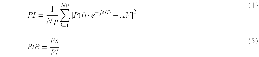
- the SIR is calculated as follows.
- the pilot symbol after the rake combining is shown in the formula (1), where
- n(i) component of noise and interference
- An averaged signal AV is calculated in the formula (2) by deleting modulation influence of the pilot symbol according to the fixed pilot symbol.
- I- and Q-components AVi and AVq are obtained as in the formula (2).
- the signal power Ps and interference power PI are obtained as in the formulae (3) and (4).
- SIR is a ratio of Ps and PI and is expressed by the formula (5).
- Ps
- 2 (AVi) 2 +(AVq) 2 (3)
- FIG. 18 shows the adder ADD having capacitances Cp 1 to Cpn fro receiving the positive inputs Vo 11 p to Vo 1 np and capacitances Cm 1 to Cmn for receiving the negative inputs Vo 11 m to Vo 1 nm.
- the first and second capacitive couplings are constructed by Cp 1 to Cpn and Cm 1 to Cmn, respectively.
- An output of the first capacitive coupling is input to an inverter INV 71 having odd number of CMOS inverters serially connected.
- An output of INV 71 is connected through a feedback capacitance CF 71 to its input. INV 71 outputs an inversion of the output of the first capacitive coupling with good linearity.
- An output of the second capacitive coupling is input to an inverter INV 72 having odd number of CMOS inverters serially connected.
- An output of INV 72 is connected through a feedback capacitance CF 72 to its input.
- INV 72 outputs an inversion of the output of the second capacitive coupling with good linearity.
- INV 71 The output of INV 71 is connected through an intermediate capacitance CC 7 to the input of INV 72 .
- INV 72 integrates the inversion of the outputs of the first capacitive coupling and the output of the second capacitive coupling.
- FIG. 19 shows a matched filter bank of the third embodiment.
- the reference designates an analog signal input terminal for receiving a base band signal obtained from a signal received from an antenna.
- the reference 12 designates a group of sampling and holding circuits SH 1 to SH 256 which are parallelly connected to the terminal 11 .
- the sampling and holding circuits are controlled by a control signal shown by “0” and “1” at the upper adjacent area of the sampling and holding circuits in FIG. 19 .
- the control signal is “1”
- the sampling and holding circuit takes new data.
- the control signal is shifted in response to a sampling clock CL.
- the initial condition of the control signal for SH 1 is “1” and SH 1 takes the analog signal from the terminal 11 .
- the control signal for SH 2 is “1” and for others are “0”, so SH 2 takes the signal.
- SH 3 , SH 4 , . . . take the signal successively.
- the sampling cycle from SH 1 is restarted.
- the reference 13 designates a PN code register for storing PN 1 to PN 256 of 256 chips.
- the register is a circulation type.
- the PN codes are shifted with circulation in response to a clock CL 1 synchronous to CL.
- the reference 141 to 14256 are multipliers for multiplying outputs from stages of the register 13 and outputs from SH 1 to SH 256 .
- PN codes in the register 13 are digital data and the multipliers 141 to 14256 are analog/digital multipliers.
- the reference 15 is an analog adder for summing the outputs of the multi-pliers 141 to 14256 up. A correlation between the received signal and the PN codes is calculated.
- the reference 16 is the second PN code register. This is a 256 stage shift register of the circulation type. Four chips PN code (PN′ 1 to PN′ 4 ) is repeatedly stored in the register 16 . The PN code is shifted by a shift clock CL 2 .
- the references 171 to 17256 designate multipliers for multiplying the input signal in the sampling and holding circuits by the PN codes in the register 16 .
- the reference 18 designates an addition control register of 256 stages. This is a shift register of circulation type. Four successive stages have data “1” and other stages have data “0”. The data are control signals for multi-plexers 201 to 20256 .
- the reference 19 designates a signal input terminal of a constant “0” for receiving a signal corresponding to “0” from an adder 21 .
- the multi-plexers 201 to 20256 selectively output the output of the multipliers 171 to 17256 or the signal corresponding to “0” controlled by the outputs from the register 18 . When the control signal is “1”, the output of the multipliers are selected, otherwise “ ⁇ ” is selected.
- the reference 21 designates an adder for outputting a correlation of 4 sampled date and 4 PN codes.
- sampling and holding circuits are commonly used for the matched filters for 256 chips and 4 chips and the circuit size becomes small.
- FIG. 20 shows another matched filter bank in which data is transferred between successive sampling and holding circuits one after another, 31 designates an analog signal input terminal and 32 designates an analog shift register for sampling the analog signal input from the terminal 31 and shifting the data in response to the clock CL. 33 designates the first PN register for storing the first PN codes of 256 chips from PN 1 to PN 256 . 341 to 34256 are multipliers for multiplying the data in the register 32 by PN 1 to PN 256 . 35 designates an adder for summing the outputs from the multipliers up.
- 38 designates an addition control register for controlling the multi-plexers 401 to 40256 .
- “1” is stored, and “0” is stored in other stages.
- 39 designates “0” input terminal, 401 to 40256 designate multi-plexers for selectively outputting the outputs of the multipliers or the “0” signal.
- FIG. 21 shows a hierarchy of a matched filter of the fourth embodiment.
- “RESET” is the top
- two system clocks “CLK 0 ” and “CLK 1 ” and “PN-CODE” are the second.
- the third is “TAP NUMBER CONTROL”
- the fourth includes “CACULATION MODE” and “SHORT-CODE AND LONG-CODE”.
- the fifth is “SLEEP CONTROL” and the sixth is “REFRESH CONTROL”.
- the upper layer is superior to the lower.
- a circuit of a sleep mode is not necessary to be refreshed. It means that “SLEEP CONTROL” is superior to “REFRESH CONTROL”. “TAP NUMBER CONTROL” is superior to both of “SLEEP CONTROL” and “REFRESH CONTROL”.
- the hierarchy makes the control system simple and the circuit size small.
- the sampling and holding circuit and addition circuit work intermittently and is in sleep mode most of time.
- FIG. 22 shows a matched filter having the hierarchy in FIG. 21 .
- a clock generating circuit for generating clocks CLK 0 and CLK 1 inverted to each other.
- CLK 0 is a system clock for the total system of the matched filter.
- CLK 1 is a sampling signal of intermediate timing of CLK 0 for a double sampling.
- CLK 0 is input to a sleep control circuit SLPCNT and to a refresh control circuit REFCNT. These circuits perform periodically sleep and refresh of circuits based on the clock CLK 0 .
- CLK 0 and CLK 1 are input as timing signals to the sampling and holding circuit SH for receiving an input signal Vin.
- the sampling and holding circuit SH holds the input signal successively and multiplies the signal by a PN code sequence.
- a short code PNS and a long code PNL as the PN code sequence.
- PNS is supplied from a short code register SCREG and PNL is supplied from a long code register LCREG.
- the PN code sequences are input through a input switching circuit INSW to a shift register SREG.
- the shift register SREG has a plurality of feedback outputs IR 1 , IR 2 , . . . , IRn at the intermediate stages and the last stage.
- the sampling and holding circuit receives the total data in the shift register so that the multiplication is controlled.
- the outputs of the sampling and holding circuit SH are input to an adder ADD which sums both of the double sampling data up so as to generate addition results Vout 1 and Vout 2 .
- a tap number control signal TCNT is input to INSW which selects one of the feedback outputs IR 1 to IRn according to TCNT. The selected output is introduced to the input of the shift register. The circulation of PN code sequence of the predetermined number is executed.
- the sampling and holding circuit SH has the first and second groups G 1 and G 2 of sampling and holding circuits for receiving the analog input voltage Vin.
- G 1 consists of sampling and holding circuits SH 11 , SH 12 , . . . , SH 1 n and G 2 consists of sampling and holding circuits SH 21 , SH 22 , . . . , SH 2 n corresponding to each other. These groups are alternatively used.
- the sampling and holding circuits of the first group are successively refreshed in a cycle of (n+1) chip time.
- a sampling and holding circuit SH 1 a is provided so as to be used when one of the sampling and holding circuits SH 11 to SH 1 n refreshed. SH 1 a is refreshed when all of the SH 11 to SH 1 n are used.
- sampling and holding circuits of the second group are successively refreshed similarly to the first group.
- a sampling and holding circuit SH 2 a is provided for a refreshed sampling and holding circuit among SH 21 to SH 2 n.
- SH 2 a is refreshed when all of the SH 21 to SH 2 n are used.
- the refresh control is independent from the tap number control. Unused sampling and holding circuits are refreshed when the number of taps is decreased for simplifying the control.
- G 1 and G 2 have a timing based on CLK 0 and CLK 1 , respectively.
- CLK 0 and CLK 1 have a cycle of the chip time and are shifted by a half of the chip time from each other, as shown in FIG. 26 .
- the sampling and holding of Vin is performed by SH 11 , SH 21 , SH 12 , SH 22 , . . . , SH 1 n, SH 2 n on every 1 ⁇ 2 chip time.
- a plurality of multi-plexers MUX 11 to MUX 1 n and MUX 1 a corresponding to SH 11 to SH 1 n and SH 1 a ,and a plurality of multi-plexers MUX 21 to MUX 2 n and MUX 2 a corresponding to SH 21 to SH 2 n and SH 2 a are provided.
- the multi-plexer MUX 1 i outputs a positive output Vo 1 ip when the PN code is “1” and a negative output Vo 1 im when the PN code is “0”.
- FIG. 24 is a timing chart of the refresh timing when the total number of the sampling and holding circuits is “6” for easy understanding.
- the sampling and holding is performed at pulses of solid line and the refresh is performed at pulses of broken line.
- SH 11 is refreshed and is substituted by SH 1 a .
- the data held by SH 1 a is kept until the next sampling timing of SH 1 is finished, they SH 1 a is refreshed.
- SH 12 is refreshed just after the refreshment of SH 1 a , then a new data is held by SH 1 a .
- SH 13 and other sampling and holding circuits are used for sampling and refreshing.
- the refresh timing is the same as in FIG. 24 when the number of taps is decreased to “3” in spite of that the frequency of the sampling and holding is twice as in FIG. 24 . This simplifies the control.
- the number of sampling and holding circuits for substitution can be more for more frequent refreshment.
- FIG. 27 shows the shift register SREG, which consists of a plurality of small shift registers SR 91 , SR 92 , . . . , SR 9 k serially connected.
- the feedback outputs IR 1 , IR 2 , . . . , IRn are output from the registers SR 1 ,SR 2 , . . . , SRn, respectively.
- the shift register is rather simple.
- FIG. 28 shows INSW, which consists of a selector SEL 10 .
- the above PNS, PNL, TCNT, IR 1 to IRn are input to SEL 10 , and SEL 10 selectively outputs one of these inputs as an output DD 10 .
- FIG. 29 shows the fifth embodiment of the receiver.
- the received signal of the intermediate frequency Ain 1 is divided into I- and Q-components by the quadrature detection and passed through low-pass filters LPF 1 and LPF 2 , respectively.
- the I- and Q-components I and Q from LPF 1 and LPF 2 are input to a matched filter MF as well as to a plurality of delay circuits D 1 , D 2 , . . . , Dn.
- a plurality of sliding correlators SC 1 to SCn corresponding to D 1 to Dn are connected to outputs of the corresponding delay circuits, respectively.
- the initial acquisition and phase change detection of the multi-path are performed by MF in high speed.
- SC 1 to SCn perform data demodulation.
- the sliding correlators consume much less electrical power than the matched filters.
- the receiver has high performance of acquisition and phase change detection with low power consumption.
- An output of MF is input to a power calculation portion PC for calculating the power of the correlation output.
- the calculated power is recurrently integrated by a path detection portion PD fro a predetermined time length. A plurality of paths of higher power from the maximum power are selected.
- An output of PD is input to a correlation control portion CC which controls delay time of the delay circuits D 1 to Dn so that the selected signals are synchronized with one another for the rake combining by a rake combiner RAKE.
- RAKE outputs combined demodulated data Doi and Doq for I- and Q-components.
- the phase change is detected by MF, so any circuits such as a delay locked loop (DLL) for tracking are not necessary.
- DLL delay locked loop
- the circuit size and the electrical power consumption are minimized.
- a short code common to all the base stations and long codes for each base station independent from one another are defined. These code are demodulated by two stages despread and demodulation. A control channel is transmitted modulated only by the short code. The receiver detects the timing of the long code by despread of the short code. The long code acquisition becomes of high speed.
- a received signal RS after the low-pass filter is input to a switch SW which output RS to one of two outputs.
- the first output is input to a short code processing portion SP and the other is input to a plurality of long code processing portions LP 1 to LP 3 .
- LP 1 to LP 3 correspond to paths detected by MF, for example, LP 1 corresponds the path of maximum power, LP 2 corresponds the second power and LP 3 corresponds the third.
- the number of long code processing portions is determined by a predicted number of multi-paths.
- SP includes MF and a short code generating portion SG for calculating the correlation of RS with the short code and for detecting the long code timing used in the initial acquisition and peripheral cell search.
- LP 1 includes the sliding correlator SC and a long code generating portion LG for calculating the correlation of RS with the long code, that is, for despread.
- LP 2 and LP 3 are similar to LP 1 .
- the output of MF is input to a memory MEM for storing a plurality of powers of the output.
- the maximum of the power is detected by a maximum detecting portion MS output of which is input to LG.
- MS determines a timing of the correlation calculation between SC and RS and generation of the long code according to the cell search.
- the short code is composed with the long code by an exclusive-or gate G.
- An output of G is input to a multiplication portion M.
- An output of M is input to a integrator IND for accumulating the multiplication result.
- An output of IND is input to a square-law detector SLD.
- Outputs of SLDs of LP 1 to LP 3 are added by an adder ADD.
- An output ADD is input to a comparator COMP. Since the outputs of the correlation power of a plurality of the sliding correlators are integrated, the influence of noise is reduced and the judgment accuracy is improved.
- the output of MS is further input to a threshold determining portion TD and the comparator COMP compares the outputs from ADD and TD.
- the correlation power by the short code is compared with the threshold determined by TD. Since TD determines the threshold according to the detected power by SP, the threshold is appropriate. A proper long code synchronization is obtained.
- FIG. 31 shows the delay circuits and MF.
- MF which includes a plurality of sampling and holding circuits S 1 to SN serially connected for successively holding a digital input signal Din.
- Outputs d 1 to dN from S 1 to SN are introduced to a multiplier MUL as well as a plurality of delay circuits DL 1 to DLn.
- the delay circuits have N inputs one output multi-plexers MUX 1 to MUXn. Each of the multi-plexers selects one input so that the correlation peak of the sliding correlators are adjusted in phase.
- the matched filter and sliding correlators may be of analog type in stead of the above.
- the delay circuits are substituted by a memory MEM.
- the input signal Vi is successively input to predetermined areas in MEM.
- the oldest data is replaced by a new data.
- read-out address ADD 1 to ADDn corresponding to the delay are input to MEM.
- a timing signal is read out.
- the delay time is set by a more simple circuit.
- FIG. 33 shows the sixth embodiment.
- the input signal is not delayed, but PN code is delayed.
- PN code is stored in a PN code generator PNG consisting of a shift register the last stage of which is fed back to the first stage.
- the PN code PN 1 to PNN of all stages are parallelly output to multiplexers MUX 41 to MUX 4 n connected to SC 1 to SCn, respectively.
- MUX 41 to MUX 4 n selects the inputs so as to generate a correlation peak. Since the one generator PNG is commonly used by a plurality of sliding correlators, the circuit size is small.
- FIG. 34 ( a ) shows a frame synchronization circuit for a spread spectrum communication.
- 11 designates a one bit quantizing circuit for converting the I- and Q-components of the output of the complex matched filter into sign signals sgn(Di) and sgn(Dq). Then the analog despread signal is converted into a digital data of one bit.
- 12 designates a delay circuit for delaying an output of the circuit 11 by one symbol time.
- An output of the multiplication circuit 13 is input to a delay circuit 14 and transferred to the delay circuits 15 and 16 serially connected to the circuit 15 .
- the multiplication circuit 13 successively outputs a delay detection output of Pr( 1 ) and Pr( 2 ), Pr( 2 ) and Pr( 3 ), and Pr( 3 ) and Pr( 4 ).
- the delay circuits 16 , 15 and 14 output the delay detection outputs of of Pr( 1 ) and Pr( 2 ), Pr( 2 ) and Pr( 3 ), and Pr( 3 ) and Pr( 4 ). These delay detection outputs are input to multiplication circuits 17 to 19 .
- a theoretical delay detection pattern calculated from known pilot symbols is input to the multiplication circuits 17 to 19 .
- the known pilot symbol sequence is Po( 1 ), Po( 2 ), Po( 3 ) and Po( 4 )
- a multiplication of Po( 1 ) and a conjugate complex of Po( 2 ) is output from the multiplication circuit 19
- a multiplication of Po( 2 ) and a conjugate complex of Po( 3 ) is output from the multiplication circuit 18
- a multiplication of Po( 3 ) and a conjugate complex of Po( 4 ) is output from the multiplication circuit 17 .
- the outputs of the multiplication circuits 17 to 19 are added by adder 20 .
- An output of the adder is maximum when the delay detection is identical to the theoretical pattern. Practically, the output of the adder is compared with a threshold and is judged to be identical when the output is higher than the threshold.
- FIG. 34 ( b ) is an improvement of the embodiment in FIG. 34 ( a ).
- a delayed symbol is quantized to be one bit, while the non-delayed symbol remains as is.
- a calculation of formula (10) is executed by this embodiment and Xi and Xq of the formulae (11) and (12) are obtained.
- a symbol is successively delayed by delay circuits 21 to 24 .
- Outputs of the delay circuits 21 to 24 are input to multiplication circuits 25 to 28 , respectively.
- Outputs of the multiplication circuits 25 to 28 are added by an adder 29 and then input to an absolute circuit 30 .
- a despread signal Di+jDq is input to the delay circuit 21 , and a conjugate complex of a pilot symbol pattern is input to the multiplication circuits 25 to 28 .
- Di and Dq are expressed as in the formula (13) and (14). The formula (15) is obtained.
- FIG. 35 ( b ) shows the fourth embodiment in which thee outputs of the multiplication circuits 26 , 27 and 28 are subtracted from the outputs 25 , 26 and 27 , respectively, by subtracters 31 , 32 and 33 .
- the outputs of the subtracters 31 , 32 and 33 are input to absolute circuits 34 , 35 and 36 outputs of which are added by an adder 37 . If the phase of the successive symbol are equal to each other, the outputs from the subtracters 31 to 33 are zero as shown in the formula (17)
- FIG. 36 shows a circuit for performing frame synchronization.
- delay circuits 41 to 52 for 16 slots are serially connected.
- a plurality of multiplication circuits 61 to 72 corresponding to the delay circuits are connected to the corresponding delay circuits.
- the outputs of the multiplication circuits are added by an adder 73 .
- the output of the adder is input to an absolute circuit 74 .
- This embodiment is similar to the embodiment of FIG. 35 ( a ).
- the output of the absolute circuit 74 is expressed as in the formula (18).
- FIG. 36 ( b ) shows clock signal CLK input to the delay circuits 41 to 52 .
- the clock is synchronous to the pilot symbols P 1 to P 4 , P 5 to P 8 , . . . , P 13 to P 16 .
- FIG. 37 shows another circuit for the frame synchronization.
- delay circuits 41 to 52 for 16 slots are serially connected.
- a plurality of multiplication circuits 61 to 72 corresponding to the delay circuits are connected to the corresponding delay circuits.
- the outputs of the multiplication circuits of each slot are added using adders 81 , 82 , . . . , 86 .
- the output of the adders are input to respective absolute circuits 84 to 86 .
- the outputs of the absolute circuits are added by an adder 87 .
- the output of the adder 87 is as in the formula (19).
- FIG. 38 shows the seventh embodiment of the receiver having an antenna 10 , a band-pass filter (BPF) 11 and 14 , a low-noise amplifier (LNA) 12 , a frequency converter 13 , an interference filter of adjacent channel (ICF) 15 , a demodulator 16 and a data judgment portion 17 .
- the receiver is a type of semi-direct conversion.
- the frequency fL of the local oscillation signal input to the frequency converter 13 should be determined so that the interference component is not included.
- the difference fL has difference 3 B from the center frequency fo of the signal received by the antenna when the band width of the received signal is 2 B.
- the output of BPF 14 is input to a real input of ICF 15 , and the imaginary input of ICF 15 is grounded.
- the real and imaginary outputs are input to the demodulator 16 so that the I- and Q-components of the base band signal are obtained.
- the data judgment portion generates the data transmitted. Since the imaginary input of ICF 15 is “0”, a Hilbert transformation means can be omitted, and circuit is simplified.
- the interference filter of adjacent channel (ICF) 15 works as follows.
- the signal received by the antenna is expressed as in the formula (20).
- the center frequency of the interference wave is symmetrically distributed centering fo with constant frequency difference. Then, the formula (21) and (22) are given.
- FIG. 39 ( a ) is a spectrum of r(t) in the formula (24).
- the interference wave of the adjacent channel exists at the frequency of fo+2B and fo-2B.
- the frequency converter 13 outputs a intermediate frequency signal with a center frequency fc.
- the output of the frequency converter 13 passed through BPF 14 is as in the formula (26).
- the spectrum of r(t) of the formula (26) is shown in FIG. 39 ( b ).
- the signal to be received has a center frequency 3 B and the frequencies of the interference wave of the adjacent channel are B and 5 B.
- the real and imaginary inputs xI(t) and xQ(t) of ICF 15 are as in the formulae (27) and (28).
- ICF 15 is constructed by a plurality of serially connected notch filters.
- one notch filter consists of a sampling and holding circuit 20 , a delay circuit 21 connected to an output of the sampling and holding circuit, an addition circuit 23 connected to the circuit 20 parallel to the delay circuit 21 , and a multiplication circuit for multiplying an output of the circuit 21 by a complex multiplier “a” and for inputting a multiplication result to the adder 23 .
- the sampling cycle of the circuit 20 is T
- fs 1/T
- the channel interval is 2B x(t) is expressed by the formula (29).
- the multiplier “a” is as in the formula (30).
- An output y(t) is output from the adder 23 .
- the discrete x(t) and y(t) due to intermittent sampling are x(n) and y(n).
- X(f) and Y(f) are Fourier transformation of x(t) and y(t).
- the formula (31) is rewritten as below.
- Amplitude of the frequency response is a periodic function of a period of 1/T with a center frequency of one period and is given by formula (34).
- the null point of the frequency response is as in the formula (35).
- FIG. 41 shows one period of the frequency response of the notch filter.
- FIG. 42 shows cascaded notch filters for reducing a a lot of interference of adjacent channels.
- the frequency response is shown in the formulae (38) and (39).
- ⁇ i should be adjusted so that the null point frequency and center frequency are appropriate.
- the sampled signal has a frequency spectrum of FIG. 43 .
- the negative portion in FIG. 39 ( b ) is shown by broken arrows.
- ⁇ 11B is a symmetrical point of 5B
- 11B, 13B, 15B, and 17B are symmetrical points of ⁇ 5B, ⁇ 3B, ⁇ B and B.
- the output y(t) has only a component of e j2 ⁇ (3B)t (including I and Q) because ⁇ 3B of the signal to be received is also reduced as an interference.
- the frequency response of the example 4 of seven stages is shown in FIG. 44 .
- the examples 1 to 4, 6 and 7 of six stages may have frequency response without a reduced negative component.
- the components of real part COS(2 ⁇ (3B)) remains.
- the frequency response of one period is shown in FIG. 45 .
- FIG. 46 ( a ) is an input signal x(t)
- FIG. 46 ( c ) is a comparison data of the filter shown in FIG. 45 .
- An N stages cascaded filter has a Z transfer function of formula (40) which is expanded to be the formula (41).
Abstract
Description


| TABLE 1 |
| The followings are examples of cascaded notch filters. |
| EX. | θ | fc | fn | Interference to be Reduced |
| 1 | −3π/8 | −3B | −11B, 5B | −11B, |
| 2 | −π/8 | −B | −9B, 7B | −9B, |
| 3 | π/8 | B | −7B, 9B | −9B, |
| 4 | 3π/8 | 3B | −5B, 11B | −5B, |
| 5 | 5π/8 | 5B | −3B, 13B | −3B, 13B |
| 6 | 7π/8 | 7B | −B, 15B | −B, 15B |
| 7 | 9π/8 | 9B | B, 17B | B, 17B |

Claims (25)
Applications Claiming Priority (14)
| Application Number | Priority Date | Filing Date | Title |
|---|---|---|---|
| JP9-164919 | 1997-06-09 | ||
| JP16491997A JP3421541B2 (en) | 1997-06-09 | 1997-06-09 | Signal receiving apparatus and signal receiving method |
| JP9-184641 | 1997-06-26 | ||
| JP18464197A JP3278379B2 (en) | 1997-06-26 | 1997-06-26 | Frame synchronization detection circuit |
| JP27225197A JPH1198116A (en) | 1997-09-18 | 1997-09-18 | Receiver for cdma communication system |
| JP9-272251 | 1997-09-18 | ||
| JP29937797A JPH11122078A (en) | 1997-10-16 | 1997-10-16 | Matched filter |
| JP9-299377 | 1997-10-16 | ||
| JP9308096A JPH11127134A (en) | 1997-10-23 | 1997-10-23 | Signal receiver for ds-cdma cellular system |
| JP9-308096 | 1997-10-23 | ||
| JP32964697A JP3898315B2 (en) | 1997-11-14 | 1997-11-14 | Release material |
| JP9-329646 | 1997-11-14 | ||
| JP9-352472 | 1997-12-05 | ||
| JP9352472A JPH11177490A (en) | 1997-12-05 | 1997-12-05 | Cdma cellular system and signal receiving equipment |
Publications (1)
| Publication Number | Publication Date |
|---|---|
| US6370130B1 true US6370130B1 (en) | 2002-04-09 |
Family
ID=27566249
Family Applications (1)
| Application Number | Title | Priority Date | Filing Date |
|---|---|---|---|
| US09/092,914 Expired - Fee Related US6370130B1 (en) | 1997-06-09 | 1998-06-08 | Spread spectrum communication system |
Country Status (2)
| Country | Link |
|---|---|
| US (1) | US6370130B1 (en) |
| CN (1) | CN1202050A (en) |
Cited By (27)
| Publication number | Priority date | Publication date | Assignee | Title |
|---|---|---|---|---|
| US20010040915A1 (en) * | 1999-12-30 | 2001-11-15 | Ravi Subramanian | Configurable multimode despreader for spread spectrum applications |
| US20010046257A1 (en) * | 2000-04-28 | 2001-11-29 | Shoji Taniguchi | Synchronization establishing device, method of establishing synchronization, and receiver |
| EP1161111A1 (en) * | 2000-01-12 | 2001-12-05 | Mitsubishi Denki Kabushiki Kaisha | Mobile communication terminal and method of communication |
| US20020055357A1 (en) * | 2000-11-06 | 2002-05-09 | Ntt Docomo, Inc. | Mobile communication system in multi-carrier CDMA scheme using short code and long code |
| US20020191683A1 (en) * | 2000-11-27 | 2002-12-19 | Hans Cavander | Mobile communications device |
| US20030002569A1 (en) * | 2001-03-14 | 2003-01-02 | Oates John H. | Wireless communication systems and methods for long-code communications for regenerative multiple user detection involving implicit waveform subtraction |
| WO2003013040A1 (en) * | 2001-08-02 | 2003-02-13 | Morphics Technology, Inc. | Configurable terminal engine |
| US6621855B1 (en) * | 1999-05-26 | 2003-09-16 | Lockhead Martin Corporation | Scalable spread-spectrum signal detection and acquisition processor |
| US20030231702A1 (en) * | 2001-03-14 | 2003-12-18 | Oates John H. | Wireless communications systems and methods for cache enabled multiple processor based multiple user detection |
| US6678313B1 (en) * | 1998-12-25 | 2004-01-13 | Kokusai Electric Co., Ltd. | Correlation circuit for spread spectrum communication |
| US6707847B1 (en) | 1999-09-14 | 2004-03-16 | Nec Electronics Corporation | Method and apparatus for detecting a spread code from a perch channel |
| US20040091062A1 (en) * | 2000-05-12 | 2004-05-13 | Colmer Morgan James | Radio receiver |
| US6747969B1 (en) * | 1999-11-23 | 2004-06-08 | Olaf Hirsch | Transmission gap interference measurement |
| US20040137926A1 (en) * | 2002-12-31 | 2004-07-15 | Lg Electronics Inc. | Frequency searching method and apparatus in mobile communications |
| US20040190603A1 (en) * | 1999-02-25 | 2004-09-30 | Dabak Anand G. | Space time transmit diversity for TDD/WCDMA systems |
| US6807224B1 (en) * | 1999-02-09 | 2004-10-19 | Matsushita Electric Industrial Co., Ltd. | CDMA receiving apparatus and CDMA receiving method |
| US6816717B1 (en) * | 1999-03-30 | 2004-11-09 | Nokia Corporation | Estimation of signal to interference ratio in a mobile communication system |
| US20040258041A1 (en) * | 2003-06-17 | 2004-12-23 | Che-Li Lin | Cell search method suitable for initial cell search and target cell search |
| US20050123071A1 (en) * | 2002-07-30 | 2005-06-09 | Hiroki Okada | Digital signal processing and receiving apparatus and method |
| US20050143117A1 (en) * | 2003-12-31 | 2005-06-30 | Infineon Technologies Morphics, Inc. | Signal-to-interference ratio estimation for CDMA |
| US20050160304A1 (en) * | 2003-10-24 | 2005-07-21 | Matsushita Electric Industrial Co., Ltd. | Matched filter circuit and correlation calculation method |
| US20050169349A1 (en) * | 1999-08-17 | 2005-08-04 | Samsung Electronics Co., Ltd. | Method for communicating scrambling code ID in mobile communication system |
| US20050180376A1 (en) * | 2004-02-17 | 2005-08-18 | Texas Instruments Incorporated | Implementation for a 5 sample guard interval for multi-band OFDM |
| US20050249268A1 (en) * | 2004-05-05 | 2005-11-10 | Texas Instruments Incorporated | (Updated) preamble for FDMA |
| US20050265433A1 (en) * | 1999-04-02 | 2005-12-01 | Yukihiko Okumura | Channel estimation device and method, demodulation device and method, and fading frequency decision device and method |
| US20060245400A1 (en) * | 1997-06-16 | 2006-11-02 | Nec Corporation | High-speed cell search system for CDMA |
| US8494471B2 (en) | 2009-02-25 | 2013-07-23 | Mitsubishi Electric Corporation | Receiver |
Families Citing this family (3)
| Publication number | Priority date | Publication date | Assignee | Title |
|---|---|---|---|---|
| US7496069B2 (en) * | 2003-04-11 | 2009-02-24 | Motorola, Inc. | Method and apparatus for public long code mask handoff management |
| US7046753B2 (en) * | 2004-06-29 | 2006-05-16 | Provigent Ltd. | Interference canceller with fast phase adaptation |
| CN115396082B (en) * | 2022-07-26 | 2024-02-09 | 上海宇航系统工程研究所 | Method for resisting long-distance communication phase distortion for carrier rocket |
Citations (2)
| Publication number | Priority date | Publication date | Assignee | Title |
|---|---|---|---|---|
| US5790588A (en) * | 1995-06-07 | 1998-08-04 | Ntt Mobile Communications Network, Inc. | Spread spectrum transmitter and receiver employing composite spreading codes |
| US6038250A (en) * | 1997-01-07 | 2000-03-14 | Yozan Inc. | Initial synchronization method and receiver for DS-CDMA inter base station asynchronous cellular system |
-
1998
- 1998-06-08 CN CN98109592A patent/CN1202050A/en active Pending
- 1998-06-08 US US09/092,914 patent/US6370130B1/en not_active Expired - Fee Related
Patent Citations (3)
| Publication number | Priority date | Publication date | Assignee | Title |
|---|---|---|---|---|
| US5790588A (en) * | 1995-06-07 | 1998-08-04 | Ntt Mobile Communications Network, Inc. | Spread spectrum transmitter and receiver employing composite spreading codes |
| US6128332A (en) * | 1995-06-07 | 2000-10-03 | Ntt Mobile Communications Network Inc. | Spread spectrum transmitter and receiver employing composite spreading codes |
| US6038250A (en) * | 1997-01-07 | 2000-03-14 | Yozan Inc. | Initial synchronization method and receiver for DS-CDMA inter base station asynchronous cellular system |
Non-Patent Citations (3)
| Title |
|---|
| Higuchi, et al., "Fast Cell Search Algorithm In DS-CDMA Mobile Radio Using Long Spreading Codes". 1997 IEEE Vehicular Technology Conference. |
| Hinderling, et al., "CDMA Mobile Station Modem ASIC", IEEE Journal of Solid-State Circuits, vol. 28, No. 3, Mar. 1993, pp. 253-260. |
| Ohta, et al., "A Study on A Method of Digitalized Semi-Direct Conversion Receiving with Applying Complex Coefficiencies Filters", The Institute of Electronics Information and Communication Engineers, 1997, pp. 89-96. |
Cited By (77)
| Publication number | Priority date | Publication date | Assignee | Title |
|---|---|---|---|---|
| US20060245400A1 (en) * | 1997-06-16 | 2006-11-02 | Nec Corporation | High-speed cell search system for CDMA |
| US7724709B2 (en) * | 1997-06-16 | 2010-05-25 | Nec Corporation | High-speed cell search system for CDMA |
| US6678313B1 (en) * | 1998-12-25 | 2004-01-13 | Kokusai Electric Co., Ltd. | Correlation circuit for spread spectrum communication |
| US6807224B1 (en) * | 1999-02-09 | 2004-10-19 | Matsushita Electric Industrial Co., Ltd. | CDMA receiving apparatus and CDMA receiving method |
| US7701916B2 (en) * | 1999-02-25 | 2010-04-20 | Texas Instruments Incorporated | Space time transmit diversity for TDD with cyclic prefix midamble |
| US20040190603A1 (en) * | 1999-02-25 | 2004-09-30 | Dabak Anand G. | Space time transmit diversity for TDD/WCDMA systems |
| US6816717B1 (en) * | 1999-03-30 | 2004-11-09 | Nokia Corporation | Estimation of signal to interference ratio in a mobile communication system |
| US8295332B2 (en) | 1999-04-02 | 2012-10-23 | Ntt Docomo, Inc. | Channel estimation device and method, demodulation device and method, and fading frequency decision device and method |
| US20110142102A1 (en) * | 1999-04-02 | 2011-06-16 | Ntt Docomo, Inc. | Channel estimation device and method, demodulation device and method, and fading frequency decision device and method |
| US20050265433A1 (en) * | 1999-04-02 | 2005-12-01 | Yukihiko Okumura | Channel estimation device and method, demodulation device and method, and fading frequency decision device and method |
| US7301991B2 (en) * | 1999-04-02 | 2007-11-27 | Ntt Docomo, Inc. | Fading frequency decision device and method |
| US6621855B1 (en) * | 1999-05-26 | 2003-09-16 | Lockhead Martin Corporation | Scalable spread-spectrum signal detection and acquisition processor |
| US7869454B2 (en) * | 1999-08-17 | 2011-01-11 | Samsung Electronics Co., Ltd | Method for communicating scrambling code ID in mobile communication system |
| US20050169349A1 (en) * | 1999-08-17 | 2005-08-04 | Samsung Electronics Co., Ltd. | Method for communicating scrambling code ID in mobile communication system |
| US6707847B1 (en) | 1999-09-14 | 2004-03-16 | Nec Electronics Corporation | Method and apparatus for detecting a spread code from a perch channel |
| US6747969B1 (en) * | 1999-11-23 | 2004-06-08 | Olaf Hirsch | Transmission gap interference measurement |
| US20010040915A1 (en) * | 1999-12-30 | 2001-11-15 | Ravi Subramanian | Configurable multimode despreader for spread spectrum applications |
| US8804789B2 (en) | 1999-12-30 | 2014-08-12 | Infineon Technologies Ag | Configurable multimode despreader for spread spectrum applications |
| US6934319B2 (en) * | 1999-12-30 | 2005-08-23 | Infineon Technologies Ag | Configurable multimode despreader for spread spectrum applications |
| US20060013286A1 (en) * | 1999-12-30 | 2006-01-19 | Infineon Technologies Ag | Configurable multimode despreader for spread spectrum applications |
| EP1161111A4 (en) * | 2000-01-12 | 2003-01-29 | Mitsubishi Electric Corp | Mobile communication terminal and method of communication |
| US7133439B1 (en) | 2000-01-12 | 2006-11-07 | Mitsubishi Denki Kabushiki Kaisha | Mobile communication terminal and method of communication |
| EP1161111A1 (en) * | 2000-01-12 | 2001-12-05 | Mitsubishi Denki Kabushiki Kaisha | Mobile communication terminal and method of communication |
| US20010046257A1 (en) * | 2000-04-28 | 2001-11-29 | Shoji Taniguchi | Synchronization establishing device, method of establishing synchronization, and receiver |
| US7233613B2 (en) * | 2000-04-28 | 2007-06-19 | Fujitsu Limited | Synchronization establishing device, method of establishing synchronization, and receiver |
| GB2399470B (en) * | 2000-05-12 | 2004-12-29 | Global Silicon Ltd | Radio receiver |
| US20040091062A1 (en) * | 2000-05-12 | 2004-05-13 | Colmer Morgan James | Radio receiver |
| USRE45443E1 (en) | 2000-05-12 | 2015-03-31 | GS IP, Limited Liability Company | Radio receiver |
| GB2399470A (en) * | 2000-05-12 | 2004-09-15 | Global Silicon Ltd | Radio receiver |
| US7672411B2 (en) | 2000-05-12 | 2010-03-02 | Morgan James Colmer | Radio receiver |
| US20020055357A1 (en) * | 2000-11-06 | 2002-05-09 | Ntt Docomo, Inc. | Mobile communication system in multi-carrier CDMA scheme using short code and long code |
| US6980539B2 (en) * | 2000-11-06 | 2005-12-27 | Ntt Docomo, Inc. | Mobile communication system in multi-carrier CDMA scheme using short code and long code |
| US20020191683A1 (en) * | 2000-11-27 | 2002-12-19 | Hans Cavander | Mobile communications device |
| US7039100B2 (en) * | 2000-11-27 | 2006-05-02 | Telefonaktiebolaget L M Ericsson (Publ) | Detection of correlation between detected transmissions from multiple base stations and a known code in a mobile telecommunications system |
| US7248623B2 (en) | 2001-03-14 | 2007-07-24 | Mercury Computer Systems, Inc. | Wireless communications systems and methods for short-code multiple user detection |
| US7218668B2 (en) | 2001-03-14 | 2007-05-15 | Mercury Computer Systems, Inc. | Wireless communications systems and methods for virtual user based multiple user detection utilizing vector processor generated mapped cross-correlation matrices |
| US20030002569A1 (en) * | 2001-03-14 | 2003-01-02 | Oates John H. | Wireless communication systems and methods for long-code communications for regenerative multiple user detection involving implicit waveform subtraction |
| US20030076875A1 (en) * | 2001-03-14 | 2003-04-24 | Oates John H. | Hardware and software for performing computations in a short-code spread-spectrum communications system |
| US20030091102A1 (en) * | 2001-03-14 | 2003-05-15 | Oates John H. | Computational methods for use in a short-code spread-spectrum communications system |
| US20030091106A1 (en) * | 2001-03-14 | 2003-05-15 | Oates John H. | Load balancing computational methods in a short-code spread-spectrum communications system |
| US20030091058A1 (en) * | 2001-03-14 | 2003-05-15 | Oates John H. | Wireless communications systems and methods for virtual user based multiple user detection utilizing vector processor generated mapped cross-correlation matrices |
| US20030099225A1 (en) * | 2001-03-14 | 2003-05-29 | Oates John H. | Wireless communication systems and methods for long-code communications for regenerative multiple user detection involving pre-maximal combination matched filter outputs |
| US20030099224A1 (en) * | 2001-03-14 | 2003-05-29 | Oates John H. | Wireless communications systems and methods for short-code multiple user detection |
| US7099374B2 (en) * | 2001-03-14 | 2006-08-29 | Mercury Computer Systems, Inc. | Wireless communication systems and methods for long-code communications for regenerative multiple user detection involving matched-filter outputs |
| US7110440B2 (en) | 2001-03-14 | 2006-09-19 | Mercury Computer Systems, Inc. | Wireless communications systems and methods for multiple processor based multiple user detection |
| US7110437B2 (en) | 2001-03-14 | 2006-09-19 | Mercury Computer Systems, Inc. | Wireless communications systems and methods for direct memory access and buffering of digital signals for multiple user detection |
| US20030231702A1 (en) * | 2001-03-14 | 2003-12-18 | Oates John H. | Wireless communications systems and methods for cache enabled multiple processor based multiple user detection |
| US20030202559A1 (en) * | 2001-03-14 | 2003-10-30 | Oates John H. | Wireless communications systems and methods for nonvolatile storage of operating parameters for multiple processor based multiple user detection |
| US7453922B2 (en) | 2001-03-14 | 2008-11-18 | Mercury Computer Systems, Inc. | Wireless communication systems and methods for contiguously addressable memory enabled multiple processor based multiple user detection |
| US7139306B2 (en) | 2001-03-14 | 2006-11-21 | Mercury Computer Systems, Inc. | Wireless communication systems and methods for long-code communications for regenerative multiple user detection involving pre-maximal combination matched filter outputs |
| US7376175B2 (en) | 2001-03-14 | 2008-05-20 | Mercury Computer Systems, Inc. | Wireless communications systems and methods for cache enabled multiple processor based multiple user detection |
| US7164706B2 (en) | 2001-03-14 | 2007-01-16 | Mercury Computer Systems, Inc. | Computational methods for use in a short-code spread-spectrum communications system |
| US7177344B2 (en) | 2001-03-14 | 2007-02-13 | Mercury Computer Systems, Inc. | Wireless communication systems and methods for long-code communications for regenerative multiple user detection involving implicit waveform subtraction |
| US7203221B2 (en) | 2001-03-14 | 2007-04-10 | Mercury Computer Systems, Inc. | Load balancing computational methods in a short-code spread-spectrum communications system |
| US7210062B2 (en) | 2001-03-14 | 2007-04-24 | Mercury Computer Systems, Inc. | Wireless communications systems and methods for nonvolatile storage of operating parameters for multiple processor based multiple user detection |
| US7327780B2 (en) | 2001-03-14 | 2008-02-05 | Mercury Computer Systems, Inc. | Wireless communications systems and methods for multiple operating system multiple user detection |
| US20030198197A1 (en) * | 2001-03-14 | 2003-10-23 | Oates John H. | Wireless communication systems and methods for contiguously addressable memory enabled multiple processor based multiple user detection |
| US20030191887A1 (en) * | 2001-03-14 | 2003-10-09 | Oates John H. | Wireless communications systems and methods for direct memory access and buffering of digital signals for multiple user detection |
| US20030128739A1 (en) * | 2001-03-14 | 2003-07-10 | Oates John H. | Wireless communications systems and methods for multiple operating system multiple user detection |
| US7139305B2 (en) | 2001-08-02 | 2006-11-21 | Infineon Technologies Ag | Configurable terminal engine |
| WO2003013040A1 (en) * | 2001-08-02 | 2003-02-13 | Morphics Technology, Inc. | Configurable terminal engine |
| US7729449B2 (en) | 2002-07-30 | 2010-06-01 | Toyota Jidosha Kabushiki Kaisha | Digital signal processing and receiving apparatus and method |
| US20050123071A1 (en) * | 2002-07-30 | 2005-06-09 | Hiroki Okada | Digital signal processing and receiving apparatus and method |
| US20040137926A1 (en) * | 2002-12-31 | 2004-07-15 | Lg Electronics Inc. | Frequency searching method and apparatus in mobile communications |
| US7394801B2 (en) * | 2003-06-17 | 2008-07-01 | Qisda Corporation | Cell search method suitable for initial cell search and target cell search |
| US20040258041A1 (en) * | 2003-06-17 | 2004-12-23 | Che-Li Lin | Cell search method suitable for initial cell search and target cell search |
| US7424050B2 (en) * | 2003-10-24 | 2008-09-09 | Matsushita Electric Industrial Co., Ltd. | Matched filter circuit and correlation calculation method |
| US20050160304A1 (en) * | 2003-10-24 | 2005-07-21 | Matsushita Electric Industrial Co., Ltd. | Matched filter circuit and correlation calculation method |
| US7251497B2 (en) * | 2003-12-31 | 2007-07-31 | Infineon Technologies Ag | Signal-to-interference ratio estimation for CDMA |
| US20050143117A1 (en) * | 2003-12-31 | 2005-06-30 | Infineon Technologies Morphics, Inc. | Signal-to-interference ratio estimation for CDMA |
| US20050180376A1 (en) * | 2004-02-17 | 2005-08-18 | Texas Instruments Incorporated | Implementation for a 5 sample guard interval for multi-band OFDM |
| US7304977B2 (en) | 2004-02-17 | 2007-12-04 | Texas Instruments Incorporated | Implementation for a 5 sample guard interval for multi-band OFDM |
| US7257151B2 (en) * | 2004-05-05 | 2007-08-14 | Texas Instruments Incorporated | (Updated) preamble for FDMA |
| US20050249268A1 (en) * | 2004-05-05 | 2005-11-10 | Texas Instruments Incorporated | (Updated) preamble for FDMA |
| WO2005109664A2 (en) * | 2004-05-05 | 2005-11-17 | Texas Instruments Incorporated | Frequency division multiple access wireless communication with hierarchical preamble |
| WO2005109664A3 (en) * | 2004-05-05 | 2006-11-16 | Texas Instruments Inc | Frequency division multiple access wireless communication with hierarchical preamble |
| US8494471B2 (en) | 2009-02-25 | 2013-07-23 | Mitsubishi Electric Corporation | Receiver |
Also Published As
| Publication number | Publication date |
|---|---|
| CN1202050A (en) | 1998-12-16 |
Similar Documents
| Publication | Publication Date | Title |
|---|---|---|
| US6370130B1 (en) | Spread spectrum communication system | |
| US6038250A (en) | Initial synchronization method and receiver for DS-CDMA inter base station asynchronous cellular system | |
| JP3376224B2 (en) | Initial synchronization method and receiver in asynchronous cellular system between DS-CDMA base stations | |
| US6154487A (en) | Spread-spectrum signal receiving method and spread-spectrum signal receiving apparatus | |
| US6650689B1 (en) | Correlator and delay lock loop circuit | |
| US6064690A (en) | Spread spectrum communication system | |
| US6459883B2 (en) | Generic finger architecture for spread spectrum applications | |
| JP4295102B2 (en) | Step 2 Method and Apparatus for W-CDMA Search | |
| EP0643506A2 (en) | Digital CDMA receiver | |
| JP2943617B2 (en) | Direct spread spectrum communication equipment | |
| US6345069B1 (en) | Simplified cell search scheme for first and second stage | |
| KR20030097906A (en) | Method and apparatus for searching time-division multiplexed synchronization sequences | |
| EP0884856A2 (en) | Spread spectrum communication system | |
| US8442094B2 (en) | Cell search using rake searcher to perform scrambling code determination | |
| US6934553B2 (en) | Receiving unit, receiving method and semiconductor device | |
| US6263012B1 (en) | Receiver apparatus for CDMA communication system | |
| JP2000244378A (en) | Correlator circuit for spread spectrum communication, demodulating circuit and receiver | |
| JP2000209124A (en) | Correlation circuit for spread spectrum communication | |
| KR100354164B1 (en) | Signal Demodulation Apparatus in CDMA | |
| JP3300790B2 (en) | Long code search method in DS-CDMA base station asynchronous cellular system | |
| JP3824482B2 (en) | CDMA receiver | |
| JPH11127134A (en) | Signal receiver for ds-cdma cellular system | |
| JP2000196499A (en) | Correlation circuit for spread spectrum communication | |
| JP2001168770A (en) | Cdma receiver provided with afc function | |
| Sugawara et al. | A design of parallel matched filter for path search |
Legal Events
| Date | Code | Title | Description |
|---|---|---|---|
| AS | Assignment |
Owner name: YOZAN, INC., JAPAN Free format text: ASSIGNMENT OF ASSIGNORS INTEREST;ASSIGNORS:ZHOU, CHANGMING;SHOU, GUOLIANG;ZHOU, XUPING;AND OTHERS;REEL/FRAME:009421/0889 Effective date: 19980716 |
|
| FEPP | Fee payment procedure |
Free format text: PAT HOLDER NO LONGER CLAIMS SMALL ENTITY STATUS, ENTITY STATUS SET TO UNDISCOUNTED (ORIGINAL EVENT CODE: STOL); ENTITY STATUS OF PATENT OWNER: LARGE ENTITY |
|
| REMI | Maintenance fee reminder mailed | ||
| FPAY | Fee payment |
Year of fee payment: 4 |
|
| SULP | Surcharge for late payment | ||
| AS | Assignment |
Owner name: FAIRFIELD RESOURCES INTERNATIONAL, INC., CONNECTIC Free format text: PURCHASE AGREEMENT AND ASSIGNMENT;ASSIGNOR:YOZAN, INC.;REEL/FRAME:019353/0285 Effective date: 20061116 |
|
| AS | Assignment |
Owner name: DAITA FRONTIER FUND, LLC, DELAWARE Free format text: ASSIGNMENT OF ASSIGNORS INTEREST;ASSIGNOR:FAIRFIELD RESOURCES INTERNATIONAL, INC.;REEL/FRAME:019850/0343 Effective date: 20070521 |
|
| FPAY | Fee payment |
Year of fee payment: 8 |
|
| REMI | Maintenance fee reminder mailed | ||
| LAPS | Lapse for failure to pay maintenance fees | ||
| STCH | Information on status: patent discontinuation |
Free format text: PATENT EXPIRED DUE TO NONPAYMENT OF MAINTENANCE FEES UNDER 37 CFR 1.362 |
|
| FP | Lapsed due to failure to pay maintenance fee |
Effective date: 20140409 |
|
| AS | Assignment |
Owner name: HANGER SOLUTIONS, LLC, GEORGIA Free format text: ASSIGNMENT OF ASSIGNORS INTEREST;ASSIGNOR:INTELLECTUAL VENTURES ASSETS 161 LLC;REEL/FRAME:052159/0509 Effective date: 20191206 |
|
| AS | Assignment |
Owner name: INTELLECTUAL VENTURES ASSETS 161 LLC, DELAWARE Free format text: ASSIGNMENT OF ASSIGNORS INTEREST;ASSIGNOR:S. AQUA SEMICONDUCTOR, LLC;REEL/FRAME:051963/0731 Effective date: 20191126 |