US6376859B1 - Variable porosity porous silicon isolation - Google Patents
Variable porosity porous silicon isolation Download PDFInfo
- Publication number
- US6376859B1 US6376859B1 US09/346,763 US34676399A US6376859B1 US 6376859 B1 US6376859 B1 US 6376859B1 US 34676399 A US34676399 A US 34676399A US 6376859 B1 US6376859 B1 US 6376859B1
- Authority
- US
- United States
- Prior art keywords
- porosity
- porous silicon
- region
- integrated circuit
- percent
- Prior art date
- Legal status (The legal status is an assumption and is not a legal conclusion. Google has not performed a legal analysis and makes no representation as to the accuracy of the status listed.)
- Expired - Lifetime
Links
- 229910021426 porous silicon Inorganic materials 0.000 title claims abstract description 53
- 238000002955 isolation Methods 0.000 title claims abstract description 24
- 239000000758 substrate Substances 0.000 claims description 20
- XUIMIQQOPSSXEZ-UHFFFAOYSA-N Silicon Chemical compound [Si] XUIMIQQOPSSXEZ-UHFFFAOYSA-N 0.000 abstract description 13
- 239000010703 silicon Substances 0.000 abstract description 12
- 229910052710 silicon Inorganic materials 0.000 abstract description 11
- 239000010410 layer Substances 0.000 abstract 5
- 239000002344 surface layer Substances 0.000 abstract 1
- 230000015572 biosynthetic process Effects 0.000 description 13
- 238000000034 method Methods 0.000 description 13
- KRHYYFGTRYWZRS-UHFFFAOYSA-N Fluorane Chemical compound F KRHYYFGTRYWZRS-UHFFFAOYSA-N 0.000 description 9
- 230000003647 oxidation Effects 0.000 description 9
- 238000007254 oxidation reaction Methods 0.000 description 9
- 230000008569 process Effects 0.000 description 8
- 239000003792 electrolyte Substances 0.000 description 7
- 239000011148 porous material Substances 0.000 description 7
- VYPSYNLAJGMNEJ-UHFFFAOYSA-N Silicium dioxide Chemical compound O=[Si]=O VYPSYNLAJGMNEJ-UHFFFAOYSA-N 0.000 description 5
- QPJSUIGXIBEQAC-UHFFFAOYSA-N n-(2,4-dichloro-5-propan-2-yloxyphenyl)acetamide Chemical compound CC(C)OC1=CC(NC(C)=O)=C(Cl)C=C1Cl QPJSUIGXIBEQAC-UHFFFAOYSA-N 0.000 description 5
- 239000000463 material Substances 0.000 description 4
- 239000004094 surface-active agent Substances 0.000 description 4
- LFQSCWFLJHTTHZ-UHFFFAOYSA-N Ethanol Chemical compound CCO LFQSCWFLJHTTHZ-UHFFFAOYSA-N 0.000 description 3
- OKKJLVBELUTLKV-UHFFFAOYSA-N Methanol Chemical compound OC OKKJLVBELUTLKV-UHFFFAOYSA-N 0.000 description 3
- 238000002048 anodisation reaction Methods 0.000 description 3
- HBMJWWWQQXIZIP-UHFFFAOYSA-N silicon carbide Chemical compound [Si+]#[C-] HBMJWWWQQXIZIP-UHFFFAOYSA-N 0.000 description 3
- 229910010271 silicon carbide Inorganic materials 0.000 description 3
- KFZMGEQAYNKOFK-UHFFFAOYSA-N Isopropanol Chemical compound CC(C)O KFZMGEQAYNKOFK-UHFFFAOYSA-N 0.000 description 2
- 235000019441 ethanol Nutrition 0.000 description 2
- 230000004048 modification Effects 0.000 description 2
- 238000012986 modification Methods 0.000 description 2
- 150000004767 nitrides Chemical class 0.000 description 2
- 230000009467 reduction Effects 0.000 description 2
- 235000012239 silicon dioxide Nutrition 0.000 description 2
- 239000000377 silicon dioxide Substances 0.000 description 2
- XLYOFNOQVPJJNP-UHFFFAOYSA-N water Substances O XLYOFNOQVPJJNP-UHFFFAOYSA-N 0.000 description 2
- 239000000080 wetting agent Substances 0.000 description 2
- 229910052581 Si3N4 Inorganic materials 0.000 description 1
- 230000003466 anti-cipated effect Effects 0.000 description 1
- 238000013459 approach Methods 0.000 description 1
- 238000004380 ashing Methods 0.000 description 1
- 239000012298 atmosphere Substances 0.000 description 1
- 230000008859 change Effects 0.000 description 1
- 229910052681 coesite Inorganic materials 0.000 description 1
- 229910052906 cristobalite Inorganic materials 0.000 description 1
- 229910021419 crystalline silicon Inorganic materials 0.000 description 1
- 238000000151 deposition Methods 0.000 description 1
- 230000008021 deposition Effects 0.000 description 1
- 239000012212 insulator Substances 0.000 description 1
- 230000001788 irregular Effects 0.000 description 1
- 238000004519 manufacturing process Methods 0.000 description 1
- 238000001465 metallisation Methods 0.000 description 1
- 229910021421 monocrystalline silicon Inorganic materials 0.000 description 1
- 238000012545 processing Methods 0.000 description 1
- 238000005086 pumping Methods 0.000 description 1
- 229910021332 silicide Inorganic materials 0.000 description 1
- FVBUAEGBCNSCDD-UHFFFAOYSA-N silicide(4-) Chemical compound [Si-4] FVBUAEGBCNSCDD-UHFFFAOYSA-N 0.000 description 1
- 229910052814 silicon oxide Inorganic materials 0.000 description 1
- 125000006850 spacer group Chemical group 0.000 description 1
- 229910052682 stishovite Inorganic materials 0.000 description 1
- 238000012360 testing method Methods 0.000 description 1
- 229910052905 tridymite Inorganic materials 0.000 description 1
Images


Classifications
-
- H—ELECTRICITY
- H01—ELECTRIC ELEMENTS
- H01L—SEMICONDUCTOR DEVICES NOT COVERED BY CLASS H10
- H01L29/00—Semiconductor devices adapted for rectifying, amplifying, oscillating or switching, or capacitors or resistors with at least one potential-jump barrier or surface barrier, e.g. PN junction depletion layer or carrier concentration layer; Details of semiconductor bodies or of electrodes thereof ; Multistep manufacturing processes therefor
- H01L29/02—Semiconductor bodies ; Multistep manufacturing processes therefor
- H01L29/12—Semiconductor bodies ; Multistep manufacturing processes therefor characterised by the materials of which they are formed
- H01L29/16—Semiconductor bodies ; Multistep manufacturing processes therefor characterised by the materials of which they are formed including, apart from doping materials or other impurities, only elements of Group IV of the Periodic System
-
- H—ELECTRICITY
- H01—ELECTRIC ELEMENTS
- H01L—SEMICONDUCTOR DEVICES NOT COVERED BY CLASS H10
- H01L21/00—Processes or apparatus adapted for the manufacture or treatment of semiconductor or solid state devices or of parts thereof
- H01L21/02—Manufacture or treatment of semiconductor devices or of parts thereof
- H01L21/04—Manufacture or treatment of semiconductor devices or of parts thereof the devices having at least one potential-jump barrier or surface barrier, e.g. PN junction, depletion layer or carrier concentration layer
- H01L21/18—Manufacture or treatment of semiconductor devices or of parts thereof the devices having at least one potential-jump barrier or surface barrier, e.g. PN junction, depletion layer or carrier concentration layer the devices having semiconductor bodies comprising elements of Group IV of the Periodic System or AIIIBV compounds with or without impurities, e.g. doping materials
- H01L21/20—Deposition of semiconductor materials on a substrate, e.g. epitaxial growth solid phase epitaxy
-
- H—ELECTRICITY
- H01—ELECTRIC ELEMENTS
- H01L—SEMICONDUCTOR DEVICES NOT COVERED BY CLASS H10
- H01L21/00—Processes or apparatus adapted for the manufacture or treatment of semiconductor or solid state devices or of parts thereof
- H01L21/02—Manufacture or treatment of semiconductor devices or of parts thereof
- H01L21/02104—Forming layers
- H01L21/02107—Forming insulating materials on a substrate
- H01L21/02109—Forming insulating materials on a substrate characterised by the type of layer, e.g. type of material, porous/non-porous, pre-cursors, mixtures or laminates
- H01L21/02203—Forming insulating materials on a substrate characterised by the type of layer, e.g. type of material, porous/non-porous, pre-cursors, mixtures or laminates the layer being porous
-
- H—ELECTRICITY
- H01—ELECTRIC ELEMENTS
- H01L—SEMICONDUCTOR DEVICES NOT COVERED BY CLASS H10
- H01L21/00—Processes or apparatus adapted for the manufacture or treatment of semiconductor or solid state devices or of parts thereof
- H01L21/02—Manufacture or treatment of semiconductor devices or of parts thereof
- H01L21/02104—Forming layers
- H01L21/02107—Forming insulating materials on a substrate
- H01L21/02225—Forming insulating materials on a substrate characterised by the process for the formation of the insulating layer
- H01L21/02227—Forming insulating materials on a substrate characterised by the process for the formation of the insulating layer formation by a process other than a deposition process
- H01L21/0223—Forming insulating materials on a substrate characterised by the process for the formation of the insulating layer formation by a process other than a deposition process formation by oxidation, e.g. oxidation of the substrate
- H01L21/02233—Forming insulating materials on a substrate characterised by the process for the formation of the insulating layer formation by a process other than a deposition process formation by oxidation, e.g. oxidation of the substrate of the semiconductor substrate or a semiconductor layer
- H01L21/02236—Forming insulating materials on a substrate characterised by the process for the formation of the insulating layer formation by a process other than a deposition process formation by oxidation, e.g. oxidation of the substrate of the semiconductor substrate or a semiconductor layer group IV semiconductor
- H01L21/02238—Forming insulating materials on a substrate characterised by the process for the formation of the insulating layer formation by a process other than a deposition process formation by oxidation, e.g. oxidation of the substrate of the semiconductor substrate or a semiconductor layer group IV semiconductor silicon in uncombined form, i.e. pure silicon
-
- H—ELECTRICITY
- H01—ELECTRIC ELEMENTS
- H01L—SEMICONDUCTOR DEVICES NOT COVERED BY CLASS H10
- H01L21/00—Processes or apparatus adapted for the manufacture or treatment of semiconductor or solid state devices or of parts thereof
- H01L21/02—Manufacture or treatment of semiconductor devices or of parts thereof
- H01L21/02104—Forming layers
- H01L21/02107—Forming insulating materials on a substrate
- H01L21/02225—Forming insulating materials on a substrate characterised by the process for the formation of the insulating layer
- H01L21/02227—Forming insulating materials on a substrate characterised by the process for the formation of the insulating layer formation by a process other than a deposition process
- H01L21/02258—Forming insulating materials on a substrate characterised by the process for the formation of the insulating layer formation by a process other than a deposition process formation by anodic treatment, e.g. anodic oxidation
-
- H—ELECTRICITY
- H01—ELECTRIC ELEMENTS
- H01L—SEMICONDUCTOR DEVICES NOT COVERED BY CLASS H10
- H01L21/00—Processes or apparatus adapted for the manufacture or treatment of semiconductor or solid state devices or of parts thereof
- H01L21/02—Manufacture or treatment of semiconductor devices or of parts thereof
- H01L21/04—Manufacture or treatment of semiconductor devices or of parts thereof the devices having at least one potential-jump barrier or surface barrier, e.g. PN junction, depletion layer or carrier concentration layer
- H01L21/18—Manufacture or treatment of semiconductor devices or of parts thereof the devices having at least one potential-jump barrier or surface barrier, e.g. PN junction, depletion layer or carrier concentration layer the devices having semiconductor bodies comprising elements of Group IV of the Periodic System or AIIIBV compounds with or without impurities, e.g. doping materials
- H01L21/30—Treatment of semiconductor bodies using processes or apparatus not provided for in groups H01L21/20 - H01L21/26
- H01L21/302—Treatment of semiconductor bodies using processes or apparatus not provided for in groups H01L21/20 - H01L21/26 to change their surface-physical characteristics or shape, e.g. etching, polishing, cutting
- H01L21/306—Chemical or electrical treatment, e.g. electrolytic etching
- H01L21/3063—Electrolytic etching
-
- H—ELECTRICITY
- H01—ELECTRIC ELEMENTS
- H01L—SEMICONDUCTOR DEVICES NOT COVERED BY CLASS H10
- H01L21/00—Processes or apparatus adapted for the manufacture or treatment of semiconductor or solid state devices or of parts thereof
- H01L21/02—Manufacture or treatment of semiconductor devices or of parts thereof
- H01L21/04—Manufacture or treatment of semiconductor devices or of parts thereof the devices having at least one potential-jump barrier or surface barrier, e.g. PN junction, depletion layer or carrier concentration layer
- H01L21/18—Manufacture or treatment of semiconductor devices or of parts thereof the devices having at least one potential-jump barrier or surface barrier, e.g. PN junction, depletion layer or carrier concentration layer the devices having semiconductor bodies comprising elements of Group IV of the Periodic System or AIIIBV compounds with or without impurities, e.g. doping materials
- H01L21/30—Treatment of semiconductor bodies using processes or apparatus not provided for in groups H01L21/20 - H01L21/26
- H01L21/31—Treatment of semiconductor bodies using processes or apparatus not provided for in groups H01L21/20 - H01L21/26 to form insulating layers thereon, e.g. for masking or by using photolithographic techniques; After treatment of these layers; Selection of materials for these layers
- H01L21/314—Inorganic layers
- H01L21/316—Inorganic layers composed of oxides or glassy oxides or oxide based glass
- H01L21/3165—Inorganic layers composed of oxides or glassy oxides or oxide based glass formed by oxidation
- H01L21/31654—Inorganic layers composed of oxides or glassy oxides or oxide based glass formed by oxidation of semiconductor materials, e.g. the body itself
- H01L21/3167—Inorganic layers composed of oxides or glassy oxides or oxide based glass formed by oxidation of semiconductor materials, e.g. the body itself of anodic oxidation
- H01L21/31675—Inorganic layers composed of oxides or glassy oxides or oxide based glass formed by oxidation of semiconductor materials, e.g. the body itself of anodic oxidation of silicon
-
- H—ELECTRICITY
- H01—ELECTRIC ELEMENTS
- H01L—SEMICONDUCTOR DEVICES NOT COVERED BY CLASS H10
- H01L21/00—Processes or apparatus adapted for the manufacture or treatment of semiconductor or solid state devices or of parts thereof
- H01L21/70—Manufacture or treatment of devices consisting of a plurality of solid state components formed in or on a common substrate or of parts thereof; Manufacture of integrated circuit devices or of parts thereof
- H01L21/71—Manufacture of specific parts of devices defined in group H01L21/70
- H01L21/76—Making of isolation regions between components
- H01L21/762—Dielectric regions, e.g. EPIC dielectric isolation, LOCOS; Trench refilling techniques, SOI technology, use of channel stoppers
- H01L21/7624—Dielectric regions, e.g. EPIC dielectric isolation, LOCOS; Trench refilling techniques, SOI technology, use of channel stoppers using semiconductor on insulator [SOI] technology
- H01L21/76245—Dielectric regions, e.g. EPIC dielectric isolation, LOCOS; Trench refilling techniques, SOI technology, use of channel stoppers using semiconductor on insulator [SOI] technology using full isolation by porous oxide silicon, i.e. FIPOS techniques
-
- H—ELECTRICITY
- H01—ELECTRIC ELEMENTS
- H01L—SEMICONDUCTOR DEVICES NOT COVERED BY CLASS H10
- H01L21/00—Processes or apparatus adapted for the manufacture or treatment of semiconductor or solid state devices or of parts thereof
- H01L21/70—Manufacture or treatment of devices consisting of a plurality of solid state components formed in or on a common substrate or of parts thereof; Manufacture of integrated circuit devices or of parts thereof
- H01L21/71—Manufacture of specific parts of devices defined in group H01L21/70
- H01L21/76—Making of isolation regions between components
- H01L21/762—Dielectric regions, e.g. EPIC dielectric isolation, LOCOS; Trench refilling techniques, SOI technology, use of channel stoppers
- H01L21/7624—Dielectric regions, e.g. EPIC dielectric isolation, LOCOS; Trench refilling techniques, SOI technology, use of channel stoppers using semiconductor on insulator [SOI] technology
- H01L21/76264—SOI together with lateral isolation, e.g. using local oxidation of silicon, or dielectric or polycristalline material refilled trench or air gap isolation regions, e.g. completely isolated semiconductor islands
-
- H—ELECTRICITY
- H01—ELECTRIC ELEMENTS
- H01L—SEMICONDUCTOR DEVICES NOT COVERED BY CLASS H10
- H01L21/00—Processes or apparatus adapted for the manufacture or treatment of semiconductor or solid state devices or of parts thereof
- H01L21/70—Manufacture or treatment of devices consisting of a plurality of solid state components formed in or on a common substrate or of parts thereof; Manufacture of integrated circuit devices or of parts thereof
- H01L21/77—Manufacture or treatment of devices consisting of a plurality of solid state components or integrated circuits formed in, or on, a common substrate
- H01L21/78—Manufacture or treatment of devices consisting of a plurality of solid state components or integrated circuits formed in, or on, a common substrate with subsequent division of the substrate into plural individual devices
- H01L21/82—Manufacture or treatment of devices consisting of a plurality of solid state components or integrated circuits formed in, or on, a common substrate with subsequent division of the substrate into plural individual devices to produce devices, e.g. integrated circuits, each consisting of a plurality of components
- H01L21/84—Manufacture or treatment of devices consisting of a plurality of solid state components or integrated circuits formed in, or on, a common substrate with subsequent division of the substrate into plural individual devices to produce devices, e.g. integrated circuits, each consisting of a plurality of components the substrate being other than a semiconductor body, e.g. being an insulating body
-
- H—ELECTRICITY
- H01—ELECTRIC ELEMENTS
- H01L—SEMICONDUCTOR DEVICES NOT COVERED BY CLASS H10
- H01L27/00—Devices consisting of a plurality of semiconductor or other solid-state components formed in or on a common substrate
- H01L27/02—Devices consisting of a plurality of semiconductor or other solid-state components formed in or on a common substrate including semiconductor components specially adapted for rectifying, oscillating, amplifying or switching and having at least one potential-jump barrier or surface barrier; including integrated passive circuit elements with at least one potential-jump barrier or surface barrier
- H01L27/12—Devices consisting of a plurality of semiconductor or other solid-state components formed in or on a common substrate including semiconductor components specially adapted for rectifying, oscillating, amplifying or switching and having at least one potential-jump barrier or surface barrier; including integrated passive circuit elements with at least one potential-jump barrier or surface barrier the substrate being other than a semiconductor body, e.g. an insulating body
- H01L27/1203—Devices consisting of a plurality of semiconductor or other solid-state components formed in or on a common substrate including semiconductor components specially adapted for rectifying, oscillating, amplifying or switching and having at least one potential-jump barrier or surface barrier; including integrated passive circuit elements with at least one potential-jump barrier or surface barrier the substrate being other than a semiconductor body, e.g. an insulating body the substrate comprising an insulating body on a semiconductor body, e.g. SOI
-
- H—ELECTRICITY
- H01—ELECTRIC ELEMENTS
- H01L—SEMICONDUCTOR DEVICES NOT COVERED BY CLASS H10
- H01L29/00—Semiconductor devices adapted for rectifying, amplifying, oscillating or switching, or capacitors or resistors with at least one potential-jump barrier or surface barrier, e.g. PN junction depletion layer or carrier concentration layer; Details of semiconductor bodies or of electrodes thereof ; Multistep manufacturing processes therefor
- H01L29/02—Semiconductor bodies ; Multistep manufacturing processes therefor
- H01L29/30—Semiconductor bodies ; Multistep manufacturing processes therefor characterised by physical imperfections; having polished or roughened surface
- H01L29/32—Semiconductor bodies ; Multistep manufacturing processes therefor characterised by physical imperfections; having polished or roughened surface the imperfections being within the semiconductor body
-
- H—ELECTRICITY
- H01—ELECTRIC ELEMENTS
- H01L—SEMICONDUCTOR DEVICES NOT COVERED BY CLASS H10
- H01L21/00—Processes or apparatus adapted for the manufacture or treatment of semiconductor or solid state devices or of parts thereof
- H01L21/70—Manufacture or treatment of devices consisting of a plurality of solid state components formed in or on a common substrate or of parts thereof; Manufacture of integrated circuit devices or of parts thereof
- H01L21/71—Manufacture of specific parts of devices defined in group H01L21/70
- H01L21/76—Making of isolation regions between components
- H01L21/762—Dielectric regions, e.g. EPIC dielectric isolation, LOCOS; Trench refilling techniques, SOI technology, use of channel stoppers
- H01L21/7624—Dielectric regions, e.g. EPIC dielectric isolation, LOCOS; Trench refilling techniques, SOI technology, use of channel stoppers using semiconductor on insulator [SOI] technology
- H01L21/76264—SOI together with lateral isolation, e.g. using local oxidation of silicon, or dielectric or polycristalline material refilled trench or air gap isolation regions, e.g. completely isolated semiconductor islands
- H01L21/7627—Vertical isolation by full isolation by porous oxide silicon, i.e. FIPOS techniques
-
- H—ELECTRICITY
- H01—ELECTRIC ELEMENTS
- H01L—SEMICONDUCTOR DEVICES NOT COVERED BY CLASS H10
- H01L21/00—Processes or apparatus adapted for the manufacture or treatment of semiconductor or solid state devices or of parts thereof
- H01L21/70—Manufacture or treatment of devices consisting of a plurality of solid state components formed in or on a common substrate or of parts thereof; Manufacture of integrated circuit devices or of parts thereof
- H01L21/71—Manufacture of specific parts of devices defined in group H01L21/70
- H01L21/76—Making of isolation regions between components
- H01L21/762—Dielectric regions, e.g. EPIC dielectric isolation, LOCOS; Trench refilling techniques, SOI technology, use of channel stoppers
- H01L21/7624—Dielectric regions, e.g. EPIC dielectric isolation, LOCOS; Trench refilling techniques, SOI technology, use of channel stoppers using semiconductor on insulator [SOI] technology
- H01L21/76264—SOI together with lateral isolation, e.g. using local oxidation of silicon, or dielectric or polycristalline material refilled trench or air gap isolation regions, e.g. completely isolated semiconductor islands
- H01L21/76283—Lateral isolation by refilling of trenches with dielectric material
Definitions
- the present invention relates to integrated circuit structures and fabrication methods, and especially to techniques for creating silicon-on-insulator substrates.
- Porous silicon is formed by anodic oxidation of a silicon wafer in a solution of hydrofluoric acid and a surfactant, such as ethanol.
- the size of the pores, the porosity, and the thickness of the porous silicon can be controlled; pore size is typically in the range of 10-20 nm, while porosity is typically in the range of 30-70 percent.
- Porous silicon has a low dielectric constant and high resistivity, which make it useful for isolation. Since porous silicon has a high surface area for its volume (a few hundred square meters per cubic centimeter), it can be oxidized much more quickly than bulk silicon.
- porous silicon is in FIPOS—full isolation by porous oxidized silicon, which uses an epitaxial layer grown on a heavily-doped silicon surface. The heavily-doped layer is selectively converted to porous silicon by anodization through holes in the epitaxial layer, then oxidized to form a buried layer of oxide.
- the present application discloses varying the porosity throughout a layer of porous silicon.
- low porosity is advantageous to provide a good surface for epitaxial silicon growth and to provide material strength, while high porosity layers provide better isolation and a reduction of stresses between the porous silicon and the substrate.
- Variable porosity allows these different requirements to be met by varied regions within the layer.
- Advantages of the disclosed methods include the ability to optimize a layer of porous silicon to meet the opposing requirements.
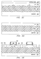
- FIG. 1A shows a variable porosity porous silicon layer which will be used in an SOI substrate
- FIG. 1B shows a variable porosity porous silicon layer to be used in RF isolation.
- FIGS. 2A-E are cross-sections of a partially fabricated integrated circuit structure, showing formation of the disclosed SOI structure, as well as formation of transistors.
- FIGS. 3A-C are cross-sections of a partially fabricated integrated circuit structure, showing formation of the disclosed RF isolation structures.
- FIGS. 4A-B are cross-sections of a partially fabricated integrated circuit structure, showing formation of the disclosed mixed signal isolation structures.
- the layer of porous silicon is formed by anodic oxidation of the top layer of a silicon wafer.
- the electrolyte is generally hydrofluoric acid (HF) with water and a surfactant, e.g., a HF/C2H5OH/H2O solution of approximately 1:2:1.
- HF hydrofluoric acid
- surfactant e.g., a HF/C2H5OH/H2O solution of approximately 1:2:1.
- the formation of pores begins at the exposed surface of the silicon wafer and proceeds isotropically.
- the exposed surface is oxidized with a low current density to create a low porosity surface portion.
- the current density is then increased to give a higher porosity which is optimized for the particular process and provides better isolation.
- the oxidation ends with formation of a high porosity region at the interface to the silicon substrate to provide stress relief between the two layers.
- Provisional patent application No. 60/086,959 filed May 28, 1998, which is hereby incorporated by reference, discloses a layer of porous silicon to be used in the formation of an SOI substrate. That process, which can use the disclosed variable porosity porous silicon, will now be discussed with reference to FIGS. 2A-E, which show a cross-section of the wafer at various points in the disclosed process.
- FIG. 1A is a simplification of FIG. 2A, showing only porous silicon layer 210 and substrate 200 .
- a current density of approximately 1-10 mA/cm2 is used to create a region of low porosity (approximately 15-35 percent) which is approximately 10-50 nm thick.
- the current density is then increased to approximately 10-100 mA/cm2 to create a porosity of about 30-70 percent in region 210 B, which is approximately 5 micron thick.
- region 210 C which is nearest the substrate, a current density of approximately 35-100 mA/cm2 is used to create a region approximately 50-500 nm thick and having a porosity of about 60-80 percent. This high porosity layer provides stress relief between the porous silicon layer and the underlying substrate.
- partial oxidation of the porous silicon is performed, forming regions of SiO2 215 on the surface of the pores 205 .
- a short dip in HF, or a plasma etch, is used to remove the oxide from the top surface of the wafer. Once the surface oxide is removed, the wafer is heated in an atmosphere of H2 at 900-1100 degrees C. for approximately 5-10 minutes to allow the crystalline silicon to reflow and seal the pores on the surface, making the wafer surface once again single crystal silicon.
- Epitaxial layer 220 is then grown on the porous silicon 210 and a capping layer 240 is formed on the epitaxial layer, such as chemical-vapor-deposited (CVD) Si3N4. The capping layer provides structural support to the thin epitaxial layer during the anneal to follow.
- CVD chemical-vapor-deposited
- FIG. 2C shows the layers when this process is partially complete, showing an irregular boundary between the substrate 200 , oxide layer 230 , and epitaxial region 220 .
- the nitride capping layer can either be stripped, or left on to facilitate formation of further isolation structures, such as shallow trench isolation (STI).
- FIG. 2D shows the wafer after stripping of the nitride layer.
- FIG. 2E shows partially fabricated transistors, with trench isolation 260 , gate oxide 270 , gate 280 , sidewall spacers 290 , and implanted regions 292 and 294 , all overlying the buried oxide layer 230 .
- RF radio frequency
- field oxide 108 is grown and transistors 102 are formed, including silicide 110 .
- a resist layer 112 is deposited and patterned to expose the field oxide in those areas in which porous silicon isolation is desired. Exposed portions of field oxide 108 are removed, giving the structure of FIG. 3B, followed by ashing of the resist.
- a hard mask layer 104 e.g. of SiC, is deposited and patterned, by means of a resist layer, to provide opening 118 , which is approximately in the center of the area where the porous silicon is desired. Anodic oxidation is then performed to create region 106 of porous silicon.
- region 106 which overlies substrate 100 has four regions of different porosities.
- a current density of approximately 1-40 mA/cm2 is used to create a region about 50-500 nm thick, having a porosity of approximately 25-50 percent. This low porosity provides desirable material strength in the region of porous silicon.
- the current density is then changed to about 35-100 mA/cm2 to create a porosity of approximately 60-80 percent in region 106 B.
- the thickness of this region will be about 30 percent of the total thickness of the porous silicon region and provides the major part of the isolation.
- a current density of approximately 1-40 mA/cm2 forms region 106 C with a porosity of about 25-50 percent to provide further material strength. This region has a thickness about 20 percent of the total thickness of the layer.
- a current density of about 35-100 mA/cm2 forms final region 106 D, which is about 1 micron thick.
- a porosity of about 60-80 percent provides stress reduction between the porous silicon and the underlying substrate.
- processing of the wafer continues with deposition of the interlevel dielectric and formation of metallization layers.
- Patent application Ser. No. 09/120,215 filed Jul. 21, 1998, which is hereby incorporated by reference, discloses a method for forming lateral porous silicon isolation in high frequency and mixed signal circuits.
- the use of a variable porosity porous silicon in this application will now be discussed with reference to FIGS. 4A-B.
- silicon substrate 1 is overlain by a mask layer 3 , e.g. of silicon carbide, except in windows 2 where the formation of porous silicon is desired. Regions of porous silicon 5 are formed through windows 2 using, e.g., a process such as described above for the RF embodiment.
- a mask layer 3 e.g. of silicon carbide
- digital circuitry 7 and analog circuitry 9 are formed in different regions of the wafer, separated by the porous silicon.
- a dielectric can be formed over the surface of the wafer, with interconnects 13 connecting the digital and analog circuitry, at least some of the interconnects crossing the region of porous silicon.
- TritonX-100 a wetting agent well known in the industry. It appears in preliminary tests that TritonX-100 can be used in much smaller quantities, e.g. 1-3 percent of the total solution. Additionally, the literature on anodic oxidation includes references to numerous organics which are being investigated. Thus, the wetting agents mentioned do not constitute an exhaustive list, but merely a sample of the possibilities.
- the proportions of the materials can be changed to produce porous silicon with the desired characteristics.
- the porosity can also be modified by changing the electrolyte concentrations, with lower HF concentrations yielding higher porosity. It is anticipated, however, that it will be important not to expose the wafer to air, e.g., by pulling the wafer from one electrolyte bath and immersing in another bath during the anodization process. This embodiment is considerably slower than the preferred embodiment, since once the electrolyte were altered, it would be necessary to allow time for the concentration change to wick back into the pores before anodization could be continued.
- the electrolyte concentration can be changed by pumping in more water to reduce HF levels and increase porosity, but a waiting period is necessary to allow the electrolyte concentrations to approach equilibrium within the pores before the current is turned on.
- variable porosity can be created in a porous silicon structure.
- the disclosed process can be used in many other applications which utilize porous silicon.
- variable porosity can be produced in porous silicon layers used in other isolation structures, with appropriate modification of the parameters.
- the isolation for RF applications can be performed prior to the formation of transistors.
Abstract
Varying the porosity through the thickness of a porous silicon layer allows conflicting needs to be met by the same layer: a low porosity surface layer allows a high-quality epitaxial layer of silicon to be grown, or can provide structural support, while greater porosity in other portions of the layer increases circuit isolation and provides stress relief between layers.
Description
This application claim priority under 35 USC §119(e)(1) of provisional application number 60/094,503 filed Jul. 29, 1998.
The present invention relates to integrated circuit structures and fabrication methods, and especially to techniques for creating silicon-on-insulator substrates.
Background: Porous Silicon
Porous silicon is formed by anodic oxidation of a silicon wafer in a solution of hydrofluoric acid and a surfactant, such as ethanol. The size of the pores, the porosity, and the thickness of the porous silicon can be controlled; pore size is typically in the range of 10-20 nm, while porosity is typically in the range of 30-70 percent.
Porous silicon has a low dielectric constant and high resistivity, which make it useful for isolation. Since porous silicon has a high surface area for its volume (a few hundred square meters per cubic centimeter), it can be oxidized much more quickly than bulk silicon.
One prior use of porous silicon is in FIPOS—full isolation by porous oxidized silicon, which uses an epitaxial layer grown on a heavily-doped silicon surface. The heavily-doped layer is selectively converted to porous silicon by anodization through holes in the epitaxial layer, then oxidized to form a buried layer of oxide.
Variable Porosity Porous Silicon
The present application discloses varying the porosity throughout a layer of porous silicon. For example, low porosity is advantageous to provide a good surface for epitaxial silicon growth and to provide material strength, while high porosity layers provide better isolation and a reduction of stresses between the porous silicon and the substrate. Variable porosity allows these different requirements to be met by varied regions within the layer.
Advantages of the disclosed methods include the ability to optimize a layer of porous silicon to meet the opposing requirements.
The disclosed inventions will be described with reference to the accompanying drawings, which show important sample embodiments of the invention and which are incorporated in the specification hereof by reference, wherein:
FIG. 1A shows a variable porosity porous silicon layer which will be used in an SOI substrate, while FIG. 1B shows a variable porosity porous silicon layer to be used in RF isolation.
FIGS. 2A-E are cross-sections of a partially fabricated integrated circuit structure, showing formation of the disclosed SOI structure, as well as formation of transistors.
FIGS. 3A-C are cross-sections of a partially fabricated integrated circuit structure, showing formation of the disclosed RF isolation structures.
FIGS. 4A-B are cross-sections of a partially fabricated integrated circuit structure, showing formation of the disclosed mixed signal isolation structures.
The numerous innovative teachings of the present application will be described with particular reference to the presently preferred embodiment. However, it should be understood that this class of embodiments provides only a few examples of the many advantageous uses of the innovative teachings herein. In general, statements made in the specification of the present application do not necessarily delimit any of the various claimed inventions. Moreover, some statements may apply to some inventive features but not to others.
Overview
In general, the layer of porous silicon is formed by anodic oxidation of the top layer of a silicon wafer. The electrolyte is generally hydrofluoric acid (HF) with water and a surfactant, e.g., a HF/C2H5OH/H2O solution of approximately 1:2:1. The formation of pores begins at the exposed surface of the silicon wafer and proceeds isotropically. Preferably (but not necessarily) the exposed surface is oxidized with a low current density to create a low porosity surface portion. The current density is then increased to give a higher porosity which is optimized for the particular process and provides better isolation. Preferably (but not necessarily) the oxidation ends with formation of a high porosity region at the interface to the silicon substrate to provide stress relief between the two layers.
First Embodiment: Use in SOI
Provisional patent application No. 60/086,959, filed May 28, 1998, which is hereby incorporated by reference, discloses a layer of porous silicon to be used in the formation of an SOI substrate. That process, which can use the disclosed variable porosity porous silicon, will now be discussed with reference to FIGS. 2A-E, which show a cross-section of the wafer at various points in the disclosed process.
A boron-doped silicon substrate 200 is anodically oxidized to form a layer of porous silicon 210, seen in FIG. 2A. FIG. 1A is a simplification of FIG. 2A, showing only porous silicon layer 210 and substrate 200. For the outer layer 210A, where an epitaxial layer is to be grown, a current density of approximately 1-10 mA/cm2 is used to create a region of low porosity (approximately 15-35 percent) which is approximately 10-50 nm thick. The current density is then increased to approximately 10-100 mA/cm2 to create a porosity of about 30-70 percent in region 210B, which is approximately 5 micron thick. For region 210C, which is nearest the substrate, a current density of approximately 35-100 mA/cm2 is used to create a region approximately 50-500 nm thick and having a porosity of about 60-80 percent. This high porosity layer provides stress relief between the porous silicon layer and the underlying substrate.
As seen in FIG. 2B, partial oxidation of the porous silicon is performed, forming regions of SiO2 215 on the surface of the pores 205. A short dip in HF, or a plasma etch, is used to remove the oxide from the top surface of the wafer. Once the surface oxide is removed, the wafer is heated in an atmosphere of H2 at 900-1100 degrees C. for approximately 5-10 minutes to allow the crystalline silicon to reflow and seal the pores on the surface, making the wafer surface once again single crystal silicon. Epitaxial layer 220 is then grown on the porous silicon 210 and a capping layer 240 is formed on the epitaxial layer, such as chemical-vapor-deposited (CVD) Si3N4. The capping layer provides structural support to the thin epitaxial layer during the anneal to follow.
The wafer is then annealed at approximately 1325 degrees C. for approximately six hours. At this temperature, the silicon and silicon dioxide will begin to flow and separate. Over time, the partially-oxidized porous silicon layer separates and coalesces into an oxide layer 230 between slightly thickened epitaxial and substrate layers. FIG. 2C shows the layers when this process is partially complete, showing an irregular boundary between the substrate 200, oxide layer 230, and epitaxial region 220. After the anneal is complete (i.e., interfaces are smooth), the wafer is cooled, then the nitride capping layer can either be stripped, or left on to facilitate formation of further isolation structures, such as shallow trench isolation (STI). FIG. 2D shows the wafer after stripping of the nitride layer. Formation of transistors can then proceed. FIG. 2E shows partially fabricated transistors, with trench isolation 260, gate oxide 270, gate 280, sidewall spacers 290, and implanted regions 292 and 294, all overlying the buried oxide layer 230.
Second Embodiment: Use in RF
Provisional patent application No. 60/069,522, filed Dec. 12, 1997, which is hereby incorporated by reference, discloses a method for forming vertical substrate isolation in radio frequency (RF) circuits by a patterned anodic oxidation of the substrate to selectively form porous silicon in desired areas. A variable porosity porous silicon can be used in this application, which will now be discussed with reference to FIGS. 3A-D.
In this embodiment, as seen in FIG. 3A, field oxide 108 is grown and transistors 102 are formed, including silicide 110.
A resist layer 112 is deposited and patterned to expose the field oxide in those areas in which porous silicon isolation is desired. Exposed portions of field oxide 108 are removed, giving the structure of FIG. 3B, followed by ashing of the resist.
A hard mask layer 104, e.g. of SiC, is deposited and patterned, by means of a resist layer, to provide opening 118, which is approximately in the center of the area where the porous silicon is desired. Anodic oxidation is then performed to create region 106 of porous silicon.
A simplified version of the isolation areas is seen in FIG. 1B, region 106, which overlies substrate 100 has four regions of different porosities. In the uppermost region 106A, a current density of approximately 1-40 mA/cm2 is used to create a region about 50-500 nm thick, having a porosity of approximately 25-50 percent. This low porosity provides desirable material strength in the region of porous silicon.
The current density is then changed to about 35-100 mA/cm2 to create a porosity of approximately 60-80 percent in region 106B. The thickness of this region will be about 30 percent of the total thickness of the porous silicon region and provides the major part of the isolation. Next, a current density of approximately 1-40 mA/cm2 forms region 106C with a porosity of about 25-50 percent to provide further material strength. This region has a thickness about 20 percent of the total thickness of the layer.
Finally, a current density of about 35-100 mA/cm2 forms final region 106D, which is about 1 micron thick. A porosity of about 60-80 percent provides stress reduction between the porous silicon and the underlying substrate.
After formation of the porous silicon regions, processing of the wafer continues with deposition of the interlevel dielectric and formation of metallization layers.
Third Embodiment: Use in Mixed Signal Applications
Patent application Ser. No. 09/120,215, filed Jul. 21, 1998, which is hereby incorporated by reference, discloses a method for forming lateral porous silicon isolation in high frequency and mixed signal circuits. The use of a variable porosity porous silicon in this application will now be discussed with reference to FIGS. 4A-B.
In FIG. 4A, silicon substrate 1 is overlain by a mask layer 3, e.g. of silicon carbide, except in windows 2 where the formation of porous silicon is desired. Regions of porous silicon 5 are formed through windows 2 using, e.g., a process such as described above for the RF embodiment.
After stripping of the SiC layer, digital circuitry 7 and analog circuitry 9 are formed in different regions of the wafer, separated by the porous silicon. A dielectric can be formed over the surface of the wafer, with interconnects 13 connecting the digital and analog circuitry, at least some of the interconnects crossing the region of porous silicon.
Alternate Solutions for Anodic Oxidation
In the anodic oxidation process, other surfactants can be used, such as methanol, isopropanol, and TritonX-100, the latter a wetting agent well known in the industry. It appears in preliminary tests that TritonX-100 can be used in much smaller quantities, e.g. 1-3 percent of the total solution. Additionally, the literature on anodic oxidation includes references to numerous organics which are being investigated. Thus, the wetting agents mentioned do not constitute an exhaustive list, but merely a sample of the possibilities.
In addition to changing the surfactant used, the proportions of the materials can be changed to produce porous silicon with the desired characteristics.
Alternate Embodiment: Varying Electrolyte
In a less preferred embodiment, the porosity can also be modified by changing the electrolyte concentrations, with lower HF concentrations yielding higher porosity. It is anticipated, however, that it will be important not to expose the wafer to air, e.g., by pulling the wafer from one electrolyte bath and immersing in another bath during the anodization process. This embodiment is considerably slower than the preferred embodiment, since once the electrolyte were altered, it would be necessary to allow time for the concentration change to wick back into the pores before anodization could be continued. For example, the electrolyte concentration can be changed by pumping in more water to reduce HF levels and increase porosity, but a waiting period is necessary to allow the electrolyte concentrations to approach equilibrium within the pores before the current is turned on.
Modifications and Variations
As will be recognized by those skilled in the art, the innovative concepts described in the present application can be modified and varied over a tremendous range of applications, and accordingly the scope of patented subject matter is not limited by any of the specific exemplary teachings given, but is only defined by the issued claims.
It should be obvious to one of ordinary skill in the art that the disclosed embodiments are not the only instances in which variable porosity can be created in a porous silicon structure. The disclosed process can be used in many other applications which utilize porous silicon.
In alternate embodiments, the variable porosity can be produced in porous silicon layers used in other isolation structures, with appropriate modification of the parameters.
In a further alternate embodiment, the isolation for RF applications can be performed prior to the formation of transistors.
Claims (13)
1. An integrated circuit structure, comprising:
a substrate defining a planar dimension and comprising:
a non-porous portion;
a region of porous silicon, wherein the porosity of said region varies in a predictable manner and comprising:
a first region along an upper surface removed from said non-porous portion and aligned generally along the planar dimension, wherein the first region has a first porosity;
a second region between the first region and the non-porous portion and aligned generally along the planar dimension, wherein the second region has a second porosity; and
wherein said second porosity is greater than said first porosity.
2. The integrated circuit of claim 1 , further comprising an epitaxial layer on a first surface of said region of porous silicon.
3. The integrated circuit of claim 1 , wherein said region of porous silicon provides lateral isolation for circuit elements.
4. The integrated circuit of claim 1 , wherein said region of porous silicon provides vertical isolation for circuit elements.
5. The integrated circuit of claim 1 :
and further comprising a plurality of circuit elements formed in fixed relationships with respect to said substrate; and
wherein said region of porous silicon provides lateral isolation for the plurality of circuit elements.
6. The integrated circuit of claim 1 :
and further comprising a plurality of circuit elements formed in fixed relationships with respect to said substrate; and
wherein said region of porous silicon provides vertical isolation for the plurality of circuit elements.
7. The integrated circuit of claim 1 :
wherein said first porosity is on an order of about 15-35 percent; and
wherein said second porosity is on an order of about 30-70 percent.
8. The integrated circuit of claim 1 :
wherein said region of porous silicon has a third porosity at locations adjacent said non-porous portion; and
wherein said third porosity is greater than said second porosity.
9. The integrated circuit of claim 8 :
wherein said first porosity is on an order of about 15-35 percent;
wherein said second porosity is on an order of about 30-70 percent; and
wherein said third porosity is on an order of about 60-80 percent.
10. The integrated circuit of claim 8 , further comprising an epitaxial layer on a first surface of said region of porous silicon.
11. The integrated circuit of claim 8 :
wherein said region of porous silicon has a fourth porosity at locations between said locations below said upper surface and said locations adjacent said non-porous portion; and
wherein said third porosity is greater than said fourth porosity.
12. The integrated circuit of claim 11 :
wherein said first porosity is on an order of about 25-50 percent;
wherein said second porosity is on an order of about 60-80 percent;
wherein said third porosity is on an order of about 60-80 percent;
wherein said fourth porosity is on an order of about 25-50 percent.
13. The integrated circuit of claim 11 :
and further comprising a plurality of circuit elements formed in fixed relationships with respect to said substrate; and
wherein said region of porous silicon provides vertical isolation for the plurality of circuit elements.
Priority Applications (1)
| Application Number | Priority Date | Filing Date | Title |
|---|---|---|---|
| US09/346,763 US6376859B1 (en) | 1998-07-29 | 1999-07-01 | Variable porosity porous silicon isolation |
Applications Claiming Priority (2)
| Application Number | Priority Date | Filing Date | Title |
|---|---|---|---|
| US9450398P | 1998-07-29 | 1998-07-29 | |
| US09/346,763 US6376859B1 (en) | 1998-07-29 | 1999-07-01 | Variable porosity porous silicon isolation |
Publications (1)
| Publication Number | Publication Date |
|---|---|
| US6376859B1 true US6376859B1 (en) | 2002-04-23 |
Family
ID=22245546
Family Applications (1)
| Application Number | Title | Priority Date | Filing Date |
|---|---|---|---|
| US09/346,763 Expired - Lifetime US6376859B1 (en) | 1998-07-29 | 1999-07-01 | Variable porosity porous silicon isolation |
Country Status (4)
| Country | Link |
|---|---|
| US (1) | US6376859B1 (en) |
| JP (1) | JP2000156484A (en) |
| KR (1) | KR100591222B1 (en) |
| TW (1) | TW512460B (en) |
Cited By (23)
| Publication number | Priority date | Publication date | Assignee | Title |
|---|---|---|---|---|
| US6489217B1 (en) * | 2001-07-03 | 2002-12-03 | Maxim Integrated Products, Inc. | Method of forming an integrated circuit on a low loss substrate |
| US6541863B1 (en) * | 2000-01-05 | 2003-04-01 | Advanced Micro Devices, Inc. | Semiconductor device having a reduced signal processing time and a method of fabricating the same |
| US6627507B2 (en) * | 1997-12-29 | 2003-09-30 | Texas Instruments Incorporated | Integrated circuit and method of using porous silicon to achieve component isolation in radio frequency applications |
| US6791155B1 (en) | 2002-09-20 | 2004-09-14 | Integrated Device Technology, Inc. | Stress-relieved shallow trench isolation (STI) structure and method for forming the same |
| US20040207083A1 (en) * | 2001-07-18 | 2004-10-21 | Kathrine Giles | Low dielectric constant layers |
| WO2004100256A1 (en) * | 2003-05-07 | 2004-11-18 | Robert Bosch Gmbh | Device comprising a semiconductor circuit |
| FR2857155A1 (en) * | 2003-07-01 | 2005-01-07 | St Microelectronics Sa | Fabrication of a stressed layer of silicon or silicon-germanium alloy on a layer of material with a modifiable mesh parameter, notably for the fabrication of transistors in integrated circuits |
| US20050181572A1 (en) * | 2004-02-13 | 2005-08-18 | Verhoeven Tracy B. | Method for acoustically isolating an acoustic resonator from a substrate |
| WO2006131177A2 (en) * | 2005-06-06 | 2006-12-14 | Universität Stuttgart | Method for producing seed layers for depositing semiconductor material |
| CN1315160C (en) * | 2004-09-30 | 2007-05-09 | 北京大学 | Processing method of SOC silicon substrate |
| US20070176131A1 (en) * | 2005-11-02 | 2007-08-02 | Fujifilm Corporation | Radiation image information detecting panel and radiation image information read-out system |
| EP1959490A1 (en) * | 2007-02-15 | 2008-08-20 | Stmicroelectronics SA | Method of manufacturing a semiconductor-type structure on an insulator |
| CN102064186A (en) * | 2010-11-15 | 2011-05-18 | 王楚雯 | Semiconductor structure and forming method thereof |
| CN102104060A (en) * | 2010-11-15 | 2011-06-22 | 王楚雯 | Semiconductor structure and forming method thereof |
| WO2011156028A2 (en) * | 2010-03-09 | 2011-12-15 | Board Of Regents Of The University Of Texas System | Porous and non-porous nanostructures |
| US20150041822A1 (en) * | 2013-08-06 | 2015-02-12 | Samsung Electronics Co., Ltd. | Semiconductor light emitting device |
| RU2554298C1 (en) * | 2013-12-05 | 2015-06-27 | Федеральное государственное бюджетное учреждение науки Омский научный центр Сибирского отделения Российской академии наук (ОНЦ СО РАН) | Method for manufacturing of multilayer structure of porous silicon-on-insulator |
| US20150286140A1 (en) * | 2012-08-08 | 2015-10-08 | Commissariat A L'energie Atomique Et Aux Energies Alternatives | Substrate for high-resolution electronic lithography and corresponding lithography method |
| TWI560163B (en) * | 2010-08-24 | 2016-12-01 | Corning Inc | Dimensional silica-based porous silicon structures and methods of fabrication |
| US20160359044A1 (en) * | 2015-06-04 | 2016-12-08 | International Business Machines Corporation | FORMATION OF DISLOCATION-FREE SiGe FINFET USING POROUS SILICON |
| US20210020436A1 (en) * | 2019-07-19 | 2021-01-21 | Iqe Plc | Semiconductor material having tunable permittivity and tunable thermal conductivity |
| US11637010B2 (en) * | 2015-07-30 | 2023-04-25 | Taiwan Semiconductor Manufacturing Company, Ltd. | System and method of forming a porous low-k structure |
| EP4220688A3 (en) * | 2022-01-31 | 2023-08-09 | IQE plc | A semiconductor layered structure |
Families Citing this family (5)
| Publication number | Priority date | Publication date | Assignee | Title |
|---|---|---|---|---|
| US7125458B2 (en) * | 2003-09-12 | 2006-10-24 | International Business Machines Corporation | Formation of a silicon germanium-on-insulator structure by oxidation of a buried porous silicon layer |
| US7566482B2 (en) | 2003-09-30 | 2009-07-28 | International Business Machines Corporation | SOI by oxidation of porous silicon |
| US7172930B2 (en) * | 2004-07-02 | 2007-02-06 | International Business Machines Corporation | Strained silicon-on-insulator by anodization of a buried p+ silicon germanium layer |
| EP1897132A4 (en) * | 2005-06-27 | 2014-11-26 | Univ California | Method for fabricating shallow trenches |
| JP5531973B2 (en) * | 2011-01-20 | 2014-06-25 | 信越半導体株式会社 | Bonded substrate and manufacturing method thereof |
Citations (7)
| Publication number | Priority date | Publication date | Assignee | Title |
|---|---|---|---|---|
| US3954523A (en) * | 1975-04-14 | 1976-05-04 | International Business Machines Corporation | Process for fabricating devices having dielectric isolation utilizing anodic treatment and selective oxidation |
| US4180416A (en) * | 1978-09-27 | 1979-12-25 | International Business Machines Corporation | Thermal migration-porous silicon technique for forming deep dielectric isolation |
| US5525374A (en) * | 1992-09-17 | 1996-06-11 | Golden Technologies Company | Method for making ceramic-metal gradient composites |
| US5767561A (en) * | 1997-05-09 | 1998-06-16 | Lucent Technologies Inc. | Integrated circuit device with isolated circuit elements |
| US5767020A (en) | 1991-02-15 | 1998-06-16 | Canon Kabushiki Kaisha | Etching solution for etching porous silicon, etching method using the etching solution and method of preparing semiconductor member using the etching solution |
| US5914183A (en) * | 1993-12-06 | 1999-06-22 | The Secretary Of State For Defence In Her Brittanic Majesty's Government Of The United Kingdom Of Great Britain And Northern Ireland | Porous semiconductor material |
| US6008540A (en) * | 1997-05-28 | 1999-12-28 | Texas Instruments Incorporated | Integrated circuit dielectric and method |
-
1999
- 1999-07-01 US US09/346,763 patent/US6376859B1/en not_active Expired - Lifetime
- 1999-07-28 KR KR1019990030731A patent/KR100591222B1/en not_active IP Right Cessation
- 1999-07-29 JP JP11214770A patent/JP2000156484A/en active Pending
- 1999-08-04 TW TW088112843A patent/TW512460B/en not_active IP Right Cessation
Patent Citations (7)
| Publication number | Priority date | Publication date | Assignee | Title |
|---|---|---|---|---|
| US3954523A (en) * | 1975-04-14 | 1976-05-04 | International Business Machines Corporation | Process for fabricating devices having dielectric isolation utilizing anodic treatment and selective oxidation |
| US4180416A (en) * | 1978-09-27 | 1979-12-25 | International Business Machines Corporation | Thermal migration-porous silicon technique for forming deep dielectric isolation |
| US5767020A (en) | 1991-02-15 | 1998-06-16 | Canon Kabushiki Kaisha | Etching solution for etching porous silicon, etching method using the etching solution and method of preparing semiconductor member using the etching solution |
| US5525374A (en) * | 1992-09-17 | 1996-06-11 | Golden Technologies Company | Method for making ceramic-metal gradient composites |
| US5914183A (en) * | 1993-12-06 | 1999-06-22 | The Secretary Of State For Defence In Her Brittanic Majesty's Government Of The United Kingdom Of Great Britain And Northern Ireland | Porous semiconductor material |
| US5767561A (en) * | 1997-05-09 | 1998-06-16 | Lucent Technologies Inc. | Integrated circuit device with isolated circuit elements |
| US6008540A (en) * | 1997-05-28 | 1999-12-28 | Texas Instruments Incorporated | Integrated circuit dielectric and method |
Non-Patent Citations (5)
| Title |
|---|
| Imai, et al., "Full Isolation Technology by Porous Oxidized Silicon and Its Application to LSIs", 1981 IEEE, IEDM 81-376-IEDM 81-379. |
| Imai, et al., "Full Isolation Technology by Porous Oxidized Silicon and Its Application to LSIs", 1981 IEEE, IEDM 81-376—IEDM 81-379. |
| Patent Abstracts Of Japan; "Semiconductor Basic Material and Production Thereof"; No. 09-162090; pub. date Jun. 20, 1997; S. Nobuhiko, et al. |
| Zorinsky, et al., "The Islands Method-A Manufacturable Porous Silicon SOI Technology", 1986 IEEE, IEDM 86-431-IEDM 86-434. |
| Zorinsky, et al., "The Islands Method—A Manufacturable Porous Silicon SOI Technology", 1986 IEEE, IEDM 86-431—IEDM 86-434. |
Cited By (35)
| Publication number | Priority date | Publication date | Assignee | Title |
|---|---|---|---|---|
| US6627507B2 (en) * | 1997-12-29 | 2003-09-30 | Texas Instruments Incorporated | Integrated circuit and method of using porous silicon to achieve component isolation in radio frequency applications |
| US6541863B1 (en) * | 2000-01-05 | 2003-04-01 | Advanced Micro Devices, Inc. | Semiconductor device having a reduced signal processing time and a method of fabricating the same |
| US6489217B1 (en) * | 2001-07-03 | 2002-12-03 | Maxim Integrated Products, Inc. | Method of forming an integrated circuit on a low loss substrate |
| US20040207083A1 (en) * | 2001-07-18 | 2004-10-21 | Kathrine Giles | Low dielectric constant layers |
| US6963137B2 (en) * | 2001-07-18 | 2005-11-08 | Trikon Holdings Limited | Low dielectric constant layers |
| US6791155B1 (en) | 2002-09-20 | 2004-09-14 | Integrated Device Technology, Inc. | Stress-relieved shallow trench isolation (STI) structure and method for forming the same |
| US7015116B1 (en) | 2002-09-20 | 2006-03-21 | Integrated Device Technology, Inc. | Stress-relieved shallow trench isolation (STI) structure and method for forming the same |
| WO2004100256A1 (en) * | 2003-05-07 | 2004-11-18 | Robert Bosch Gmbh | Device comprising a semiconductor circuit |
| US7279404B2 (en) | 2003-07-01 | 2007-10-09 | Stmicroelectronics S.A. | Process for fabricating strained layers of silicon or of a silicon/germanium alloy |
| FR2857155A1 (en) * | 2003-07-01 | 2005-01-07 | St Microelectronics Sa | Fabrication of a stressed layer of silicon or silicon-germanium alloy on a layer of material with a modifiable mesh parameter, notably for the fabrication of transistors in integrated circuits |
| US20050037599A1 (en) * | 2003-07-01 | 2005-02-17 | Stmicroelectronics S.A. | Process for fabricating strained layers of silicon or of a silicon/germanium alloy |
| US20050181572A1 (en) * | 2004-02-13 | 2005-08-18 | Verhoeven Tracy B. | Method for acoustically isolating an acoustic resonator from a substrate |
| CN1315160C (en) * | 2004-09-30 | 2007-05-09 | 北京大学 | Processing method of SOC silicon substrate |
| WO2006131177A3 (en) * | 2005-06-06 | 2007-03-08 | Univ Stuttgart | Method for producing seed layers for depositing semiconductor material |
| WO2006131177A2 (en) * | 2005-06-06 | 2006-12-14 | Universität Stuttgart | Method for producing seed layers for depositing semiconductor material |
| US20070176131A1 (en) * | 2005-11-02 | 2007-08-02 | Fujifilm Corporation | Radiation image information detecting panel and radiation image information read-out system |
| EP1959490A1 (en) * | 2007-02-15 | 2008-08-20 | Stmicroelectronics SA | Method of manufacturing a semiconductor-type structure on an insulator |
| US8178426B2 (en) * | 2007-02-15 | 2012-05-15 | Stmicroelectronics S.A. | Method for manufacturing a structure of semiconductor-on-insulator type |
| US20080197447A1 (en) * | 2007-02-15 | 2008-08-21 | Stmicroelectronics S.A. | Method for manufacturing a structure of semiconductor-on-insulator type |
| WO2011156028A2 (en) * | 2010-03-09 | 2011-12-15 | Board Of Regents Of The University Of Texas System | Porous and non-porous nanostructures |
| WO2011156028A3 (en) * | 2010-03-09 | 2014-03-20 | Board Of Regents Of The University Of Texas System | Porous and non-porous nanostructures |
| TWI560163B (en) * | 2010-08-24 | 2016-12-01 | Corning Inc | Dimensional silica-based porous silicon structures and methods of fabrication |
| CN102064186A (en) * | 2010-11-15 | 2011-05-18 | 王楚雯 | Semiconductor structure and forming method thereof |
| CN102104060A (en) * | 2010-11-15 | 2011-06-22 | 王楚雯 | Semiconductor structure and forming method thereof |
| CN102104060B (en) * | 2010-11-15 | 2013-03-20 | 王楚雯 | Semiconductor structure and forming method thereof |
| US20150286140A1 (en) * | 2012-08-08 | 2015-10-08 | Commissariat A L'energie Atomique Et Aux Energies Alternatives | Substrate for high-resolution electronic lithography and corresponding lithography method |
| US9543470B2 (en) * | 2013-08-06 | 2017-01-10 | Samsung Electronics Co., Ltd. | Semiconductor light emitting device |
| US20150041822A1 (en) * | 2013-08-06 | 2015-02-12 | Samsung Electronics Co., Ltd. | Semiconductor light emitting device |
| RU2554298C1 (en) * | 2013-12-05 | 2015-06-27 | Федеральное государственное бюджетное учреждение науки Омский научный центр Сибирского отделения Российской академии наук (ОНЦ СО РАН) | Method for manufacturing of multilayer structure of porous silicon-on-insulator |
| US20160359044A1 (en) * | 2015-06-04 | 2016-12-08 | International Business Machines Corporation | FORMATION OF DISLOCATION-FREE SiGe FINFET USING POROUS SILICON |
| US10833175B2 (en) * | 2015-06-04 | 2020-11-10 | International Business Machines Corporation | Formation of dislocation-free SiGe finFET using porous silicon |
| US11637010B2 (en) * | 2015-07-30 | 2023-04-25 | Taiwan Semiconductor Manufacturing Company, Ltd. | System and method of forming a porous low-k structure |
| US20210020436A1 (en) * | 2019-07-19 | 2021-01-21 | Iqe Plc | Semiconductor material having tunable permittivity and tunable thermal conductivity |
| US11355340B2 (en) * | 2019-07-19 | 2022-06-07 | Iqe Plc | Semiconductor material having tunable permittivity and tunable thermal conductivity |
| EP4220688A3 (en) * | 2022-01-31 | 2023-08-09 | IQE plc | A semiconductor layered structure |
Also Published As
| Publication number | Publication date |
|---|---|
| KR100591222B1 (en) | 2006-06-19 |
| TW512460B (en) | 2002-12-01 |
| KR20000012018A (en) | 2000-02-25 |
| JP2000156484A (en) | 2000-06-06 |
Similar Documents
| Publication | Publication Date | Title |
|---|---|---|
| US6376859B1 (en) | Variable porosity porous silicon isolation | |
| US6376285B1 (en) | Annealed porous silicon with epitaxial layer for SOI | |
| JPH1174460A (en) | Manufacture of device | |
| US4016017A (en) | Integrated circuit isolation structure and method for producing the isolation structure | |
| KR100265539B1 (en) | Substrate and production method thereof | |
| US6653209B1 (en) | Method of producing silicon thin film, method of constructing SOI substrate and semiconductor device | |
| US6806171B1 (en) | Method of producing a thin layer of crystalline material | |
| KR100235398B1 (en) | Method for production of soi substrate by pasting and soi substrate | |
| KR100246902B1 (en) | Semiconductor substrate and fabrication method for the same | |
| KR100260832B1 (en) | Semiconductor substrate and manufacture thereof | |
| JPH05275663A (en) | Semiconductor element substrate and manufacture thereof | |
| US5512509A (en) | Method for forming an isolation layer in a semiconductor device | |
| US20060289962A1 (en) | An isolation region for use in a semiconductor device | |
| TW200406893A (en) | Substrate and manufacturing method therefor | |
| US4876216A (en) | Semiconductor integrated circuit manufacturing process providing oxide-filled trench isolation of circuit devices | |
| EP0938132A3 (en) | Porous region removing method and semiconductor substrate manufacturing method | |
| US5296086A (en) | Method for manufacturing semiconductor device having grown layer on insulating layer | |
| US6187649B1 (en) | Shallow trench isolation process | |
| JP3297600B2 (en) | Manufacturing method of semiconductor substrate | |
| JPH05102292A (en) | Manufacture of isoplanar-separating type active region | |
| US5402989A (en) | Method for manufacturing semiconductor device having grown layer on insulating layer | |
| JP2004103600A (en) | Substrate and its manufacturing method | |
| US9356094B2 (en) | Method for making a semi-conducting substrate located on an insulation layer | |
| US20020173119A1 (en) | Method for manufacturing a silicon wafer | |
| US6217647B1 (en) | Method for producing a monocrystalline layer of a conducting or semiconducting material |
Legal Events
| Date | Code | Title | Description |
|---|---|---|---|
| AS | Assignment |
Owner name: TEXAS INSTRUMENTS INCORPORATED, TEXAS Free format text: ASSIGNMENT OF ASSIGNORS INTEREST;ASSIGNORS:SWANSON, LELAND S.;JOYNER, KEITH A.;REEL/FRAME:010087/0994;SIGNING DATES FROM 19980805 TO 19980810 |
|
| STCF | Information on status: patent grant |
Free format text: PATENTED CASE |
|
| FPAY | Fee payment |
Year of fee payment: 4 |
|
| FPAY | Fee payment |
Year of fee payment: 8 |
|
| FPAY | Fee payment |
Year of fee payment: 12 |