US6380628B2 - Microstructure liner having improved adhesion - Google Patents
Microstructure liner having improved adhesion Download PDFInfo
- Publication number
- US6380628B2 US6380628B2 US09/377,329 US37732999A US6380628B2 US 6380628 B2 US6380628 B2 US 6380628B2 US 37732999 A US37732999 A US 37732999A US 6380628 B2 US6380628 B2 US 6380628B2
- Authority
- US
- United States
- Prior art keywords
- liner
- substrate
- damascene structure
- roughened
- sidewall
- Prior art date
- Legal status (The legal status is an assumption and is not a legal conclusion. Google has not performed a legal analysis and makes no representation as to the accuracy of the status listed.)
- Expired - Fee Related
Links
Images


Classifications
-
- H—ELECTRICITY
- H01—ELECTRIC ELEMENTS
- H01L—SEMICONDUCTOR DEVICES NOT COVERED BY CLASS H10
- H01L21/00—Processes or apparatus adapted for the manufacture or treatment of semiconductor or solid state devices or of parts thereof
- H01L21/70—Manufacture or treatment of devices consisting of a plurality of solid state components formed in or on a common substrate or of parts thereof; Manufacture of integrated circuit devices or of parts thereof
- H01L21/71—Manufacture of specific parts of devices defined in group H01L21/70
- H01L21/768—Applying interconnections to be used for carrying current between separate components within a device comprising conductors and dielectrics
- H01L21/76838—Applying interconnections to be used for carrying current between separate components within a device comprising conductors and dielectrics characterised by the formation and the after-treatment of the conductors
- H01L21/76841—Barrier, adhesion or liner layers
- H01L21/76853—Barrier, adhesion or liner layers characterized by particular after-treatment steps
- H01L21/76861—Post-treatment or after-treatment not introducing additional chemical elements into the layer
- H01L21/76862—Bombardment with particles, e.g. treatment in noble gas plasmas; UV irradiation
-
- H—ELECTRICITY
- H01—ELECTRIC ELEMENTS
- H01L—SEMICONDUCTOR DEVICES NOT COVERED BY CLASS H10
- H01L21/00—Processes or apparatus adapted for the manufacture or treatment of semiconductor or solid state devices or of parts thereof
- H01L21/70—Manufacture or treatment of devices consisting of a plurality of solid state components formed in or on a common substrate or of parts thereof; Manufacture of integrated circuit devices or of parts thereof
- H01L21/71—Manufacture of specific parts of devices defined in group H01L21/70
- H01L21/768—Applying interconnections to be used for carrying current between separate components within a device comprising conductors and dielectrics
- H01L21/76801—Applying interconnections to be used for carrying current between separate components within a device comprising conductors and dielectrics characterised by the formation and the after-treatment of the dielectrics, e.g. smoothing
- H01L21/76802—Applying interconnections to be used for carrying current between separate components within a device comprising conductors and dielectrics characterised by the formation and the after-treatment of the dielectrics, e.g. smoothing by forming openings in dielectrics
- H01L21/76816—Aspects relating to the layout of the pattern or to the size of vias or trenches
-
- H—ELECTRICITY
- H01—ELECTRIC ELEMENTS
- H01L—SEMICONDUCTOR DEVICES NOT COVERED BY CLASS H10
- H01L21/00—Processes or apparatus adapted for the manufacture or treatment of semiconductor or solid state devices or of parts thereof
- H01L21/70—Manufacture or treatment of devices consisting of a plurality of solid state components formed in or on a common substrate or of parts thereof; Manufacture of integrated circuit devices or of parts thereof
- H01L21/71—Manufacture of specific parts of devices defined in group H01L21/70
- H01L21/768—Applying interconnections to be used for carrying current between separate components within a device comprising conductors and dielectrics
- H01L21/76838—Applying interconnections to be used for carrying current between separate components within a device comprising conductors and dielectrics characterised by the formation and the after-treatment of the conductors
- H01L21/76841—Barrier, adhesion or liner layers
- H01L21/76843—Barrier, adhesion or liner layers formed in openings in a dielectric
-
- H—ELECTRICITY
- H01—ELECTRIC ELEMENTS
- H01L—SEMICONDUCTOR DEVICES NOT COVERED BY CLASS H10
- H01L21/00—Processes or apparatus adapted for the manufacture or treatment of semiconductor or solid state devices or of parts thereof
- H01L21/70—Manufacture or treatment of devices consisting of a plurality of solid state components formed in or on a common substrate or of parts thereof; Manufacture of integrated circuit devices or of parts thereof
- H01L21/71—Manufacture of specific parts of devices defined in group H01L21/70
- H01L21/768—Applying interconnections to be used for carrying current between separate components within a device comprising conductors and dielectrics
- H01L21/76838—Applying interconnections to be used for carrying current between separate components within a device comprising conductors and dielectrics characterised by the formation and the after-treatment of the conductors
- H01L21/76841—Barrier, adhesion or liner layers
- H01L21/76853—Barrier, adhesion or liner layers characterized by particular after-treatment steps
- H01L21/76865—Selective removal of parts of the layer
-
- H—ELECTRICITY
- H01—ELECTRIC ELEMENTS
- H01L—SEMICONDUCTOR DEVICES NOT COVERED BY CLASS H10
- H01L21/00—Processes or apparatus adapted for the manufacture or treatment of semiconductor or solid state devices or of parts thereof
- H01L21/70—Manufacture or treatment of devices consisting of a plurality of solid state components formed in or on a common substrate or of parts thereof; Manufacture of integrated circuit devices or of parts thereof
- H01L21/71—Manufacture of specific parts of devices defined in group H01L21/70
- H01L21/768—Applying interconnections to be used for carrying current between separate components within a device comprising conductors and dielectrics
- H01L21/76838—Applying interconnections to be used for carrying current between separate components within a device comprising conductors and dielectrics characterised by the formation and the after-treatment of the conductors
- H01L21/76841—Barrier, adhesion or liner layers
- H01L21/76871—Layers specifically deposited to enhance or enable the nucleation of further layers, i.e. seed layers
Definitions
- the present invention relates generally to integrated circuits and, more specifically, to prevention of interlaminar de-lamination in chip wiring and packaging structures.
- Copper is frequently used in chip wiring and packaging structures. Often, to prevent copper from contaminating the silicon or the dielectric in the device, a barrier layer is interposed between the silicon and the copper or between the dielectric and the copper. To maintain the structural integrity of the wiring structure, however, the adhesion between the barrier and dielectric and the barrier and the copper must be sufficient to survive subsequent processing.
- FIGS. 1 and 2 there are shown typical via and line structures of the prior art illustrating the critical parameters affecting adhesion.
- a suitable photoresist material (not shown) on a substrate 12 , typically an insulator or dielectric such as an oxide, and then imaging the photoresist in a desired pattern of vias and lines.
- the photoresist image is then transferred onto substrate 12 by reactive ion etching (RIE) methods well known in the art.
- RIE reactive ion etching
- Via 10 and line 20 are then typically coated by a suitable barrier layer 14 , after which the structure is filled with a suitable metal 30 , such as copper, by electrodeposition, sputtering, or chemical vapor deposition (CVD) processes and the like, also well known in the art.
- a suitable metal 30 such as copper, by electrodeposition, sputtering, or chemical vapor deposition (CVD) processes and the like, also well known in the art.
- Excess metal overburden (not shown) that may protrude above the surface 11 of substrate 12 , after the deposition step, may then be planarized to produce the finished structures as shown
- a cylindrical conductive via 10 in substrate 12 typically has a diameter d and a height h.
- Circular bottom 16 has an area A b and cylindrical wall 18 has a circumferential area A c .
- a b 1 4 ⁇ ⁇ ⁇ ⁇ d 2 ( 1 )
- a c ⁇ ⁇ ⁇ d ⁇ ⁇ h ( 2 )
- a c A b 4 ⁇ h d ( 3 )
- the ratio A c /A b is equal to 4.
- the ratio A c /A b thus increases linearly with an increase in aspect ratio.
- line 20 has a width W a depth D and a length L.
- the corresponding line floor 22 has an area A f and the total sidewall area A w comprises the sum of the areas of the four walls 23 and 24 as follows:
- Equation 6 reduces to: A w A f ⁇ 2 ⁇ D W ( 7 )
- FIG. 2 depicts the balance of stresses related to adhesion in via 10 .
- tensile stress ⁇ L is opposed by adhesion stress ⁇ L such that:
- the adhesion stress ⁇ V exceeds the adhesion strength of any of the bonds between conductive via 10 , barrier layer 14 , and substrate 12 .
- de-lamination may occur if ⁇ L exceeds the corresponding adhesion strength of any of the bonds between line 20 , barrier layer 14 , and substrate 12 .
- the adhesion strength of certain desired via and line materials, such as copper, to certain desired barrier layers or dielectrics may be relatively low. As the size of vias and lines are reduced, the surface area of the bonding surfaces also becomes reduced, whereas the adhesion strength and tensile stresses may be. the same. Hence, finer wiring structures may be exposed to increased interlaminar de-lamination or local separation of the dielectric or barrier layer from the metal structure of the vias or lines.
- the present invention provides a damascene structure extending into an insulating substrate, the structure having a sidewall and a bottom, a liner on the sidewall and the bottom, and a conductive fill on the liner.
- the improvement comprises the liner having a roughened surface in contact with the conductive fill.
- the roughened liner surface may comprise a serrated pattern along a longitudinal section parallel to the substrate surface, and may further comprise a serrated pattern along a cross section intersecting the substrate surface.
- the damascene structure sidewall may also have a roughened surface in contact with the liner, in particular a roughened surface that comprises a serrated pattern along a longitudinal section parallel to the substrate surface.
- the liner may have a smooth surface over the damascene structure bottom, which may be smooth itself.
- the invention also comprises a process for fabricating a conductive damascene structure in a substrate.
- the process comprises applying a photoresist over the top surface of a substrate and exposing the photoresist using exposure conditions that create a standing wave in the resist during resist exposure.
- a damascene structure pattern is revealed having a plurality of serrations extending in a longitudinal plane substantially parallel to the substrate top surface.
- the pattern is transferred to the substrate to create in the pattern a damascene structure having a bottom and serrated sidewall with a plurality of serrations along a longitudinal section substantially parallel to the substrate top surface.
- a liner is applied over the bottom and over the sidewall in the substrate.
- the damascene structure is then filled with a conductive fill over the liner.
- the liner may be applied over the sidewall in the substrate such that the liner surface has a plurality of serrations along a longitudinal section parallel to the substrate top surface.
- the liner may further be applied over the sidewall in the substrate such that the liner surface has a plurality of serrations along a cross-sectional plane intersecting the substrate top surface.
- the roughened surface may be achieved by applying a partial layer of liner material over the substrate, removing a portion of the partial layer, and repeating the application and removal steps until the liner sidewall conforms to the serrated sidewall in the substrate and has a sufficiently roughened surface.
- the step of applying the conductive fill may further comprise applying a seed layer over the liner and then applying the conductive fill over the seed layer, the seed layer and the conductive fill comprising similar conductive materials.
- the step of applying the seed layer may comprise applying a partial seed layer of the conductive material over the liner, removing a portion of the partial seed layer, and repeating the application and removal steps until the seed layer is sufficiently deposited in conformance to the liner.
- the invention also comprises a method for enhancing adhesion between one or more layers of a damascene structure in a substrate.
- the method comprises creating the damascene structure with a roughened sidewall in the substrate.
- the damascene structure may further have a smooth bottom and, optionally, a liner over the roughened sidewall and smooth bottom, the liner having a roughened surface over the sidewall and smooth surface over the bottom.
- the method may further comprise disposing conductive material over the liner.
- the conductive fill may be applied by first applying a seed layer over the liner, the seed layer comprising a thin layer of the conductive material, and then depositing a remainder of the conductive material over the seed layer.
- FIG. 1 is a perspective view of a typical via and line in a substrate as are known in the prior art
- FIG. 2 is a cross-sectional view of the via and line taken along the line 2 — 2 of FIG. 1;
- FIG. 3 is a perspective, partial cross-sectional view of an exemplary via and line according to the present invention.
- FIGS. 4A through 4F are cross-sectional and perspective, partial cross-sectional illustrations of an exemplary process for manufacture of an exemplary via and line of the present invention with FIG. 4A showing a cross-section of a substrate undergoing a photoresist exposure step;
- FIG. 4B shows a perspective, partial cross-section of the substrate of FIG. 4A after photoresist development
- FIG. 4C shows a cross-section of the substrate of FIG. 4B after an etching step
- FIG. 4D shows a cross-section of the substrate of FIG. 4C after deposition of the liner
- FIG. 4E shows a cross-section of the substrate of FIG. 4D after deposition of a seed layer
- FIG. 4F shows a cross-section of the substrate of FIG. 4E after deposition of conductive fill and before a planarization step.
- a damascene process is a process used in some aspects of semiconductor fabrication. It is a process of inlaying a metal into a predefined pattern, typically in a dielectric layer. The process is typically performed by defining the desired pattern into a dielectric film; depositing metal over the entire surface by either physical vapor deposition, chemical vapor deposition, or evaporation; then polishing back the top surface in such a way that the top surface is planarized and the metal pattern is only located in the predefined regions of the dielectric layer.
- the damascene process has been used in manufacturing of metal wiring lines, including the bit-lines for a dynamic random access memory (DRAM) capacitor.
- DRAM dynamic random access memory
- Damascene technology is a common method of fabricating interconnects.
- damascene refers to the steps of patterning an insulator to form recesses, filling the recesses with a metal, and then removing the excess metal above the recesses. This process can be repeated as needed to form the desired number of stacked interconnects.
- these damascene structures are laid out in pairs, a process referred to as dual damascene.
- the present invention constitutes an improved damascene structure and an improved process for making such a structure. The improvements are best explained using the equations outlined above.
- FIG. 3 there is shown a partial cross section, partial perspective view of a via 10 ′ and a line 20 ′ of the present invention in which sidewalls 18 ′ and 24 ′ are roughened.
- sidewalls 18 ′ and 24 ′ each comprise a pattern of serrations having coplanar peaks 50 and valleys 52 along planar surface 11 .
- This serrated pattern also extends into substrate 12 such that any longitudinal section (such as along plane I) of via 10 ′ or line 20 ′ parallel to surface 11 also has the same, regular serrated pattern of peaks 50 and valleys 52 .
- a “regular” serrated pattern is meant that a comparison of any two longitudinal section planes reveals peaks 50 and valleys 52 aligned with one another from plane to plane.
- Liner 14 ′ in via 10 ′ and line 20 ′ also has roughened sidewalls 15 and 25 , respectively.
- the roughness in liner 14 ′ may comprise not only serrations extending along longitudinal section planes parallel to the plane of surface 11 (in conformance with serrated sidewalls 18 ′ and 24 ′), but also serrations extending along cross-sectional planes such as cross-sectional plane II shown in FIG. 3 .
- the serrations of liner 14 ′ along cross-sectional planes are typically not in a regular pattern (i.e., a comparison of two cross-sectional planes typically does not reveal aligned peaks 50 and valleys 52 ).
- liner 14 ′ is roughened along both longitudinal section and cross section planes, a comparison, the pattern in both planes is typically irregular, as the irregularity in the cross-sectional plane disrupts any regularity in the longitudinal section plane.
- the serrations in liner 14 ′ may also comprise a regular pattern of peaks 50 and valleys 52 in some cases, however, particularly when the liner serrations merely conform to serrations in sidewall 15 or 25 without serrations in the cross-sectional planes.
- the roughened liner sidewalls by virtue of their wavy shape, create greater surface area.
- the effective length L R , height h R , and depth DR of liner 14 ′ as shown in FIG. 3 may be two-to-three times greater than the effective length, height, and depth of corresponding smooth-walled liners over smooth sidewalls.
- Such increases in h R and D R linearly increase corresponding ratios A c /A b and A w /A f , assuming a constant d and W, and thus proportionately decrease ⁇ v and ⁇ L .
- the selectively increased surface roughness of liner roughened sidewalls 15 and 25 not only increases surface area, but also creates micro-interlocking structures on the sidewalls.
- Bottom 16 and floor 22 may be left unroughened, creating a “dual microstructure liner.”
- the “dual microstructure” refers to the roughened microstructure on the vertical roughened sidewalls 15 and 25 of liner 14 ′ of via 10 ′ and line 20 ′, respectively, as compared to the smooth microstructure on bottom 16 and floor 22 of liner 14 ′, respectively.
- Via 10 ′ and line 20 ′ may be filled with conductive fill or metal 30 , such as copper, as shown in FIG. 3 .
- photoresist 40 is deposited on substrate 12 as shown in FIG. 4 A.
- Photoresist 40 and substrate 12 comprise any of the standard materials well known in the art.
- An illumination source (not shown) shines illumination 41 through a patterned mask 42 under exposure conditions chosen to create a standing wave in photoresist 40 during resist exposure.
- standing waves are produced as a result of interference wave reflections from the resist-substrate interface, and are present at: 2 ⁇ N ⁇ ⁇ ⁇ 2 ⁇ n ( 15 )
- n index of refraction of photoresist 40
- N an integer.
- photoresist 40 (having a known index of refraction) and the wavelength of the exposure source can be optimized to provide a standing wave during exposure, whereas normally standing waves are avoided to provide maximum line resolution.
- the standing wave creates a serrated pattern in photoresist 40 having a reticulated or wavy edge 43 , shown in FIG. 4B after development of photoresist 40 , unlike straight sidewalls 18 and 24 as shown in FIG. 1 created by typical exposure conditions.
- the serrated pattern is then transferred into substrate 12 by RIE, creating via 10 ′ and line 20 ′ as shown in FIG. 4 C.
- sidewalls 18 ′ and 24 ′ are serrated along the plane of surface 11 of substrate 12 , the cross-sectional profile of the sidewalls along the depth of via 10 ′ and line 20 ′ as etched by traditional RIE processes is still straight.
- Barrier layer or liner 14 ′ is then deposited in via 10 ′ and line 20 ′ as shown in FIG. 4 D.
- a liner 14 ′ of tantalum, titanium, or tungsten may be deposited by chemical vapor deposition (CVD) for use with copper lines.
- CVD chemical vapor deposition
- liner 14 ′ may be deposited by using multiple deposition and sputtering processes. Such a multiple deposition process not only conforms liner 14 ′ to the serrations of the sidewall along a longitudinal section, but may also provide serrations in the cross-sectional plane perpendicular to the top surface of substrate 12 , as shown in FIG. 4 D.
- an initial thin layer 14 a of liner material is deposited, for instance having a thickness of 300 Angstroms, after which about 40% to about 80% of the deposited initial thin layer 14 a is sputtered off.
- This deposition and sputtering process is repeated typically more than once.
- liner 14 ′ may comprise four thin layers 14 a , 14 b , 14 c , and 14 d , as shown in FIG. 4D for example, having roughened sidewalls 15 and 25 .
- Globular deposition conditions as are known in the art, such as a PVD sputtering technique, may be chosen in the deposition steps to further enhance the roughness of deposited liner 14 ′.
- a single deposition process may be used if it is only desired to conform liner 14 ′ to the serrations of the sidewall without adding additional roughness in the cross-sectional profile.
- a similar deposition and sputtering process may be used to deposit a seed layer 19 of conductive material, as shown in FIG. 4E, before filling via 10 ′ and 20 ′ with conductive fill or metal 30 as shown in FIG. 4 F.
- Seed layer 19 typically comprises the same conductive material as fill or metal 30 , such as copper, and is used to improve adherence of the conductive fill or metal 30 to liner 14 ′ on sidewalls 15 and 25 .
- Conductive fill or metal 30 may be applied by electroplating in a suitable Cu plating bath, for example, or may be applied by CVD or PVD methods or combinations of such methods, as are known in the art.
- any metal overburden 44 is typically planarized by a chemical mechanical polishing (CMP) process or any process known in the art, to produce the completed via 10 ′ and line 20 ′ as shown in FIG. 3 .
- CMP chemical mechanical polishing
- the micro-interlocking sidewall structure created by the present invention enhances the structural integrity of the metal-substrate interface by increasing surface area for improved adhesion.
- the roughened sidewall not only provides better chemical adhesion, but also mechanically anchors the conductive metal to the sidewall. Furthermore, the roughened sidewalls also provide resistance to electron migration.
- the smooth bottom structure is preferred for minimized contact resistance and current crowding at the via-line interface.
- the dual microstructure liner provides excellent de-lamination resistance while in turn enhancing electro-migration properties.
- the properties of and process for making the damascene structure of the present invention are particularly useful for copper vias and lines, such a structure and process are equally applicable to other conductive fills as well, including, for example, aluminum.
Abstract
A damascene structure, such as a conductive line or via, having a liner with a roughened surface between the substrate and the conductive fill and, preferably, a smooth bottom. The substrate underneath the liner may also have a roughened sidewall and smooth bottom. Such a structure provides enhanced adhesion between one or more layers of the damascene structure. The damascene structure may be manufactured by applying a photoresist over a substrate top surface, exposing the photoresist under conditions that create a standing wave in the resist, and developing the photoresist to provide a pattern having the desired roughened or serrated outline. The pattern is transferred into the substrate, the liner is applied over the substrate bottom and sidewalls, and the liner is filled with conductive material. A roughened liner surface may be achieved by applying a partial layer of liner material over the substrate, removing a portion of the partial layer, and repeating the application and removal steps.
Description
The present invention relates generally to integrated circuits and, more specifically, to prevention of interlaminar de-lamination in chip wiring and packaging structures.
Copper (Cu) is frequently used in chip wiring and packaging structures. Often, to prevent copper from contaminating the silicon or the dielectric in the device, a barrier layer is interposed between the silicon and the copper or between the dielectric and the copper. To maintain the structural integrity of the wiring structure, however, the adhesion between the barrier and dielectric and the barrier and the copper must be sufficient to survive subsequent processing.
Copper adheres poorly to most dielectrics and to some otherwise highly-desirable barrier films. As chip wiring ground rules continue to shrink, adhesion becomes an increasingly critical issue in chip fabrication, because the critical length for adequate adhesion and stress transfer within the wiring structure does not decrease monotonously with the dimensions of the lines and vias. For example, referring now to FIGS. 1 and 2, there are shown typical via and line structures of the prior art illustrating the critical parameters affecting adhesion.
Traditional fabrication processes for damascene structures, such as via 10 or line 20, comprise first depositing a suitable photoresist material (not shown) on a substrate 12, typically an insulator or dielectric such as an oxide, and then imaging the photoresist in a desired pattern of vias and lines. The photoresist image is then transferred onto substrate 12 by reactive ion etching (RIE) methods well known in the art. Via 10 and line 20 are then typically coated by a suitable barrier layer 14, after which the structure is filled with a suitable metal 30, such as copper, by electrodeposition, sputtering, or chemical vapor deposition (CVD) processes and the like, also well known in the art. Excess metal overburden (not shown) that may protrude above the surface 11 of substrate 12, after the deposition step, may then be planarized to produce the finished structures as shown in FIGS. 1 and 2.
As shown in FIGS. 1 and 2, a cylindrical conductive via 10 in substrate 12 typically has a diameter d and a height h. Circular bottom 16 has an area Ab and cylindrical wall 18 has a circumferential area Ac. Thus, the surface areas of the interfaces between via 10, barrier layer 14, and substrate 12 can be expressed as follows: 
When height h and diameter d are equal, i.e., when via 10 has an aspect ratio h/d equal to 1, the ratio Ac/Ab is equal to 4. The ratio Ac/Ab thus increases linearly with an increase in aspect ratio.
Also shown in FIGS. 1 and 2, line 20 has a width W a depth D and a length L. The corresponding line floor 22 has an area Af and the total sidewall area Aw comprises the sum of the areas of the four walls 23 and 24 as follows:
The corresponding ratio of line wall to floor area is thus: 
Because L is much greater than both Wand D, Equation 6 reduces to: 
Thus, for a line aspect ratio D/W equal to 1, Aw/Af equals 2. As the line aspect ratio increases, Aw/Af increases linearly.
FIG. 2 depicts the balance of stresses related to adhesion in via 10. Tensile stress σv in force per unit area acting on conductive via 10 is opposed by adhesion stress τv in force per unit area such that: 
Equation 8 reduces to: 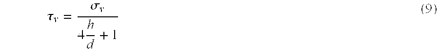
Thus, for an aspect ratio of 1, τV=σV/5.
Similarly, with respect to line 20, tensile stress σL is opposed by adhesion stress τL such that:

Again, because L>>D and L>>W, the following approximation may be used: 
Thus, where the line aspect ratio equals 1 (i.e., W=D), then τL=σL/3.
If the adhesion stress τV exceeds the adhesion strength of any of the bonds between conductive via 10, barrier layer 14, and substrate 12, de-lamination may ensue. Similarly, de-lamination may occur if τL exceeds the corresponding adhesion strength of any of the bonds between line 20, barrier layer 14, and substrate 12. As described earlier, the adhesion strength of certain desired via and line materials, such as copper, to certain desired barrier layers or dielectrics may be relatively low. As the size of vias and lines are reduced, the surface area of the bonding surfaces also becomes reduced, whereas the adhesion strength and tensile stresses may be. the same. Hence, finer wiring structures may be exposed to increased interlaminar de-lamination or local separation of the dielectric or barrier layer from the metal structure of the vias or lines.
Thus, there is a need in the art for methods, structures, and processes of creating such structures to prevent interlaminar de-lamination.
To meet this and other needs, and in view of its purposes, the present invention provides a damascene structure extending into an insulating substrate, the structure having a sidewall and a bottom, a liner on the sidewall and the bottom, and a conductive fill on the liner. The improvement comprises the liner having a roughened surface in contact with the conductive fill. The roughened liner surface may comprise a serrated pattern along a longitudinal section parallel to the substrate surface, and may further comprise a serrated pattern along a cross section intersecting the substrate surface. The damascene structure sidewall may also have a roughened surface in contact with the liner, in particular a roughened surface that comprises a serrated pattern along a longitudinal section parallel to the substrate surface. The liner may have a smooth surface over the damascene structure bottom, which may be smooth itself.
The invention also comprises a process for fabricating a conductive damascene structure in a substrate. The process comprises applying a photoresist over the top surface of a substrate and exposing the photoresist using exposure conditions that create a standing wave in the resist during resist exposure. Upon developing the photoresist, a damascene structure pattern is revealed having a plurality of serrations extending in a longitudinal plane substantially parallel to the substrate top surface. The pattern is transferred to the substrate to create in the pattern a damascene structure having a bottom and serrated sidewall with a plurality of serrations along a longitudinal section substantially parallel to the substrate top surface. A liner is applied over the bottom and over the sidewall in the substrate. The damascene structure is then filled with a conductive fill over the liner.
The liner may be applied over the sidewall in the substrate such that the liner surface has a plurality of serrations along a longitudinal section parallel to the substrate top surface. The liner may further be applied over the sidewall in the substrate such that the liner surface has a plurality of serrations along a cross-sectional plane intersecting the substrate top surface. The roughened surface may be achieved by applying a partial layer of liner material over the substrate, removing a portion of the partial layer, and repeating the application and removal steps until the liner sidewall conforms to the serrated sidewall in the substrate and has a sufficiently roughened surface.
The step of applying the conductive fill may further comprise applying a seed layer over the liner and then applying the conductive fill over the seed layer, the seed layer and the conductive fill comprising similar conductive materials. The step of applying the seed layer may comprise applying a partial seed layer of the conductive material over the liner, removing a portion of the partial seed layer, and repeating the application and removal steps until the seed layer is sufficiently deposited in conformance to the liner.
The invention also comprises a method for enhancing adhesion between one or more layers of a damascene structure in a substrate. The method comprises creating the damascene structure with a roughened sidewall in the substrate. The damascene structure may further have a smooth bottom and, optionally, a liner over the roughened sidewall and smooth bottom, the liner having a roughened surface over the sidewall and smooth surface over the bottom. The method may further comprise disposing conductive material over the liner. The conductive fill may be applied by first applying a seed layer over the liner, the seed layer comprising a thin layer of the conductive material, and then depositing a remainder of the conductive material over the seed layer.
It is to be understood that both the foregoing general description and the following detailed description are exemplary, but are not restrictive, of the invention.
The invention is best understood from the following detailed description when read in connection with the accompanying drawing. It is emphasized that, according to common practice, the various features of the drawing are not to scale. On the contrary, the dimensions of the various features are arbitrarily expanded or reduced for clarity. Included in the drawing are the following figures:
FIG. 1 is a perspective view of a typical via and line in a substrate as are known in the prior art;
FIG. 2 is a cross-sectional view of the via and line taken along the line 2—2 of FIG. 1;
FIG. 3 is a perspective, partial cross-sectional view of an exemplary via and line according to the present invention; and
FIGS. 4A through 4F are cross-sectional and perspective, partial cross-sectional illustrations of an exemplary process for manufacture of an exemplary via and line of the present invention with FIG. 4A showing a cross-section of a substrate undergoing a photoresist exposure step;
FIG. 4B shows a perspective, partial cross-section of the substrate of FIG. 4A after photoresist development;
FIG. 4C shows a cross-section of the substrate of FIG. 4B after an etching step;
FIG. 4D shows a cross-section of the substrate of FIG. 4C after deposition of the liner;
FIG. 4E shows a cross-section of the substrate of FIG. 4D after deposition of a seed layer; and
FIG. 4F shows a cross-section of the substrate of FIG. 4E after deposition of conductive fill and before a planarization step.
A damascene process is a process used in some aspects of semiconductor fabrication. It is a process of inlaying a metal into a predefined pattern, typically in a dielectric layer. The process is typically performed by defining the desired pattern into a dielectric film; depositing metal over the entire surface by either physical vapor deposition, chemical vapor deposition, or evaporation; then polishing back the top surface in such a way that the top surface is planarized and the metal pattern is only located in the predefined regions of the dielectric layer. The damascene process has been used in manufacturing of metal wiring lines, including the bit-lines for a dynamic random access memory (DRAM) capacitor.
Damascene technology is a common method of fabricating interconnects. In this context, damascene refers to the steps of patterning an insulator to form recesses, filling the recesses with a metal, and then removing the excess metal above the recesses. This process can be repeated as needed to form the desired number of stacked interconnects. Typically, these damascene structures are laid out in pairs, a process referred to as dual damascene. The present invention constitutes an improved damascene structure and an improved process for making such a structure. The improvements are best explained using the equations outlined above.
By substituting equation 3 into equation 9, the relationship between the tensile stress and the adhesion stress may be rewritten as: 
Similarly, substitution of equation 7 into equation 12, provides: 
In either case, an increase in the circumferential sidewall surface area Ac or the sidewall surface area Aw results in a decreased adhesion stress, and thus a smaller adhesion force necessary at the corresponding interfaces to prevent de-lamination.
Referring now to FIG. 3, there is shown a partial cross section, partial perspective view of a via 10′ and a line 20′ of the present invention in which sidewalls 18′ and 24′ are roughened. (Although not shown in FIG. 3, corresponding sidewalls 23′ may also be roughened.) In particular, as illustrated in the exemplary embodiment shown in FIG. 3, sidewalls 18′ and 24′ each comprise a pattern of serrations having coplanar peaks 50 and valleys 52 along planar surface 11. This serrated pattern also extends into substrate 12 such that any longitudinal section (such as along plane I) of via 10′ or line 20′ parallel to surface 11 also has the same, regular serrated pattern of peaks 50 and valleys 52. By a “regular” serrated pattern is meant that a comparison of any two longitudinal section planes reveals peaks 50 and valleys 52 aligned with one another from plane to plane.
The roughened liner sidewalls, by virtue of their wavy shape, create greater surface area. For instance, the effective length LR, height hR, and depth DR of liner 14′ as shown in FIG. 3 may be two-to-three times greater than the effective length, height, and depth of corresponding smooth-walled liners over smooth sidewalls. Such increases in hR and DR linearly increase corresponding ratios Ac/Ab and Aw/Af, assuming a constant d and W, and thus proportionately decrease τv and τL.
The selectively increased surface roughness of liner roughened sidewalls 15 and 25 not only increases surface area, but also creates micro-interlocking structures on the sidewalls. Bottom 16 and floor 22 may be left unroughened, creating a “dual microstructure liner.” The “dual microstructure” refers to the roughened microstructure on the vertical roughened sidewalls 15 and 25 of liner 14′ of via 10′ and line 20′, respectively, as compared to the smooth microstructure on bottom 16 and floor 22 of liner 14′, respectively. Via 10′ and line 20′ may be filled with conductive fill or metal 30, such as copper, as shown in FIG. 3.
Referring now to FIGS. 4A through 4F, there is illustrated an exemplary process for creating the roughened sidewalls of the present invention. First, photoresist 40 is deposited on substrate 12 as shown in FIG. 4A. Photoresist 40 and substrate 12 comprise any of the standard materials well known in the art. An illumination source (not shown) shines illumination 41 through a patterned mask 42 under exposure conditions chosen to create a standing wave in photoresist 40 during resist exposure.
The creation of standing waves is known in the art and is described generally, for example, in Wayne M. Moreau, Semiconductor Lithography Principles Practices, and Materials, pages 373-75 (Plenum Press, New York, 1988). Standing waves are produced as a result of interference wave reflections from the resist-substrate interface, and are present at: 
where:
λ=wavelength of illumination 41,
n=index of refraction of photoresist 40, and
N=an integer.
Thus, photoresist 40 (having a known index of refraction) and the wavelength of the exposure source can be optimized to provide a standing wave during exposure, whereas normally standing waves are avoided to provide maximum line resolution. The standing wave creates a serrated pattern in photoresist 40 having a reticulated or wavy edge 43, shown in FIG. 4B after development of photoresist 40, unlike straight sidewalls 18 and 24 as shown in FIG. 1 created by typical exposure conditions.
The serrated pattern is then transferred into substrate 12 by RIE, creating via 10′ and line 20′ as shown in FIG. 4C. Although sidewalls 18′ and 24′ are serrated along the plane of surface 11 of substrate 12, the cross-sectional profile of the sidewalls along the depth of via 10′ and line 20′ as etched by traditional RIE processes is still straight.
Barrier layer or liner 14′ is then deposited in via 10′ and line 20′ as shown in FIG. 4D. For example, a liner 14′ of tantalum, titanium, or tungsten may be deposited by chemical vapor deposition (CVD) for use with copper lines. To ensure good liner coverage, liner 14′ may be deposited by using multiple deposition and sputtering processes. Such a multiple deposition process not only conforms liner 14′ to the serrations of the sidewall along a longitudinal section, but may also provide serrations in the cross-sectional plane perpendicular to the top surface of substrate 12, as shown in FIG. 4D.
As shown in FIG. 4D, an initial thin layer 14a of liner material is deposited, for instance having a thickness of 300 Angstroms, after which about 40% to about 80% of the deposited initial thin layer 14 a is sputtered off. This deposition and sputtering process is repeated typically more than once. Thus, liner 14′ may comprise four thin layers 14 a, 14 b, 14 c, and 14 d, as shown in FIG. 4D for example, having roughened sidewalls 15 and 25. Globular deposition conditions, as are known in the art, such as a PVD sputtering technique, may be chosen in the deposition steps to further enhance the roughness of deposited liner 14′. In the alternative, a single deposition process may be used if it is only desired to conform liner 14′ to the serrations of the sidewall without adding additional roughness in the cross-sectional profile.
A similar deposition and sputtering process may be used to deposit a seed layer 19 of conductive material, as shown in FIG. 4E, before filling via 10′ and 20′ with conductive fill or metal 30 as shown in FIG. 4F. Seed layer 19 typically comprises the same conductive material as fill or metal 30, such as copper, and is used to improve adherence of the conductive fill or metal 30 to liner 14′ on sidewalls 15 and 25. Conductive fill or metal 30 may be applied by electroplating in a suitable Cu plating bath, for example, or may be applied by CVD or PVD methods or combinations of such methods, as are known in the art. After deposition of conductive fill or metal 30, any metal overburden 44 is typically planarized by a chemical mechanical polishing (CMP) process or any process known in the art, to produce the completed via 10′ and line 20′ as shown in FIG. 3.
The micro-interlocking sidewall structure created by the present invention enhances the structural integrity of the metal-substrate interface by increasing surface area for improved adhesion. The roughened sidewall not only provides better chemical adhesion, but also mechanically anchors the conductive metal to the sidewall. Furthermore, the roughened sidewalls also provide resistance to electron migration. The smooth bottom structure is preferred for minimized contact resistance and current crowding at the via-line interface. Thus, the dual microstructure liner provides excellent de-lamination resistance while in turn enhancing electro-migration properties. Although the properties of and process for making the damascene structure of the present invention are particularly useful for copper vias and lines, such a structure and process are equally applicable to other conductive fills as well, including, for example, aluminum.
Although illustrated and described above with reference to certain specific embodiments, the present invention is nevertheless not intended to be limited to the details shown. Rather, various modifications may be made in the details within the scope and range of equivalents of the claims and without departing from the spirit of the invention.
Claims (12)
1. A damascene structure disposed in an insulating substrate, wherein the substrate has a surface defining a first plane, the structure comprising:
a substrate sidewall extending in a second plane substantially perpendicular to the first plane;
a bottom extending in a third plane substantially parallel to the first plane;
a liner completely covering said sidewall and said bottom, said liner having a roughened surface with a regular serration pattern of alternating peaks and valleys extending in a plane parallel to the substrate surface; and
a conductive fill on said liner and in contact with said roughened surface of said liner.
2. The damascene structure of claim 1 wherein said roughened surface comprises two intersecting serration patterns.
3. The damascene structure according to claim 2 wherein said serration patterns intersect at substantially 90 degrees.
4. The damascene structure according to claim 1 wherein said roughened surface of said liner further comprises a serrated pattern along a cross section intersecting said substrate surface.
5. The damascene structure according to claim 1 wherein the sidewall has a roughened surface with a plurality of serrations in contact with said liner.
6. The damascene structure according to claim 5 wherein said substrate has a surface and said roughened sidewall surface comprises a serrated pattern along a longitudinal section parallel to said substrate surface.
7. The damascene structure of claim 5 wherein the bottom of said structure is smooth.
8. The damascene structure of claim 1 wherein said liner has a smooth surface over said bottom.
9. The damascene structure of claim 1 wherein the structure is one of a via and a line.
10. The damascene structure of claim 1 wherein the conductive fill is one of copper and aluminum.
11. The damascene structure of claim 1 wherein the liner is one of tantalum, titanium, and tungsten.
12. The damascene structure of claim 1 that is a bit line for a dynamic random access memory capacitor.
Priority Applications (2)
| Application Number | Priority Date | Filing Date | Title |
|---|---|---|---|
| US09/377,329 US6380628B2 (en) | 1999-08-18 | 1999-08-18 | Microstructure liner having improved adhesion |
| TW089105945A TW480683B (en) | 1999-08-18 | 2000-03-30 | Microstructure liner having improved adhesion |
Applications Claiming Priority (1)
| Application Number | Priority Date | Filing Date | Title |
|---|---|---|---|
| US09/377,329 US6380628B2 (en) | 1999-08-18 | 1999-08-18 | Microstructure liner having improved adhesion |
Publications (2)
| Publication Number | Publication Date |
|---|---|
| US20010019884A1 US20010019884A1 (en) | 2001-09-06 |
| US6380628B2 true US6380628B2 (en) | 2002-04-30 |
Family
ID=23488670
Family Applications (1)
| Application Number | Title | Priority Date | Filing Date |
|---|---|---|---|
| US09/377,329 Expired - Fee Related US6380628B2 (en) | 1999-08-18 | 1999-08-18 | Microstructure liner having improved adhesion |
Country Status (2)
| Country | Link |
|---|---|
| US (1) | US6380628B2 (en) |
| TW (1) | TW480683B (en) |
Cited By (11)
| Publication number | Priority date | Publication date | Assignee | Title |
|---|---|---|---|---|
| US6586334B2 (en) * | 2000-11-09 | 2003-07-01 | Texas Instruments Incorporated | Reducing copper line resistivity by smoothing trench and via sidewalls |
| US20050023696A1 (en) * | 2000-06-20 | 2005-02-03 | Kabushiki Kaisha Toshiba | Semiconductor device having a wiring layer of damascene structure and method for manufacturing the same |
| US20060038294A1 (en) * | 2004-08-17 | 2006-02-23 | Desko John C Jr | Metallization performance in electronic devices |
| US20060071338A1 (en) * | 2004-09-30 | 2006-04-06 | International Business Machines Corporation | Homogeneous Copper Interconnects for BEOL |
| US20060099786A1 (en) * | 2004-10-22 | 2006-05-11 | Taiwan Semiconductor Manufacturing Co. | Copper interconnect structure with modulated topography and method for forming the same |
| CN100353522C (en) * | 2004-06-04 | 2007-12-05 | 台湾积体电路制造股份有限公司 | Novel device structure having enhanced surface adhesion and failure mode analysis |
| US7375027B2 (en) | 2004-10-12 | 2008-05-20 | Promos Technologies Inc. | Method of providing contact via to a surface |
| US9041210B2 (en) | 2012-06-19 | 2015-05-26 | International Business Machines Corporation | Through silicon via wafer and methods of manufacturing |
| US9406552B2 (en) * | 2012-12-20 | 2016-08-02 | Advanced Semiconductor Engineering, Inc. | Semiconductor device having conductive via and manufacturing process |
| US10297531B2 (en) * | 2017-03-29 | 2019-05-21 | Toshiba Memory Corporation | Method for producing semiconductor device and semiconductor device |
| US10600796B2 (en) | 2017-06-15 | 2020-03-24 | Micron Technology, Inc. | Methods of forming staircase structures |
Families Citing this family (3)
| Publication number | Priority date | Publication date | Assignee | Title |
|---|---|---|---|---|
| US6819540B2 (en) * | 2001-11-26 | 2004-11-16 | Shipley Company, L.L.C. | Dielectric structure |
| US20060128163A1 (en) * | 2004-12-14 | 2006-06-15 | International Business Machines Corporation | Surface treatment of post-rie-damaged p-osg and other damaged materials |
| GB2610346A (en) * | 2020-09-29 | 2023-03-01 | Boe Technology Group Co Ltd | Display panel, display apparatus, method of fabricating display panel, and counter substrate |
Citations (10)
| Publication number | Priority date | Publication date | Assignee | Title |
|---|---|---|---|---|
| US5290731A (en) * | 1991-03-07 | 1994-03-01 | Sony Corporation | Aluminum metallization method |
| US5754390A (en) * | 1996-01-23 | 1998-05-19 | Micron Technology, Inc. | Integrated capacitor bottom electrode for use with conformal dielectric |
| US5851920A (en) * | 1996-01-22 | 1998-12-22 | Motorola, Inc. | Method of fabrication of metallization system |
| US5930669A (en) * | 1997-04-03 | 1999-07-27 | International Business Machines Corporation | Continuous highly conductive metal wiring structures and method for fabricating the same |
| US5985749A (en) * | 1997-06-25 | 1999-11-16 | Vlsi Technology, Inc. | Method of forming a via hole structure including CVD tungsten silicide barrier layer |
| US5998870A (en) * | 1994-06-10 | 1999-12-07 | Samsung Electronics Co., Ltd. | Wiring structure of semiconductor device and method for manufacturing the same |
| US6002175A (en) * | 1995-10-05 | 1999-12-14 | Mitsubishi Denki Kabushiki Kaisha | Semiconductor device with improved connection hole for embedding an electrically conductive layer portion |
| US6022800A (en) * | 1998-04-29 | 2000-02-08 | Worldwide Semiconductor Manufacturing Corporation | Method of forming barrier layer for tungsten plugs in interlayer dielectrics |
| US6025624A (en) * | 1998-06-19 | 2000-02-15 | Micron Technology, Inc. | Shared length cell for improved capacitance |
| US6657236B1 (en) * | 1999-12-03 | 2003-12-02 | Cree Lighting Company | Enhanced light extraction in LEDs through the use of internal and external optical elements |
-
1999
- 1999-08-18 US US09/377,329 patent/US6380628B2/en not_active Expired - Fee Related
-
2000
- 2000-03-30 TW TW089105945A patent/TW480683B/en not_active IP Right Cessation
Patent Citations (10)
| Publication number | Priority date | Publication date | Assignee | Title |
|---|---|---|---|---|
| US5290731A (en) * | 1991-03-07 | 1994-03-01 | Sony Corporation | Aluminum metallization method |
| US5998870A (en) * | 1994-06-10 | 1999-12-07 | Samsung Electronics Co., Ltd. | Wiring structure of semiconductor device and method for manufacturing the same |
| US6002175A (en) * | 1995-10-05 | 1999-12-14 | Mitsubishi Denki Kabushiki Kaisha | Semiconductor device with improved connection hole for embedding an electrically conductive layer portion |
| US5851920A (en) * | 1996-01-22 | 1998-12-22 | Motorola, Inc. | Method of fabrication of metallization system |
| US5754390A (en) * | 1996-01-23 | 1998-05-19 | Micron Technology, Inc. | Integrated capacitor bottom electrode for use with conformal dielectric |
| US5930669A (en) * | 1997-04-03 | 1999-07-27 | International Business Machines Corporation | Continuous highly conductive metal wiring structures and method for fabricating the same |
| US5985749A (en) * | 1997-06-25 | 1999-11-16 | Vlsi Technology, Inc. | Method of forming a via hole structure including CVD tungsten silicide barrier layer |
| US6022800A (en) * | 1998-04-29 | 2000-02-08 | Worldwide Semiconductor Manufacturing Corporation | Method of forming barrier layer for tungsten plugs in interlayer dielectrics |
| US6025624A (en) * | 1998-06-19 | 2000-02-15 | Micron Technology, Inc. | Shared length cell for improved capacitance |
| US6657236B1 (en) * | 1999-12-03 | 2003-12-02 | Cree Lighting Company | Enhanced light extraction in LEDs through the use of internal and external optical elements |
Non-Patent Citations (1)
| Title |
|---|
| W. M. Moreau, "Semiconductor Lithography Principles, Practices, and Materials", Chapter 8, General Technolgy Division, IBM Corp., Hopewell Junction, NY. (Mar. 1988). |
Cited By (16)
| Publication number | Priority date | Publication date | Assignee | Title |
|---|---|---|---|---|
| US20050023696A1 (en) * | 2000-06-20 | 2005-02-03 | Kabushiki Kaisha Toshiba | Semiconductor device having a wiring layer of damascene structure and method for manufacturing the same |
| US7163894B2 (en) * | 2000-06-20 | 2007-01-16 | Kabushiki Kaisha Toshiba | Semiconductor device having a wiring layer of damascene structure and method for manufacturing the same |
| US6586334B2 (en) * | 2000-11-09 | 2003-07-01 | Texas Instruments Incorporated | Reducing copper line resistivity by smoothing trench and via sidewalls |
| CN100353522C (en) * | 2004-06-04 | 2007-12-05 | 台湾积体电路制造股份有限公司 | Novel device structure having enhanced surface adhesion and failure mode analysis |
| US20060038294A1 (en) * | 2004-08-17 | 2006-02-23 | Desko John C Jr | Metallization performance in electronic devices |
| US7339274B2 (en) * | 2004-08-17 | 2008-03-04 | Agere Systems Inc. | Metallization performance in electronic devices |
| US20080156636A1 (en) * | 2004-09-30 | 2008-07-03 | International Business Machines Corporation | Homogeneous Copper Interconnects for BEOL |
| US20060071338A1 (en) * | 2004-09-30 | 2006-04-06 | International Business Machines Corporation | Homogeneous Copper Interconnects for BEOL |
| US7375027B2 (en) | 2004-10-12 | 2008-05-20 | Promos Technologies Inc. | Method of providing contact via to a surface |
| US20060099786A1 (en) * | 2004-10-22 | 2006-05-11 | Taiwan Semiconductor Manufacturing Co. | Copper interconnect structure with modulated topography and method for forming the same |
| US9041210B2 (en) | 2012-06-19 | 2015-05-26 | International Business Machines Corporation | Through silicon via wafer and methods of manufacturing |
| US9406552B2 (en) * | 2012-12-20 | 2016-08-02 | Advanced Semiconductor Engineering, Inc. | Semiconductor device having conductive via and manufacturing process |
| US10297531B2 (en) * | 2017-03-29 | 2019-05-21 | Toshiba Memory Corporation | Method for producing semiconductor device and semiconductor device |
| US10600796B2 (en) | 2017-06-15 | 2020-03-24 | Micron Technology, Inc. | Methods of forming staircase structures |
| US10930659B2 (en) | 2017-06-15 | 2021-02-23 | Micron Technology, Inc. | Methods of improving adhesion of photoresist in a staircase structure and methods of forming a staircase structure |
| US11678481B2 (en) | 2017-06-15 | 2023-06-13 | Micron Technology, Inc. | Methods of forming a staircase structure |
Also Published As
| Publication number | Publication date |
|---|---|
| US20010019884A1 (en) | 2001-09-06 |
| TW480683B (en) | 2002-03-21 |
Similar Documents
| Publication | Publication Date | Title |
|---|---|---|
| US6380628B2 (en) | Microstructure liner having improved adhesion | |
| US4962058A (en) | Process for fabricating multi-level integrated circuit wiring structure from a single metal deposit | |
| EP0890984B1 (en) | Method of making a dual damascene structure | |
| JPH10509285A (en) | Damask process for reduced feature size | |
| US5302538A (en) | Method of manufacturing field effect transistor | |
| US6680252B2 (en) | Method for planarizing barc layer in dual damascene process | |
| US6664581B2 (en) | Damascene capacitor having a recessed plate | |
| JP3469976B2 (en) | Method of forming multilayer wiring | |
| US6221759B1 (en) | Method for forming aligned vias under trenches in a dual damascene process | |
| US6265308B1 (en) | Slotted damascene lines for low resistive wiring lines for integrated circuit | |
| US20020048935A1 (en) | Semiconductor device and method for manufacturing the same | |
| TWI289901B (en) | Method for producing dual damascene interconnections and structure produced thereby | |
| KR100460771B1 (en) | Method of fabricating multi-level interconnects by dual damascene process | |
| JPS6398134A (en) | Wiring structure and manufacture thereof | |
| US20060141774A1 (en) | Pattern transfer mask related to formation of dual damascene structure and method of forming dual damascene structure | |
| US7381616B2 (en) | Method of making three dimensional, 2R memory having a 4F2 cell size RRAM | |
| US7109565B2 (en) | Finger metal-insulator-metal capacitor device with local interconnect | |
| JP2000223492A (en) | Manufacture of semiconductor device having multilayer wiring | |
| US6096633A (en) | Dual damascene process for forming local interconnect | |
| US7030022B2 (en) | Method of manufacturing semiconductor device having metal interconnections of different thickness | |
| JPH06112197A (en) | Formation method of electric connection body of semiconductor device and semiconductor device provided with electric connection body formed by said method | |
| US6635564B1 (en) | Semiconductor structure and method of fabrication including forming aluminum columns | |
| US20230215806A1 (en) | Reducing copper line resistance | |
| US6762087B1 (en) | Process for manufacturing an integrated circuit including a dual-damascene structure and a capacitor | |
| JP2004039724A (en) | Semiconductor device and its manufacturing method |
Legal Events
| Date | Code | Title | Description |
|---|---|---|---|
| AS | Assignment |
Owner name: INTERNATIONAL BUSINESS MACHINES CORPORATION, NEW Y Free format text: ASSIGNMENT OF ASSIGNORS INTEREST;ASSIGNORS:MILLER, JOHN A.;SIMON, ANDREW;SLATTERY, JILL;AND OTHERS;REEL/FRAME:010195/0318;SIGNING DATES FROM 19990803 TO 19990810 |
|
| FPAY | Fee payment |
Year of fee payment: 4 |
|
| REMI | Maintenance fee reminder mailed | ||
| LAPS | Lapse for failure to pay maintenance fees | ||
| STCH | Information on status: patent discontinuation |
Free format text: PATENT EXPIRED DUE TO NONPAYMENT OF MAINTENANCE FEES UNDER 37 CFR 1.362 |
|
| FP | Lapsed due to failure to pay maintenance fee |
Effective date: 20100430 |