US6407784B1 - Reflection type liquid crystal display and method of fabricating the same - Google Patents
Reflection type liquid crystal display and method of fabricating the same Download PDFInfo
- Publication number
- US6407784B1 US6407784B1 US09/281,073 US28107399A US6407784B1 US 6407784 B1 US6407784 B1 US 6407784B1 US 28107399 A US28107399 A US 28107399A US 6407784 B1 US6407784 B1 US 6407784B1
- Authority
- US
- United States
- Prior art keywords
- insulating film
- liquid crystal
- crystal display
- type liquid
- reflection type
- Prior art date
- Legal status (The legal status is an assumption and is not a legal conclusion. Google has not performed a legal analysis and makes no representation as to the accuracy of the status listed.)
- Expired - Lifetime
Links
Images


Classifications
-
- G—PHYSICS
- G02—OPTICS
- G02F—OPTICAL DEVICES OR ARRANGEMENTS FOR THE CONTROL OF LIGHT BY MODIFICATION OF THE OPTICAL PROPERTIES OF THE MEDIA OF THE ELEMENTS INVOLVED THEREIN; NON-LINEAR OPTICS; FREQUENCY-CHANGING OF LIGHT; OPTICAL LOGIC ELEMENTS; OPTICAL ANALOGUE/DIGITAL CONVERTERS
- G02F1/00—Devices or arrangements for the control of the intensity, colour, phase, polarisation or direction of light arriving from an independent light source, e.g. switching, gating or modulating; Non-linear optics
- G02F1/01—Devices or arrangements for the control of the intensity, colour, phase, polarisation or direction of light arriving from an independent light source, e.g. switching, gating or modulating; Non-linear optics for the control of the intensity, phase, polarisation or colour
- G02F1/13—Devices or arrangements for the control of the intensity, colour, phase, polarisation or direction of light arriving from an independent light source, e.g. switching, gating or modulating; Non-linear optics for the control of the intensity, phase, polarisation or colour based on liquid crystals, e.g. single liquid crystal display cells
- G02F1/133—Constructional arrangements; Operation of liquid crystal cells; Circuit arrangements
- G02F1/1333—Constructional arrangements; Manufacturing methods
- G02F1/1335—Structural association of cells with optical devices, e.g. polarisers or reflectors
- G02F1/133553—Reflecting elements
-
- G—PHYSICS
- G02—OPTICS
- G02F—OPTICAL DEVICES OR ARRANGEMENTS FOR THE CONTROL OF LIGHT BY MODIFICATION OF THE OPTICAL PROPERTIES OF THE MEDIA OF THE ELEMENTS INVOLVED THEREIN; NON-LINEAR OPTICS; FREQUENCY-CHANGING OF LIGHT; OPTICAL LOGIC ELEMENTS; OPTICAL ANALOGUE/DIGITAL CONVERTERS
- G02F1/00—Devices or arrangements for the control of the intensity, colour, phase, polarisation or direction of light arriving from an independent light source, e.g. switching, gating or modulating; Non-linear optics
- G02F1/01—Devices or arrangements for the control of the intensity, colour, phase, polarisation or direction of light arriving from an independent light source, e.g. switching, gating or modulating; Non-linear optics for the control of the intensity, phase, polarisation or colour
- G02F1/13—Devices or arrangements for the control of the intensity, colour, phase, polarisation or direction of light arriving from an independent light source, e.g. switching, gating or modulating; Non-linear optics for the control of the intensity, phase, polarisation or colour based on liquid crystals, e.g. single liquid crystal display cells
- G02F1/133—Constructional arrangements; Operation of liquid crystal cells; Circuit arrangements
- G02F1/1333—Constructional arrangements; Manufacturing methods
- G02F1/1335—Structural association of cells with optical devices, e.g. polarisers or reflectors
-
- G—PHYSICS
- G02—OPTICS
- G02F—OPTICAL DEVICES OR ARRANGEMENTS FOR THE CONTROL OF LIGHT BY MODIFICATION OF THE OPTICAL PROPERTIES OF THE MEDIA OF THE ELEMENTS INVOLVED THEREIN; NON-LINEAR OPTICS; FREQUENCY-CHANGING OF LIGHT; OPTICAL LOGIC ELEMENTS; OPTICAL ANALOGUE/DIGITAL CONVERTERS
- G02F1/00—Devices or arrangements for the control of the intensity, colour, phase, polarisation or direction of light arriving from an independent light source, e.g. switching, gating or modulating; Non-linear optics
- G02F1/01—Devices or arrangements for the control of the intensity, colour, phase, polarisation or direction of light arriving from an independent light source, e.g. switching, gating or modulating; Non-linear optics for the control of the intensity, phase, polarisation or colour
- G02F1/13—Devices or arrangements for the control of the intensity, colour, phase, polarisation or direction of light arriving from an independent light source, e.g. switching, gating or modulating; Non-linear optics for the control of the intensity, phase, polarisation or colour based on liquid crystals, e.g. single liquid crystal display cells
- G02F1/133—Constructional arrangements; Operation of liquid crystal cells; Circuit arrangements
- G02F1/136—Liquid crystal cells structurally associated with a semi-conducting layer or substrate, e.g. cells forming part of an integrated circuit
- G02F1/1362—Active matrix addressed cells
- G02F1/136231—Active matrix addressed cells for reducing the number of lithographic steps
-
- G—PHYSICS
- G02—OPTICS
- G02F—OPTICAL DEVICES OR ARRANGEMENTS FOR THE CONTROL OF LIGHT BY MODIFICATION OF THE OPTICAL PROPERTIES OF THE MEDIA OF THE ELEMENTS INVOLVED THEREIN; NON-LINEAR OPTICS; FREQUENCY-CHANGING OF LIGHT; OPTICAL LOGIC ELEMENTS; OPTICAL ANALOGUE/DIGITAL CONVERTERS
- G02F1/00—Devices or arrangements for the control of the intensity, colour, phase, polarisation or direction of light arriving from an independent light source, e.g. switching, gating or modulating; Non-linear optics
- G02F1/01—Devices or arrangements for the control of the intensity, colour, phase, polarisation or direction of light arriving from an independent light source, e.g. switching, gating or modulating; Non-linear optics for the control of the intensity, phase, polarisation or colour
- G02F1/13—Devices or arrangements for the control of the intensity, colour, phase, polarisation or direction of light arriving from an independent light source, e.g. switching, gating or modulating; Non-linear optics for the control of the intensity, phase, polarisation or colour based on liquid crystals, e.g. single liquid crystal display cells
- G02F1/133—Constructional arrangements; Operation of liquid crystal cells; Circuit arrangements
- G02F1/136—Liquid crystal cells structurally associated with a semi-conducting layer or substrate, e.g. cells forming part of an integrated circuit
- G02F1/1362—Active matrix addressed cells
- G02F1/1368—Active matrix addressed cells in which the switching element is a three-electrode device
Definitions
- the invention relates to a reflection type liquid crystal display and a method of fabricating the same.
- a reflection type liquid crystal display includes a light-reflection plate therein, and reflects external lights entering the liquid crystal display, at the light-reflection plate. The thus reflected external lights are used as a light source. Hence, a reflection type liquid crystal display does not need backlight as a light source. For this reason, a reflection type liquid crystal display is generally adopted as a display in a portable terminal device such as a pager. A reflection type liquid crystal display is superior to a transmission type liquid crystal display with respect to power consumption, thickness, and weight.
- a reflection type liquid crystal display includes a light-reflection plate therein, and reflects external lights entering the liquid crystal display, at the light-reflection plate. The thus reflected external light is used as a light source. Hence, a reflection type liquid crystal display does not need backlight as a light source. For this reason, a reflection type liquid crystal display is generally adopted as a display in a portable terminal device such as a pager. A reflection type liquid crystal display is superior to a transmission type liquid crystal display with respect to power consumption, thickness, and weight.
- FIG. 1 is a cross-sectional view illustrating a structure of a conventional reflection type liquid crystal display.
- the illustrated conventional liquid crystal display 10 is comprised of a lower substance 1 A, an upper substrate 1 B facing the lower substrate 1 A, and a liquid crystal layer 14 sandwiched between the lower and upper substrate 1 A and 1 B.
- the liquid crystal layer 14 contains GH liquid crystal.
- the upper substrate 1 B is a substrate through which external lights pass and on which characters such as figures and letters are displayed by reflected external lights
- the lower substrate 1 A is a substrate at which external lights having passed through the upper substrate 1 B are reflected.
- the lower substrate 1 A is comprised of a glass substrate 2 A, a thin film transistor 6 acting as an active matrix drive device, formed on the glass substrate 2 A, and having a reverse stagger structure, an interlayer insulating film 11 formed over the thin film transistor 6 and composed of polyimide, and a light-reflective electrode plate 24 in electrical connection with a source electrode 21 or a drain electrode 22 of the thin film transistor 6 , acting as a light-reflective plate and a pixel electrode.
- the upper electrode 1 B is comprised of a glass substrate 2 B, a color filter 3 formed on the glass substrate 2 B, and a transparent electrode 4 formed over the color filter 3 .
- the reflection type liquid crystal display 10 uses the thus reflected light 16 as a light source.
- the reflection type liquid crystal display 10 is required to present bright and white display when a light is transmitted through the liquid crystal layer 14 . To meet with this requirement, it is necessary for the reflection type liquid crystal display 10 to reflect the external light 15 having passed through the upper electrode 1 B in various directions, outwardly through the upper electrode 1 B.
- the polyimide film 11 is designed to have raised and recessed portions at a surface thereof to thereby form similar raised and recessed portions at a surface of the light-reflective electrode plate 24 formed on the polyimide film 11 .
- a shape of the raised and recessed portions of the polyimide film 11 is a key for determining display performance of the reflection type liquid crystal display 10 .
- FIGS. 2A to 2 H A method of fabricating the reflection type liquid crystal display 10 is explained hereinbelow with reference to FIGS. 2A to 2 H.
- PR means that photolithography is carried out in that step
- a figure at the head of the term “PR” means a total number of photolithography steps.
- 2PR means that the second photolithography is carried out in the step illustrated in an associated Figure.
- a gate electrode 17 is formed on a glass substrate 2 .
- an insulating film 18 , a semiconductor layer 19 , and a doped layer 20 are formed in this order over the glass substrate 2 .
- the semiconductor layer 19 and the doped layer 20 are patterned to thereby form an island on the insulating film 18 .
- a source electrode 21 and a drain electrode 22 are formed around the island to thereby fabricate a transistor.
- an insulating film 18 is deposited entirely over the product.
- an organic insulating film 25 is deposited entirely over the insulating film 18 , and is patterned so as to form raised and recessed portions 26 above a region where a light-reflective plate is to be formed, as illustrated in FIG. 2 F.
- the light-reflective electrode plate 24 is formed over the organic insulating film 25 so that the contact hole 23 is filled with the material of which the reflection type liquid crystal display 10 is composed.
- photolithography is carried out six times in the method.
- Japanese Unexamined Patent Publication No. 6-75238 has suggested a method of fabricating a reflection type liquid crystal display, including the steps of fabricating a thin film transistor on a substrate, forming an organic insulating film entirely over the substrate and the transistor, concurrently forming a contact hole, and a raised portion, and forming a reflective electrode over the contact hole and the raised portion.
- a drain electrode of the transistor is electrically connected to the reflective electrode through the contact hole.
- Japanese Unexamined Patent Publication No. 6-273800 has suggested a reflection type liquid crystal display.
- a gate bus, a source bus, and a thin film transistor are formed on a substrate.
- An organic insulating film having raised portions is formed over the substrate, covering the thin film transistor therewith.
- a light-impermeable film is formed on the organic insulating film above the thin film transistor, and a reflective electrode is formed above a region other than the thin film transistor.
- a gap is formed between the reflective electrode and the light-impermeable film.
- An alignment film is formed over the product.
- a liquid crystal layer is sandwiched between the substrate and another substrate on which a color filter, an electrode, and an alignment film are formed.
- Japanese Unexamined Patent Publication No. 6-342153 has suggested a reflection type liquid crystal display.
- an insulating film to be formed between a reflective electrode and a thin film transistor is designed to have light-absorptive characteristic and/or light-scattering characteristic.
- a black mask which has been absolutely necessary for fabricating a reflection type liquid crystal display.
- Japanese Unexamined Patent Publication No. 9-54318 has suggested a method of fabricating a reflection type liquid crystal display.
- the method includes the steps of forming a thin film transistor on an insulating substrate, forming an insulating film over the insulating substrate, and forming a light-reflective plate over the insulating film so that the light-reflective plate is electrically connected to the thin film transistor.
- the light-reflective plate is designed to have raised and recessed portions at a surface thereof. Those raised and recessed portions are formed at the same time when a gate electrode, a gate insulating film, and a semiconductor layer are etched for forming an island.
- a reflection type liquid crystal display including (a) a first substrate, (b) a second substrate having a transparent electrode formed thereon in facing relation to the first substrate, and (c) a liquid crystal layer sandwiched between the first and second substrates, the first substrate including (a1) an insulating substrate, (a2) a switching device fabricated on the insulating substrate, (a3) at least one projection projecting towards the second substrate and formed on the insulating substrate in a line with the switching device, (a4) a first insulating film covering both the switching device and the projection therewith and having first raised and recessed portions formed in accordance with height of the switching device and the projection, and (a5) a light-reflective plate formed over the first insulating film and having second raised and recessed portions formed over the first raised and recessed portions, the switching device being in electrical connection with the light-reflective plate.
- the switching device has the same height as a height of the projection.
- the first insulating film has a portion on the projection, the portion having a cross-sectional area decreasing towards the second substrate.
- the first insulating film may be composed of inorganic or organic material. However, it is preferable that the first insulating film is composed of photosensitive material. By composing the first insulating film of photosensitive material, it is possible to pattern the first insulating film directly by a step of exposing the first insulating film to a light and a step of developing the same. Hence, a photoresist step, an etching step, and a photoresist removal step, which were necessary to carry out in a conventional method of fabricating a reflection type liquid crystal display, can be all omitted, resulting in reduction in the number of fabrication steps.
- the light-reflective plate is formed only above the projection.
- the light-reflective plate is generally composed of metal having a high reflectance ratio.
- the projection is formed to be pillar-shaped, in which case, the projection is preferably spaced away from adjacent projection by a distance in the range of 3 ⁇ m to 20 ⁇ m both inclusive in a plane parallel to the first substrate.
- the projection may be formed to be strip-shaped.
- the projection has a height in the range of 0.4 ⁇ m to 4 ⁇ m both inclusive. It is also preferable that the first insulating film has a thickness in the range of 0.6 ⁇ m to 4 ⁇ m both inclusive.
- the switching device may be comprised of a thin film transistor, in which case, the transistor may be of forward stagger type or of reverse stagger type.
- the switching device may be comprised of a metal/insulator/metal (MIM) diode.
- MIM metal/insulator/metal
- a reflection type liquid crystal display including (a) a first substrate, (b) a second substrate having a transparent electrode formed thereon in facing relation to the first substrate, and (c) a liquid crystal layer sandwiched between the first and second substrates, the first substrate including (a1) an insulating substrate, (a2) a switching device fabricated on the insulating substrate, (a3) at least one projection projecting towards the second substrate and formed on the insulating substrate in a line with the switching device, (a4) a first insulating film formed on top of both the switching device and the projection, (a5) a second insulating film covering both the switching device and the projection therewith and having first raised and recessed portions formed in accordance with height of the switching device and the projection, and (a6) a light-reflective plate formed over the second insulating film and having second raised and recessed portions formed over the first raised and recessed portions, the switching device being in electrical connection with the light-reflective plate.
- the first insulating film is tapered at a sidewall thereof, or rounded at a top thereof.
- the switching device includes a third insulating film composed of the same material as that of the first insulating film, and that the projection has a multi-layered structure including at least one of a metal film, a fourth insulating film, and a semiconductor film, and the first insulating film formed thereon.
- the one of a metal film, a fourth insulating film, and a semiconductor film is composed of the same material as a material of which a layer constituting the switching device is composed.
- the first insulating film may be composed of inorganic or organic material. However, it is preferable that the first insulating film is composed of photosensitive material. By composing the first insulating film of photosensitive material, it is possible to pattern the first insulating film directly by a step of exposing the first insulating film to a light and a step of developing the same. Hence, a photoresist step, an etching step, and a photoresist removal step, which were necessary to carry out in a conventional method of fabricating a reflection type liquid crystal display, can be all omitted, resulting in reduction in the number of fabrication steps.
- the first insulating film is composed of thermally melting or contracting material.
- a method of fabricating a reflection type liquid crystal display including the steps of (a) forming at least one of a metal film, a first insulating film, and a semiconductor film on an insulating substrate, (b) patterning the at least one of a metal film, a first insulating film, and a semiconductor film to thereby form a switching device and at least one projection on the insulating substrate, (c) forming a second insulating film covering both the switching device and the projection therewith and having first raised and recessed portions formed in accordance with height of the switching device and the projection, and (d) forming a light-reflective plate over the second insulating film, the light-reflective plate having second raised and recessed portions formed over the first raised and recessed portions.
- the switching device is formed in the step (b) so that it has the same height as a height of the projection.
- the second insulating film is formed in the step (c) so that a portion thereof on the projection has a cross-sectional area decreasing towards the second substrate.
- the light-reflective plate may be formed preferably only above the projection in the step (d).
- the projection may be formed in the step (b) to be pillar-shaped or strip-shaped.
- a method of fabricating a reflection type liquid crystal display including the steps of (a) forming at least one of a metal film, a first insulating film, and a semiconductor film on an insulating substrate, (b) forming a second insulating film over the at least one of a metal film, a first insulating film, and a semiconductor film, (c) patterning both the second insulating film and the at least one of a metal film, a first insulating film, and a semiconductor film to thereby form a switching device and at least one projection on the insulating substrate, (d) forming a third insulating film covering both the switching device and the projection therewith and having first raised and recessed portions formed in accordance with height of the switching device and the projection, and (e) forming a light-reflective plate over the third insulating film, the light-reflective plate having second raised and recessed portions formed over the first raised and recessed portions.
- the method further includes the step of tapering the second insulating film at a sidewall thereof. It is preferable that the method further includes the step of making the second insulating film rounded at a top thereof.
- the switching device is formed in the step (c) so that it has the same height as a height of the projection.
- the third insulating film may be formed in the step (d) so that a portion thereof on the projection has a cross-sectional area decreasing towards the second substrate.
- the projection is comprised of either a film or films formed for fabricating an active matrix drive device or a transistor, or a combination such film or films and an insulating film acting as a mask to be used when any pattern for fabricating an active matrix drive device or a transistor is formed.
- the first (or second) insulating film is formed over the projection and the transistor so that the first (or second) insulating film has smooth raised and recessed portions.
- the light-reflective plate formed on the first (or second) insulating film would have raised and recessed portions which would reflect external lights in desired directions.
- the projection may be formed pillar-shaped or strip-shaped. As a result, it is no longer necessary to form raised and recessed portions of different material in a separate step in a process for fabricating a transistor, ensuring reduction the number of fabrication steps.
- the second raised and recessed portions of the light-reflective plate, on which display performance of a reflection type liquid crystal display is dependent, are dependent in shape on the projection or projections formed by a patterning step. Hence, the second raised and recessed portions can be controlled with respect to a shape, ensuring a reflection type liquid crystal display providing high brightness.
- FIG. 1 is a cross-sectional view illustrating a conventional reflection type liquid crystal display.
- FIGS. 2A to 2 H are cross-sectional views of a conventional reflection type liquid crystal display, illustrating respective steps of a method of fabricating the same.
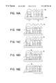
- FIG. 3 is a cross-sectional view illustrating a reflection type liquid crystal display in accordance with the first embodiment of the invention.
- FIG. 4 is a cross-sectional view illustrating a reflection type liquid crystal display in accordance with the second embodiment of the invention.
- FIG. 5 is a cross-sectional view illustrating a reflection type liquid crystal display in accordance with the third embodiment of the invention.
- FIG. 6 is a cross-sectional view illustrating a reflection type liquid crystal display in accordance with the fourth embodiment of the invention.
- FIG. 7 is a cross-sectional view illustrating a reflection type liquid crystal display in accordance with the seventh embodiment of the invention.
- FIG. 8 is a cross-sectional view illustrating a reflection type liquid crystal display in accordance with the eighth embodiment of the invention.
- FIG. 9 is a cross-sectional view illustrating a reflection type liquid crystal display in accordance with the ninth embodiment of the invention.
- FIG. 10 is a cross-sectional view illustrating a reflection type liquid crystal display in accordance with the tenth embodiment of the invention.
- FIG. 11 is a cross-sectional view illustrating a reflection type liquid crystal display in accordance with the eleventh embodiment of the invention.
- FIGS. 12A to 12 C are cross-sectional views of the reflection type liquid crystal display in accordance with the eleventh embodiment, illustrating respective steps of a method of fabricating the same.
- FIGS. 13A to 13 D are cross-sectional views of the reflection type liquid crystal display in accordance with the eleventh embodiment, illustrating respective steps of a method of fabricating the same.
- FIGS. 14A to 14 E are cross-sectional views of a reflection type liquid crystal display in accordance with a conventional method, illustrating respective steps of a method of fabricating the same.
- FIGS. 15A and 15B are cross-sectional views of a reflection type liquid crystal display including an insulating film composed of photosensitive material, illustrating respective steps of a method of fabricating the same.
- FIGS. 16A and 16E are cross-sectional views of a reflection type liquid crystal display including an insulating film composed of non-photosensitive material, illustrating respective steps of a method of fabricating the same.
- FIG. 17 is a cross-sectional view illustrating a reflection type liquid crystal display in accordance with the twelfth embodiment of the invention.
- FIGS. 18A to 18 F are cross-sectional views of a reflection type liquid crystal display in accordance with the thirteenth embodiment, illustrating respective steps of a method of fabricating the same.
- FIGS. 19A to 19 G are cross-sectional views of a reflection type liquid crystal display in accordance with the fourteenth embodiment, illustrating respective steps of a method of fabricating the same.
- FIGS. 20A to 20 F are cross-sectional views of a reflection type liquid crystal display in accordance with the fifteenth embodiment, illustrating respective steps of a method of fabricating the same.
- FIGS. 21A to 21 F are cross-sectional views of a reflection type liquid crystal display in accordance with example 1, illustrating respective steps of a method of fabricating the same.
- FIGS. 22A to 22 F are cross-sectional views of a reflection type liquid crystal display in accordance with example 2, illustrating respective steps of a method of fabricating the same.
- FIGS. 23A to 23 G are cross-sectional views of a reflection type liquid crystal display in accordance with example 3, illustrating respective steps of a method of fabricating the same.
- FIGS. 24A to 24 G are cross-sectional views of a reflection type liquid crystal display in accordance with example 4, illustrating respective steps of a method of fabricating the same.
- FIGS. 25A to 25 G are cross-sectional views of a reflection type liquid crystal display in accordance with example 5, illustrating respective steps of a method of fabricating the same.
- FIG. 3 is a cross-sectional view illustrating a reflection type liquid crystal display in accordance with the first embodiment of the invention.
- the reflection type liquid crystal display includes a thin film transistor having a forward stagger structure.
- the liquid crystal display 70 in accordance with the first embodiment is comprised of a lower substrate 72 A, an upper substrate 72 B in facing relation to the lower substrate 72 A, and a GH liquid crystal layer 14 sandwiched between the lower and upper substrates 72 A and 72 B.
- the lower substrate 72 A is comprised of an insulating substrate 35 A, an active matrix drive device 5 formed on the insulating substrate 35 A, a plurality of pillar-shaped projections 73 standing on the insulating substrate 35 A in line with the active matrix drive device 5 , a first insulating film 28 formed on top of the active matrix drive device 5 , a second insulating film 30 covering the active matrix drive device 5 and the pillar-shaped projections 73 therewith, and a light-reflective electrode plate 74 formed entirely over the second insulating film 30 and composed of metal having a high reflectance ratio.
- the active matrix drive device 5 is a thin film transistor having a forward stagger structure and comprised of a source electrode 21 formed on the insulating substrate 35 A, a drain electrode 22 formed on the insulating substrate 35 A, a semiconductor layer 19 , a doped layer 20 , an insulating layer 18 , and a metal layer 27 , the layers 19 , 20 , 18 and 27 being formed on the insulating substrate 35 A in this order.
- the first insulating file 28 is formed at a surface thereof with first raised and recessed portions 25 originated by the active matrix drive device 5 and the pillar-shaped projections 73 .
- the first raised and recessed portions 25 are designed to have a relatively great radius of curvature.
- the second insulating film 30 formed over the first insulating film 28 is also formed at a surface thereof with second raised and recessed portions 25 A.
- the first raised and recessed portions 25 are reflected in the second raised and recessed portions 25 A with respect to a shape.
- the second raised and recessed portions 25 A reflect and scatter incident light 15 .
- the light-reflective electrode plate 74 is electrically connected to the source electrode 21 of the thin film transistor 5 , and acts as both a reflective plate and a pixel electrode.
- the upper electrode 72 B is comprised of an insulating substrate 35 B, a color filter 3 formed on the insulating substrate 35 B, and a transparent electrode 4 formed over the color filter 3 .
- the transparent electrode 4 faces the lower substrate 72 A.
- the external lights 15 having passed through the upper substrate 72 B pass through the GH liquid crystal layer 14 , and are reflected at the second raised and recessed portions 25 A of the light-reflective electrode plate 74 in accordance with orientation which is dependent on a shape of the second raised and recessed portions 25 A.
- the thus reflected lights 16 pass again through the GH liquid crystal layer 14 and then the upper substrate 72 B. Thus, an operator can see the reflected lights 16 .
- the reflection type liquid crystal display 70 While the reflection type liquid crystal display 70 is in light-impermeable condition, the external lights 15 having passed through the upper substrate 72 B are all absorbed into the GH liquid crystal layer 14 before reaching the light-reflective electrode plate 74 . Accordingly, the external lights 15 do not pass through the upper electrode 72 B. As a result, the reflection type liquid crystal display 70 has a display screen with high contrast and high brightness.
- the second raised and recessed portions 25 A of the light-reflective electrode plate 74 can be formed by depositing the second insulating film 30 over the first insulating film 28 having the first raised and recessed portions 25 .
- the first raised and recessed portions 25 can be formed at the same time when the thin film transistor 5 is formed in photolithography and etching steps.
- the reflection type liquid crystal display 70 in accordance with the first embodiment can be fabricated in the less number of fabrication steps than the number of fabrication steps in a conventional method of fabricating a reflection type liquid crystal display.
- the projections 73 may be formed of at least one of the metal layer 27 , the gate insulating layer 18 , the semiconductor layer 19 , and the doped layer 20 , all of which have been formed when the thin film transistor 5 was fabricated on the insulating substrate 35 A, and the first insulating film 28 .
- the first insulating film 28 may not be formed.
- the second insulating film 30 may be formed directly covering the thin film transistor 5 therewith.
- FIG. 4 is a cross-sectional view illustrating a reflection type liquid crystal display in accordance with the second embodiment of the invention.
- the liquid crystal display 80 in accordance with the second embodiment is comprised of a lower substrate 72 A, an upper substrate 72 B in facing relation to the lower substrate 72 A, and a GH liquid crystal layer 14 sandwiched between the lower and upper substrates 72 A and 72 B.
- the insulating film 18 of the thin film transistor 5 is formed entirely over the insulating substrate 35 A.
- the lower substrate 72 A is comprised of an insulating substrate 35 A, an active matrix drive device 5 formed on the insulating substrate 35 A, a plurality of pillar-shaped projections 73 standing on the insulating film 18 in line with the active matrix drive device 5 , a first insulating film 28 formed on top of the active matrix drive device 5 , a second insulating film 30 covering the active matrix drive device 5 and the pillar-shaped projections 73 therewith, and a light-reflective electrode plate 74 formed entirely over the second insulating film.
- the active matrix drive device or thin film transistor 5 has a forward stagger structure and is comprised of a source electrode 21 formed on the insulating substrate 35 A, a drain electrode 22 formed on the insulating substrate 35 A, a semiconductor layer 19 and a doped layer 20 both formed on the insulating substrate 35 A between the source and drain electrodes 21 and 22 , the insulating layer 18 extending over the insulating substrate 35 A and hence covering the source electrode 21 , the drain electrode 22 , the semiconductor layer 19 , and the doped layer 20 therewith, and a gate electrode 17 formed on the insulating film 18 .
- the pillar-shaped projections 73 are comprised of the metal film 17 of which the gate electrode is formed, and the first insulating film 28 .
- the first insulating film 28 is formed at a surface thereof with first raised and recessed portions 25 originated by the active matrix drive device 5 and the pillar-shaped projections 73 .
- the second insulating film 30 formed over the first insulating film 28 is also formed at a surface thereof with second raised and recessed portions 25 A.
- the first raised and recessed portions 25 are reflected in the second raised and recessed portions 25 A with respect to a shape.
- the second raised and recessed portions 25 A reflect and scatter incident lights 15 .
- the projections 73 can be formed in photolithography and etching steps to be carried out for fabricating the thin film transistor 5 . That is, the projections 73 can be formed without addition of particular steps for forming them.
- FIG. 5 is a cross-sectional view illustrating a reflection type liquid crystal display in accordance with the third embodiment of the invention.
- a reflection type liquid crystal display 84 in accordance with the third embodiment is designed to include a reverse stagger type thin film transistor 7 as a switching device.
- the projections 73 can be formed in photolithography and etching steps to be carried out for fabricating the thin film transistor 7 .
- the third embodiment includes a different type of a switching device from the first and second embodiments, it is possible to form the projections 73 without addition of particular steps for forming them.
- each of the projections 73 is comprised of the layer of which the source electrode 21 and the drain electrode 22 are composed, and the first insulating film 28 .
- each of the projections 73 may be comprised of two or more layers among the layers constituting the thin film transistor 7 , and the first insulating film 28 .
- FIG. 6 is a cross-sectional view illustrating a reflection type liquid crystal display in accordance with the fourth embodiment of the invention.
- a reflection type liquid crystal display 86 in accordance with the fourth embodiment is designed to include a metal/insulator/metal (MIM) diode 71 as a switching device.
- MIM metal/insulator/metal
- the projections 73 can be formed in photolithography and etching steps to be carried out for fabricating MIM diode 71 .
- each of the projections 73 may be comprised of one or more layers among the layers constituting MIM diode 71 , and the first insulating film 28 .
- the projections 73 may be comprised of a layer or layers and the first insulating layer 28 formed on the layer or layers, unless the layer or layers constitute the switching device 5 , 7 or 71 . There is no limitation in combination in such layers.
- Each of the projections 73 is preferably designed to have a height in the range of 0.4 ⁇ m to 4 ⁇ m both inclusive. For instance, conditions for depositing the layers 17 , 18 , 19 and 20 , and the first insulating film 28 are controlled so that a total height of the layers 17 , 18 , 19 and 20 , and the first insulating film 28 is in the range of 0.4 ⁇ m to 4 ⁇ m both inclusive.
- the second insulating film 30 is preferably designed to have a height in the range of 0.6 ⁇ m to 4 ⁇ m both inclusive.
- the light-reflective plate 74 may be designed to overlap the switching device 5 , 7 or 71 through the second insulating film 30 to thereby enhance a numerical aperture.
- the first insulating film 28 may be composed of inorganic material or organic material.
- the first insulating film 28 may be formed by spin coating, printing, plasma-enhanced chemical vapor deposition (PCVD), thermal chemical vapor deposition, or sputtering.
- the first insulating film 28 is formed preferably by spin coating or printing, because those methods make it possible to vary a thickness of the first insulating film 28 more readily than a layer or layers constituting the switching device 5 , 7 or 71 by controlling viscosity of solvent, spin revolution per minute, and a roller speed.
- the first insulating film 28 may be composed preferably of polyimide resin, acrylate resin or SOG. This is because these resins make it easy to vary a thickness of the first insulating film 28 in a wide range, match well with materials used for fabricating the switching device 5 , 7 or 71 , and have superior characteristics such as electrical insulation, strength, adhesion, film stress, and stability.
- FIG. 7 is a cross-sectional view illustrating a reflection type liquid crystal display in accordance with the seventh embodiment of the invention.
- the first insulating film 28 in the reflection type liquid crystal display in accordance with the seventh embodiment is designed to have a tapered sidewall 38 .
- the reflection type liquid crystal display in accordance with the seventh embodiment has the same structure as the structure of the reflection type liquid crystal display in accordance with the first embodiment except the tapered sidewall 38 of the first insulating film 28 .
- the tapered sidewall 38 enables the second raised and recessed portions 25 A to have smooth inclination, which ensures enhancement in scattering characteristic of the light-reflective plate 74 .
- the reflection type liquid crystal display in accordance with the seventh embodiment can provide sufficient brightness on a display screen.
- FIG. 8 is a cross-sectional view illustrating a reflection type liquid crystal display in accordance with the eighth embodiment of the invention.
- the first insulating film 28 in the reflection type liquid crystal display in accordance with the eighth embodiment is designed to have a rounded summit 39 .
- the reflection type liquid crystal display in accordance with the eighth embodiment has the same structure as the structure of the reflection type liquid crystal display in accordance with the first embodiment except the rounded summit 39 of the first insulating film 28 .
- the first insulating film 28 is composed of thermally melting or thermally contracting, organic or inorganic material. By appropriately setting conditions for heating the first insulating film 28 , a summit of the first insulating film 28 is caused to become rounded.
- the rounded summit 39 of the first insulating film 28 makes it possible to readily control an inclination angle of the second raised and recessed portions 25 A of the light-reflective plate 74 .
- FIG. 9 is a cross-sectional view illustrating a reflection type liquid crystal display in accordance with the ninth embodiment of the invention.
- the reflection type liquid crystal display in accordance with the ninth embodiment is designed to include a reverse stagger type thin film transistor 7 as a switching device. Similarly to the reflection type liquid crystal display in accordance with the first embodiment, which is designed to include the forward stagger type thin film transistor 5 , the reflection type liquid crystal display in accordance with the ninth embodiment can provide enhanced brightness on a display screen.
- FIG. 10 is a cross-sectional view illustrating a reflection type liquid crystal display in accordance with the tenth embodiment of the invention.
- the reflection type liquid crystal display in accordance with the tenth embodiment is designed to include MIM diode 71 as a switching device. Similarly to the first embodiment including the forward stagger type thin film transistor 5 , the reflection type liquid crystal display in accordance with the tenth embodiment can provide enhanced brightness on a display screen.
- FIG. 11 is a cross-sectional view illustrating a reflection type liquid crystal display in accordance with the eleventh embodiment of the invention.
- the light-reflective electrode plate 74 is formed only above a region where the projections 73 are formed.
- the reflection type liquid crystal display in accordance with the eleventh embodiment has the same structure as the structure of the reflection type liquid crystal display in accordance with the eighth embodiment except the light-reflective electrode plate 74 formed in a limited region.
- the projections 73 are formed on the insulating substrate 35 A concurrently with the fabrication of the thin film transistor 5 , and the light-reflective electrode plate 74 is formed above the projections 73 with the second insulating film 30 being sandwiched therebetween. Since the light-reflective electrode plate 74 can be formed of a layer separate from layers of which the thin film transistor 5 , the source electrode 21 , and the drain electrode 22 are formed, the light-reflective electrode plate 74 could have an increased area, which would ensure an increase in light reflection.
- the first raised and recessed portions 25 are formed at a surface of the second insulating film 30 .
- the second insulating film 30 covering the projections 73 therewith would have no flat portions.
- An inclination angle of the second raised and recessed portions 25 A can be varied in a wide range by varying a dimension of the projections 73 and/or a thickness of the second insulating film 30 .
- the first insulating film 28 may be composed of insulating photosensitive material.
- FIGS. 12A to 12 C are cross-sectional views of the reflection type liquid crystal display including the first insulating film 28 composed of insulating photosensitive material, illustrating respective steps of a method of fabricating the same.
- the first insulating film 28 is formed over the layers 17 , 18 , 19 and 20 . Then, as illustrated in FIG. 12B, the first insulating film 28 is patterned by photolithography and etching. Then, as illustrated in FIG. 12C, the layers 17 , 18 , 19 and 20 are etched by using the patterned first insulating film 28 as a mask 50 , to thereby fabricate a switching device 41 along with the projections 73 .
- the patterned first insulating film 28 having been used as the mask 50 constitutes a part of the projections 73 .
- the reflection type liquid crystal display can be fabricated in the less number of fabrication steps.
- the first insulating film 28 may be composed of non-photosensitive material.
- FIGS. 13A to 13 D are cross-sectional views of the reflection type liquid crystal display including the first insulating film 28 composed of non-photosensitive material, illustrating respective steps of a method of fabricating the same.
- an insulating film 28 a is formed over the layers 17 , 18 , 19 and 20 .
- a layer 62 composed of photosensitive material is formed over the insulating film 28 a .
- the layer 62 is patterned by photolithography and etching.
- the layers 17 , 18 , 19 and 20 and the insulating film 28 a are etched by using the patterned insulating film 28 a as a mask, to thereby fabricate a switching device 41 together with the projections 73 .
- a combination of the layer 62 and the insulating film 28 acts as the first insulating film 28 shown in the previously mentioned embodiments.
- the patterned layer 62 having been used as a mask constitutes a part of the projections 73 .
- the reflection type liquid crystal display can be fabricated in the less number of fabrication steps.
- FIGS. 14A to 14 E are cross-sectional views of a reflection type liquid crystal display in accordance with a conventional method, illustrating respective steps of a method of fabricating the same.
- the illustrated method is a method using a photoresist film.
- the first insulating film 28 is formed over the layers 17 , 18 , 19 and 20 .
- a photoresist film 53 is formed over the first insulating film 28 .
- the photoresist film is patterned by photolithography and etching.
- the layers 17 , 18 , 19 and 20 and the first insulating film 28 are etched by using the patterned photoresist film 53 as a mask 50 , to thereby fabricate a switching device 41 together with the projections 73 .
- the mask 50 is removed.
- the conventional method illustrated in FIGS. 14A to 14 E additionally includes the steps of applying the photoresist film 53 , developing the photoresist film 53 , etching the layers 17 , 18 , 19 and 20 and the first insulating film 28 , and removing the photoresist film 53 , relative to the method illustrated in FIGS. 12A to 12 C or FIGS. 13A to 13 D.
- the conventional method cannot avoid having the greater number of fabrication steps than the number of fabrication steps of the methods illustrated in FIGS. 12A to 12 C or FIGS. 13A to 13 D.
- the second insulating film 30 may be composed of inorganic or organic material, similarly to the first insulating film 28 . It is preferable that the second insulating film 30 is an insulating film which can be formed by spin coating or printing.
- the second insulating film 30 is composed preferably of polyimide resin, acrylate resin, or SOG.
- the second insulating film 30 may be composed of insulating photosensitive material, similarly to the first insulating material 28 .
- the second insulating film 30 composed of non-photosensitive material is formed over the insulating substrate 35 A, covering the thin film transistor 5 and the projections 73 therewith.
- a photoresist film 53 is formed entirely over the second insulating film 30 .
- the photoresist film 53 is patterned by photolithography and dry etching steps.
- a contact hole 23 reaching the insulating substrate 35 A is formed throughout the second insulating film 30 through the use of the patterned photoresist film 53 as a mask.
- the photoresist film 53 is removed.
- FIGS. 15A and 15B are cross-sectional views of a reflection type liquid crystal display including the second insulating film 30 composed of insulating photosensitive material.
- the second insulating film 30 composed of photosensitive material is formed over the insulating substrate 35 A, covering the thin film transistor 5 and the projections 73 therewith. Then, as illustrated in FIG. 15B, a contact hole 23 reaching the insulating substrate 35 A is formed throughout the second insulating film 30 .
- the second insulating film 30 By composing the second insulating film 30 of photosensitive material, it is no longer necessary to carry out photolithography and etching steps for forming the contact hole 23 electrically connecting the switching device 5 to the light-reflective electrode plate 74 .
- the insulating substrates 35 A and 35 B may be composed of glass, organic material such as plastic and acryl, quartz, ceramics, and inorganic material such as silicon. As an alternative, semiconductor substrates may be used as the substrates 35 A and 35 B.
- FIG. 17 is a cross-sectional view illustrating a reflection type liquid crystal display in accordance with the twelfth embodiment of the invention.
- the upper substrate 72 B is designed to further include a polarizing plate 45 formed on a surface of the insulating substrate 35 B at the opposite side of the color filter 3 and the transparent electrode 4 , and a quarter wavelength plate 46 formed on the polarizing plate 45 .
- a liquid crystal layer is not to be limited to the GH liquid crystal layer 14 .
- a liquid crystal cell includes the switching device 41 and the light-reflective electrode plate 74 therein.
- the reflection type liquid crystal display in accordance with the twelfth embodiment is of single polarizing plate type.
- FIGS. 18A to 18 F are cross-sectional views of a reflection type liquid crystal display in accordance with the thirteenth embodiment, illustrating respective steps of a method of fabricating the same.
- the reflection type liquid crystal display in accordance with the thirteenth embodiment is fabricated concurrently with the fabrication of a thin film transistor having a forward stagger structure.
- photosensitive material and formed over the layers 17 , 18 , 19 and 20 is exposed to a light and developed for forming a pattern of the thin film transistor 5 and the projections 73 .
- the layers 17 , 18 , 19 and 20 are etched through the use of the thus patterned first insulating film 28 to thereby form the thin film transistor 5 and the projections 73 . That is, the thin film transistor 5 and the projections 73 are formed at the same time.
- the patterned first insulating film 28 having been used as a mask partially constitutes the projections 73 .
- the patterned first insulating film 28 having been used as a mask partially constitutes the projections 73 .
- the method of fabricating the reflection type liquid crystal display in accordance with the thirteenth embodiment carries out totally four photolithography and etching steps, whereas the conventional method as illustrated in FIGS. 2A to 2 H has to carry out totally seven photolithography and etching steps in order to fabricate the lower substrate 72 A.
- the thirteenth embodiment makes it possible to fabricate a reflection type liquid crystal display in the less number of photolithography and etching steps than the number of the same in the conventional method.
- the first and second insulating films 28 and 30 may be composed of inorganic photosensitive material in place of organic photosensitive material. The same advantages as mentioned above can be obtained.
- first and second insulating films 28 and 30 are composed of organic or inorganic non-photosensitive material, and are patterned in photolithography and etching steps, additional steps of applying a photoresist film
- the reflection type liquid crystal display in accordance with the present invention may include a forward stagger type thin film transistor, a reverse stagger type thin film transistor or MIM diode as an active matrix drive device.
- a forward stagger thin film transistor is preferably selected in order to maintain high performance of a switching device and reduce the number of fabrication steps.
- a metal film is deposited on the insulating substrate 35 A, and patterned into the source and drain electrodes 21 and 22 by first photolithography and etching steps.
- the doped layer 20 , the semiconductor layer 19 , the insulating film 18 , the gate insulating film 17 , and the first insulating film 28 are deposited on the insulating substrate 35 A.
- the first insulating film 28 is composed of organic photosensitive material.
- the first insulating film 28 is patterned into islands of the thin film transistor 5 and the projections 73 by second photolithography and etching steps.
- the layers 17 , 18 , 19 and 20 are etched with the patterned first insulating film 28 being used as a mask, to thereby form the thin film transistor 5 and the projections 73 .
- the second insulating film 30 is deposited entirely over the product resulted from the step illustrated in FIG. 18D, and thereafter, is patterned by third photolithography and etching steps to thereby form a contact hole 23 reaching the source electrode 21 .
- the thus formed second insulating film 30 is formed with the first raised and recessed portions 25 .
- a metal layer is deposited entirely over the product resulted from the step illustrated in FIG. 18 E.
- the metal layer is patterned by fourth photolithography and etching steps to thereby form the light-reflective electrode plate 74 over the second insulating film 30 .
- the first insulating film 28 composed of and removing the photoresist film have to be carried out. Even so, it is possible to reduce the number of fabrication steps relative to a conventional method of fabricating a reflection type liquid crystal display.
- the projections 73 are comprised of the layers 17 to 20 and the first insulating film 28 .
- the projections 73 may be formed of other combination of films.
- each of the projections 73 may be formed of at least one of the layers 17 to 20 , and the first insulating film 28 .
- each of the projections 73 may be formed of at least one of the layers 17 to 20 .
- the first raised and recessed portions 25 may be formed in any one of steps of patterning a layer, to be carried out in the fabrication of the thin film transistor 5 .
- the first insulating film 28 may be deposited on a metal film from which the source and drain electrodes 21 and 22 are to be formed, and be patterned concurrently with patterning the metal film into the source and drain electrodes 21 and 22 .
- FIGS. 19A to 19 G are cross-sectional views of a reflection type liquid crystal display in accordance with the fourteenth embodiment, illustrating respective steps of a method of fabricating the same.
- the reflection type liquid crystal display in accordance with the fourteenth embodiment is fabricated concurrently with the fabrication of a thin film transistor having a reverse stagger structure.
- a metal film is deposited on the insulating substrate 35 A, and patterned into the source and drain electrodes 21 and 22 by first photolithography and etching steps.
- the doped layer 20 , the semiconductor layer 19 , the insulating film 18 , the gate insulating film 17 , and the first insulating film 28 are deposited on the insulating substrate 35 A.
- the first insulating film 28 is composed of organic or inorganic photosensitive material.
- the first insulating film 28 is patterned into islands of the thin film transistor 5 and the projections 73 by second photolithography and etching steps.
- the islands of the patterned first insulating film 28 are rounded at a summit thereof
- the islands of the thin film transistor 5 and the projections 73 may be tapered at a sidewall thereof.
- the layers 17 , 18 , 19 and 20 are etched with the patterned first insulating film 28 being used as a mask, to thereby form the thin film transistor 5 and the projections 73 .
- the second insulating film 30 is deposited entirely over the product resulted from the step illustrated in FIG. 19E, and thereafter, is patterned by third photolithography and etching steps to thereby form a contact hole 23 reaching the source electrode 21 .
- the thus formed second insulating film 30 is formed with the first raised and recessed portions 25 .
- a metal layer is deposited entirely over the product resulted from the step illustrated in FIG. 19 F.
- the metal layer is patterned by fourth photolithography and etching steps to thereby form the light-reflective electrode plate 74 over the second insulating film 30 .
- the method of fabricating the reflection type liquid crystal display in accordance with the fourteenth embodiment carries out totally four photolithography and etching steps, whereas the conventional method as illustrated in FIGS. 2A to 2 H has to carry out totally seven photolithography and etching steps in order to fabricate the lower substrate 72 A.
- the fourteenth embodiment makes it possible to fabricate a reflection type liquid crystal display in the less number of photolithography and etching steps than the number of the same in the conventional method.
- the projections 73 are patterned in any one of steps of patterning a layer or layers constituting the thin film transistor 5 .
- the patterned first insulating film 28 having been used as a mask partially constitutes the projections 73 .
- the fourteenth embodiment includes the switching device 5 which is of different type of the switching device of the thirteenth embodiment, the fourteenth embodiment provides the same advantages as those obtained by the thirteenth embodiment.
- FIGS. 20A to 20 F are cross-sectional views of a reflection type liquid crystal display in accordance with the fifteenth embodiment, illustrating respective steps of a method of fabricating the same.
- the reflection type liquid crystal display in accordance with the fifteenth embodiment is fabricated concurrently with the fabrication of MIM diode 71 .
- a tantalum film is deposited on the insulating substrate 35 A, and patterned into a plurality of lead electrodes 68 by first photolithography and wet etching steps.
- tantalum oxide films 67 are formed around each of the lead electrodes 68 by anode oxidation. Then, a silicon dioxide film 56 is deposited entirely over the insulating substrate 35 A and the tantalum oxide films 67 . Then, a polyimide film 11 of which the first insulating film 28 is composed is deposited entirely over the silicon dioxide film 56 .
- the polyimide film 11 and the silicon dioxide film 56 are patterned by second photolithography and dry etching steps to thereby form islands of MIM diode 71 and the projections 73 .
- each of the islands are rounded at summits thereof by melting the islands.
- the islands of the thin film transistor 5 and the projections 73 may be tapered at a sidewall thereof.
- a polyimide film 11 of which the second insulating film 30 is composed is deposited entirely over the product resulted from the step illustrated in FIG. 20 D.
- the polyimide film 11 is patterned by third photolithography and etching steps to thereby form a contact hole 23 reaching the silicon dioxide film 56 .
- the thus formed second insulating film 30 is formed with the first raised and recessed portions 25 .
- an aluminum layer is deposited entirely over the product resulted from the step illustrated in FIG. 20 E.
- the aluminum layer is patterned by fourth photolithography and wet etching steps to thereby form the light-reflective electrode plate 74 over the second insulating film 30 .
- the method of fabricating the reflection type liquid crystal display in accordance with the fifteenth embodiment carries out totally four photolithography and etching steps, whereas the conventional method as illustrated in FIGS. 2A to 2 H has to carry out totally seven photolithography and etching steps in order to fabricate the lower substrate 72 A.
- the fifteenth embodiment makes it possible to fabricate a reflection type liquid crystal display in the less number of photolithography and etching steps than the number of the same in the conventional method.
- the resultant reflection type liquid crystal display provide enhanced brightness and contrast.
- FIGS. 21A to 21 F are cross-sectional views of a reflection type liquid crystal display in accordance with example 1, illustrating respective steps of a method of fabricating the same.
- the reflection type liquid crystal display in accordance with example 1 is fabricated concurrently with the fabrication of a thin film transistor having a forward stagger structure.
- a chromium film is deposited on the insulating substrate 35 A by a thickness of 50 nm by sputtering. Then, the chromium film is patterned into the source and drain electrodes 21 and 22 by first photolithography and etching steps.
- a 100 nm-thick doped layer 20 , a 100 nm-thick semiconductor layer 19 , and a 400 nm-thick gate insulating film 18 are deposited on the insulating substrate 35 A by plasma-enhanced chemical vapor deposition.
- the gate insulating film 18 is composed of a silicon dioxide film and a silicon nitride film.
- the semiconductor layer 19 is composed of amorphous silicon, and the doped layer 20 is composed of n-type amorphous silicon.
- the conditions for forming the silicon dioxide film by plasma-enhanced chemical vapor deposition are as follows.
- Film deposition temperature 200-300 degrees centigrade
- Plasma power 200 W
- the conditions for forming the silicon nitride film by plasma-enhanced chemical vapor deposition are as follows.
- Plasma power 200 W
- the conditions for forming the amorphous silicon film by plasma-enhanced chemical vapor deposition are as follows.
- Plasma power 50 W
- the conditions for forming the n-type amorphous silicon film by plasma-enhanced chemical vapor deposition are as follows.
- Plasma power 50 W
- a chromium film 52 is deposited by a thickness of 50 nm by sputtering entirely over the gate insulating film 18 .
- an organic insulating film 33 from which the first insulating film 28 is formed is deposited by a thickness of 2 ⁇ m by spin coating entirely over the chromium film 52 .
- the organic insulating film 33 is comprised of a polyimide film commercially available from Nissan Kagaku Co. in the tradename of “RN-812”, and a resist film deposited on the polyimide film. The resist film is used for patterning the polyimide film.
- the conditions for forming the polyimide film are as follows.
- Pre-baking temperature 90 degrees centigrade
- the conditions for forming the resist film are as follows.
- Pre-baking temperature 90 degrees centigrade
- the resist film is patterned by exposure to a light and development, and then, is post-baked at 90 degrees centigrade for 30 minutes. Then, the organic insulating film 33 is formed with the first raised and recessed portions 25 by dry etching, using the patterned resist film as a mask.
- the conditions for dry etching the polyimide film are as follows.
- Etching gases fluorine tetrachloride gas and oxygen gas
- Plasma power 100-300 W
- a photoresist film 53 is deposited entirely over the thus formed first insulating film 28 .
- the photoresist film 53 is patterned into a pattern for forming the thin film transistor 5 and the projections 73 , by second photolithography and etching steps.
- the first insulating layer 28 , the chromium film 52 , the gate insulating film 18 , the semiconductor layer 19 , and the doped layer 20 are etched with the patterned photoresist film 53 being used as a mask.
- the chromium film 52 is wet etched, and the silicon dioxide film and silicon nitride film both cooperating to each other to thereby form the gate insulating film 18 , and the amorphous silicon layer constituting the semiconductor layer 19 are dry etched.
- An aqueous solution containing perchloric hydroacid and cerium (II) nitrate ammonium is used for wet etching the chromium film 52 .
- the conditions for dry etching the silicon dioxide film and the silicon nitride film are as follows.
- Etching gases fluorine tetrachloride gas and oxygen gas
- Plasma power 100-300 W
- the conditions for dry etching the amorphous silicon film are as follows.
- Etching gases chlorine gas and oxygen gas
- Plasma power 50-200 W
- the thus formed thin film transistor 5 and the projections 73 have random cross-sections.
- a maximum height of the thin film transistor 5 and the projections 73 is equal to 3.7 ⁇ m, which is a sum of a thickness of 700 nm of the thin film transistor 5 , a thickness of 2 ⁇ m of the first insulating film 28 , and a thickness of 1 ⁇ m of the photoresist film 53 .
- the photoresist film 53 having been used as a mask remains as it is without removal, and constitute a part of the projections 73 . Hence, the process is simplified relative to a conventional process.
- a 2 ⁇ m-thick polyimide film 30 from which the second insulating film 30 is composed is deposited entirely over the product resulted from the step illustrated in FIG. 21 D.
- the polyimide film 30 is composed of polyimide commercially available from Nissan Kagaku Co. in the tradename of “RN-812”.
- the conditions for applying the polyimide film 30 are as follows.
- Pre-baking temperature 90 degrees centigrade
- Spin revolution per minute may be set 120 r.p.m. by varying various parameters.
- the polyimide film 30 is patterned by third photolithography and etching steps to thereby form a contact hole 23 reaching the source electrode 21 .
- the thus formed second insulating film 30 is formed with the first raised and recessed portions 25 .
- the conditions for dry etching the polyimide film 30 are the same as the above-mentioned conditions for etching the polyimide film from which the first insulating film 28 is composed.
- an aluminum layer is deposited by a thickness of 300 nm by sputtering entirely over the product resulted from the step illustrated in FIG. 21 E.
- the aluminum layer is patterned by fourth photolithography and etching steps to thereby form the light-reflective electrode plate 74 over the second insulating film 30 .
- the aluminum film is wet etched in etchant heated up to 60 degrees centigrade and containing phosphoric acid, acetic acid, and nitric acid.
- the light-reflective electrode plate 74 is formed so as to have a numerical aperture of 80%.
- the lower and upper substrates 72 A and 72 B are designed to include alignment films. Thereafter, the lower substrate 72 A and the upper substrate 72 B on which the transparent electrode 4 composed of indium-tin-oxide (ITO) are adhered to each other by applying epoxy adhesive to a marginal area of the substrates 72 A and 72 B so that the layers formed on each of the substrates 72 A and 72 B face to each other.
- the substrates 72 A and 72 B are spaced away from each other by sandwiching spacers such as plastic particles therebetween.
- GH liquid crystal is introduced into a space formed between the substrates 72 A and 72 B. Thus, there is completed a liquid crystal display.
- the light-reflective electrode plate 74 has uniform reflection characteristic including superior light-scattering characteristic.
- the reflection type liquid crystal display in accordance with example 1 provides white display which is brighter than newspaper.
- a reflection type liquid crystal display having superior display characteristic can be accomplished at low costs.
- a color reflection type liquid crystal display can be also accomplished at low costs by providing an RGB color filter on the upper substrate 72 B.
- the projections 73 are patterned in any one of steps of patterning a layer or layers constituting the thin film transistor 5 .
- the patterned photoresist film 53 having been used as a mask partially constitutes the projections 73 .
- the method of fabricating the reflection type liquid crystal display in accordance with example 1 carries out totally four photolithography and etching steps, which is smaller in number than the conventional method.
- a height of the projections 73 is not to be limited to the above-mentioned range.
- a height of the projections 73 can be controlled by varying thicknesses of the layers 17 to 20 and the first insulating film 28 .
- a thickness of the first insulating film 28 composed of organic or inorganic material can be varied in wider range than a thickness of the thin film transistor 5 comprised of the layers 17 to 22 .
- orientation in performance of the light-reflective electrode plate 74 can be varied by varying a height of the projections 73 .
- each of the projections 73 is comprised of the chromium film, the silicon dioxide film, the silicon nitride film, the amorphous silicon film, the n-type amorphous silicon film, the chromium film, and the first insulating film 28 .
- the projections 73 may be comprised of other combination of films. There are a couple of possible combinations. Hence, a height of the projections 73 can be varied without addition of steps for doing so.
- the first insulating film 28 is comprised of a polyimide film in example 1, material of which the first insulating film 28 is formed is not to be limited to polyimide.
- the first insulating film 28 may be composed of silica such as one commercially available from Tore in the tradename of “PSB”, acrylate resin such as one commercially available from Nippon Gosei Gomu in the tradename of “MFR 305”, or SOG such as one commercially available from Sumitomo Kagaku in the tradename of “SF 9214”.
- each of the projections 73 is comprised of the chromium film, the silicon dioxide film, the silicon nitride film, the amorphous silicon film, the n-type amorphous silicon film, the chromium film, and the first insulating film 28 .
- the projections 73 may be comprised of any one the following combinations:
- a chromium film an n-type amorphous silicon film, an amorphous silicon film, a silicon nitride film, a silicon dioxide film, a silicon nitride film, and a chromium film;
- a chromium film an n-type amorphous silicon film, an amorphous silicon film, a silicon nitride film, a silicon dioxide film, a silicon nitride film, a chromium film, and the first insulating film 28 composed of organic material.
- the projections 73 By composing the projections 73 of any one of the above-mentioned combinations, it is possible to provide better light-scattering characteristic to the light-reflective electrode plate 74 .
- the projections 73 can be tapered at a sidewall thereof by varying photolithography conditions, ensuring enhanced light-scattering characteristic of the light-reflective electrode plate 74 .
- Example 2 is the same as the above-mentioned example 1 except that the first insulating film 28 and the second insulating film 30 are both composed of photosensitive material.
- FIGS. 22A to 22 F are cross-sectional views of a reflection type liquid crystal display in accordance with example 2, illustrating respective steps of a method of fabricating the same.
- the reflection type liquid crystal display in accordance with example 2 is fabricated concurrently with the fabrication of a thin film transistor having a forward stagger structure.
- a chromium film is deposited on the insulating substrate 35 A by sputtering. Then, the chromium film is patterned into the source and drain electrodes 21 and 22 by first photolithography and wet etching steps.
- a doped layer 20 , a semiconductor layer 19 , and a gate insulating film 18 are deposited on the insulating substrate 35 A by plasma-enhanced chemical vapor deposition.
- the gate insulating film 18 is composed of a silicon dioxide film and a silicon nitride film.
- the semiconductor layer 19 is composed of amorphous silicon, and the doped layer 20 is composed of n-type amorphous silicon.
- a chromium film 17 from which a gate electrode is formed is deposited by sputtering entirely over the gate insulating film 18 .
- a photosensitive insulating film 28 from which the first insulating film 28 is formed is deposited by spin coating entirely over the chromium film 17 .
- the first insulating film 28 is patterned into a pattern for forming the thin film transistor 5 and the projections 73 , by second photolithography and etching steps.
- the chromium film 17 , the gate insulating film 18 , the semiconductor layer 19 , and the doped layer 20 are dry etched with the patterned first insulating film 28 being used as a mask.
- a photosensitive insulating film 30 from which the second insulating film 30 is formed is deposited entirely over the product resulted from the step illustrated in FIG. 22 D.
- the second insulating film 30 is patterned by third photolithography and etching steps to thereby form a contact hole 23 reaching the source electrode 21 .
- the thus formed second insulating film 30 is formed with the first raised and recessed portions 25 .
- an aluminum layer is deposited by sputtering entirely over the product resulted from the step illustrated in FIG. 22 E.
- the aluminum layer is patterned by fourth photolithography and etching steps to thereby form the light-reflective electrode plate 74 over the second insulating film 30 .
- the lower substrate 72 A of the reflection type liquid crystal display can be fabricated by carrying out four photolithography and etching steps.
- the first and second insulating films 28 and 30 are composed of photosensitive material. For these reasons, it is no longer necessary to carry out a step of removing a photoresist film after patterning the layers, which ensures the less number of fabrication steps than the conventional method.
- the photosensitive insulating layer from which the first and second insulating films 28 and 30 are formed is commercially available from Tokyo Ouka in the tradename of “OFPR 800”.
- Other photosensitive insulating layers may be used for forming the first and second insulating films 28 and 30 , regardless of whether they are organic or inorganic.
- Example 3 is different from the above-mentioned example 2 in that the first insulating film 28 is composed of organic or inorganic insulating material which can be thermally melted, and that the first insulating film 28 is tapered at a sidewall thereof and further rounded at a summit thereof.
- FIGS. 23A to 23 G are cross-sectional views of a reflection type liquid crystal display in accordance with example 3, illustrating respective steps of a method of fabricating the same.
- the method illustrated in FIGS. 23A to 23 G is different from the method illustrated in FIGS. 22A to 22 F only in additionally including the step illustrated in FIG. 23 D. That is, after the first insulating film 28 has been patterned, as illustrated in FIG. 23C, the patterned first insulating film 28 is burned at 200 degrees centigrade to thereby taper a sidewall of the first insulating film 28 and make a summit of the first insulating film 28 rounded.
- the number of photolithography steps for fabricating the lower substrate 72 A of a reflection type liquid crystal display is four, similarly to the above-mentioned examples 1 and 2.
- the first insulating film 28 is composed of material having thermally melting characteristic, a summit of the first insulating film 28 can be made rounded to thereby reduce an area of flat portions, by appropriately setting a burning temperature, resulting in reduction in regular reflection and hence enhancement in reflection ability.
- the first insulating film 28 is composed of material commercially available from Tokyo Ouka in the tradename of “TMR-P3”.
- the first insulating film 28 may be composed of material commercially available from Tokyo Ouka in the tradename of “OFPR-800”.
- the first insulating film 28 After the first insulating film 28 has been patterned, the first insulating film 28 is heated at 200 degrees centigrade for 10 minutes, for instance. Irregularity formed at a summit of the first insulating film 28 (see FIG. 23C) in the thin film transistor 5 is melted, and as a result, a summit of the first insulating film 28 is turned to be rounded, as illustrated in FIG. 23 D.
- the light-reflected electrode plate 74 having desired reflection characteristic by controlling a shape, arrangement, and fabrication conditions of the thin film transistor 5 and the projections 73 .
- the fabrication conditions include thicknesses of layers, pre-burning temperature, location, size, post-burning temperature, and burning time.
- a reflection type liquid crystal display having the same display performance as example 3 can be accomplished by tapering the first insulating film 28 at a sidewall thereof
- a taper angle of a sidewall of the first insulating film 28 can be controlled by varying conditions of exposure and development in a photolithography and etching step.
- FIGS. 24A to 24 G are cross-sectional views of a reflection type liquid crystal display in accordance with example 4, illustrating respective steps of a method of fabricating the same.
- the reflection type liquid crystal display in accordance with example 4 is fabricated concurrently with the fabrication of a thin film transistor having a forward stagger structure.
- a chromium film is deposited on the insulating substrate 35 A by sputtering. Then, the chromium film is patterned into the source and drain electrodes 21 and 22 by first photolithography and etching steps.
- a doped layer 20 , a semiconductor layer 19 , and a gate insulating film 18 are deposited on the insulating substrate 35 A by plasma-enhanced chemical vapor deposition.
- the gate insulating film 18 is composed of a silicon nitride film.
- the semiconductor layer 19 is composed of amorphous silicon, and the doped layer 20 is composed of n-type amorphous silicon.
- the layers 18 to 20 are patterned into an island 49 by second photolithography and etching steps.
- a silicon nitride film 56 , a chromium film 52 , and a first photosensitive insulating film 28 from which the first insulating film 28 is formed are deposited in this order over the product illustrated in FIG. 24 B.
- the first photosensitive insulating film 28 is patterned into a pattern of the thin film transistor 5 and the projections 73 by third photolithography and etching steps, as illustrated in FIG. 24 D.
- the chromium film 52 is etched with the thus patterned first photosensitive insulating film 28 being used as a mask, to thereby form a gate electrode of the thin film transistor 5 , and the projections 73 .
- a polyimide film 30 from which the second insulating film 30 is composed is deposited entirely over the product resulted from the step illustrated in FIG. 24 E.
- the polyimide film 30 is patterned by fourth photolithography and etching steps to thereby form a contact hole 23 reaching the source electrode 21 .
- the thus formed second insulating film 30 is formed with the first raised and recessed portions 25 .
- an aluminum layer is deposited by sputtering entirely over the product resulted from the step illustrated in FIG. 24 F.
- the aluminum layer is patterned by fifth photolithography and etching steps to thereby form the light-reflective electrode plate 74 over the second insulating film 30 .
- the lower substrate 72 A and the upper substrate 72 B are adhered to each other by applying epoxy adhesive to a marginal area of the substrates 72 A and 72 B so that the layers formed on each of the substrates 72 A and 72 B face to each other.
- the substrates 72 A and 72 B are spaced away from each other by sandwiching spacers such as plastic particles therebetween.
- GH liquid crystal is introduced into a space formed between the substrates 72 A and 72 B.
- the number of photolithography and etching steps necessary for fabricating the reflection type liquid crystal display in accordance with the above-mentioned example 4 is five.
- Materials of which the layers constituting the thin film transistor 5 are composed are not to be limited to the above-mentioned materials.
- the layers constituting the thin film transistor 5 may be composed of other materials.
- first and second insulating films 28 and 30 are composed of polyimide in example 4, they may be composed of other organic or inorganic insulating materials.
- the first insulating film 28 may be composed of material which is thermally melted, in which case, a summit of the first insulating film 28 can be made rounded, ensuring the first raised and recessed portions 25 would have a smooth surface with the result that the light-reflective electrode plate 74 could have improved light-scattering characteristic.
- FIGS. 25A to 25 G are cross-sectional views of a reflection type liquid crystal display in accordance with example 5, illustrating respective steps of a method of fabricating the same.
- the reflection type liquid crystal display in accordance with example 5 is fabricated concurrently with the fabrication of a thin film transistor having a reverse stagger structure.
- a metal film is deposited on the insulating substrate 35 A. Then, the metal film is patterned into a gate electrode 17 by first photolithography and etching steps.
- a doped layer 20 , a semiconductor layer 19 , and a gate insulating film 18 are deposited on the insulating substrate 35 A by plasma-enhanced chemical vapor deposition.
- the layers 19 and 20 are patterned into an island 49 by second photolithography and etching steps, as illustrated in FIG. 25 C.
- a metal film 27 and an organic or inorganic insulating film 28 from which the first insulating film 28 is formed are deposited entirely over the product illustrated in FIG. 25 C.
- the first insulating film 28 is patterned into a pattern of the thin film transistor 5 and the projections 73 by third photolithography and etching steps.
- the metal film 27 is etched with the thus patterned first insulating film 28 being used as a mask, to thereby form source and drain electrodes of the thin film transistor 5 , and the projections 73 .
- an organic or inorganic insulating film 30 from which the second insulating film 30 is formed is deposited entirely over the product resulted from the step illustrated in FIG. 25 E.
- the second insulating film 30 is patterned by fourth photolithography and etching steps to thereby form a contact hole 23 reaching the source electrode.
- the thus formed second insulating film 30 is formed with the first raised and recessed portions 25 .
- an aluminum layer is deposited by sputtering entirely over the product resulted from the step illustrated in FIG. 25 F.
- the aluminum layer is patterned by fifth photolithography and etching steps to thereby form the light-reflective electrode plate 74 over the second insulating film 30 , as illustrated in FIG. 25 G.
- the number of photolithography and etching steps necessary for fabricating the reflection type liquid crystal display in accordance with the above-mentioned example 5 is five, whereas the number of the same in a conventional method is six. Hence, the method of fabricating the reflection type liquid crystal display in accordance with example 5 can be simplified relative to a conventional one.
Abstract
Description
Claims (27)
Applications Claiming Priority (2)
| Application Number | Priority Date | Filing Date | Title |
|---|---|---|---|
| JP10-059475 | 1998-03-11 | ||
| JP10059475A JP3019831B2 (en) | 1998-03-11 | 1998-03-11 | Reflective liquid crystal display device and method of manufacturing the same |
Publications (1)
| Publication Number | Publication Date |
|---|---|
| US6407784B1 true US6407784B1 (en) | 2002-06-18 |
Family
ID=13114378
Family Applications (1)
| Application Number | Title | Priority Date | Filing Date |
|---|---|---|---|
| US09/281,073 Expired - Lifetime US6407784B1 (en) | 1998-03-11 | 1999-03-09 | Reflection type liquid crystal display and method of fabricating the same |
Country Status (3)
| Country | Link |
|---|---|
| US (1) | US6407784B1 (en) |
| JP (1) | JP3019831B2 (en) |
| KR (1) | KR100305628B1 (en) |
Cited By (30)
| Publication number | Priority date | Publication date | Assignee | Title |
|---|---|---|---|---|
| US20020051107A1 (en) * | 2000-10-31 | 2002-05-02 | Kohei Nagayama | Liquid crystal display device |
| US20020075423A1 (en) * | 2000-09-14 | 2002-06-20 | Masahiro Fujino | Reflective liquid crystal display device |
| US6509943B2 (en) * | 2000-02-12 | 2003-01-21 | Lg. Philips Lcd Co., Ltd. | Reflective liquid crystal display device |
| US20030164915A1 (en) * | 2002-03-01 | 2003-09-04 | Sayuri Fujiwara | Display device and method for fabricating the display device |
| WO2003079107A1 (en) * | 2002-03-19 | 2003-09-25 | Koninklijke Philips Electronics N.V. | Semiconductor device manufacturing method, semiconductor device, and liquid crystal display |
| US20040125287A1 (en) * | 2002-12-31 | 2004-07-01 | Jang Sang Min | Reflective plate of LCD and fabrication method thereof |
| US20040145689A1 (en) * | 2002-12-17 | 2004-07-29 | Fujitsu Display Technologies Corporation | Liquid crystal display device and method of manufacturing the same |
| US6781759B1 (en) * | 1999-10-21 | 2004-08-24 | Matsushita Electric Industrial Co., Ltd. | Reflector, production method thereof, display element, and display device |
| US20040196419A1 (en) * | 2000-01-21 | 2004-10-07 | Nec Corporation | Reflection-type liquid crystal display and method for manufacturing the same |
| US20040223107A1 (en) * | 2000-12-07 | 2004-11-11 | Hitachi, Ltd. | Liquid crystal display device |
| US6836305B1 (en) * | 1998-07-15 | 2004-12-28 | Hitachi, Ltd. | Reflection-type, liquid crystal display device and process for producing the same |
| US20050029517A1 (en) * | 2001-07-09 | 2005-02-10 | Naoki Sumi | Method of forming a reflective electrode and a liquid crystal display device |
| US20050052597A1 (en) * | 2000-01-14 | 2005-03-10 | Nec Corporation | Reflective liquid crystal display apparatus and production method thereof |
| US20050140838A1 (en) * | 2003-12-29 | 2005-06-30 | Eui Seok Oh | Array substrate for transflective liquid crystal display device and method for manufacturing the same |
| US6972821B2 (en) * | 2001-05-14 | 2005-12-06 | Nec Lcd Technologies, Ltd. | Active-matrix addressing liquid-crystal display device and method of fabricating same |
| US20060197883A1 (en) * | 2002-03-01 | 2006-09-07 | Semiconductor Energy Laboratory Co., Ltd. | Liquid Crystal Display Device |
| US20070126959A1 (en) * | 2002-03-01 | 2007-06-07 | Semiconductor Energy Laboratory Co., Ltd. | Liquid Crystal Display Device |
| CN100356258C (en) * | 2003-12-30 | 2007-12-19 | 中芯国际集成电路制造(上海)有限公司 | Method for making metallic reflective layer of silicon based LCD device |
| US20090033818A1 (en) * | 1999-08-12 | 2009-02-05 | Semiconductor Energy Laboratory Co., Ltd. | Semiconductor Device and Method of Manufacturing the Semiconductor Device |
| US20090195741A1 (en) * | 2006-06-30 | 2009-08-06 | Yoshihito Hara | Liquid crystal display and method for manufacturing liquid crystal display |
| US20100014031A1 (en) * | 2006-12-14 | 2010-01-21 | Tetsuo Kikuchi | Liquid crystal display device and process for producing liquid crystal display device |
| US20100045885A1 (en) * | 2007-01-24 | 2010-02-25 | Hajime Imai | Liquid crystal display device |
| US20100053517A1 (en) * | 2007-04-13 | 2010-03-04 | Hajime Imai | Liquid crystal display and method of manufacturing liquid crystal display |
| US20100118238A1 (en) * | 2007-01-31 | 2010-05-13 | Junya Shimada | Liquid crystal display device |
| US20100182527A1 (en) * | 2007-06-26 | 2010-07-22 | Tetsuo Kikuchi | Liquid crystal display device and method of manufacturing liquid crystal display device |
| US20100315578A1 (en) * | 2006-10-18 | 2010-12-16 | Yoshihito Hara | Liquid crystal display and method for manufacturing liquid crystal display |
| US20110012815A1 (en) * | 2008-03-31 | 2011-01-20 | Toshihide Tsubata | Active matrix substrate, liquid crystal panel, liquid crystal display device, liquid crystal display unit, and television receiver |
| US20110147752A1 (en) * | 2000-05-09 | 2011-06-23 | Semiconductor Energy Laboratory Co., Ltd. | Semiconductor device and manufacturing method thereof |
| US8586988B2 (en) | 2000-03-08 | 2013-11-19 | Semiconductor Energy Laboratory Co., Ltd. | Semiconductor device and manufacturing method thereof |
| US11397348B2 (en) * | 2017-05-23 | 2022-07-26 | Beijing Boe Optoelectronics Technology Co., Ltd. | Array substrate having convex component, method for fabricating the same, liquid crystal display panel, and display device |
Families Citing this family (18)
| Publication number | Priority date | Publication date | Assignee | Title |
|---|---|---|---|---|
| JP4118484B2 (en) | 2000-03-06 | 2008-07-16 | 株式会社半導体エネルギー研究所 | Method for manufacturing semiconductor device |
| JP4700160B2 (en) | 2000-03-13 | 2011-06-15 | 株式会社半導体エネルギー研究所 | Semiconductor device |
| JP4118485B2 (en) | 2000-03-13 | 2008-07-16 | 株式会社半導体エネルギー研究所 | Method for manufacturing semiconductor device |
| JP4683688B2 (en) | 2000-03-16 | 2011-05-18 | 株式会社半導体エネルギー研究所 | Method for manufacturing liquid crystal display device |
| US6747289B2 (en) * | 2000-04-27 | 2004-06-08 | Semiconductor Energy Laboratory Co., Ltd. | Semiconductor device and method of fabricating thereof |
| JP5057613B2 (en) * | 2000-04-27 | 2012-10-24 | 株式会社半導体エネルギー研究所 | Semiconductor device and electronic equipment |
| JP3365409B2 (en) | 2000-11-08 | 2003-01-14 | 日本電気株式会社 | Reflector, reflection type liquid crystal display device and method for manufacturing the same |
| JP4632522B2 (en) * | 2000-11-30 | 2011-02-16 | Nec液晶テクノロジー株式会社 | Method for manufacturing reflective liquid crystal display device |
| KR100392602B1 (en) * | 2000-12-29 | 2003-07-28 | 엘지.필립스 엘시디 주식회사 | Array Panel used for a Liquid Crystal Display Device and Method of Fabricating the same |
| US7071037B2 (en) | 2001-03-06 | 2006-07-04 | Semiconductor Energy Laboratory Co., Ltd. | Semiconductor device and manufacturing method thereof |
| JP5165169B2 (en) * | 2001-03-07 | 2013-03-21 | 株式会社ジャパンディスプレイイースト | Liquid crystal display |
| KR100924749B1 (en) * | 2002-09-12 | 2009-11-06 | 엘지디스플레이 주식회사 | An substrate for LCD and method for fabricating the same |
| KR100939616B1 (en) | 2002-12-31 | 2010-02-01 | 엘지디스플레이 주식회사 | Reflecting layer and its fabrication method of reflective layer for reflective type liquid crystal display |
| JP4610552B2 (en) * | 2003-06-04 | 2011-01-12 | ティーピーオー、ホンコン、ホールディング、リミテッド | Manufacturing method of liquid crystal display device |
| JP4845531B2 (en) | 2006-02-28 | 2011-12-28 | 三菱電機株式会社 | Image display device |
| JP4668247B2 (en) * | 2007-07-26 | 2011-04-13 | 三菱電機株式会社 | Manufacturing method of liquid crystal display device |
| JP2011118422A (en) * | 2011-03-01 | 2011-06-16 | Nec Lcd Technologies Ltd | Liquid crystal display device, thin film transistor array substrate for liquid crystal display device, and method for manufacturing the substrate |
| CN115298600B (en) * | 2020-12-25 | 2023-10-20 | 京东方科技集团股份有限公司 | Display panel, manufacturing method of display panel and display device |
Citations (12)
| Publication number | Priority date | Publication date | Assignee | Title |
|---|---|---|---|---|
| JPS5971081A (en) | 1982-10-18 | 1984-04-21 | 株式会社東芝 | Liquid crystal display and manufacture thereof |
| JPS616390A (en) | 1984-05-01 | 1986-01-13 | ジエイダブリユ−アイ・リミテツド | Cloth for dryer having yarn strand prepared from melt extrudable polyphenylene sulfide |
| JPH0611711A (en) | 1992-06-26 | 1994-01-21 | Sharp Corp | Reflection type liquid crystal display device |
| JPH0627481A (en) | 1992-07-10 | 1994-02-04 | Sharp Corp | Reflective active matrix substrate, its production and liquid crystal display device |
| JPH0675238A (en) | 1991-09-10 | 1994-03-18 | Sharp Corp | Reflection-type liquid crystal display device and its production |
| JPH0675237A (en) | 1992-08-28 | 1994-03-18 | Sharp Corp | Reflection-type liquid crystal display device |
| JPH06273800A (en) | 1993-03-24 | 1994-09-30 | Sharp Corp | Reflection type liquid crystal display device |
| JPH06342153A (en) | 1993-06-02 | 1994-12-13 | Sharp Corp | Reflection type liquid crystal display device and formation of the same |
| JPH0954318A (en) * | 1995-08-16 | 1997-02-25 | Nec Corp | Reflection type liquid crystal display device and its production |
| US5691791A (en) * | 1993-07-30 | 1997-11-25 | Sharp Kabushiki Kaisha | Reflective liquid crystal display device and reflector |
| US5805252A (en) * | 1994-10-03 | 1998-09-08 | Sharp Kabushiki Kaisha | Reflection type liquid crystal display and method of producing the same |
| US6097458A (en) * | 1995-12-11 | 2000-08-01 | Sharp Kabushiki Kaisha | Reflector, reflective liquid crystal display incorporating the same and method for fabricating the same |
Family Cites Families (1)
| Publication number | Priority date | Publication date | Assignee | Title |
|---|---|---|---|---|
| JPH05173158A (en) * | 1991-12-26 | 1993-07-13 | Sharp Corp | Reflection type liquid crystal display device and its manufacture |
-
1998
- 1998-03-11 JP JP10059475A patent/JP3019831B2/en not_active Expired - Lifetime
-
1999
- 1999-03-09 US US09/281,073 patent/US6407784B1/en not_active Expired - Lifetime
- 1999-03-11 KR KR1019990008118A patent/KR100305628B1/en not_active IP Right Cessation
Patent Citations (14)
| Publication number | Priority date | Publication date | Assignee | Title |
|---|---|---|---|---|
| JPS5971081A (en) | 1982-10-18 | 1984-04-21 | 株式会社東芝 | Liquid crystal display and manufacture thereof |
| JPS616390A (en) | 1984-05-01 | 1986-01-13 | ジエイダブリユ−アイ・リミテツド | Cloth for dryer having yarn strand prepared from melt extrudable polyphenylene sulfide |
| JPH0675238A (en) | 1991-09-10 | 1994-03-18 | Sharp Corp | Reflection-type liquid crystal display device and its production |
| JPH0611711A (en) | 1992-06-26 | 1994-01-21 | Sharp Corp | Reflection type liquid crystal display device |
| JPH0627481A (en) | 1992-07-10 | 1994-02-04 | Sharp Corp | Reflective active matrix substrate, its production and liquid crystal display device |
| US5526149A (en) * | 1992-08-28 | 1996-06-11 | Sharp Kabushiki Kaisha | Reflection type liquid crystal display device |
| JPH0675237A (en) | 1992-08-28 | 1994-03-18 | Sharp Corp | Reflection-type liquid crystal display device |
| JPH06273800A (en) | 1993-03-24 | 1994-09-30 | Sharp Corp | Reflection type liquid crystal display device |
| US5500750A (en) * | 1993-03-24 | 1996-03-19 | Sharp Kabushiki Kaisha | Manufacturing method of reflection type liquid crystal display devices having light shield elements and reflective electrodes formed of same material |
| JPH06342153A (en) | 1993-06-02 | 1994-12-13 | Sharp Corp | Reflection type liquid crystal display device and formation of the same |
| US5691791A (en) * | 1993-07-30 | 1997-11-25 | Sharp Kabushiki Kaisha | Reflective liquid crystal display device and reflector |
| US5805252A (en) * | 1994-10-03 | 1998-09-08 | Sharp Kabushiki Kaisha | Reflection type liquid crystal display and method of producing the same |
| JPH0954318A (en) * | 1995-08-16 | 1997-02-25 | Nec Corp | Reflection type liquid crystal display device and its production |
| US6097458A (en) * | 1995-12-11 | 2000-08-01 | Sharp Kabushiki Kaisha | Reflector, reflective liquid crystal display incorporating the same and method for fabricating the same |
Non-Patent Citations (1)
| Title |
|---|
| T. Koizumi et al., "Reflective Multicolor LCD (II): Improvement in the Brightness", Proceedings of the SID, vol. 29, No. 2, 1988, pp. 157-160. |
Cited By (71)
| Publication number | Priority date | Publication date | Assignee | Title |
|---|---|---|---|---|
| US6836305B1 (en) * | 1998-07-15 | 2004-12-28 | Hitachi, Ltd. | Reflection-type, liquid crystal display device and process for producing the same |
| US20090033818A1 (en) * | 1999-08-12 | 2009-02-05 | Semiconductor Energy Laboratory Co., Ltd. | Semiconductor Device and Method of Manufacturing the Semiconductor Device |
| US20090061574A1 (en) * | 1999-08-12 | 2009-03-05 | Semiconductor Energy Laboratory Co., Ltd. | Semiconductor Device and Method of Manufacturing The Semiconductor Device |
| US20090057683A1 (en) * | 1999-08-12 | 2009-03-05 | Semiconductor Energy Laboratory Co., Ltd. | Semiconductor Device and Method of Manufacturing The Semiconductor Device |
| US9640630B2 (en) | 1999-08-12 | 2017-05-02 | Semiconductor Energy Laboratory Co., Ltd. | Semiconductor device and method of manufacturing the semiconductor device |
| US8003989B2 (en) | 1999-08-12 | 2011-08-23 | Semiconductor Energy Laboratory Co., Ltd. | Thin film semiconductor device having a terminal portion |
| US8023055B2 (en) * | 1999-08-12 | 2011-09-20 | Semiconductor Energy Laboratory Co., Ltd. | Semiconductor device and method of manufacturing the semiconductor device |
| US8654270B2 (en) * | 1999-08-12 | 2014-02-18 | Semiconductor Energy Laboratory Co., Ltd. | Semiconductor device and method of manufacturing the semiconductor device |
| US9041875B2 (en) | 1999-08-12 | 2015-05-26 | Semiconductor Energy Laboratory Co., Ltd. | Semiconductor device and method of manufacturing the semiconductor device |
| US6781759B1 (en) * | 1999-10-21 | 2004-08-24 | Matsushita Electric Industrial Co., Ltd. | Reflector, production method thereof, display element, and display device |
| US20050052597A1 (en) * | 2000-01-14 | 2005-03-10 | Nec Corporation | Reflective liquid crystal display apparatus and production method thereof |
| US7705945B2 (en) | 2000-01-14 | 2010-04-27 | Nec Corporation | Method of producing a reflective liquid crystal display |
| US20040196419A1 (en) * | 2000-01-21 | 2004-10-07 | Nec Corporation | Reflection-type liquid crystal display and method for manufacturing the same |
| US7215394B2 (en) * | 2000-01-21 | 2007-05-08 | Nec Corporation | Reflection-type liquid crystal display and method for manufacturing the same |
| US20070070271A1 (en) * | 2000-01-21 | 2007-03-29 | Nec Corporation | Reflection-type liquid crystal display and method for manufacturing the same |
| US7450198B2 (en) * | 2000-01-21 | 2008-11-11 | Nec Corporation | Reflection-type liquid crystal display and method for manufacturing the same |
| US6509943B2 (en) * | 2000-02-12 | 2003-01-21 | Lg. Philips Lcd Co., Ltd. | Reflective liquid crystal display device |
| US8586988B2 (en) | 2000-03-08 | 2013-11-19 | Semiconductor Energy Laboratory Co., Ltd. | Semiconductor device and manufacturing method thereof |
| US9786687B2 (en) | 2000-03-08 | 2017-10-10 | Semiconductor Energy Laboratory Co., Ltd. | Semiconductor device and manufacturing method thereof |
| US9059045B2 (en) | 2000-03-08 | 2015-06-16 | Semiconductor Energy Laboratory Co., Ltd. | Semiconductor device and manufacturing method thereof |
| US9368514B2 (en) | 2000-03-08 | 2016-06-14 | Semiconductor Energy Laboratory Co., Ltd. | Semiconductor device and manufacturing method thereof |
| US8525173B2 (en) | 2000-05-09 | 2013-09-03 | Semiconductor Energy Laboratory Co., Ltd. | Semiconductor device and manufacturing method thereof |
| US8823004B2 (en) | 2000-05-09 | 2014-09-02 | Semiconductor Energy Laboratory Co., Ltd. | Semiconductor device and manufacturing method thereof |
| US20110147752A1 (en) * | 2000-05-09 | 2011-06-23 | Semiconductor Energy Laboratory Co., Ltd. | Semiconductor device and manufacturing method thereof |
| US9429807B2 (en) | 2000-05-09 | 2016-08-30 | Semiconductor Energy Laboratory Co., Ltd. | Semiconductor device and manufacturing method thereof |
| US9048146B2 (en) | 2000-05-09 | 2015-06-02 | Semiconductor Energy Laboratory Co., Ltd. | Semiconductor device and manufacturing method thereof |
| US20050218404A1 (en) * | 2000-09-14 | 2005-10-06 | Masahiro Fujino | Reflective liquid crystal display device |
| US20020075423A1 (en) * | 2000-09-14 | 2002-06-20 | Masahiro Fujino | Reflective liquid crystal display device |
| US20060114379A1 (en) * | 2000-10-31 | 2006-06-01 | Kabushiki Kaisha Toshiba | Reflective LCD comprising reflective surface including convex portions whose elevation varying cycles is greater than pitch of convex portions |
| US20020051107A1 (en) * | 2000-10-31 | 2002-05-02 | Kohei Nagayama | Liquid crystal display device |
| US7310126B2 (en) | 2000-10-31 | 2007-12-18 | Kabushiki Kaisha Toshiba | Reflective LCD comprising reflective surface including convex portions whose elevation varying cycles is greater than pitch of convex portions |
| US7102712B2 (en) * | 2000-12-07 | 2006-09-05 | Hitachi, Ltd. | Liquid crystal display device comprising pixel electrodes having protruding portions formed of island-like multi-layered material layers |
| US6891586B2 (en) * | 2000-12-07 | 2005-05-10 | Hitachi, Ltd. | Liquid crystal display device |
| US20040223107A1 (en) * | 2000-12-07 | 2004-11-11 | Hitachi, Ltd. | Liquid crystal display device |
| US6972821B2 (en) * | 2001-05-14 | 2005-12-06 | Nec Lcd Technologies, Ltd. | Active-matrix addressing liquid-crystal display device and method of fabricating same |
| US20050029517A1 (en) * | 2001-07-09 | 2005-02-10 | Naoki Sumi | Method of forming a reflective electrode and a liquid crystal display device |
| US7122831B2 (en) * | 2001-07-09 | 2006-10-17 | Tpo Displays Corp. | Method of forming a reflective electrode and a liquid crystal display device |
| US20060197883A1 (en) * | 2002-03-01 | 2006-09-07 | Semiconductor Energy Laboratory Co., Ltd. | Liquid Crystal Display Device |
| US20030164915A1 (en) * | 2002-03-01 | 2003-09-04 | Sayuri Fujiwara | Display device and method for fabricating the display device |
| US20070126959A1 (en) * | 2002-03-01 | 2007-06-07 | Semiconductor Energy Laboratory Co., Ltd. | Liquid Crystal Display Device |
| US7522243B2 (en) * | 2002-03-01 | 2009-04-21 | Sharp Kabushiki Kaisha | Display device and method for fabricating the display device |
| US9448432B2 (en) | 2002-03-01 | 2016-09-20 | Semiconductor Energy Laboratory Co., Ltd. | Liquid crystal display device |
| US8035781B2 (en) | 2002-03-01 | 2011-10-11 | Semiconductor Energy Laboratory Co., Ltd. | Liquid crystal display device |
| WO2003079107A1 (en) * | 2002-03-19 | 2003-09-25 | Koninklijke Philips Electronics N.V. | Semiconductor device manufacturing method, semiconductor device, and liquid crystal display |
| US20040145689A1 (en) * | 2002-12-17 | 2004-07-29 | Fujitsu Display Technologies Corporation | Liquid crystal display device and method of manufacturing the same |
| US7092053B2 (en) * | 2002-12-17 | 2006-08-15 | Sharp Kabushiki Kaisha | Liquid crystal display device and method of manufacturing the same |
| US7098977B2 (en) | 2002-12-17 | 2006-08-29 | Sharp Kabushiki Kaisha | Liquid crystal display device and method of manufacturing the same |
| US7453548B2 (en) | 2002-12-17 | 2008-11-18 | Sharp Kabushiki Kaisha | Liquid crystal display device and method of manufacturing the same |
| US20050270448A1 (en) * | 2002-12-17 | 2005-12-08 | Sharp Corporation | Liquid crystal display device and method of manufacturing the same |
| US20060238674A1 (en) * | 2002-12-17 | 2006-10-26 | Norio Sugiura | Liquid crystal display device and method of manufacturing the same |
| US20070103622A1 (en) * | 2002-12-31 | 2007-05-10 | Jang Sang M | Reflective plate of LCD and fabrication method thereof |
| US7176995B2 (en) * | 2002-12-31 | 2007-02-13 | Lg.Philips Lcd Co., Ltd. | Reflective plate of LCD and fabrication method thereof |
| US7372531B2 (en) * | 2002-12-31 | 2008-05-13 | Lg Phillpis Lcd Co., Ltd | Reflective plate of LCD and fabrication method thereof |
| US20040125287A1 (en) * | 2002-12-31 | 2004-07-01 | Jang Sang Min | Reflective plate of LCD and fabrication method thereof |
| US20050140838A1 (en) * | 2003-12-29 | 2005-06-30 | Eui Seok Oh | Array substrate for transflective liquid crystal display device and method for manufacturing the same |
| US7170573B2 (en) * | 2003-12-29 | 2007-01-30 | Boe Hydis Technology Co., Ltd. | Array substrate for transflective liquid crystal display device and method for manufacturing the same |
| CN100356258C (en) * | 2003-12-30 | 2007-12-19 | 中芯国际集成电路制造(上海)有限公司 | Method for making metallic reflective layer of silicon based LCD device |
| US20090195741A1 (en) * | 2006-06-30 | 2009-08-06 | Yoshihito Hara | Liquid crystal display and method for manufacturing liquid crystal display |
| US8243236B2 (en) * | 2006-10-18 | 2012-08-14 | Sharp Kabushiki Kaisha | Liquid crystal display and method for manufacturing liquid crystal display |
| US20100315578A1 (en) * | 2006-10-18 | 2010-12-16 | Yoshihito Hara | Liquid crystal display and method for manufacturing liquid crystal display |
| US8421967B2 (en) | 2006-12-14 | 2013-04-16 | Sharp Kabushiki Kaisha | Liquid crystal display device and process for producing liquid crystal display device |
| US20100014031A1 (en) * | 2006-12-14 | 2010-01-21 | Tetsuo Kikuchi | Liquid crystal display device and process for producing liquid crystal display device |
| US20100045885A1 (en) * | 2007-01-24 | 2010-02-25 | Hajime Imai | Liquid crystal display device |
| US8289461B2 (en) | 2007-01-24 | 2012-10-16 | Sharp Kabushiki Kaisha | Liquid crystal display device |
| US20100118238A1 (en) * | 2007-01-31 | 2010-05-13 | Junya Shimada | Liquid crystal display device |
| US20100053517A1 (en) * | 2007-04-13 | 2010-03-04 | Hajime Imai | Liquid crystal display and method of manufacturing liquid crystal display |
| US8659726B2 (en) | 2007-04-13 | 2014-02-25 | Sharp Kabushiki Kaisha | Liquid crystal display and method of manufacturing liquid crystal display |
| US20100182527A1 (en) * | 2007-06-26 | 2010-07-22 | Tetsuo Kikuchi | Liquid crystal display device and method of manufacturing liquid crystal display device |
| US8384860B2 (en) | 2007-06-26 | 2013-02-26 | Sharp Kabushiki Kaisha | Liquid crystal display device and method of manufacturing liquid crystal display device |
| US20110012815A1 (en) * | 2008-03-31 | 2011-01-20 | Toshihide Tsubata | Active matrix substrate, liquid crystal panel, liquid crystal display device, liquid crystal display unit, and television receiver |
| US11397348B2 (en) * | 2017-05-23 | 2022-07-26 | Beijing Boe Optoelectronics Technology Co., Ltd. | Array substrate having convex component, method for fabricating the same, liquid crystal display panel, and display device |
Also Published As
| Publication number | Publication date |
|---|---|
| KR100305628B1 (en) | 2001-09-26 |
| KR19990077792A (en) | 1999-10-25 |
| JP3019831B2 (en) | 2000-03-13 |
| JPH11258596A (en) | 1999-09-24 |
Similar Documents
| Publication | Publication Date | Title |
|---|---|---|
| US6407784B1 (en) | Reflection type liquid crystal display and method of fabricating the same | |
| JP3974141B2 (en) | Transflective liquid crystal display device | |
| JP3626652B2 (en) | Reflective liquid crystal display device and manufacturing method thereof | |
| US7751022B2 (en) | Liquid crystal display device and method of fabricating the same | |
| TW584766B (en) | Liquid crystal display device | |
| US7342622B2 (en) | Liquid crystal display for enhancing reflection and method of manufacturing the same | |
| JP3866522B2 (en) | Active matrix liquid crystal display device and manufacturing method thereof | |
| KR100806275B1 (en) | Semi-transmissive liquid crystal display device and method of manufacture thereof | |
| JPH0954318A (en) | Reflection type liquid crystal display device and its production | |
| JPH0675237A (en) | Reflection-type liquid crystal display device | |
| JPH08248425A (en) | Liquid-crystal display device and its manufacture | |
| KR20010086334A (en) | Reflective liquid crystal display apparatus and production method thereof | |
| US7102712B2 (en) | Liquid crystal display device comprising pixel electrodes having protruding portions formed of island-like multi-layered material layers | |
| JPH11295750A (en) | Reflection type liquid crystal display device | |
| JPH112810A (en) | Liquid crystal display device and its manufacture | |
| JPH09304763A (en) | Color liquid crystal display device | |
| KR100919184B1 (en) | Fabricating Method Of Array Substrate For Liquid Crystal Display Device | |
| JP2003156766A (en) | Reflection type liquid crystal display unit and its manufacturing method | |
| JP4404747B2 (en) | Reflective liquid crystal display device and manufacturing method thereof | |
| JP2003177402A (en) | Reflection type liquid crystal display device and method of manufacturing the same | |
| JP2000187233A (en) | Manufacture of liquid crystal display element | |
| KR20040061336A (en) | Liquid crystal display device and fabrication method thereof | |
| KR20060076053A (en) | Thin film transistor array substrate and method of fabricating the same |
Legal Events
| Date | Code | Title | Description |
|---|---|---|---|
| AS | Assignment |
Owner name: NEC CORPORATION, JAPAN Free format text: ASSIGNMENT OF ASSIGNORS INTEREST;ASSIGNORS:KANOU, HIROSHI;YAMAGUCHI, YUICHI;REEL/FRAME:010092/0831 Effective date: 19990303 |
|
| FEPP | Fee payment procedure |
Free format text: PAYOR NUMBER ASSIGNED (ORIGINAL EVENT CODE: ASPN); ENTITY STATUS OF PATENT OWNER: LARGE ENTITY |
|
| STCF | Information on status: patent grant |
Free format text: PATENTED CASE |
|
| FPAY | Fee payment |
Year of fee payment: 4 |
|
| FPAY | Fee payment |
Year of fee payment: 8 |
|
| AS | Assignment |
Owner name: NEC LCD TECHNOLOGIES, LTD.,JAPAN Free format text: ASSIGNMENT OF ASSIGNORS INTEREST;ASSIGNOR:NEC CORPORATION;REEL/FRAME:024494/0806 Effective date: 20100301 Owner name: NEC LCD TECHNOLOGIES, LTD., JAPAN Free format text: ASSIGNMENT OF ASSIGNORS INTEREST;ASSIGNOR:NEC CORPORATION;REEL/FRAME:024494/0806 Effective date: 20100301 |
|
| AS | Assignment |
Owner name: NLT TECHNOLOGIES, LTD., JAPAN Free format text: CHANGE OF NAME;ASSIGNOR:NEC LCD TECHNOLOGIES, LTD.;REEL/FRAME:027188/0738 Effective date: 20110701 |
|
| FPAY | Fee payment |
Year of fee payment: 12 |