BACKGROUND OF THE INVENTION
The present invention relates to a method of forming a semiconductor memory device, and more particularly to a method of forming a semiconductor memory device such as a flash memory having source/drain diffusion layers with a reduced resistance.
The semiconductor memory device such as a flash memory has been subjected to the requirement for shrinkage of cell. In order to scale down the cell, a source diffusion layer is formed by self-alignment technique using a gate electrode as a mask. This self-aligned source technique is disclosed in Japanese patent publication No. 63-41224.
In recent years, a further scaling down of the cell has been on the requirement. Under this circumstances, a trench isolation technique has been attractive for scaling down the isolation to the diffusion layers. A conventional method of forming a semiconductor memory device having a trench isolation structure will be described.
FIG. 1A is a fragmentary plane view illustrative of a semiconductor memory device having a trench isolation structure in a first step involved in a conventional fabrication method. FIG. 1B is a fragmentary cross sectional elevation view illustrative of a semiconductor memory device having a trench isolation structure in a first step involved in a conventional fabrication method, taken along a I—I line of FIG. 1A. FIG. 1C is a fragmentary cross sectional elevation view illustrative of a semiconductor memory device having a trench isolation structure in a first step involved in a conventional fabrication method, taken along an II—II line of FIG. 1A. FIG. 1D is a fragmentary cross sectional elevation view illustrative of a semiconductor memory device having a trench isolation structure in a first step involved in a conventional fabrication method, taken along an III—III line of FIG. 1A.
With reference to FIGS. 1A, 1B, 1C and 1D, a trench isolation technique is used to form a plurality of trench isolations 102 in a semiconductor substrate 100 thereby to define a plurality of diffusion layers 101 in the semiconductor substrate 100, wherein each of the diffusion layers 101 are defined between the adjacent two of the trench isolations 102. The trench isolations 102 have a stripe shape in plane view and a trench shape in sectional view. The trench isolations 102 extend in a first horizontal direction and in parallel to each other at a constant pitch.
FIG. 2A is a fragmentary plane view illustrative of a semiconductor memory device having a trench isolation structure in a second step involved in a conventional fabrication method. FIG. 2B is a fragmentary cross sectional elevation view illustrative of a semiconductor memory device having a trench isolation structure in a second step involved in a conventional fabrication method, taken along a I—I line of FIG. 2A. FIG. 2C is a fragmentary cross sectional elevation view illustrative of a semiconductor memory device having a trench isolation structure in a second step involved in a conventional fabrication method, taken along an II—II line of FIG. 2A, FIG. 2D is a fragmentary cross sectional elevation view illustrative of a semiconductor memory device having a trench isolation structure in a second step involved in a conventional fabrication method, taken along an III—III line of FIG. 2A.
A gate insulation film is formed over surfaces of the diffusion layers 101. A floating gate electrode layer 104 is then formed on the gate insulation film. Laminations of the gate insulation film and the floating gate electrode layer are patterned to form gate insulation films 103 which cover the diffusion layers 101 and the floating gate electrodes 104 on the gate insulation films 103. The floating gate electrodes 104 extend in the first horizontal direction and in parallel to each other at the constant pitch.
FIG. 3A is a fragmentary plane view illustrative of a semiconductor memory device having a trench isolation structure in a third step involved in a conventional fabrication method. FIG. 3B is a fragmentary cross sectional elevation view illustrative of a semiconductor memory device having a trench isolation structure in a third step involved in a conventional fabrication method, taken along a I—I line of FIG. 3A. FIG. 3C is a fragmentary cross sectional elevation view illustrative of a semiconductor memory device having a trench isolation structure in a third step involved in a conventional fabrication method, taken along an II—II line of FIG. 3A. FIG. 3D is a fragmentary cross sectional elevation view illustrative of a semiconductor memory device having a trench isolation structure in a third step involved in a conventional fabrication method, taken along an III—III line of FIG. 3A.
An inter-layer insulator 105 is formed over the substrate 100, so that the inter-layer insulator 105 covers the floating gate electrodes 104, wherein the inter-layer insulator 105 comprises laminations of a silicon oxide film, a silicon nitride film and a silicon oxide film. Control gate electrodes 106 are formed over the substrate 100 so that the control gate electrodes 106 are stripe shaped and extend in a second direction perpendicular to the first direction along which the trench isolations 102 extend. The control gate electrodes 106 comprises laminations of a polysilicon layer 106 a and a tungsten silicide layer 106 b on the polysilicon layer 106 a.
FIG. 4A is a fragmentary plane view illustrative of a semiconductor memory device having a trench isolation structure in a fourth step involved in a conventional fabrication method. FIG. 4B is a fragmentary cross sectional elevation view illustrative of a semiconductor memory device having a trench isolation structure in a fourth step involved in a conventional fabrication method, taken along a I—I line of FIG. 4A. FIG. 4C is a fragmentary cross sectional elevation view illustrative of a semiconductor memory device having a trench isolation structure in a fourth step involved in a conventional fabrication method, taken along an II—II line of FIG. 4A. FIG. 4D is a fragmentary cross sectional elevation view illustrative of a semiconductor memory device having a trench isolation structure in a fourth step involved in a conventional fabrication method, taken along an III—III line of FIG. 4A.
A photo-resist pattern 107 is selectively formed which has an opening which is positioned over a gap between the adjacent two of the control gate electrode 106 and also over confronting half sides of the adjacent two of the control gate electrode 106. The photo-resist pattern 107 and the control gate electrodes 106 are used as masks to carry out an etching to the trench isolations 102, so that trench grooves are formed. The photo-resist pattern 107 is removed.
FIG. 5A is a fragmentary plane view illustrative of a semiconductor memory device having a trench isolation structure in a fifth step involved in a conventional fabrication method. FIG. 5B is a fragmentary cross sectional elevation view illustrative of a semiconductor memory device having a trench isolation structure in a fifth step involved in a conventional fabrication method, taken along a I—I line of FIG. 5A FIG. 5C is a fragmentary cross sectional elevation view illustrative of a semiconductor memory device having a trench isolation structure in a fifth step involved in a conventional fabrication method, taken along an II—II line of FIG. 5A. FIG. 5D is a fragmentary cross sectional elevation view illustrative of a semiconductor memory device having a trench isolation structure in a fifth step involved in a conventional fabrication method, taken along an III—III line of FIG. 5A.
An ion-implantation of an impurity such as arsenic is carried out in a vertical direction to the surface of the substrate to form source diffusion layers 108 in upper regions of the diffusion regions 101. Etched portions of the isolations have a trench structure, for which reason it is difficult for the vertical ion-implantation to introduce the impurity such as arsenic to the side surfaces 101 a of the trench structure, whereby an increase in resistance of the source diffusion layer 108 is caused. The increase in resistance of the source diffusion layer 108 deteriorates high speed performance of the cells of the flash memory, and speeds of writing and reading operations.
In the above circumstances, it had been required to develop a novel method of forming a semiconductor memory device free from the above problem.
SUMMARY OF THE INVENTION
Accordingly, it is an object of the present invention to provide a novel method of forming a semiconductor memory device free from the above problems.
It is a further object of the present invention to provide a novel method of forming a semiconductor memory device without increase in resistance of a source diffusion layer.
It is a still further object of the present invention to provide a novel method of forming a semiconductor memory device by introducing a sufficient amount of impurity into side surfaces of trench structures.
The present invention provides a method of forming a diffusion layer which extends on bottoms and side walls of trench grooves as well as on top portions of ridged portions separating the trench grooves, and the trench grooves being separated by ridged portions of the substrate so that the trench grooves and the ridged portions are aligned between adjacent two of gate electrode structures, the method comprising the steps of carrying out a first ion-implantation in a vertical direction to introduce an impurity into the bottoms of the trench grooves and into top portions of the ridged portions by use of gate electrode structures; forming side wall insulation films on side walls of the gate electrode structures; and carrying out a second ion-implantation in an oblique direction with a rotation of the substrate by use of the gate electrode structures and the side walls.
The above and other objects, features and advantages of the present invention will be apparent from the following descriptions.
BRIEF DESCRIPTION OF THE DRAWINGS
Preferred embodiments according to the present invention will be described in detail with reference to the accompanying drawings.
FIG. 1A is a fragmentary plane view illustrative of a semiconductor memory device having a trench isolation structure in a first step involved in a conventional fabrication method.
FIG. 1B is a fragmentary cross sectional elevation view illustrative of a semiconductor memory device having a trench isolation structure in a first step involved in a conventional fabrication method, taken along a I—I line of FIG. 1A.
FIG. 1C is a fragmentary cross sectional elevation view illustrative of a semiconductor memory device having a trench isolation structure in a first step involved in a conventional fabrication method, taken along an II—II line of FIG. 1A.
FIG. 1D is a fragmentary cross sectional elevation view illustrative of a semiconductor memory device having a trench isolation structure in a first step involved in a conventional fabrication method, taken along an III—III line of FIG. 1A.
FIG. 2A is a fragmentary plane view illustrative of a semiconductor memory device having a trench isolation structure in a second step involved in a conventional fabrication method.
FIG. 2B is a fragmentary cross sectional elevation view illustrative of a semiconductor memory device having a trench isolation structure in a second step involved in a conventional fabrication method, taken along a I—I line of FIG. 2A.
FIG. 2C is a fragmentary cross sectional elevation view illustrative of a semiconductor memory device having a trench isolation structure in a second step involved in a conventional fabrication method, taken along an II—II line of FIG. 2A.
FIG. 2D is a fragmentary cross sectional elevation view illustrative of a semiconductor memory device having a trench isolation structure in a second step involved in a conventional fabrication method, taken along an III—III line of FIG. 2A.
FIG. 3A is a fragmentary plane view illustrative of a semiconductor memory device having a trench isolation structure in a third step involved in a conventional fabrication method,
FIG. 3B is a fragmentary cross sectional elevation view illustrative of a semiconductor memory device having a trench isolation structure in a third step involved in a conventional fabrication method, taken along a I—I line of FIG. 3A.
FIG. 3C is a fragmentary cross sectional elevation view illustrative of a semiconductor memory device having a trench isolation structure in a third step involved in a conventional fabrication method, taken along an II—II line of FIG. 3A.
FIG. 3D is a fragmentary cross sectional elevation view illustrative of a semiconductor memory device having a trench isolation structure in a third step involved in a conventional fabrication method, taken along an III—III line of FIG. 3A.
FIG. 4A is a fragmentary plane view illustrative of a semiconductor memory device having a trench isolation structure in a fourth step involved in a conventional fabrication method.
FIG. 4B is a fragmentary cross sectional elevation view illustrative of a semiconductor memory device having a trench isolation structure in a fourth step involved in a conventional fabrication method, taken along a I—I line of FIG. 4A.
FIG. 4C is a fragmentary cross sectional elevation view illustrative of a semiconductor memory device having a trench isolation structure in a fourth step involved in a conventional fabrication method, taken along an II—II line of FIG. 4A.
FIG. 4D is a fragmentary cross sectional elevation view illustrative of a semiconductor memory device having a trench isolation structure in a fourth step involved in a conventional fabrication method, taken along an III—III line of FIG. 4A.
FIG. 5A is a fragmentary plane view illustrative of a semiconductor memory device having a trench isolation structure in a fifth step involved in a conventional fabrication method.
FIG. 5B is a fragmentary cross sectional elevation view illustrative of a semiconductor memory device having a trench isolation structure in a fifth step involved in a conventional fabrication method, taken along a I—I line of FIG. 5A.
FIG. 5C is a fragmentary cross sectional elevation view illustrative of a semiconductor memory device having a trench isolation structure in a fifth step involved in a conventional fabrication method, taken along an II—II line of FIG. 5A.
FIG. 5D is a fragmentary cross sectional elevation view illustrative of a semiconductor memory device having a trench isolation structure in a fifth step involved in a conventional fabrication method, taken along an III—III line of FIG. 5A.
FIG. 6A is a fragmentary plane view illustrative of a semiconductor memory device having a trench isolation structure in a first step involved in a novel fabrication method in a first embodiment in accordance with the present invention.
FIG. 6B is a fragmentary cross sectional elevation view illustrative of a semiconductor memory device having a trench isolation structure in a first step involved in a novel fabrication method, taken along an VI—VI line of FIG. 6A.
FIG. 6C is a fragmentary cross sectional elevation view illustrative of a semiconductor memory device having a trench isolation structure in a first step involved in a novel fabrication method, taken along a V—V line of FIG. 6A.
FIG. 6D is a fragmentary cross sectional elevation view illustrative of a semiconductor memory device having a trench isolation structure in a first step involved in a novel fabrication method, taken along an VI—VI line of FIG. 6A.
FIG. 7A is a fragmentary plane view illustrative of a semiconductor memory device having a trench isolation structure in a second step involved in a novel fabrication method in a first embodiment in accordance with the present invention.
FIG. 7B is a fragmentary cross sectional elevation view illustrative of a semiconductor memory device having a trench isolation structure in a second step involved in a novel fabrication method, taken along an IV—IV line of FIG. 7A.
FIG. 7C is a fragmentary cross sectional elevation view illustrative of a semiconductor memory device having a trench isolation structure in a second step involved in a novel fabrication method, taken along a V—V line of FIG. 7A.
FIG. 7D is a fragmentary cross sectional elevation view illustrative of a semiconductor memory device having a trench isolation structure in a second step involved in a novel fabrication method, taken along an VI—VI line of FIG. 7A.
FIG. 8A is a fragmentary plane view illustrative of a semiconductor memory device having a trench isolation structure in a third step involved in a novel fabrication method in a first embodiment in accordance with the present invention.
FIG. 8B is a fragmentary cross sectional elevation view illustrative of a semiconductor memory device having a trench isolation structure in a third step involved in a novel fabrication method, taken along an IV—IV line of FIG. 8A.
FIG. 8C is a fragmentary cross sectional elevation view illustrative of a semiconductor memory device having a trench isolation structure in a third step involved in a novel fabrication method, taken along a V—V line of FIG. 8A.
FIG. 8D is a fragmentary cross sectional elevation view illustrative of a semiconductor memory device having a trench isolation structure in a third step involved in a novel fabrication method, taken along an VI—VI line of FIG. 8A.
FIG. 9A is a fragmentary plane view illustrative of a semiconductor memory device having a trench isolation structure in a fourth step involved in a novel fabrication method in a first embodiment in accordance with the present invention.
FIG. 9B is a fragmentary cross sectional elevation view illustrative of a semiconductor memory device having a trench isolation structure in a fourth step involved in a novel fabrication method, taken along an IV—IV line of FIG. 9A.
FIG. 9C is a fragmentary cross sectional elevation view illustrative of a semiconductor memory device having a trench isolation structure in a fourth step involved in a novel fabrication method, taken along a V—V line of FIG. 9A.
FIG. 9D is a fragmentary cross sectional elevation view illustrative of a semiconductor memory device having a trench isolation structure in a fourth step involved in a novel fabrication method, taken along an VI—VI line of FIG. 9A.
FIG. 10A is a fragmentary plane view illustrative of a semiconductor memory device having a trench isolation structure in a fifth step involved in a novel fabrication method in a first embodiment in accordance with the present invention.
FIG. 10B is a fragmentary cross sectional elevation view illustrative of a semiconductor memory device having a trench isolation structure in a fifth step involved in a novel fabrication method, taken along an IV—IV line of FIG. 10A.
FIG. 10C is a fragmentary cross sectional elevation view illustrative of a semiconductor memory device having a trench isolation structure in a fifth step involved in a novel fabrication method, taken along a V—V line of FIG. 10A.
FIG. 10D is a fragmentary cross sectional elevation view illustrative of a semiconductor memory device having a trench isolation structure in a fifth step involved in a novel fabrication method, taken along an VI—VI line of FIG. 10A.
FIG. 11A is a fragmentary plane view illustrative of a semiconductor memory device having a trench isolation structure in a sixth step involved in a novel fabrication method in a first embodiment in accordance with the present invention.
FIG. 11B is a fragmentary cross sectional elevation view illustrative of a semiconductor memory device having a trench isolation structure in a sixth step involved in a novel fabrication method, taken along an IV—IV line of FIG. 111A.
FIG. 11C is a fragmentary cross sectional elevation view illustrative of a semiconductor memory device having a trench isolation structure in a sixth step involved in a novel fabrication method, taken along a V—V line of FIG. 11A.
FIG. 11D is a fragmentary cross sectional elevation view illustrative of a semiconductor memory device having a trench isolation structure in a sixth step involved in a novel fabrication method, taken along an VI—VI line of FIG. 11A.
FIG. 12A is a fragmentary plane view illustrative of a semiconductor memory device having a trench isolation structure in a first step involved in a novel fabrication method in a second embodiment in accordance with the present invention.
FIG. 12B is a fragmentary cross sectional elevation view illustrative of a semiconductor memory device having a trench isolation structure in a first step involved in a novel fabrication method, taken along an IV—IV line of FIG. 12A.
FIG. 12C is a fragmentary cross sectional elevation view illustrative of a semiconductor memory device having a trench isolation structure in a first step involved in a novel fabrication method, taken along a V—V line of FIG. 12A.
FIG. 12D is a fragmentary cross sectional elevation view illustrative of a semiconductor memory device having a trench isolation structure in a first step involved in a novel fabrication method, taken along an VI—VI line of FIG. 12A.
FIG. 13A is a fragmentary plane view illustrative of a semiconductor memory device having a trench isolation structure in a second step involved in a novel fabrication method in a second embodiment in accordance with the present invention.
FIG. 13B is a fragmentary cross sectional elevation view illustrative of a semiconductor memory device having a trench isolation structure in a second step involved in a novel fabrication method, taken along an IV—IV line of FIG. 13A.
FIG. 13C is a fragmentary cross sectional elevation view illustrative of a semiconductor memory device having a trench isolation structure in a second step involved in a novel fabrication method, taken along a V—V line of FIG. 13A.
FIG. 13D is a fragmentary cross sectional elevation view illustrative of a semiconductor memory device having a trench isolation structure in a second step involved in a novel fabrication method, taken along an VI—VI line of FIG. 13A.
FIG. 14A is a fragmentary plane view illustrative of a semiconductor memory device having a trench isolation structure in a third step involved in a novel fabrication method in a second embodiment in accordance with the present invention.
FIG. 14B is a fragmentary cross sectional elevation view illustrative of a semiconductor memory device having a trench isolation structure in a third step involved in a novel fabrication method, taken along an IV—IV line of FIG. 14A.
FIG. 14C is a fragmentary cross sectional elevation view illustrative of a semiconductor memory device having a trench isolation structure in a third step involved in a novel fabrication method, taken along a V—V line of FIG. 14A.
FIG. 14D is a fragmentary cross sectional elevation view illustrative of a semiconductor memory device having a trench isolation structure in a third step involved in a novel fabrication method, taken along an VI—VI line of FIG. 14A.
FIG. 15A is a fragmentary plane view illustrative of a semiconductor memory device having a trench isolation structure in a fourth step involved in a novel fabrication method in a second embodiment in accordance with the present invention.
FIG. 15B is a fragmentary cross sectional elevation view illustrative of a semiconductor memory device having a trench isolation structure in a fourth step involved in a novel fabrication method, taken along an IV—IV line of FIG. 15A.
FIG. 15C is a fragmentary cross sectional elevation view illustrative of a semiconductor memory device having a trench isolation structure in a fourth step involved in a novel fabrication method, taken along a V—V line of FIG. 15A.
FIG. 15D is a fragmentary cross sectional elevation view illustrative of a semiconductor memory device having a trench isolation structure in a fourth step involved in a novel fabrication method, taken along an VI—VI line of FIG. 15A.
FIG. 16A is a fragmentary plane view illustrative of a semiconductor memory device having a trench isolation structure in a fifth step involved in a novel fabrication method in a second embodiment in accordance with the present invention.
FIG. 16B is a fragmentary cross sectional elevation view illustrative of a semiconductor memory device having a trench isolation structure in a fifth step involved in a novel fabrication method, taken along an IV—IV line of FIG. 16A.
FIG. 16C is a fragmentary cross sectional elevation view illustrative of a semiconductor memory device having a trench isolation structure in a fifth step involved in a novel fabrication method, taken along a V—V line of FIG. 16A.
FIG. 16D is a fragmentary cross sectional elevation view illustrative of a semiconductor memory device having a trench isolation structure in a fifth step involved in a novel fabrication method, taken along an VI—VI line of FIG. 16A.
FIG. 17A is a fragmentary plane view illustrative of a semiconductor memory device having a trench isolation structure in a first step involved in a novel fabrication method in a third embodiment in accordance with the present invention.
FIG. 17B is a fragmentary cross sectional elevation view illustrative of a semiconductor memory device having a trench isolation structure in a first step involved in a novel fabrication method, taken along an IV—IV line of FIG. 17A.
FIG. 17C is a fragmentary cross sectional elevation view illustrative of a semiconductor memory device having a trench isolation structure in a first step involved in a novel fabrication method, taken along a V—V line of FIG. 17A.
FIG. 17D is a fragmentary cross sectional elevation view illustrative of a semiconductor memory device having a trench isolation structure in a first step involved in a novel fabrication method, taken along an VI—VI line of FIG. 17A.
FIG. 18A is a fragmentary plane view illustrative of a semiconductor memory device having a trench isolation structure in a second step involved in a novel fabrication method in a third embodiment in accordance with the present invention.
FIG. 18B is a fragmentary cross sectional elevation view illustrative of a semiconductor memory device having a trench isolation structure in a second step involved in a novel fabrication method, taken along an IV—IV line of FIG. 18A.
FIG. 18C is a fragmentary cross sectional elevation view illustrative of a semiconductor memory device having a trench isolation structure in a second step involved in a novel fabrication method, taken along a V—V line of FIG. 18A.
FIG. 18D is a fragmentary cross sectional elevation view illustrative of a semiconductor memory device having a trench isolation structure in a second step involved in a novel fabrication method, taken along an VI—VI line of FIG. 18A.
FIG. 19A is a fragmentary plane view illustrative of a semiconductor memory device having a trench isolation structure in a third step involved in a novel fabrication method in a third embodiment in accordance with the present invention.
FIG. 19B is a fragmentary cross sectional elevation view illustrative of a semiconductor memory device having a trench isolation structure in a third step involved in a novel fabrication method, taken along an IV—IV line of FIG. 19A.
FIG. 19C is a fragmentary cross sectional elevation view illustrative of a semiconductor memory device having a trench isolation structure in a third step involved in a novel fabrication method, taken along a V—V line of FIG. 19A.
FIG. 19D is a fragmentary cross sectional elevation view illustrative of a semiconductor memory device having a trench isolation structure in a third step involved in a novel fabrication method, taken along an VI—VI line of FIG. 19A.
FIG. 20A is a fragmentary plane view illustrative of a semiconductor memory device having a trench isolation structure in a fourth step involved in a novel fabrication method in a third embodiment in accordance with the present invention.
FIG. 20B is a fragmentary cross sectional elevation view illustrative of a semiconductor memory device having a trench isolation structure in a fourth step involved in a novel fabrication method, taken along an IV—IV line of FIG. 20A.
FIG. 20C is a fragmentary cross sectional elevation view illustrative of a semiconductor memory device having a trench isolation structure in a fourth step involved in a novel fabrication method, taken along a V—V line of FIG. 20A.
FIG. 20D is a fragmentary cross sectional elevation view illustrative of a semiconductor memory device having a trench isolation structure in a fourth step involved in a novel fabrication method, taken along an VI—VI line of FIG. 20A.
FIG. 21A is a fragmentary plane view illustrative of a semiconductor memory device having a trench isolation structure in a fifth step involved in a novel fabrication method in a third embodiment in accordance with the present invention.
FIG. 21B is a fragmentary cross sectional elevation view illustrative of a semiconductor memory device having a trench isolation structure in a fifth step involved in a novel fabrication method, taken along an IV—IV line of FIG. 21A.
FIG. 21C is a fragmentary cross sectional elevation view illustrative of a semiconductor memory device having a trench isolation structure in a fifth step involved in a novel fabrication method, taken along a V—V line of FIG. 21A.
FIG. 21D is a fragmentary cross sectional elevation view illustrative of a semiconductor memory device having a trench isolation structure in a fifth step involved in a novel fabrication method, taken along an VI—VI line of FIG. 21A.
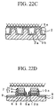
FIG. 22A is a fragmentary plane view illustrative of a semiconductor memory device having a trench isolation structure in a sixth step involved in a novel fabrication method in a third embodiment in accordance with the present invention.
FIG. 22B is a fragmentary cross sectional elevation view illustrative of a semiconductor memory device having a trench isolation structure in a sixth step involved in a novel fabrication method, taken along an IV—IV line of FIG. 22A.
FIG. 22C is a fragmentary cross sectional elevation view illustrative of a semiconductor memory device having a trench isolation structure in a sixth step involved in a novel fabrication method, taken along a V—V line of FIG. 22A.
FIG. 22D is a fragmentary cross sectional elevation view illustrative of a semiconductor memory device having a trench isolation structure in a sixth step involved in a novel fabrication method, taken along an VI—VI line of FIG. 22A.
DISCLOSURE OF THE INVENTION
The present invention provides a method of introducing an impurity into side walls of a trench groove formed in a substrate by carrying out an ion-implantation in an oblique direction with a rotation of the substrate.
The present invention also provides a method of introducing an impurity into side walls of trench grooves formed in a substrate, and the trench grooves being separated by ridged portions of the substrate so that the trench grooves and the ridged portions are aligned between adjacent two of gate electrode structures, wherein the method comprises the step of carrying out an ion-implantation in an oblique direction with a rotation of the substrate by use of the gate electrode structures as masks.
It is preferable that the gate electrode structures have side wall insulation films.
It is further preferable that the side wall insulation films on opposite side walls of each of the gate electrode structures have the same height.
It is also preferable that the side wall insulation films on opposite side walls of each of the gate electrode structures have different heights from each other.
It is also preferable that the gate electrode structure has a floating gate electrode and a control gate electrode.
The present invention provides a method of forming a diffusion layer which extends on bottoms and side walls of trench grooves as well as on top portions of ridged portions separating the trench grooves, and the trench grooves being separated by ridged portions of the substrate so that the trench grooves and the ridged portions are aligned between adjacent two of gate electrode structures, the method comprising the steps of: carrying out a first ion-implantation in a vertical direction to introduce an impurity into the bottoms of the trench grooves and into top portions of the ridged portions by use of gate electrode structures; forming side wall insulation films on side walls of the gate electrode structures; and carrying out a second ion-implantation in an oblique direction with a rotation of the substrate by use of the gate electrode structures and the side walls.
It is preferable that the side wall insulation films on opposite side walls of each of the gate electrode structures have the same height.
It is also preferable that the side wall insulation films on opposite side walls of each of the gate electrode structures have different heights from each other.
It is also preferable that the gate electrode structure has a floating gate electrode and a control gate electrode.
Preferred Embodiment
First Embodiment
A first embodiment according to the present invention will be described in detail with reference to the drawings. A novel method of forming a semiconductor memory device is provided.
FIG. 6A is a fragmentary plane view illustrative of a semiconductor memory device having a trench isolation structure in a first step involved in a novel fabrication method in a first embodiment in accordance with the present invention. FIG. 6B is a fragmentary cross sectional elevation view illustrative of a semiconductor memory device having a trench isolation structure in a first step involved in a novel fabrication method, taken along an IV—IV line of FIG. 6A. FIG. 6C is a fragmentary cross sectional elevation view illustrative of a semiconductor memory device having a trench isolation structure in a first step involved in a novel fabrication method, taken along a V—V line of FIG. 6A. FIG. 6D is a fragmentary cross sectional elevation view illustrative of a semiconductor memory device having a trench isolation structure in a first step involved in a novel fabrication method, taken along an VI—VI line of FIG. 6A.
The semiconductor memory device in this embodiment is a trench isolation NOR fresh memory cell, wherein each contact of bit line layer has two bits.
With reference to FIGS. 6A, 6B, 6C and 6D, a reactive ion etching is used to form trench grooves in a surface region of a semiconductor substrate 1 thereby to define a plurality of diffusion layers 2 in the semiconductor substrate 1, wherein each of the trench grooves have a stripe shape in plane view and a trench shape in sectional view. The trench grooves extend in a first horizontal direction and in parallel to each other at a constant pitch. The trench grooves are filled with silicon oxide to form a plurality of trench isolations 3 in the trench grooves, wherein each of the diffusion layers 2 are defined between the adjacent two of the trench isolations 3. The trench isolations 3 have a stripe shape in plane view and a trench shape in sectional view. The trench isolations 3 extend in a first horizontal direction and in parallel to each other at a constant pitch.
FIG. 7A is a fragmentary plane view illustrative of a semiconductor memory device having a trench isolation structure in a second step involved in a novel fabrication method in a first embodiment in accordance with the present invention. FIG. 7B is a fragmentary cross sectional elevation view illustrative of a semiconductor memory device having a trench isolation structure in a second step involved in a novel fabrication method, taken along an IV—IV line of FIG. 7A. FIG. 7C is a fragmentary cross sectional elevation view illustrative of a semiconductor memory device having a trench isolation structure in a second step involved in a novel fabrication method, taken along a V—V line of FIG. 7A. FIG. 7D is a fragmentary cross sectional elevation view illustrative of a semiconductor memory device having a trench isolation structure in a second step involved in a novel fabrication method, taken along an VI—VI line of FIG. 7A.
A gate insulation film is formed over surfaces of the diffusion layers 2. A floating gate electrode layer 5 is then formed on the gate insulation film. Laminations of the gate insulation film and the floating gate electrode layer are patterned to form gate insulation films 4 which cover the diffusion layers 2 and the floating gate electrodes 5 on the gate insulation films 4. The floating gate electrodes 5 extend in the first horizontal direction and in parallel to each other at the constant pitch.
FIG. 8A is a fragmentary plane view illustrative of a semiconductor memory device having a trench isolation structure in a third step involved in a novel fabrication method in a first embodiment in accordance with the present invention. FIG. 8B is a fragmentary cross sectional elevation view illustrative of a semiconductor memory device having a trench isolation structure in a third step involved in a novel fabrication method, taken along an IV—IV line of FIG. 8A. FIG. 8C is a fragmentary cross sectional elevation view illustrative of a semiconductor memory device having a trench isolation structure in a third step involved in a novel fabrication method, taken along a V—V line of FIG. 8A FIG. 8D is a fragmentary cross sectional elevation view illustrative of a semiconductor memory device having a trench isolation structure in a third step involved in a novel fabrication method, taken along an VI—VI line of FIG. 8A.
An inter-layer insulator 6 is formed over the substrate 1, so that the inter-layer insulator 6 covers the floating gate electrodes 5, wherein the inter-layer insulator 6 comprises laminations of a silicon oxide film, a silicon nitride film and a silicon oxide film. Control gate electrodes 7 are formed over the substrate 1 so that the control gate electrodes 7 are stripe shaped and extend in a second direction perpendicular to the first direction along which the trench isolations 3 extend. The control gate electrodes 7 comprises laminations of a polysilicon layer 7 a and a tungsten silicide layer 7 b on the polysilicon layer 7 a.
FIG. 9A is a fragmentary plane view illustrative of a semiconductor memory device having a trench isolation structure in a fourth step involved in a novel fabrication method in a first embodiment in accordance with the present invention. FIG. 9B is a fragmentary cross sectional elevation view illustrative of a semiconductor memory device having a trench isolation structure in a fourth step involved in a novel fabrication method, taken along an IV—IV line of FIG. 9A. FIG. 9C is a fragmentary cross sectional elevation view illustrative of a semiconductor memory device having a trench isolation structure in a fourth step involved in a novel fabrication method, taken along a V—V line of FIG. 9A. FIG. 9D is a fragmentary cross sectional elevation view illustrative of a semiconductor memory device having a trench isolation structure in a fourth step involved in a novel fabrication method, taken along an VI—VI line of FIG. 9A.
A photo-resist pattern 8 is selectively formed which has an opening which is positioned over a gap between the adjacent two of the control gate electrode 7 and also over confronting half sides of the adjacent two of the control gate electrode 7. The photo-resist pattern 8 and the control gate electrodes 7 are used as masks to carry out an etching to the trench isolations 3, so that trench grooves are formed.
FIG. 10A is a fragmentary plane view illustrative of a semiconductor memory device having a trench isolation structure in a fifth step involved in a novel fabrication method in a first embodiment in accordance with the present invention. FIG. 10B is a fragmentary cross sectional elevation view illustrative of a semiconductor memory device having a trench isolation structure in a fifth step involved in a novel fabrication method, taken along an IV—IV line of FIG. 10A. FIG. 10C is a fragmentary cross sectional elevation view illustrative of a semiconductor memory device having a trench isolation structure in a fifth step involved in a novel fabrication method, taken along a V—V line of FIG. 10A. FIG. 10D is a fragmentary cross sectional elevation view illustrative of a semiconductor memory device having a trench isolation structure in a fifth step involved in a novel fabrication method, taken along an VI—VI line of FIG. 10A.
An ion-implantation of an impurity such as arsenic is carried out by using the control gate electrodes 7 and the photo-resist pattern 8 as masks in a vertical direction to the surface of the substrate to form source diffusion layers 9 a in upper regions of the diffusion regions 2 and in bottom regions of the etched trench grooves 3 b. Etched trench grooves 3 b have a trench structure, for which reason an insufficient amount of an impurity such as arsenic is introduced to the side surfaces 2 a of the etched trench grooves 3 a. After the photoresist pattern 8 is removed, the control gate electrode 7 is used to carry out a second ion-implantation of an impurity such as arsenic to form source and drain diffusion layers 9. A silicon oxide film is grown on an entire surface of the substrate 1 for subsequent etch back to the silicon oxide film so as to form side wall oxide films 10 on both side walls of the control gate electrodes 7.
FIG. 11A is a fragmentary plane view illustrative of a semiconductor memory device having a trench isolation structure in a sixth step involved in a novel fabrication method in a first embodiment in accordance with the present invention. FIG. 11B is a fragmentary cross sectional elevation view illustrative of a semiconductor memory device having a trench isolation structure in a sixth step involved in a novel fabrication method, taken along an IV—IV line of FIG. 11A. FIG. 11C is a fragmentary cross sectional elevation view illustrative of a semiconductor memory device having a trench isolation structure in a sixth step involved in a novel fabrication method, taken along a V—V line of FIG. 11A. FIG. 11D is a fragmentary cross sectional elevation view illustrative of a semiconductor memory device having a trench isolation structure in a sixth step involved in a novel fabrication method, taken along an VI—VI line of FIG. 11A.
A third ion-implantation of an impurity such as arsenic is carried out in an oblique direction with rotation of the substrate 1 by use of the control gate electrodes 7 and the side wall oxide films 10 so as to introduce a sufficient amount of the impurity into the side surfaces of the etched trench grooves 3 a whereby the source diffusion layer 9 a is formed in the side surfaces 3 b of the etched trench grooves. The side wall oxide films 10 prevent introduction of the impurity into a channel region between the source and drain diffusion layers 9. As a result, a problem with a punch through can be prevented.
An isolation layer not illustrated is formed entirely over the substrate 1 for subsequent patterning the isolation layer to form a contact portion in the source and drain regions 9 whereby one section has one set of two floating gate electrodes 5 which sandwich the source diffusion layer 9 a. A bit line layer is formed so that the contact portion is filled with the bit line layer whereby the trench isolation NOR flash memory cell is formed, where one contact of the bit line layer has two bits.
In accordance with the above novel method, after the trench isolations were removed to have formed the etched trench grooves 3 a, then the ion-implantation is carried out in the oblique direction with rotation of the substrate so that the sufficient amount of the impurity can be introduced into the side surfaces 3 b of the etched trench grooves 3 a, thereby forming the diffusion layers can be formed on the side surfaces 3 b of the etched trench grooves 3 a. As a result, the resistance of the source diffusion layer 9 a can be reduced. The side wall oxide films 10 prevent introduction of the impurity into a channel region between the source and drain diffusion layers 9. As a result, a problem with a punch through can be prevented.
Second Embodiment
A second embodiment according to the present invention will be described in detail with reference to the drawings. A novel method of forming a semiconductor memory device is provided.
FIG. 12A is a fragmentary plane view illustrative of a semiconductor memory device having a trench isolation structure in a first step involved in a novel fabrication method in a second embodiment in accordance with the present invention. FIG. 12B is a fragmentary cross sectional elevation view illustrative of a semiconductor memory device having a trench isolation structure in a first step involved in a novel fabrication method, taken along an IV—IV line of FIG. 12A. FIG. 12C is a fragmentary cross sectional elevation view illustrative of a semiconductor memory device having a trench isolation structure in a first step involved in a novel fabrication method, taken along a V—V line of FIG. 12A. FIG. 12D is a fragmentary cross sectional elevation view illustrative of a semiconductor memory device having a trench isolation structure in a first step involved in a novel fabrication method, taken along an VI—VI line of FIG. 12A.
The semiconductor memory device in this embodiment is a trench isolation NOR fresh memory cell, wherein each contact of bit line layer has two bits.
With reference to FIGS. 12A, 12B, 12C and 12D, a reactive ion etching is used to form trench grooves in a surface region of a semiconductor substrate 1 thereby to define a plurality of diffusion layers 2 in the semiconductor substrate 1, wherein each of the trench grooves have a stripe shape in plane view and a trench shape in sectional view. The trench grooves extend in a first horizontal direction and in parallel to each other at a constant pitch. The trench grooves are filled with silicon oxide to form a plurality of trench isolations 3 in the trench grooves, wherein each of the diffusion layers 2 are defined between the adjacent two of the trench isolations 3. The trench isolations 3 have a stripe shape in plane view and a trench shape in sectional view. The trench isolations 3 extend in a first horizontal direction and in parallel to each other at a constant pitch.
FIG. 13A is a fragmentary plane view illustrative of a semiconductor memory device having a trench isolation structure in a second step involved in a novel fabrication method in a second embodiment in accordance with the present invention. FIG. 13B is a fragmentary cross sectional elevation view illustrative of a semiconductor memory device having a trench isolation structure in a second step involved in a novel fabrication method, taken along an IV—IV line of FIG. 13A. FIG. 13C is a fragmentary cross sectional elevation view illustrative of a semiconductor memory device having a trench isolation structure in a second step involved in a novel fabrication method, taken along a V—V line of FIG. 13A. FIG. 13D is a fragmentary cross sectional elevation view illustrative of a semiconductor memory device having a trench isolation structure in a second step involved in a novel fabrication method, taken along an VI—VI line of FIG. 13A.
A gate insulation film is formed over surfaces of the diffusion layers 2. A floating gate electrode layer 5 is then formed on the gate insulation film. Laminations of the gate insulation film and the floating gate electrode layer are patterned to form gate insulation films 4 which cover the diffusion layers 2 and the floating gate electrodes 5 on the gate insulation films 4. The floating gate electrodes 5 extend in the first horizontal direction and in parallel to each other at the constant pitch.
FIG. 14A is a fragmentary plane view illustrative of a semiconductor memory device having a trench isolation structure in a third step involved in a novel fabrication method in a second embodiment in accordance with the present invention. FIG. 14B is a fragmentary cross sectional elevation view illustrative of a semiconductor memory device having a trench isolation structure in a third step involved in a novel fabrication method, taken along an IV—IV line of FIG. 14A. FIG. 14C is a fragmentary cross sectional elevation view illustrative of a semiconductor memory device having a trench isolation structure in a third step involved in a novel fabrication method, taken along a V—V line of FIG. 14A. FIG. 14D is a fragmentary cross sectional elevation view illustrative of a semiconductor memory device having a trench isolation structure in a third step involved in a novel fabrication method, taken along an VI—VI line of FIG. 14A.
An inter-layer insulator 6 is formed over the substrate 1, so that the inter-layer insulator 6 covers the floating gate electrodes 5, wherein the inter-layer insulator 6 comprises laminations of a silicon oxide film, a silicon nitride film and a silicon oxide film. Control gate electrodes 7 are formed over the substrate 1 so that the control gate electrodes 7 are stripe shaped and extend in a second direction perpendicular to the first direction along which the trench isolations 3 extend. The control gate electrodes 7 comprises laminations of a polysilicon layer 7 a and a tungsten silicide layer 7 b on the polysilicon layer 7 a.
FIG. 15A is a fragmentary plane view illustrative of a semiconductor memory device having a trench isolation structure in a fourth step involved in a novel fabrication method in a second embodiment in accordance with the present invention. FIG. 15B is a fragmentary cross sectional elevation view illustrative of a semiconductor memory device having a trench isolation structure in a fourth step involved in a novel fabrication method, taken along an IV—IV line of FIG. 15A. FIG. 15C is a fragmentary cross sectional elevation view illustrative of a semiconductor memory device having a trench isolation structure in a fourth step involved in a novel fabrication method, taken along a V—V line of FIG. 15A. FIG. 15D is a fragmentary cross sectional elevation view illustrative of a semiconductor memory device having a trench isolation structure in a fourth step involved in a novel fabrication method, taken along an VI—VI line of FIG. 15A.
An ion-implantation of an impurity such as arsenic is carried out by using the control gate electrodes 7 as a mask in a vertical direction to the surface of the substrate to form source and drain diffusion layers 9. A silicon oxide film or a silicon nitride film is grown on an entire surface of the substrate 1 for subsequent etch back to the silicon oxide film so as to form side wall insulation films 10 on both side walls of the control gate electrodes 7.
FIG. 16A is a fragmentary plane view illustrative of a semiconductor memory device having a trench isolation structure in a fifth step involved in a novel fabrication method in a second embodiment in accordance with the present invention. FIG. 16B is a fragmentary cross sectional elevation view illustrative of a semiconductor memory device having a trench isolation structure in a fifth step involved in a novel fabrication method, taken along an IV—IV line of FIG. 16A. FIG. 16C is a fragmentary cross sectional elevation view illustrative of a semiconductor memory device having a trench isolation structure in a fifth step involved in a novel fabrication method, taken along a V—V line of FIG. 16A. FIG. 16D is a fragmentary cross sectional elevation view illustrative of a semiconductor memory device having a trench isolation structure in a fifth step involved in a novel fabrication method, taken along an VI—VI line of FIG. 16A.
A photo-resist pattern 8 is selectively formed which has an opening which is positioned over a gap between the adjacent two of the control gate electrode 7 and also over confronting half sides of the adjacent two of the control gate electrode 7. The trench isolations 3 are selectively etched by use of the photo-resist pattern 8 to form etched trench grooves 3 a. The used photo-resist pattern 8 is removed. An ion-implantation of an impurity such as arsenic is carried out by use of the control gate electrodes 7, the side wall insulation films 10 as masks in an oblique direction with rotation of the substrate 1 so as to introduce a sufficient amount of the impurity into the side surfaces 3 b of the etched trench grooves 3 a whereby the source diffusion layer 9 a is formed in the side surfaces 3 b of the etched trench grooves 3 a. The side wall oxide films 10 prevent introduction of the impurity into a channel region between the source and drain diffusion layers 9. As a result, a problem with a punch through can be prevented.
An isolation layer not illustrated is formed entirely over the substrate 1 for subsequent patterning the isolation layer to form a contact portion in the source and drain regions 9 whereby one section has one set of two floating gate electrodes 5 which sandwich the source diffusion layer 9 a. A bit line layer is formed so that the contact portion is filled with the bit line layer whereby the trench isolation NOR flash memory cell is formed, where one contact of the bit line layer has two bits.
In accordance with the above novel method, after the trench isolations were removed to have formed the etched trench grooves 3 a, then the ion-implantation is carried out in the oblique direction with rotation of the substrate so that the sufficient amount of the impurity can be introduced into the side surfaces 3 b of the etched trench grooves 3 a, thereby forming the diffusion layers can be formed on the side surfaces 3 b of the etched trench grooves 3 a. As a result, the resistance of the source diffusion layer 9 a can be reduced. The side wall oxide films 10 prevent introduction of the impurity into a channel region between the source and drain diffusion layers 9. As a result, a problem with a punch through can be prevented.
As compared to the first embodiment, this novel method has a reduced number of the fabrication processes.
Third Embodiment
A third embodiment according to the present invention will be described in detail with reference to the drawings. A novel method of forming a semiconductor memory device is provided.
FIG. 17A is a fragmentary plane view illustrative of a semiconductor memory device having a trench isolation structure in a first step involved in a novel fabrication method in a third embodiment in accordance with the present invention. FIG. 17B is a fragmentary cross sectional elevation view illustrative of a semiconductor memory device having a trench isolation structure in a first step involved in a novel fabrication method, taken along an IV—IV line of FIG. 17A. FIG. 17C is a fragmentary cross sectional elevation view illustrative of a semiconductor memory device having a trench isolation structure in a first step involved in a novel fabrication method, taken along a V—V line of FIG. 17A. FIG. 17D is a fragmentary cross sectional elevation view illustrative of a semiconductor memory device having a trench isolation structure in a first step involved in a novel fabrication method, taken along an VI—VI line of FIG. 17A.
The semiconductor memory device in this embodiment is a trench isolation NOR fresh memory cell, wherein each contact of bit line layer has two bits.
With reference to FIGS. 17A, 17B, 17C and 17D, a reactive ion etching is used to form trench grooves in a surface region of a semiconductor substrate 1 thereby to define a plurality of diffusion layers 2 in the semiconductor substrate 1, wherein each of the trench grooves have a stripe shape in plane view and a trench shape in sectional view. The trench grooves extend in a first horizontal direction and in parallel to each other at a constant pitch. The trench grooves are filled with silicon oxide to form a plurality of trench isolations 3 in the trench grooves, wherein each of the diffusion layers 2 are defined between the adjacent two of the trench isolations 3. The trench isolations 3 have a stripe shape in plane view and a trench shape in sectional view. The trench isolations 3 extend in a first horizontal direction and in parallel to each other at a constant pitch.
FIG. 18A is a fragmentary plane view illustrative of a semiconductor memory device having a trench isolation structure in a second step involved in a novel fabrication method in a third embodiment in accordance with the present invention. FIG. 18B is a fragmentary cross sectional elevation view illustrative of a semiconductor memory device having a trench isolation structure in a second step involved in a novel fabrication method, taken along an IV—IV line of FIG. 18A. FIG. 18C is a fragmentary cross sectional elevation view illustrative of a semiconductor memory device having a trench isolation structure in a second step involved in a novel fabrication method, taken along a V—V line of FIG. 18A. FIG. 18D is a fragmentary cross sectional elevation view illustrative of a semiconductor memory device having a trench isolation structure in a second step involved in a novel fabrication method, taken along an VI—VI line of FIG. 18A.
A gate insulation film is formed over surfaces of the diffusion layers 2. A floating gate electrode layer 5 is then formed on the gate insulation film. Laminations of the gate insulation film and the floating gate electrode layer are patterned to form gate insulation films 4 which cover the diffusion layers 2 and the floating gate electrodes 5 on the gate insulation films 4. The floating gate electrodes 5 extend in the first horizontal direction and in parallel to each other at the constant pitch.
FIG. 19A is a fragmentary plane view illustrative of a semiconductor memory device having a trench isolation structure in a third step involved in a novel fabrication method in a third embodiment in accordance with the present invention. FIG. 19B is a fragmentary cross sectional elevation view illustrative of a semiconductor memory device having a trench isolation structure in a third step involved in a novel fabrication method, taken along an IV—IV line of FIG. 19A. FIG. 19C is a fragmentary cross sectional elevation view illustrative of a semiconductor memory device having a trench isolation structure in a third step involved in a novel fabrication method, taken along a V—V line of FIG. 19A. FIG. 19D is a fragmentary cross sectional elevation view illustrative of a semiconductor memory device having a trench isolation structure in a third step involved in a novel fabrication method, taken along an VI—VI line of FIG. 19A.
An inter-layer insulator 6 is formed over the substrate 1, so that the inter-layer insulator 6 covers the floating gate electrodes 5, wherein the inter-layer insulator 6 comprises laminations of a silicon oxide film, a silicon nitride film and a silicon oxide film. Control gate electrodes 7 are formed over the substrate 1 so that the control gate electrodes 7 are stripe shaped and extend in a second direction perpendicular to the first direction along which the trench isolations 3 extend. The control gate electrodes 7 comprises laminations of a polysilicon layer 7 a and a tungsten silicide layer 7 b on the polysilicon layer 7 a.
FIG. 20A is a fragmentary plane view illustrative of a semiconductor memory device having a trench isolation structure in a fourth step involved in a novel fabrication method in a third embodiment in accordance with the present invention. FIG. 20B is a fragmentary cross sectional elevation view illustrative of a semiconductor memory device having a trench isolation structure in a fourth step involved in a novel fabrication method, taken along an IV—IV line of FIG. 20A. FIG. 20C is a fragmentary cross sectional elevation view illustrative of a semiconductor memory device having a trench isolation structure in a fourth step involved in a novel fabrication method, taken along a V—V line of FIG. 20A. FIG. 20D is a fragmentary cross sectional elevation view illustrative of a semiconductor memory device having a trench isolation structure in a fourth step involved in a novel fabrication method, taken along an VI—VI line of FIG. 20A.
An ion-implantation of an impurity such as arsenic is carried out by using the control gate electrodes 7 as a mask in a vertical direction to the surface of the substrate to form source and drain diffusion layers 9. A silicon oxide film or a silicon nitride film is grown on an entire surface of the substrate 1 for subsequent etch back to the silicon oxide film so as to form first side wall insulation film 10 b on a first side wall of the control gate electrodes 7 in side of the source diffusion layer 9 a and second side wall insulation film 10 c on a second side wall opposite to the first side wall, wherein the height of the first side wall insulation film 10 b is higher than the height of the second side wall insulation film 10 c.
FIG. 21A is a fragmentary plane view illustrative of a semiconductor memory device having a trench isolation structure in a fifth step involved in a novel fabrication method in a third embodiment in accordance with the present invention. FIG. 21B is a fragmentary cross sectional elevation view illustrative of a semiconductor memory device having a trench isolation structure in a fifth step involved in a novel fabrication method, taken along an IV—IV line of FIG. 21A. FIG. 21C is a fragmentary cross sectional elevation view illustrative of a semiconductor memory device having a trench isolation structure in a fifth step involved in a novel fabrication method, taken along a V—V line of FIG. 21A. FIG. 21D is a fragmentary cross sectional elevation view illustrative of a semiconductor memory device having a trench isolation structure in a fifth step involved in a novel fabrication method, taken along an VI—VI line of FIG. 21A.
A photo-resist pattern 8 is selectively formed which has an opening which is positioned over a gap between the adjacent two of the control gate electrode 7 and also over confronting half sides of the adjacent two of the control gate electrode 7. The trench isolations 3 are selectively etched by use of the photo-resist pattern 8 to form etched trench grooves 3 a. The used photo-resist pattern 8 is removed.
FIG. 22A is a fragmentary plane view illustrative of a semiconductor memory device having a trench isolation structure in a sixth step involved in a novel fabrication method in a third embodiment in accordance with the present invention. FIG. 22B is a fragmentary cross sectional elevation view illustrative of a semiconductor memory device having a trench isolation structure in a sixth step involved in a novel fabrication method, taken along an IV—IV line of FIG. 22A. FIG. 22C is a fragmentary cross sectional elevation view illustrative of a semiconductor memory device having a trench isolation structure in a sixth step involved in a novel fabrication method, taken along a V—V line of FIG. 22A. FIG. 22D is a fragmentary cross sectional elevation view illustrative of a semiconductor memory device having a trench isolation structure in a sixth step involved in a novel fabrication method, taken along an VI—VI line of FIG. 22A.
An ion-implantation of an impurity such as arsenic is carried out by use of the control gate electrodes 7, the first and second side wall insulation films 10 b and 10 c as masks in an oblique direction with rotation of the substrate 1 so as to introduce a sufficient amount of the impurity into the side surfaces 3 b of the etched trench grooves 3 a whereby the source diffusion layer 9 a is formed in the side surfaces 3 b of the etched trench grooves 3 a. The first and second side wall oxide films 10 b and 10 c prevent introduction of the impurity into a channel region between the source and drain diffusion layers 9. As a result, a problem with a punch through can be prevented. The height of the second side wall oxide film 10 c is lower than the height of the first side wall oxide film 10 b, so that it is more easy to introduce the impurity into the source diffusion layers 9 a as compared to when the first and second side wall oxide films have the same height as each other.
An isolation layer not illustrated is formed entirely over the substrate 1 for subsequent patterning the isolation layer to form a contact portion in the source and drain regions 9 whereby one section has one set of two floating gate electrodes 5 which sandwich the source diffusion layer 9 a. A bit line layer is formed so that the contact portion is filled with the bit line layer whereby the trench isolation NOR flash memory cell is formed, where one contact of the bit line layer has two bits.
In accordance with the above novel method, after the trench isolations were removed to have formed the etched trench grooves 3 a, then the ion-implantation is carried out in the oblique direction with rotation of the substrate so that the sufficient amount of the impurity can be introduced into the side surfaces 3 b of the etched trench grooves 3 a, thereby forming the diffusion layers can be formed on the side surfaces 3 b of the etched trench grooves 3 a. As a result, the resistance of the source diffusion layer 9 a can be reduced. The side wall oxide films 10 prevent introduction of the impurity into a channel region between the source and drain diffusion layers 9. As a result, a problem with a punch through can be prevented.
Whereas modifications of the present invention will be apparent to a person having ordinary skill in the art, to which the invention pertains, it is to be understood that embodiments as shown and described by way of illustrations are by no means intended to be considered in a limiting sense. Accordingly, it is to be intended to cover by claims all modifications which fall within the spirit and scope of the present invention.