US6417848B1 - Pixel clustering for improved graphics throughput - Google Patents
Pixel clustering for improved graphics throughput Download PDFInfo
- Publication number
- US6417848B1 US6417848B1 US08/918,276 US91827697A US6417848B1 US 6417848 B1 US6417848 B1 US 6417848B1 US 91827697 A US91827697 A US 91827697A US 6417848 B1 US6417848 B1 US 6417848B1
- Authority
- US
- United States
- Prior art keywords
- cluster
- current
- pixels
- pixel
- clusterizer
- Prior art date
- Legal status (The legal status is an assumption and is not a legal conclusion. Google has not performed a legal analysis and makes no representation as to the accuracy of the status listed.)
- Expired - Lifetime
Links
- 230000015654 memory Effects 0.000 claims abstract description 183
- 238000012545 processing Methods 0.000 claims abstract description 48
- 238000002156 mixing Methods 0.000 claims abstract description 16
- 239000000945 filler Substances 0.000 claims abstract description 9
- 239000000872 buffer Substances 0.000 claims description 41
- 238000000034 method Methods 0.000 claims description 36
- 238000012546 transfer Methods 0.000 description 10
- 230000009471 action Effects 0.000 description 9
- 230000002093 peripheral effect Effects 0.000 description 7
- 230000008569 process Effects 0.000 description 6
- 238000010586 diagram Methods 0.000 description 5
- 230000006870 function Effects 0.000 description 5
- 238000013507 mapping Methods 0.000 description 5
- 238000001514 detection method Methods 0.000 description 4
- 230000008901 benefit Effects 0.000 description 3
- 230000000694 effects Effects 0.000 description 3
- 238000012360 testing method Methods 0.000 description 3
- 238000006243 chemical reaction Methods 0.000 description 2
- 102100031456 Centriolin Human genes 0.000 description 1
- 101000941711 Homo sapiens Centriolin Proteins 0.000 description 1
- 238000013461 design Methods 0.000 description 1
- 238000009792 diffusion process Methods 0.000 description 1
- 230000009977 dual effect Effects 0.000 description 1
- 231100001261 hazardous Toxicity 0.000 description 1
- 230000003993 interaction Effects 0.000 description 1
- 239000000203 mixture Substances 0.000 description 1
- 230000005236 sound signal Effects 0.000 description 1
- 230000003068 static effect Effects 0.000 description 1
- 230000009466 transformation Effects 0.000 description 1
Images


Classifications
-
- G—PHYSICS
- G06—COMPUTING; CALCULATING OR COUNTING
- G06T—IMAGE DATA PROCESSING OR GENERATION, IN GENERAL
- G06T1/00—General purpose image data processing
- G06T1/20—Processor architectures; Processor configuration, e.g. pipelining
Definitions
- the present invention relates to computer-generated 3-D graphics.
- the present invention relates to the architecture of a media processor, which combines a programmable processor with dedicated hardware to process 3-D images represented by polygons.
- the surfaces of 3-D objects are approximated using polygons (typically triangles).
- polygons typically triangles.
- Using smaller polygons creates more realistic 3-D objects on the computer screens.
- using smaller polygons requires a larger number of polygons to represent an object.
- a polygon can be described by the polygon's vertices.
- the description of a vertex includes the coordinates of the vertex in object space, i.e. (x, y, z); perspective projection parameters (w, s, t); the color of the vertex, typically using color space coordinates (r, g, b); an alpha parameter; and a fog parameter.
- the vertex information is processed through well known setup processes into a parameter list suitable for a 3-D pipeline. The exact parameter list format depends on the 3-D pipeline used.
- the 3-D pipeline performs rasterization of the polygons, i.e. the conversion of polygons into pixels in object space.
- a common rasterization algorithm for polygons includes four major steps: walk edges, walk spans, texture pixels, and apply fog effects. Many elements of the theory and techniques of rasterization are known to those skilled in the art.
- Texturing pixels is a technique for mapping an image (“texture”) onto the polygonal surfaces of a computer-generated object, so as to allow the object to appear more realistic in a displayed scene.
- Texture mapping allows a texture to be superimposed onto each polygon of an object, using transformation techniques that compensate the appearance of the texture in each polygon for lighting conditions, angles of viewing and other conditions which may affect the appearance of the object.
- transformation techniques that compensate the appearance of the texture in each polygon for lighting conditions, angles of viewing and other conditions which may affect the appearance of the object.
- the object space pixels are blended in a blender or back end processor to create 2-D images suitable for graphic displays.
- the blender or back end processor performs Z-buffering and alpha blending on the object space pixels.
- Z-Buffering determines which object space pixels can be seen on the graphics screen. Specifically, Z-buffering compares the z coordinate each object space pixel against the z coordinate of the screen space pixel with the same x and y coordinates in the frame buffer. If the object space pixel is in front of the frame buffer pixel the parameters of the object space pixel is stored in the frame buffer otherwise the contents of the frame buffer remain unchanged.
- the frame buffer is typically addressed by mapping the x and y coordinates of a pixel into a memory address.
- the frame buffer stores parameters regarding the pixel such as color space values and the Z coordinate.
- Alpha blending controls the translucence of the conversion from object space to screen space.
- the screen space pixels are stored in a frame buffer for displaying on a graphics display. Many elements of the theory and techniques of Z-buffering and alpha blending are known to those skilled in the art.
- a 3-D image probably includes thousands of polygons for real-time application or even millions of polygons for high-resolution 3-D images.
- the setup procedure for these polygons can be performed on a programmable processor.
- many 3-D graphics systems use dedicated hardware for the setup procedure.
- Most 3-D graphics system uses dedicated hardware to perform rasterization. Rasterization generates about 50 pixels for small polygons used in detailed 3-D graphics and about 400 pixels for polygons in used for 3-D games. Therefore, a rasterization of a high quality 3-D image may generate over a million pixels in object space. Consequently, back end processors which perform Z-buffering and alpha blending are implemented using dedicated hardware which must be coupled to the frame buffer.
- Many 3-D graphic system combine the functions of the back end processor with the 3-D pipeline.
- 3-D image processing typically involves one or more fast processing units in conjunction with a dedicated 3-D pipeline and a large amount of memory for image data and intermediate results.
- setup, rasterization, and blending are both computational and memory intensive. Since many features of the 3-D pipeline and back end processor require complex computation, the 3-D pipelines and back end processors require many transistors to implement and consequently consume a large area on integrated circuits. Furthermore, direct hardware implementations of algorithms can not be easily changed to take advantage of new algorithms or new techniques. Hence, there is a need for architectures and methods which allow parts of the 3-D pipeline and blender to be implemented using programmable processors.
- the present invention provides a 3-D graphics system which provides high performance and flexibility.
- the 3-D graphics system includes a software programmed setup processor, a 3-D pipeline, and a software programmed back end processor.
- the software programmed setup processor performs “setup” on polygons.
- the 3-D pipeline rasterizes the polygons into pixels which undergo back end processing, such as Z-buffering and alpha blending, in the software programmed setup processor.
- back end processing such as Z-buffering and alpha blending
- the setup processor and the back end processor are implemented as SIMD vector processors.
- the setup processor and the back end processor are both programmed on one SIMD vector processor.
- some embodiments of the invention includes a clusterizer to eliminate potential hazards for the SIMD vector processor.
- the clusterizer combines pixels into clusters which have no potential hazards for the back end processor.
- the clusterizer also eliminates potential hazards between clusters which may be interleaved by the back end processor.
- the back end processor can process the clusters from the clusterizer without wasting processing cycles resolving data coherence issues.
- the clusterizer can create clusters in which all pixel in the cluster are on the same page of a memory to reduce memory access times and latencies.
- the clusterizer builds clusters one pixel at a time.
- the clusterizer checks for potential hazards between the current cluster and the current pixel as well as between the current pixel and previous clusters. If no potential hazard exists and the current pixel is on the same page of memory as the other pixels in the current cluster, the clusterizer adds the current pixel to the current cluster. Otherwise the clusterizer outputs the current cluster, possibly one or more null clusters, and starts a new cluster with the current pixel.
- clusters are fixed size. Therefore, if a potential hazard or problem prevents the current pixel from being placed in the current cluster, the current cluster must be outputted before it is full.
- some embodiments of the clusterizer includes a cluster filler which fills the cluster with addresses that do not cause potential hazards for the back end processor.
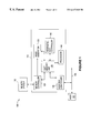
- FIG. 1 shows a computer system 100 to which one embodiment of the present invention is applicable.
- FIG. 2 shows a second embodiment of computer system to which one embodiment of the present invention is applicable.
- FIG. 3 shows a block diagram of a processor in accordance with one embodiment of the present invention for processing 3-D graphics.
- FIG. 4 shows a data flow diagram for processing 3-D graphics by one embodiment of the present invention.
- FIG. 5 shows a graphics display for use with embodiments of the present invention.
- FIG. 6 shows three pipelines for back end processing of clusters in accordance with one embodiment of the present invention.
- FIG. 7 shows a flow chart for a clusterizer in accordance with one embodiment of the present invention.
- FIG. 8 shows a cluster format for use with one embodiment of the present invention.
- FIG. 9 shows a detailed flow chart for a clusterizer in accordance with one embodiment of the present invention.
- FIGS. 10 ( a )- 10 ( d ) are circuits to create unique group addresses in accordance with one embodiment of the present invention.
- FIG. 11 is a block diagram of a clusterizer in accordance with one embodiment of the present invention.
- FIG. 1 shows a computer system 100 to which one embodiment of the present invention is applicable.
- a media processor 110 accesses a memory system 105 , which includes a frame buffer as well as program memory.
- Media processor 110 typically operates under control of a host 150 and interfaces with a number of multimedia peripherals.
- FIG. 1 shows media processor 110 includes (a) a video subsystem 125 for interfacing with various video and graphics displays (b) a peripheral bus controller 145 to interface peripherals implemented on media processor 110 such as modems and audio equipment to other systems, and (c) a host bus controller 135 to communicate with devices on host bus 155 , such as host 150 .
- Media processor 110 includes a processor 140 , which may include a 3-D pipeline and a programmable processing unit.
- a fast memory unit 106 is used as an instruction cache, a data cache and a texture cache for memory system 105 .
- a texture cache architecture suitable for media processor 110 is described in U.S. patent application Ser. No. 08/918,226 entitled “Reconfigureable Texture Cache,” naming James T. Battle as inventor, assigned to the assignee of this application and filed on even date herewith with Attorney Docket No. M-5120 US, which is hereby incorporated by reference in its entirety.
- FIG. 2 shows a media processor 110 B, which is a specific embodiment of media processor 110 , coupled to various peripheral components and video equipment.
- Media processor 110 B is implemented as a single chip.
- Memory system 105 includes two Rambus memory banks 205 a and 205 b .
- memory controller 120 To access Rambus memory banks 205 a and 205 b , memory controller 120 becomes a Rambus memory access control circuit 220 , which design is provided by Rambus, Inc. of Mountain View, Calif.
- Media processor 110 B uses a PCI bus 255 under control of PCI bus controller 235 , in place of generic host bus controller 135 .
- Video subsystem 125 is expanded to include (a) an on-chip video controller 211 providing an 8-bit digital video signal on video output bus 212 and receiving an 8-bit digital video signal on video input bus 213 , and (b) an on-chip RAMDAC unit 110 interfacing with a 16-bit graphics output bus, which drives an external graphics display terminal over graphics bus 222 .
- the 8-bit video signals of video input bus 213 and video output bus 212 are respectively encoded and decoded by NTSC/PAL encoder 215 and NTSC/PAL decoder 214 .
- FIG. 2 shows media processor 110 B interfacing through on-chip peripheral bus controller 145 to (a) a 3-terminal analog interface 216 and (b) an 8-bit peripheral interface 221 .
- a peripheral control unit 217 is coupled to analog bus 221 and analog interface 216 to provide multichannel audio signals, a modem, and other applications.
- Processor 140 includes a processor control unit 208 and a processor datapath 207 , which includes multi-stage pipelined arithmetic logic units.
- Fast memory unit 106 in media processor 110 B is a static random access memory (SRAM) unit 206 , which provides a total of 8K bytes of memory for use as an instruction cache, a data cache and a texture cache.
- SRAM static random access memory
- FIG. 3 provides a block diagram of one embodiment of processor 140 with fast memory unit 106 .
- processor 140 includes a programmable processing unit 310 , a 3-D pipeline 320 , and a clusterizer 340 .
- Programmable processing unit 310 , 3-D pipeline 320 , and clusterizer 340 are coupled to fast memory unit 106 .
- some embodiments of fast memory unit 106 are multiported so programmable processing unit 310 , 3-D pipeline 320 , and clusterizer 340 can access fast memory unit 106 simultaneously.
- programmable processing unit 310 is a vector signal processor (VSP) and includes multiple arithmetic logic units which work in parallel as a SIMD (Single instruction multiple data) processor.
- VSP vector signal processor
- 3-D pipeline 320 performs rasterization on polygons.
- 3-D pipeline 320 includes thirty stages to perform rasterization. The first three stages receive the polygons into 3-D pipeline 320 . The next three stages generate spans for the polygons. The next three stages generate pixels from the spans of the polygon. Ten stages are then used to apply perspective to the pixels. The next three stages generate texture addresses for a texture cache. Two more stages are used to access the texture cache and format texels from the texture cache. The next two stages apply various filters to the texels as needed. Then two stages blend and modulate the pixels and texels. Diffusion and specular lighting effects may also be applied. The final two stages apply fog effects to the pixels.
- Clusterizer 340 groups pixels into clusters to facilitate back end processing.
- Clusters are data structures that groups pixels in format ideal for vector SIMD operations.
- clusters can be customized to avoid some latencies of memory system 105 .
- clusters might be configured to only include pixels on the same “page” of memory in memory system 105 .
- a cluster format in accordance with one embodiment of the invention is described in detail below.
- clusterizer 340 is a five stage pipeline which is combined with 3-D pipeline 320 to form a 35 stage 3-D pipeline.
- FIG. 4 conceptually illustrates the interaction of fast memory unit 106 , programmable processing unit 310 , 3-D pipeline 320 , and clusterizer 340 .
- arrows denote data transfers rather than connection between devices.
- fast memory unit 106 is shown to be segmented by data types which does not necessarily reflect actual use of fast memory unit 106 .
- programmable processor 310 can be conceptually split into a software programmed setup processor 470 for performing setup and a software programmed back end processor 480 for performing Z-buffering and alpha blending.
- Host 150 provides polygon information in the form of raw vertex information to fast memory unit 106 at data transfer 425 .
- Programmable processing unit 310 reads the raw vertex information from fast memory unit 106 via data transfer 430 . After converting the raw vertex information to a parameter list suitable for 3-D pipeline 320 , programmable processing unit 310 writes the parameter list into fast memory unit 106 via data transfer 435 .
- 3-D pipeline 320 reads the parameter lists from fast memory unit 106 via data transfer 440 and rasterizes the parameter lists to generate raw pixels.
- the raw pixels are sent to clusterizer 340 via data transfer 445 .
- Clusterizer 340 forms clusters (as described below) from the raw pixels and stores the clusters in fast memory unit 106 via data transfer 450 .
- Programmable processing unit 310 retrieves the clusters from fast memory unit 106 via data transfer 455 .
- Programmable processing unit 310 also retrieves pixels from frame buffer 410 , which is part of memory system 105 , through fast memory unit 106 , which acts as a frame buffer cache, via data transfer 460 .
- programmable processing unit 310 After performing Z-buffering and alpha blending, programmable processing unit 310 writes pixel information back to frame buffer 106 through fast memory unit 106 via data transfer 465 .
- clusterizer 340 forms clusters of pixels which are suitable for rapid processing by programmable processing unit 310 . Pixels in a cluster share certain attributes including (a) the pixels can be retrieved from frame buffer 410 rapidly, (b) the pixels have the same control parameters for back end processing, and (c) the pixels do not cause coherency problems during Z-buffering or alpha blending.
- Clusterizer 340 can also be used with hardware implementations of Z-buffering and alpha blending.
- DRAMs dynamic random access memories
- fast DRAMs such as fast page mode DRAMs and Rambus DRAMs (RDRAMs)
- RDRAMs Rambus DRAMs
- the pixels from 3-D pipeline 320 still exhibit 2-D locality in display space.
- the 2-D locality can be attributed to the 2-D locality in the original polygons used to generate the pixels. Therefore, the pages of memory system 105 should be mapped into two dimensional “tile” in screen space to improve clusterization of the pixels.
- FIG. 5 shows a common mapping of memory pages to a rectangular graphics display screen 510 .
- Graphic display screen 510 is typically addressed with an x coordinate and a y coordinate in the form (x,y).
- the top left corner is typically assigned address (0,0) and the bottom right corner is assigned address (x max , y max ) Consequently, the top right corner is assigned address (x max , 0) and the bottom left corner is assigned address (0, y max ),
- a memory page of memory system 105 is mapped to each of the dotted rectangles tiles, such as tiles 520 , 530 , and 540 .
- every pixel in one of the tiles is in the same memory page of memory system 105 .
- every pixel in a cluster is also located in the same tile of display screen 510 .
- Other tile shapes such as triangles and hexagons may also be used.
- Memory addresses in memory system 105 can be in the form: base address+an offset.
- Memory addresses in frame buffer 410 can be defined by just the offset if the base address is assumed to be the start of the frame buffer in memory system 105 .
- the offset for frame buffer 410 can be split into a page address+a pixel/group offset.
- the page address corresponds to the address of the start of a page and the pixel/group address defines a pixel or group of pixels in the page.
- the page address of the memory page corresponding to tile 505 is equal to zero.
- page address increases left to right and top to bottom.
- the page address corresponding to tile 540 is greater than the page address corresponding to tile 517 which is greater than the page address of tile 515 which is greater than the page address corresponding to tile 505 .
- pixel/group addresses increase from left to right and top to bottom.
- the page address corresponding to tile 515 is 7*PS; the page address corresponding to tile 517 is 8*PS; and the page address corresponding to tile 540 is 47*PS.
- Equation (2) calculates the page address, PA, from a pixel address (x,y), where T sx is the number of tiles across a graphics display.
- PA PS * ⁇ int ⁇ ( x T x ) + T Sx * int ⁇ ( y T y ) ⁇ ( 2 )
- clusters store the page address, PA, of all the pixels in the cluster and the pixel/group addresses, PGO, of each pixel or group in the cluster.
- the pixel location of the pixel within the group, P loc is equal to x mod P dw .
- graphics frame buffer 410 For purely 2-D graphics frame buffer 410 only needs to store the color space information of a pixel. However, for 3-D graphics frame buffer 410 must store both the color space information of each pixel and the Z coordinate of each pixel. Typically frame buffer 410 stores the Z coordinates together in one section of memory and the color space information in another section of memory. Graphics display 510 is tiled with both a color space tile system and a z-coordinate tile system. Since the number of bits required for color space information may differ from the number of bits required for the Z coordinate, the size of pixel groups for color space may differ from the size of pixel groups for Z coordinates. Furthermore, the size of color space tiles may be different than the size of Z-coordinate tiles. The memory page address and pixel/group address for color space can be computed using equations (1), (2), and (3) using the appropriate size information for color space.
- clusterizer 340 must insure that a single cluster contains only pixels with the same control parameters.
- clusterizer 340 should create clusters which are free from processing hazards such as write-after-write hazards and read-before-write hazards. The specific types of hazards that must be avoided depend on the specific implementation of clusterizer 340 , and the implementation of the back end processing.
- a hazard which is common to almost all implementations of clusterizer 340 for SIMD versions of the Z-buffering algorithms is having two overlapping pixels in a cluster. Overlapping pixels in object space have the same x coordinates and the same y coordinates. Since a SIMD Z-buffering algorithm performs Z-buffering on both pixels simultaneously, an incorrect Z fb (x,y) and RGB fb (x, y) may result depending on which pixel is written into the frame buffer last.
- intercluster hazards may also occur.
- An intercluster hazard due to interleaved clusters is illustrated in FIG. 6 .
- back end processing are performed with pipeline 610 , pipeline 620 , and pipeline 630 .
- Pipelines 610 , 620 , and 630 may be actual physical pipelines in hardware back end processor are software constructs in software programmed back end processor 480 (FIG. 4 ).
- pipeline 610 reads cluster one information from fast memory unit 106 (see FIG. 4 ). Reading cluster information as used with respect to FIG. 6 includes reading the cluster pixels as well as reading the corresponding information in frame buffer 410 .
- pipeline 610 processes cluster one and pipeline 620 reads cluster two information from fast memory unit 106 .
- pipeline 610 finally stores cluster one information; pipeline 620 processes cluster two, and pipeline 630 reads cluster three information.
- Storing cluster information as used with respect to FIG. 6 refers to storing the frame buffer pixel information associated with the cluster.
- clusterizer 340 To avoid these hazards clusterizer 340 must insure that no overlapping pixels are in consecutive clusters and overlapping pixels are not in clusters separated by only one cluster. A technique to avoid intercluster hazards using null clusters is explained in detail below.
- Null clusters contain no valid data and can be processed very quickly during back end processing. For example, (see FIG. 6) if the current pixel overlaps with a pixel in Cluster one, clusterizer 630 make cluster two and cluster three into null clusters and place the current pixel into cluster four which has no hazard with cluster one, because cluster one information is stored before cluster four information is read.
- clusterizer 340 the structure of a cluster, the granularity of memory system 105 , or the granularity of fast memory unit 106 may cause an additional hazard, which should be avoided. Specifically, if the granularity of memory system 105 is a group of pixels, i.e.
- a common cause of group access occurs if a single data word of frame buffer 410 can contain several pixels. For example if a data word in frame buffer 410 is 72 bits wide and a pixel only requires 18 bits to store the Z coordinate of the pixel, a single access to frame buffer 410 can read or write four pixels worth of information.
- An intercluster group hazard can occur if cluster one contains a first pixel in group one, cluster two contains a second pixel in group one, and all accesses to frame buffer 410 results in reading or writing all of the pixels in a group. If cluster two information is read before cluster one information is stored, a read before write hazard occurs if the first pixel of group one was to be modified.
- FIG. 7 summarizes the major functions of clusterizer 340 in a flowchart 700 .
- Clusterizer 340 receives the current pixel from 3-D pipeline 320 in RECEIVE PIXEL 710 .
- Clusterizer 340 converts the current pixel to a format compatible with the cluster format in CONVERT PIXEL FORMAT 720 .
- Cluster formats can vary. A specific cluster format is described below in detail.
- clusterizer 340 converts the x and y coordinate of the pixel into a page addresses and a pixel/group address in CONVERT PIXEL FORMAT 720 .
- clusterizer 340 must test for potential hazards, in TEST FOR HAZARDS 730 . If no potential hazards are detected and the current cluster is not full, clusterizer 340 adds the pixel to the current cluster in ADD PIXEL 740 . Clusterizer 340 then waits for another pixel in RECEIVE PIXEL 710 .
- the current pixel may have potential hazards with the current cluster as well as with one or more previous clusters. For example, for three level of interleaving, as in FIG. 6, the current pixel may have potential hazards with the current cluster, the first previous cluster, and the second previous cluster, i.e. the cluster immediately before the previous cluster. Assuming the back end processor uses P ipe pipelines, than clusterizer 340 must detect potential hazards with the current cluster and the previous P ipe - 1 clusters.
- clusterizer 340 stores the current cluster for future hazard detection in STORE CLUSTER 770 .
- the current cluster is also written out of clusterizer 340 in WRITE CLUSTER 780 .
- a new cluster containing the current pixel is created in START NEW CLUSTER 790 .
- the new cluster becomes the current cluster and clusterizer 340 then waits for another pixel in RECEIVE PIXEL 710 .
- clusterizer 340 stores the current cluster for future hazard detection in STORE CLUSTER 770 .
- the current cluster is also written out of clusterizer 340 in WRITE CLUSTER 780 .
- Clusterizer 340 then inserts null clusters to space out the current pixel from the hazard causing previous cluster.
- clusterizer 340 if a potential hazard exists with the current cluster, clusterizer 340 must write and store P ipe - 1 null clusters in WRITE and STORE NULL CLUSTERS 764 .
- the recent previous clusters up to the ERP cluster are numbered from 1 to P ipe - 1 .
- clusterizer 340 must write and store P ipe - 1 -PC h null clusters in WRITE AND STORE NULL CLUSTERS 764 .
- clusterizer 340 After writing and storing the necessary number of null clusters, clusterizer 340 starts a new cluster containing the current pixel in START NEW CLUSTER 790 . The new cluster becomes the current cluster and clusterizer 340 then waits for another pixel in RECEIVE PIXEL 710 .
- clusterizer 340 stores the current cluster for future intercluster hazard detection in STORE CLUSTER 770 .
- the current cluster is also written out of clusterizer 340 in WRITE CLUSTER 780 .
- a new cluster containing the current pixel is created in START NEW CLUSTER 790 .
- the new cluster becomes the current cluster and clusterizer 340 then waits for another pixel in RECEIVE PIXEL 710 .
- FIG. 7 describes embodiments of clusterizer 340 in which only one cluster is created at a time. However, some embodiments of clusterizer 340 may try and build multiple clusters simultaneously. Using multiple clusters may lead to better utilization of the back end processor. However to benefit from better utilization of the back end processor, clusterizer 340 should provide clusters at a rate equal to or exceeding the rate that the back end processor can process clusters.
- FIG. 8 illustrates a specific cluster format 850 for use with media processor 110 B (FIG. 2 ), which uses Rambus DRAMs in memory system 105 .
- Each data word in cluster format 850 is 72 bits wide.
- the Z coordinate of a pixel is only 18 bits; therefore, each data word can contain a group of up to four pixels.
- the number of pixels per group may be limited by the size of the ARGB (Alpha, Red, Green Blue) information about a pixel.
- Common formats of ARGB take 8 bits, 18 bits, or 32 bits. In 8 bit or 18 bit ARGB format, the Z coordinate size limits a group to four pixels; however, in 32 bit ARGB format, the ARGB size limits a group to two pixels.
- Cluster format 850 is a fixed size format with 22 data words and can contain z-coordinates and color space information for up to eight groups of pixels. Even null clusters which contain no useful pixel information are 22 data words long. Fixed size cluster formats offer the advantage of consistency for back end processing. Other cluster formats can support clusters of varying length, but whatever back end processor used to perform Z-buffering and alpha blending must support the variable length.
- Cluster format 850 includes a Z cluster descriptor in data word 800 and an RGB cluster descriptor in data word 801 .
- the Z cluster descriptor contains the number of data words which contain valid pixel information, the logical memory address of the memory page for the pixels in the cluster, the number of bytes of valid data words, control parameters for the cluster, and an indication of whether the cluster is a null cluster.
- the RGB cluster descriptor in data word 801 contains similar information for the ARGB information of the pixels in the cluster.
- the Z address list in data word 802 contains the Z coordinate group offset address for each group of pixels.
- the page size of a memory page is 256. Therefore, one byte is needed to store the group address for each group of pixels in the cluster.
- the pixel mask in data word 803 is used to indicate which pixels in the 8 groups of pixels actually contain valid pixels. A simple 1 bit indicator for each pixel is used. Since the maximum number of pixels is 32 only 32 one bit flags are needed in the pixel mask.
- the pixel mask may be repeated twice in data word 803 to facilitate functions requiring bit rotation in a data word.
- Each of data words 804 to 811 can contain Z coordinates for a group of pixels the cluster.
- RDRAM bank 205 a is configured for odd data word addresses and RDRAM bank 205 b is configured for even data word addresses. Since a group of pixel is typically one data word, embodiments of clusterizer 340 used with dual bank memory systems have odd and even groups of pixels. Odd groups of pixels can only be stored in the odd data words of cluster 850 . Even groups of pixels can only be stored in even data words of cluster 850 .
- Data word 812 contains an RGB Address list, which contains the color space group address for each group of pixels in the cluster.
- Each of data word 814 to 821 can contain color space information for a group of pixels the cluster.
- FIG. 9 provides a detailed flowchart describing an embodiment of clusterizer 340 using cluster format 850 with a two pipeline back end processor.
- the current cluster is the cluster being generated by clusterizer 340 and the previous cluster is the cluster which was most recently written into fast memory system 106 by clusterizer 340 .
- the embodiment of clusterizer 340 described by FIG. 9 need only store the previous cluster for intercluster hazard detection.
- Clusterizer 340 receives the current pixel from 3-D pipeline 320 in RECEIVE PIXEL 905 .
- Clusterizer 340 converts the data in the current pixel to a format compatible with the cluster format in CONVERT PIXEL FORMAT 915 .
- clusterizer 340 converts the x and y coordinate of the pixel into a page addresses and a pixel/group address in GENERATE MEMORY ADDRESS 910 .
- GENERATE MEMORY ADDRESS 910 and CONVERT PIXEL FORMAT 915 can be processed simultaneously to increase the speed of clusterizer 340 .
- the page address and group address may differ for Z-coordinates and the color space information, only the most restrictive set of page address is necessary for clusterization.
- Color space information for a pixel may be one byte, two bytes, or four bytes long, whereas the Z coordinate is typically defined to be two bytes.
- the same size memory page can hold color space information for 2*Z page , Z page , or 0.5 *Z page pixels for one byte, two byte, or four byte color space information, respectively.
- the Z-coordinate page address is more restrictive because a page of memory holds the color space information of more pixels than same size page can hold of Z-coordinates.
- two byte color space is used both the Z-coordinate page address and the color space page address are equally restrictive.
- the color space page address is more restrictive than the Z-coordinate page address.
- clusterizer 340 When clusterizer 340 is reset or first powered up the current cluster contains no pixels. Furthermore, no previous cluster exists. Therefore, on the first pixel after power up or reset, clusterizer 340 can add the current pixel without checking for hazards in CHECK FOR HAZARDS 920 . Specifically, clusterizer 340 stores the page address and control parameters of the current pixel in the current cluster. Clusterizer 340 also adds the group Z address to an empty slot in Z address list (FIG. 8) and the group color space address to an empty slot in the RGB Address list in ADD GROUP 932 . Then the Z coordinate and color space information of the current pixel is placed in the appropriate pixel location of the data words in the current cluster in ADD PIXEL 940 . The pixel mask of the current cluster is also updated to reflect the added pixel. Clusterizer 340 then waits for the next pixel in receive pixel 905 .
- clusterizer 340 checks for clustering problems and potential hazards between the current pixel and the current cluster and between the current pixel and the previous cluster in CHECK FOR HAZARDS 920 .
- clustering problems include (1) the page address of the current pixel being different from the page address of the pixels in the cluster; (2) the control parameters of the current pixel being different form the control parameters of the current cluster; and (3) the current cluster not having room for the current pixel.
- the current pixel has a potential hazard with the current cluster if: (1) the current pixel and the current cluster have a common page address and (2) the group address of the current pixel matches a group address of a group already in the current cluster and the pixel location for the current pixel is already used in the matching group, as indicated by the pixel mask of the current cluster.
- the comparison of the group addresses can be implemented using a content addressable memory to improve the speed of the comparisons.
- clusterizer 340 using even and odd groups a potential hazards exist only if the current pixel belongs in an odd group and the group address of the current pixel matches the group address of an odd group in the current cluster.
- a potential hazard exists only if the group address of the current pixel matches the group address of an even group in the current cluster.
- the current pixel has a potential hazard with the previous cluster if: (1) the current pixel and the previous cluster have a common page address and (2) the group address of the current pixel matches a group address of a group already in the current cluster.
- the comparison of the group addresses can be implemented using a content addressable memory to improve the speed of the comparisons.
- clusterizer 340 using even and odd groups a potential hazards exists only if the current pixel belongs in an odd group and the group address of the current pixel matches the group address of an odd group in the previous cluster.
- a potential hazard exists only if the group address of the current pixel matches the group address of an even group in the previous cluster.
- clusterizer 340 can take one of three actions: (1) add the current pixel to the current cluster (ADD), (2) terminate the current cluster and start a new cluster containing the current pixel (TERM), or (3) terminate the current cluster, send a null cluster, and start a new cluster containing the current pixel (NULL).
- ADD add the current pixel to the current cluster
- TABLE 2 terminates the current cluster and start a new cluster containing the current pixel (TERM), or (3) terminate the current cluster, send a null cluster, and start a new cluster containing the current pixel (NULL).
- Each action is included in FIG. 9 and described below.
- TABLE 2 provides an action table based on the problems and potential hazards detected in CHECK FOR HAZARDS 920 . In TABLE 2 “——” is used to indicate the answer to this column can be Yes or No without affecting the action taken by clusterizer 340 .
- clusterizer 340 terminates the current pixel and starts a new cluster containing the current pixel regardless of other problems or potential hazards.
- clusterizer 340 terminates the current cluster, sends a null cluster and starts a new cluster containing the current pixel.
- clusterizer 340 terminates the current pixel and starts a new cluster containing the current pixel.
- clusterizer 340 terminates the current pixel and starts a new cluster containing the current pixel.
- clusterizer 340 adds the current pixel to the current cluster.
- clusterizer 340 terminates the current pixel and starts a new cluster containing the current pixel.
- clusterizer 340 determines if the group of the current pixel is already in the current cluster in ADD GROUP 932 . If the group of the current pixel is not in the current cluster, clusterizer 340 adds the group Z address to an empty slot in Z address list (FIG. 8) and the group color space address to an empty slot in the RGB Address list. Then the Z coordinate and color space information of the current pixel is placed in the appropriate pixel location of the data words in the current cluster in ADD PIXEL 940 . The pixel mask of the current cluster is also updated to reflect the added pixel. Clusterizer 340 then waits for the next pixel in receive pixel 905 .
- clusterizer 340 If clusterizer 340 terminate the current cluster and starts a new cluster containing the current pixel (i.e. action TERM), clusterizer 340 first fills the Z address list and RGB address list with fill addresses that do not cause hazards in FILL CLUSTER 945 . Specifically, the fill addresses must not match group addresses from the previous cluster or valid group addresses in the current cluster. Filling the addresses prevents removes the invalid group addresses from the cluster and eliminates potential hazards that may result from the unchecked invalid addresses. If even and odd groups are used by clusterizer 340 , the even filled addresses only need to be different from the even group address of the previous cluster and the valid even group addresses of the current cluster.
- the odd filled addresses only need to be different from the odd group address of the previous cluster and the valid odd group addresses of the current cluster.
- Filling of clusters is optional depending on the implementation of the back end processor used with clusterizer 340 . If the back end processor reads and writes all the data words in a cluster whether the data word contains new pixel information then filling should be performed. For example, in one embodiment of back end processor 480 , all pixels in a cluster are read and written during Z-buffering but only valid groups as indicated by the Z cluster descriptor are modified. A circuit to generate non-hazardous fill addresses for use with cluster format 850 using even and odd groups is described below with respect to FIGS. 10 ( a )- 10 ( d ).
- Clusterizer 340 stores the current cluster as the previous cluster in STORE CLUSTER 950 . The previous cluster is necessary to detect potential hazards. After storing the terminated cluster, clusterizer 340 writes the terminated cluster to fast memory unit 106 (FIG. 4) in WRITE CLUSTER 955 . Clusterizer 340 then starts a new cluster containing the current pixel as the new current cluster in START NEW CLUSTER 960 . Specifically, clusterizer 340 stores the page address and control parameters of the current pixel in the new current cluster. Clusterizer 340 also adds the group Z address to an empty slot in Z address list (FIG.
- Clusterizer 340 then waits for the next pixel in receive pixel 905 .
- clusterizer 340 terminates the current cluster, send a null cluster, and start a new cluster containing the current pixel (i.e. action NULL), clusterizer 340 first fills the Z address list and RGB address list with group addresses that do not cause hazards in FILL CLUSTER 945 A as explained above with respect to FILL CLUSTER 945 .
- Fill CLUSTER 945 A, WRITE CLUSTER 955 A, and START NEW CLUSTER 960 A are drawn in FIG. 9 to more clearly explain the three actions clusterizer 340 may take after CHECK FOR HAZARD 920 . In actual implementation hardware for only one FILL CLUSTER stage, one WRITE CLUSTER stage, and one START NEW CLUSTER stage is necessary.
- clusterizer 340 Since clusterizer 340 must write a null cluster after the current cluster, the current cluster does not need to be stored in clusterizer 340 . However, clusterizer 340 still must write the current cluster to fast memory unit 106 (FIG. 4) in WRITE CLUSTER 955 A. Clusterizer 340 then writes a null cluster and stores a null cluster as the previous cluster in WRITE & STORE NULL CLUSTER 957 . The null cluster is inserted to prevent a hazard between the current pixel and the current cluster. Clusterizer 340 then starts a new cluster containing the current pixel as the new current cluster in START NEW CLUSTER 960 A as described above with respect to START NEW CLUSTER 960 .
- each group address in the current cluster must differ from every other group address in the current cluster and every group address in the previous cluster. Therefore when clusterizer 340 is filling a cluster, clusterizer 340 must generate filled addresses which do not match the other group addresses in the current cluster or the group addresses from the previous cluster. Also as explained above, if group addresses are limited to either even data words or odd data words, then even filled addresses only need to differ from even valid addresses and odd filled address only need to differ from odd valid addresses.
- FIGS. 10 ( a )- 10 ( d ) show circuits which can be used to generate even fill addresses for an embodiment of clusterizer 340 using cluster format 850 . The same circuits can be used to generate odd fill addresses by using odd valid addresses in place of odd addresses in FIGS.
- FIGS. 10 ( a )- 10 ( d ) are explained with reference to the Z addresses list in data word 802 . If necessary the circuits of FIGS. 10 ( a )- 10 ( d ) can also be used to generate fill addresses for the RGB Address list in data word 812 .
- the circuit of FIG. 10 ( a ) generates a fill address in memory circuit 1030 for the second most significant byte of the Z address list in data word 802 , which would correspond to data word 810 in cluster format 850 .
- the even group addresses of previous cluster 1010 are contained in memory circuits 1011 , 1012 , 1013 , and 1014 .
- the group address in memory circuit 1011 , 1012 , 1013 , and 1014 correspond to data words 810 , 808 , 806 , and 804 , respectively, in previous cluster 1010 .
- the group address in memory circuit 1021 , 1022 , 1023 , and 1024 correspond to data words 810 , 808 , 806 , and 804 , respectively, in current cluster 1020 .
- memory circuits 1021 , 1022 , 1023 , and 1024 may not contain actual group addresses. When a new cluster is created, the Z address list is set to all zeros. Therefore, every bit of an invalid group address is zero.
- bit 7 of memory circuit 1011 is inverted through inverter 1031 and stored in bit 7 of memory circuit 1030 .
- the fill address being generated in memory circuit 1030 will differ from the group address in memory circuit 1011 in at least bit 7 .
- Bit 6 of memory circuit 1012 is inverted through inverter 1032 and stored in bit 6 of memory circuit 1030 .
- the fill address being generated in memory circuit 1030 will differ from the group address in memory circuit 1012 in at least bit 6 .
- Bit 5 of memory circuit 1013 is inverted through inverter 1033 and stored in bit 5 of memory circuit 1030 .
- Bit 4 of memory circuit 1014 is inverted through inverter 1034 and stored in bit 4 of memory circuit 1030 .
- the fill address being generated in memory circuit 1030 will differ from the group address in memory circuit 1014 in at least bit 4 .
- Bit 3 of memory circuit 1021 is stored in bit 3 of memory circuit 1030 .
- Memory circuit 1021 corresponds to the invalid group address that the fill address being generated in memory circuit 1030 is destined to replace. As explained above, every bit of every invalid group addresses is zero. By not inverting the bit from the memory circuit which the fill address is being generated to replace, multiple fill addresses will also differ from each other. This concept is explained below with the example of TABLE 3.
- Bit 2 of memory circuit 1022 is inverted by inverter 1036 and stored in bit 2 of memory circuit 1030 .
- Bit 1 of memory circuit 1023 is inverted by inverter 1037 and stored in bit 1 of memory circuit 1030 .
- Bit 0 of memory circuit 1024 is inverted by inverter 1038 and stored in bit 0 of memory circuit 1030 .
- the fill address generated in memory circuit 1030 differs from each address in memory circuits 1011 , 1012 , 1013 , 1014 , 1022 , 1023 , and 1024 in at least one bit position. Since the fill address generated in memory circuit is to replace the address in memory circuit 1021 , the fill address need not differ from the address in memory circuit 1021 .
- the circuit of FIG. 10 ( b ) generates a fill address in memory circuit 1040 for data word 808 in cluster format 850 . Since, the circuit of FIG. 10 ( b ) is similar to the circuit of FIG. 10 ( a ) only the differences are described. Specifically, bit 3 of memory circuit 1021 is inverted through inverter 1035 and stored in bit 3 of memory circuit 1040 . However, bit 2 of memory circuit 1022 is stored in bit 2 of memory circuit 1040 without inverting.
- the circuit of FIG. 10 ( c ) generates a fill address in memory circuit 1050 for data word 806 in cluster format 850 . Since, the circuit of FIG. 10 ( c ) is similar to the circuit of FIG. 10 ( a ) only the differences are described. Specifically, bit 3 of memory circuit 1021 is inverted through inverter 1035 and stored in bit 3 of memory circuit 1040 . However, bit 1 of memory circuit 1023 is stored in bit 1 of memory circuit 1040 without inverting.
- the circuit of FIG. 10 ( d ) generates a fill address in memory circuit 1040 for data word 808 in cluster format 850 . Since, the circuit of FIG. 10 ( d ) is similar to the circuit of FIG. 10 ( a ) only the differences are described. Specifically, bit 3 of memory circuit 1021 is inverted through inverter 1035 and stored in bit 3 of memory circuit 1040 . However, bit 0 of memory circuit 1024 is stored in bit 0 of memory circuit 1040 without inverting.
- TABLE 3 provides an example to further clarify the circuits of FIGS. 10 ( a )- 10 ( d )
- fill addresses only need to be generated for memory circuit 1040 and memory circuit 1050 .
- the fill address for memory circuit 1040 differs from the fill address of memory circuit 1050 as is desired for back end processing. Had bit 2 of memory circuit 1040 and bit 1 of memory circuit 1050 been inverted, the resulting fill address for both memory circuit 1040 and memory circuit 1050 would be 01011111 . Which may create a potential hazard. By not inverting the bit from the memory circuit a fill address is to replace, uniqueness of the fill addresses is maintained.
- Fill addresses can be generated with many different circuits.
- the circuits of FIGS. 10 ( a )- 10 ( d ) are merely one embodiment of these circuits.
- the circuits of FIGS. 10 ( a )- 10 ( d ) perform as desired by creating a fill address that differs from each valid address in at least one position. Furthermore, the bit position of the difference differs for each valid group address.
- FIG. 11 is a block diagram of an embodiment of clusterizer 340 performing the functions described by the flow chart of FIG. 9 .
- An input buffer 1110 receives pixels from 3-D pipeline 320 .
- An address converter 1120 is coupled to input buffer 1110 to receive the x and y coordinate of each pixel. Address converter 1120 calculates the page address, group offset, and pixel location of each pixel.
- a data formatter 1130 is coupled to input buffer 1110 various pixel information such as color space information, the z coordinate, and control parameters of each pixel.
- Data formatter 1130 converts the information from raw pixel format to cluster format.
- the cluster formatted pixel information is stored in a current pixel register 1140 .
- a hazard checker 1150 receives the page address, group address, and pixel location of each pixel from address converter 1120 as well as control parameters of each pixel from data formatter 1130 .
- Hazard checker 1150 detects potential hazards and problems between the current pixel and the current cluster as well as between the current pixel and the previous cluster.
- a page address comparator 1153 compares the page address from address converter 1120 with a page address value in current cluster memory 1160 and previous cluster memory 1180 .
- a parameter comparator 1155 compares the control parameters from data formatter 1130 with the control parameters from current cluster memory 1160 .
- a content addressable memory 1157 determines if a group address from address converter 1120 matches a group address from current cluster memory 1160 .
- a content addressable memory 1157 determines if a group address from address converter 1120 matches a group address from previous cluster memory 1180 .
- hazard detector 1150 If no potential hazards are detected by hazard detector 1150 , the information from current pixel register 1140 are written into current cluster memory 1160 as described above. If a hazard is detected, the contents of current cluster memory 1160 are supplemented by cluster filler 1170 . The supplemented cluster from cluster filler 1170 is stored in previous cluster memory 1180 and written out of clusterizer 1180 through output buffer 1190 .
- a 3-D graphic system can use a programmable back end processor with a hardware 3-D pipeline.
- a 3-D graphic system in accordance with the present invention can provide low cost flexible software based back end processing without sacrificing throughput.
Abstract
Description


| TABLE 1 | ||
| Zold = Zfb(Xp, Yp), the Z value from the frame buffer | ||
| at location Xp, Yp; | ||
| If Zp < Zold then Zfb(Xp, Yp) = Zp | ||
| RGBfb (Xp, Yp) = RBGp | ||
| TABLE 2 | |||||
| Same | Current | Same | Space | Previous | |
| Page | Cluster | CNTRL | in | Cluster | |
| ADDR? | Hazard? | Param? | Current? | Hazard | ACTION |
| N | — | — | — | TERM | |
| Y | Y | — | — | — | NULL |
| Y | N | N | — | — | TERM |
| Y | N | Y | N | — | TERM |
| Y | N | Y | Y | N | ADD |
| Y | N | Y | Y | Y | TERM |
| TABLE 3 | ||
| Memory Circuit | Valid? | Value |
| 1011 | Y | 11001100 |
| 1012 | Y | 10101010 |
| 1013 | Y | 11101011 |
| 1014 | Y | 00101101 |
| 1021 | Y | 00011000 |
| 1022 | N | 00000000 |
| 1023 | N | 000Q0G00 |
| 1024 | Y | 101000010 |
| 1040 | 01010011 | |
| 1050 | 0l0l1101 | |
Claims (25)
Priority Applications (3)
| Application Number | Priority Date | Filing Date | Title |
|---|---|---|---|
| US08/918,276 US6417848B1 (en) | 1997-08-25 | 1997-08-25 | Pixel clustering for improved graphics throughput |
| PCT/US1998/016462 WO1999010840A2 (en) | 1997-08-25 | 1998-08-19 | Pixel clustering for improved graphics throughput |
| AU89000/98A AU8900098A (en) | 1997-08-25 | 1998-08-19 | Pixel clustering for improved graphics throughput |
Applications Claiming Priority (1)
| Application Number | Priority Date | Filing Date | Title |
|---|---|---|---|
| US08/918,276 US6417848B1 (en) | 1997-08-25 | 1997-08-25 | Pixel clustering for improved graphics throughput |
Publications (1)
| Publication Number | Publication Date |
|---|---|
| US6417848B1 true US6417848B1 (en) | 2002-07-09 |
Family
ID=25440113
Family Applications (1)
| Application Number | Title | Priority Date | Filing Date |
|---|---|---|---|
| US08/918,276 Expired - Lifetime US6417848B1 (en) | 1997-08-25 | 1997-08-25 | Pixel clustering for improved graphics throughput |
Country Status (3)
| Country | Link |
|---|---|
| US (1) | US6417848B1 (en) |
| AU (1) | AU8900098A (en) |
| WO (1) | WO1999010840A2 (en) |
Cited By (15)
| Publication number | Priority date | Publication date | Assignee | Title |
|---|---|---|---|---|
| US20010015729A1 (en) * | 2000-02-21 | 2001-08-23 | Harutaka Eguchi | Image processing system for inserting plurality of images into composite area, and medium |
| US20020109693A1 (en) * | 2001-02-15 | 2002-08-15 | Mark Champion | Checkerboard buffer using two-dimensional buffer pages |
| US20020109696A1 (en) * | 2001-02-15 | 2002-08-15 | Mark Champion | Checkerboard buffer using two-dimensional buffer pages and using memory bank alternation |
| US20020109792A1 (en) * | 2001-02-15 | 2002-08-15 | Mark Champion | Two-dimensional buffer pages using memory bank alternation |
| US20030058368A1 (en) * | 2001-09-24 | 2003-03-27 | Mark Champion | Image warping using pixel pages |
| US6727900B1 (en) * | 1998-09-07 | 2004-04-27 | Renesas Technology Corp. | Semiconductor integrated circuit device |
| US20040128461A1 (en) * | 2002-12-30 | 2004-07-01 | International Business Machines Corporation | Hazard queue for transaction pipeline |
| US20050024368A1 (en) * | 2001-02-15 | 2005-02-03 | Xiping Liu | Two dimensional buffer pages |
| US20050057572A1 (en) * | 2001-02-15 | 2005-03-17 | Sony Corporation | Checkerboard buffer |
| US20050104890A1 (en) * | 2001-02-15 | 2005-05-19 | Sony Corporation | Dynamic buffer pages |
| US20050195197A1 (en) * | 2000-11-16 | 2005-09-08 | Andrew Wolfe | Superscalar 3D graphics engine |
| US20090284535A1 (en) * | 2008-05-15 | 2009-11-19 | Microsoft Corporation | Software rasterization optimization |
| US20100073397A1 (en) * | 2008-09-23 | 2010-03-25 | Texas Instrument Incorporated | System and Method for Grouped Pixel Addressing |
| US9679398B2 (en) * | 2015-10-19 | 2017-06-13 | Chaos Software Ltd. | Rendering images using color contribution values of render elements |
| CN111800597A (en) * | 2020-05-29 | 2020-10-20 | 红鼎互联(广州)信息科技有限公司 | Infrared thermal imaging movement digital video signal transmission format matching method |
Families Citing this family (4)
| Publication number | Priority date | Publication date | Assignee | Title |
|---|---|---|---|---|
| US7576730B2 (en) | 2000-04-14 | 2009-08-18 | Picsel (Research) Limited | User interface systems and methods for viewing and manipulating digital documents |
| US6781600B2 (en) | 2000-04-14 | 2004-08-24 | Picsel Technologies Limited | Shape processor |
| US7055095B1 (en) | 2000-04-14 | 2006-05-30 | Picsel Research Limited | Systems and methods for digital document processing |
| US7009626B2 (en) | 2000-04-14 | 2006-03-07 | Picsel Technologies Limited | Systems and methods for generating visual representations of graphical data and digital document processing |
Citations (18)
| Publication number | Priority date | Publication date | Assignee | Title |
|---|---|---|---|---|
| EP0403054A2 (en) | 1989-04-17 | 1990-12-19 | Quantel Limited | An electronic graphic system |
| US5307450A (en) | 1991-02-19 | 1994-04-26 | Silicon Graphics, Inc. | Z-subdivision for improved texture mapping |
| EP0627700A2 (en) | 1993-06-04 | 1994-12-07 | Sun Microsystems, Inc. | Architecture for a high performance three dimensional graphics accelerator |
| US5420966A (en) * | 1992-04-29 | 1995-05-30 | Canon Information Systems Canon Kabushiki Kaisha | Method and apparatus for filling an object based rasterized image |
| US5513366A (en) * | 1994-09-28 | 1996-04-30 | International Business Machines Corporation | Method and system for dynamically reconfiguring a register file in a vector processor |
| WO1997008656A1 (en) | 1995-08-22 | 1997-03-06 | Rendition, Inc. | Pixel engine pipeline for a 3d graphics accelerator |
| US5758120A (en) | 1993-01-08 | 1998-05-26 | Internatiional Business Machines Corporation | Method and system for increased system memory concurrency in a multi-processor computer system utilizing concurrent access of reference and change bits |
| US5764787A (en) * | 1996-03-27 | 1998-06-09 | Intel Corporation | Multi-byte processing of byte-based image data |
| US5764243A (en) * | 1995-03-24 | 1998-06-09 | 3Dlabs Inc. Ltd. | Rendering architecture with selectable processing of multi-pixel spans |
| US5767858A (en) * | 1994-12-01 | 1998-06-16 | International Business Machines Corporation | Computer graphics system with texture mapping |
| US5821950A (en) * | 1996-04-18 | 1998-10-13 | Hewlett-Packard Company | Computer graphics system utilizing parallel processing for enhanced performance |
| US5828378A (en) * | 1995-06-01 | 1998-10-27 | Ricoh Company, Ltd. | Three dimensional graphics processing apparatus processing ordinary and special objects |
| US5864342A (en) * | 1995-08-04 | 1999-01-26 | Microsoft Corporation | Method and system for rendering graphical objects to image chunks |
| US5886701A (en) * | 1995-08-04 | 1999-03-23 | Microsoft Corporation | Graphics rendering device and method for operating same |
| US5940086A (en) * | 1997-01-10 | 1999-08-17 | Hewlett Packard Company | System and method for dynamically allocating data among geometry accelerators in a computer graphics system |
| GB2336086A (en) * | 1998-04-01 | 1999-10-06 | Real 3D | Optimised pixel/texel memory configuration for tile arrays |
| US5966528A (en) * | 1990-11-13 | 1999-10-12 | International Business Machines Corporation | SIMD/MIMD array processor with vector processing |
| US6002407A (en) * | 1997-12-16 | 1999-12-14 | Oak Technology, Inc. | Cache memory and method for use in generating computer graphics texture |
-
1997
- 1997-08-25 US US08/918,276 patent/US6417848B1/en not_active Expired - Lifetime
-
1998
- 1998-08-19 WO PCT/US1998/016462 patent/WO1999010840A2/en active Application Filing
- 1998-08-19 AU AU89000/98A patent/AU8900098A/en not_active Abandoned
Patent Citations (19)
| Publication number | Priority date | Publication date | Assignee | Title |
|---|---|---|---|---|
| EP0403054A2 (en) | 1989-04-17 | 1990-12-19 | Quantel Limited | An electronic graphic system |
| US5966528A (en) * | 1990-11-13 | 1999-10-12 | International Business Machines Corporation | SIMD/MIMD array processor with vector processing |
| US5307450A (en) | 1991-02-19 | 1994-04-26 | Silicon Graphics, Inc. | Z-subdivision for improved texture mapping |
| US5420966A (en) * | 1992-04-29 | 1995-05-30 | Canon Information Systems Canon Kabushiki Kaisha | Method and apparatus for filling an object based rasterized image |
| US5758120A (en) | 1993-01-08 | 1998-05-26 | Internatiional Business Machines Corporation | Method and system for increased system memory concurrency in a multi-processor computer system utilizing concurrent access of reference and change bits |
| EP0627700A2 (en) | 1993-06-04 | 1994-12-07 | Sun Microsystems, Inc. | Architecture for a high performance three dimensional graphics accelerator |
| US5513366A (en) * | 1994-09-28 | 1996-04-30 | International Business Machines Corporation | Method and system for dynamically reconfiguring a register file in a vector processor |
| US5767858A (en) * | 1994-12-01 | 1998-06-16 | International Business Machines Corporation | Computer graphics system with texture mapping |
| US5764243A (en) * | 1995-03-24 | 1998-06-09 | 3Dlabs Inc. Ltd. | Rendering architecture with selectable processing of multi-pixel spans |
| US5828378A (en) * | 1995-06-01 | 1998-10-27 | Ricoh Company, Ltd. | Three dimensional graphics processing apparatus processing ordinary and special objects |
| US5864342A (en) * | 1995-08-04 | 1999-01-26 | Microsoft Corporation | Method and system for rendering graphical objects to image chunks |
| US5886701A (en) * | 1995-08-04 | 1999-03-23 | Microsoft Corporation | Graphics rendering device and method for operating same |
| US5767856A (en) * | 1995-08-22 | 1998-06-16 | Rendition, Inc. | Pixel engine pipeline for a 3D graphics accelerator |
| WO1997008656A1 (en) | 1995-08-22 | 1997-03-06 | Rendition, Inc. | Pixel engine pipeline for a 3d graphics accelerator |
| US5764787A (en) * | 1996-03-27 | 1998-06-09 | Intel Corporation | Multi-byte processing of byte-based image data |
| US5821950A (en) * | 1996-04-18 | 1998-10-13 | Hewlett-Packard Company | Computer graphics system utilizing parallel processing for enhanced performance |
| US5940086A (en) * | 1997-01-10 | 1999-08-17 | Hewlett Packard Company | System and method for dynamically allocating data among geometry accelerators in a computer graphics system |
| US6002407A (en) * | 1997-12-16 | 1999-12-14 | Oak Technology, Inc. | Cache memory and method for use in generating computer graphics texture |
| GB2336086A (en) * | 1998-04-01 | 1999-10-06 | Real 3D | Optimised pixel/texel memory configuration for tile arrays |
Non-Patent Citations (4)
| Title |
|---|
| B. S. Borden: "Graphics Processing on a Graphics Supercomputer" IEEE Computer Graphics and Applications, vol. 9, No. 4, Jul. 1, 1989, pp. 56-62, XP000115866. |
| C. Renaud et al.: "Fast massively parallel progressive radiosity on the MP-1" Parallel Computing, Jul. 1997, Elsevier, Netherlands, vol. 23, No. 7, pp. 899-913, XP002097123. |
| IBM TDB, Color Graphics Picture Segmentation, vol. 32, issue 3B, pp. 384-387, Aug. 1989. * |
| Qiwen Zhang et al.: "A Clustering Algorithm for Data-Sets with a Large Number of Classes" Pattern Recognition, vol. 24, No. 4, Jan. 1, 1991, pp. 331-340, XP000205305. |
Cited By (28)
| Publication number | Priority date | Publication date | Assignee | Title |
|---|---|---|---|---|
| US6727900B1 (en) * | 1998-09-07 | 2004-04-27 | Renesas Technology Corp. | Semiconductor integrated circuit device |
| US6972774B2 (en) * | 2000-02-21 | 2005-12-06 | Fujitsu Limited | Image processing system for inserting plurality of images into composite area, and medium |
| US20010015729A1 (en) * | 2000-02-21 | 2001-08-23 | Harutaka Eguchi | Image processing system for inserting plurality of images into composite area, and medium |
| US7079133B2 (en) | 2000-11-16 | 2006-07-18 | S3 Graphics Co., Ltd. | Superscalar 3D graphics engine |
| US20050195197A1 (en) * | 2000-11-16 | 2005-09-08 | Andrew Wolfe | Superscalar 3D graphics engine |
| US20050024368A1 (en) * | 2001-02-15 | 2005-02-03 | Xiping Liu | Two dimensional buffer pages |
| US7205993B2 (en) | 2001-02-15 | 2007-04-17 | Sony Corporation | Checkerboard buffer using two-dimensional buffer pages and using memory bank alternation |
| US8547384B2 (en) | 2001-02-15 | 2013-10-01 | Sony Corporation | Checkerboard buffer |
| US20050057572A1 (en) * | 2001-02-15 | 2005-03-17 | Sony Corporation | Checkerboard buffer |
| US20050104890A1 (en) * | 2001-02-15 | 2005-05-19 | Sony Corporation | Dynamic buffer pages |
| US20020109792A1 (en) * | 2001-02-15 | 2002-08-15 | Mark Champion | Two-dimensional buffer pages using memory bank alternation |
| US20020109696A1 (en) * | 2001-02-15 | 2002-08-15 | Mark Champion | Checkerboard buffer using two-dimensional buffer pages and using memory bank alternation |
| US7830391B2 (en) | 2001-02-15 | 2010-11-09 | Sony Corporation | Checkerboard buffer using two-dimensional buffer pages |
| US7038691B2 (en) | 2001-02-15 | 2006-05-02 | Sony Corporation | Two-dimensional buffer pages using memory bank alternation |
| US20020109693A1 (en) * | 2001-02-15 | 2002-08-15 | Mark Champion | Checkerboard buffer using two-dimensional buffer pages |
| US7129953B2 (en) * | 2001-02-15 | 2006-10-31 | Sony Corporation | Two dimensional buffer pages |
| US7573483B2 (en) | 2001-02-15 | 2009-08-11 | Sony Corporation, A Japanese Corporation | Dynamic buffer pages |
| US20080049032A1 (en) * | 2001-02-15 | 2008-02-28 | Sony Corporation | Checkerboard buffer using two-dimensional buffer pages |
| US7379069B2 (en) | 2001-02-15 | 2008-05-27 | Sony Corporation | Checkerboard buffer using two-dimensional buffer pages |
| US20030058368A1 (en) * | 2001-09-24 | 2003-03-27 | Mark Champion | Image warping using pixel pages |
| US20040128461A1 (en) * | 2002-12-30 | 2004-07-01 | International Business Machines Corporation | Hazard queue for transaction pipeline |
| US6996665B2 (en) * | 2002-12-30 | 2006-02-07 | International Business Machines Corporation | Hazard queue for transaction pipeline |
| US20090284535A1 (en) * | 2008-05-15 | 2009-11-19 | Microsoft Corporation | Software rasterization optimization |
| US8698818B2 (en) | 2008-05-15 | 2014-04-15 | Microsoft Corporation | Software rasterization optimization |
| US20100073397A1 (en) * | 2008-09-23 | 2010-03-25 | Texas Instrument Incorporated | System and Method for Grouped Pixel Addressing |
| US8237731B2 (en) * | 2008-09-23 | 2012-08-07 | Texas Instruments Incorporated | System and method for grouped pixel addressing |
| US9679398B2 (en) * | 2015-10-19 | 2017-06-13 | Chaos Software Ltd. | Rendering images using color contribution values of render elements |
| CN111800597A (en) * | 2020-05-29 | 2020-10-20 | 红鼎互联(广州)信息科技有限公司 | Infrared thermal imaging movement digital video signal transmission format matching method |
Also Published As
| Publication number | Publication date |
|---|---|
| WO1999010840A3 (en) | 1999-06-10 |
| AU8900098A (en) | 1999-03-16 |
| WO1999010840A2 (en) | 1999-03-04 |
Similar Documents
| Publication | Publication Date | Title |
|---|---|---|
| US6417848B1 (en) | Pixel clustering for improved graphics throughput | |
| US6906720B2 (en) | Multipurpose memory system for use in a graphics system | |
| US6819324B2 (en) | Memory interleaving technique for texture mapping in a graphics system | |
| US7262776B1 (en) | Incremental updating of animated displays using copy-on-write semantics | |
| US5821950A (en) | Computer graphics system utilizing parallel processing for enhanced performance | |
| US6924808B2 (en) | Area pattern processing of pixels | |
| EP0783154B1 (en) | Split-level graphics library | |
| US7986325B1 (en) | Loading integer-based data into a graphics processing system | |
| US7990391B2 (en) | Memory system having multiple address allocation formats and method for use thereof | |
| US6731292B2 (en) | System and method for controlling a number of outstanding data transactions within an integrated circuit | |
| US20060098021A1 (en) | Graphics system and memory device for three-dimensional graphics acceleration and method for three dimensional graphics processing | |
| US6864892B2 (en) | Graphics data synchronization with multiple data paths in a graphics accelerator | |
| US6873330B2 (en) | System and method for performing predictable signature analysis | |
| US5696944A (en) | Computer graphics system having double buffered vertex ram with granularity | |
| US20030001857A1 (en) | Method and apparatus for determining logical texture coordinate bindings | |
| US5784075A (en) | Memory mapping techniques for enhancing performance of computer graphics system | |
| US6559850B1 (en) | Method and system for improved memory access in accelerated graphics port systems | |
| US20020171672A1 (en) | Graphics data accumulation for improved multi-layer texture performance | |
| US6867778B2 (en) | End point value correction when traversing an edge using a quantized slope value | |
| US6943791B2 (en) | Z-slope test to optimize sample throughput | |
| US6963342B2 (en) | Arbitration scheme for efficient parallel processing | |
| US6819320B2 (en) | Reading or writing a non-super sampled image into a super sampled buffer | |
| US6900803B2 (en) | Method for rasterizing graphics for optimal tiling performance | |
| US20030169261A1 (en) | Stalling pipelines in large designs | |
| US6895458B2 (en) | Opcode to turn around a bi-directional bus |
Legal Events
| Date | Code | Title | Description |
|---|---|---|---|
| AS | Assignment |
Owner name: CHROMATIC RESEARCH, INC., CALIFORNIA Free format text: ASSIGNMENT OF ASSIGNORS INTEREST;ASSIGNOR:BATTLE, JAMES T.;REEL/FRAME:008779/0849 Effective date: 19970825 |
|
| AS | Assignment |
Owner name: ATI RESEARCH SILICON VALLEY INC., CALIFORNIA Free format text: CHANGE OF NAME;ASSIGNOR:CHROMATIC RESEARCH, INC.;REEL/FRAME:010226/0012 Effective date: 19990129 |
|
| AS | Assignment |
Owner name: ATI TECHNOLOGIES INC., CANADA Free format text: ASSIGNMENT OF ASSIGNORS INTEREST;ASSIGNOR:ATI RESEARCH SILICON VALLEY INC.;REEL/FRAME:010206/0952 Effective date: 19990811 |
|
| AS | Assignment |
Owner name: ATI INTERNATIONAL SRL, BARBADOS Free format text: ASSIGNMENT OF ASSIGNORS INTEREST;ASSIGNOR:ATI TECHNOLOGIES, INC.;REEL/FRAME:010226/0984 Effective date: 19990813 |
|
| STCF | Information on status: patent grant |
Free format text: PATENTED CASE |
|
| FPAY | Fee payment |
Year of fee payment: 4 |
|
| FEPP | Fee payment procedure |
Free format text: PAYOR NUMBER ASSIGNED (ORIGINAL EVENT CODE: ASPN); ENTITY STATUS OF PATENT OWNER: LARGE ENTITY Free format text: PAYER NUMBER DE-ASSIGNED (ORIGINAL EVENT CODE: RMPN); ENTITY STATUS OF PATENT OWNER: LARGE ENTITY |
|
| AS | Assignment |
Owner name: QUALCOMM INCORPORATED, CALIFORNIA Free format text: ASSIGNMENT OF ASSIGNORS INTEREST;ASSIGNOR:ATI INTERNATIONAL SRL;REEL/FRAME:022240/0856 Effective date: 20090119 |
|
| FPAY | Fee payment |
Year of fee payment: 8 |
|
| FPAY | Fee payment |
Year of fee payment: 12 |