US6421745B1 - Asynchronous connections with scattering page tables for transmitting data from a producer device to a consumer device over an IEEE 1394 serial data bus - Google Patents

Asynchronous connections with scattering page tables for transmitting data from a producer device to a consumer device over an IEEE 1394 serial data bus Download PDF

Info

Publication number
US6421745B1
US6421745B1 US09/548,050 US54805000A US6421745B1 US 6421745 B1 US6421745 B1 US 6421745B1 US 54805000 A US54805000 A US 54805000A US 6421745 B1 US6421745 B1 US 6421745B1
Authority
US
United States
Prior art keywords
data
receiving device
frame
transmitting device
page table
Prior art date
Legal status (The legal status is an assumption and is not a legal conclusion. Google has not performed a legal analysis and makes no representation as to the accuracy of the status listed.)
Expired - Fee Related
Application number
US09/548,050
Inventor
David V. James
Hisato Shima
Bruce Fairman
Current Assignee (The listed assignees may be inaccurate. Google has not performed a legal analysis and makes no representation or warranty as to the accuracy of the list.)
Sony Corp
Sony Electronics Inc
Original Assignee
Sony Corp
Sony Electronics Inc
Priority date (The priority date is an assumption and is not a legal conclusion. Google has not performed a legal analysis and makes no representation as to the accuracy of the date listed.)
Filing date
Publication date
Application filed by Sony Corp, Sony Electronics Inc filed Critical Sony Corp
Priority to US09/548,050 priority Critical patent/US6421745B1/en
Priority to AU42381/00A priority patent/AU4238100A/en
Priority to PCT/US2000/009920 priority patent/WO2000062179A1/en
Assigned to SONY CORPORATION, SONY ELECTRONICS, INC. reassignment SONY CORPORATION ASSIGNMENT OF ASSIGNORS INTEREST (SEE DOCUMENT FOR DETAILS). Assignors: SHIMA, HISATO, JAMES, DAVID V., FAIRMAN, BRUCE
Application granted granted Critical
Publication of US6421745B1 publication Critical patent/US6421745B1/en
Anticipated expiration legal-status Critical
Expired - Fee Related legal-status Critical Current

Links

Images

Classifications

    • HELECTRICITY
    • H04ELECTRIC COMMUNICATION TECHNIQUE
    • H04LTRANSMISSION OF DIGITAL INFORMATION, e.g. TELEGRAPHIC COMMUNICATION
    • H04L47/00Traffic control in data switching networks
    • H04L47/10Flow control; Congestion control
    • H04L47/26Flow control; Congestion control using explicit feedback to the source, e.g. choke packets
    • H04L47/266Stopping or restarting the source, e.g. X-on or X-off

Definitions

  • the present invention relates to the field of transmitting data between two or more devices. More particularly, the present invention relates to the field of transmitting data and controlling data transfer operations between devices over a bus structure.
  • the IEEE standard “IEEE Std 1394-1995 Standard For A High Performance Serial Bus,” is an international standard for implementing an inexpensive high-speed serial bus architecture which supports both asynchronous and isochronous format data transfers. Isochronous data transfers are real-time transfers which take place such that the time intervals between significant instances have the same duration at both the transmitting and receiving applications. Each packet of data transferred isochronously is transferred in its own time period. An example of an ideal application for the transfer of data isochronously would be from a video recorder to a television set. The video recorder records images and sounds and saves the data in discrete chunks or packets. The video recorder then transfers each packet, representing the image and sound recorded over a limited time period, during that time period, for display by the television set.
  • the IEEE 1394 serial bus architecture provides multiple channels for isochronous data transfer between applications.
  • a six bit channel number is broadcast with the data to ensure reception by the appropriate application. This allows multiple applications to simultaneously transmit isochronous data across the bus structure.
  • Asynchronous transfers are traditional data transfer operations which take place as soon as possible and transfer an amount of data from a source to a destination.
  • the IEEE 1394 standard provides a high-speed serial bus for interconnecting digital devices thereby providing a universal I/O connection.
  • the IEEE 1394 standard defines a digital interface for the applications thereby eliminating the need for an application to convert digital data to analog data before it is transmitted across the bus.
  • a receiving application will receive digital data from the bus, not analog data, and will therefore not be required to convert analog data to digital data.
  • the cable required by the IEEE 1394 standard is very thin in size compared to other bulkier cables used to connect such devices. Nodes can be added and removed from an IEEE 1394 bus while the bus is active. If a device is so added or removed the bus will then automatically reconfigure itself for transmitting data between the then existing nodes.
  • a node is considered a logical entity with a unique address on the bus structure. Each node provides an identification ROM, a standardized set of control registers and its own address space.
  • the IEEE 1394 standard defines a protocol as illustrated in FIG. 1 .
  • This protocol includes a serial bus management block 10 coupled to a transaction layer 12 , a link layer 14 and a physical layer 16 .
  • the physical layer 16 provides the electrical and mechanical connection between a device or application and the IEEE 1394 cable.
  • the physical layer 16 also provides arbitration to ensure that all devices coupled to the IEEE 1394 bus have access to the bus as well as actual data transmission and reception.
  • the link layer 14 provides data packet delivery service for both asynchronous and isochronous data packet transport. This supports both asynchronous data transport, using an acknowledgement protocol, and isochronous data transport, providing real-time guaranteed bandwidth protocol for just-in-time data delivery.
  • the transaction layer 12 supports the commands necessary to complete asynchronous data transfers, including read, write and lock.
  • the serial bus management block 10 contains an isochronous resource manager for managing isochronous data transfers.
  • the serial bus management block 10 also provides overall configuration control of the serial bus in the form of optimizing arbitration timing, assignment of the cycle master, assignment of isochronous channel and bandwidth resources and basic notification of errors.
  • the IEEE 1394 trade association standard “1394TA IICP Specification for the Instrument & Industrial Control Protocol,” Specification 1.00, Oct. 8, 1999, is an international standard for efficient asynchronous communication to electronic instrumentation and industrial control devices using the IEEE 1394 serial bus.
  • the protocol established by the 1394TA IICP specification uses a dual-duplex plug structure for transfer of data and command/control sequences. According to the 1394TA IICP specification, all communication is flow controlled between a producer device and a consumer device.
  • a producer device is a device that writes data to a consumer device.
  • a consumer device is a device that receives data from a producer device.
  • FIG. 2 A typical 1394TA IICP connection between a computer and an instrument is illustrated in FIG. 2 .
  • the computer 20 is coupled to the instrument 22 by an IEEE 1394-1995 cable.
  • the connection illustrated in FIG. 2 is a virtual representation of the data flow between the computer 20 and the instrument 22 .
  • the computer 20 includes a connection register 30 and a plug 24 .
  • the instrument 22 includes a connection register 38 and a plug 32 .
  • the connection registers 30 and 38 communicate connection requests and responses related to data transmissions between the plugs 24 and 32 .
  • plugs 24 and 32 and the plug control registers 30 and 38 is used to manage and control the attributes of asynchronous data flows over a 1394TA IICP connection. It should be noted that plugs do not physically exist on a 1394TA IICP device, but the concept of a plug is used to establish an analogy with existing devices where each flow of information is routed through a physical plug.
  • Each of the plugs 24 and 32 contain a data port and a control port.
  • the plug 24 includes the data port 26 and the control port 28 .
  • the plug 32 includes the data port 34 and the control port 36 .
  • Each port within a plug allows duplex communications with the connected node.
  • the computer 20 acting as producer, can send data to the instrument 22 , acting as consumer, and can also receive data as a consumer device from the instrument 22 , acting as a producer device.
  • the instrument 22 acting as producer, can send data to the computer 20 , acting as consumer, and can also receive data as a consumer device from the computer 20 , acting as a producer device.
  • Control bytes are transferred from either the computer 20 or the instrument, whichever is acting as a producer of control bytes, to the other device, acting as a consumer of control bytes.
  • Control bytes are control messages, interrupts, triggers and commands sent between the devices.
  • the control port within the plug allows the data path to remain a pure data path.
  • connection arrangement illustrated in FIG. 2 is a dual-duplex plug arrangement as both of the plugs 24 and 32 can send data and also include separate data and control ports. Data can also be sent through duplex plugs in which two devices are connected together and either of the devices can send data to the other device.
  • a duplex plug sends data and control information through the same port instead of having separate data and control ports as in the dual-duplex plug arrangement.
  • a simplex operation results if one of the plugs of a connected device does not produce frames and does not have the ability to transmit frame data.
  • a plug is a data structure including private memory and public memory.
  • the plug private memory includes information necessary in setting up and maintaining a connection, including plug state information about the connected node.
  • the plug public memory is mapped to IEEE 1394 memory space and can be updated by the connected node.
  • the output plug or data port on the producer device in a data transfer had up to 15 control registers and could be multicast to 14 concurrent input plugs, or data ports on the consumer devices.
  • Each of the input plugs had an associated segment buffer to which data could be written.
  • the segment buffer and control register associated with an input plug were contiguous making it difficult to differentiate between write operations to segment buffers which are directly mapped and write operations to register addresses which cause an interrupt.
  • a further limitation to this approach is that it cannot efficiently support large discontiguous transfers, due to constraints regarding the size of the segment buffer.
  • the segment buffer is limited in size, typically to 4 Kbytes, because system software cannot allocate pages of memory contiguously.
  • Both small frames and large frames of data are transmitted from a producer device to a consumer device over an IEEE 1394 serial data bus.
  • the small frames of data are preferably transmitted to a small frame buffer associated with a plug at the consumer device.
  • Each transfer of a small frame generates an interrupt at the consumer device when the transfer is complete.
  • the consumer device programs an array of page table entries into the plug control register of the producer device, prior to a transfer of a large frame of data.
  • Each of the page table entries includes a starting address of a memory page at the consumer device to which data can be written. Together, these memory pages specified by the page table entries form a large frame buffer at the consumer device for receiving a large frame of data from the producer device.
  • the array of page table entries can be updated by the consumer device, as appropriate, between frame transfers.
  • the producer device begins writing to the first page specified in the first page table entry and continues in order, writing to the pages specified in the page table entries, until the entire frame has been transferred.
  • the producer device updates the plug control register at the consumer device to notify the consumer device that the entire large frame has been transferred.
  • a method of transferring data between a transmitting device and a receiving device includes the steps of sending a communication from the receiving device to the transmitting device including a notification that the receiving device is ready to receive data and a plurality of page table entries each corresponding to a location in memory of the receiving device to which the data is to be written and transferring the data from the transmitting device to the receiving device in one or more transactions to successive ones of the locations in memory corresponding to the page table entries.
  • the method further includes the step of sending a notification from the transmitting device to the receiving device upon completion of transmission of the data.
  • the method further includes the steps of determining if a single transaction will include all of the data and transferring the data to a small frame buffer at the receiving device if it is determined that the single transaction will include all of the data.
  • the transfer of data to the small frame buffer causes an interrupt to occur at the receiving device.
  • the small frame buffer is a buffer within a plug control register.
  • an address of the small frame buffer is specified by a designated one of the page table entries.
  • the locations in memory corresponding to the page table entries are not contiguous. Together, the locations in memory corresponding to the page table entries form a large frame buffer.
  • the page table entries are stored at the transmitting device in a control register.
  • the method further includes the step of updating the page table entries before a transfer of a next frame.
  • the one or more transactions include an extended transaction code specifying whether or not an interrupt is to occur upon completion of the transaction.
  • a final transaction within a frame of data includes the extended transaction code specifying that the interrupt is to occur upon completion of the transaction.
  • the transmitting device and the receiving device are coupled together by an IEEE 1394 serial bus. The transmitting device and the receiving device operate according to a version of the 1394TA IICP specification.
  • a method of transferring data between a transmitting device and a receiving device includes the steps of sending a small frame control communication from the receiving device to the transmitting device including a notification that the receiving device is ready to receive a small frame of data, sending a large frame control communication from the receiving device to the transmitting device including a notification that the receiving device is ready to receive a large frame of data and a plurality of page table entries each corresponding to a location in memory of the receiving device to which portions of the large frame of data are to be written, receiving a frame of data from an application at the transmitting device, determining if the received frame of data is a small frame of data or a large frame of data, transferring the received frame of data to a small frame buffer at the receiving device if it is determined that the received frame of data is a small frame of data and transferring the received frame of data from the transmitting device to the receiving device in multiple transactions to successive ones of the locations in memory corresponding to the page table entries if it is determined that the received frame of data
  • the method further includes the step of sending a notification from the transmitting device to the receiving device upon completion of transmission of the large frame of data.
  • the transfer of data to the small frame buffer causes an interrupt to occur at the receiving device.
  • the small frame buffer is a buffer within a plug control register.
  • An address of the small frame buffer is specified by a designated one of the page table entries. Together, the locations in memory corresponding to the page table entries form a large frame buffer. The locations in memory corresponding to the page table entries are not contiguous.
  • the page table entries are stored at the transmitting device in a control register.
  • a small frame of data is transferred in a single transaction and a large frame of data is transferred in more than one transaction.
  • the method further includes the step of updating the page table entries before a transfer of a next frame.
  • the transmitting device and the receiving device are coupled together by an IEEE 1394 serial bus. The transmitting device and the receiving device operate according to a version of the 1394TA IICP specification.
  • the locations in memory corresponding to the page table entries are not contiguous. Together, the locations in memory corresponding to the page table entries form a large frame buffer.
  • the receiving device has the ability to update the page table entries between transfer of each frame.
  • the one or more transactions include an extended transaction code specifying whether or not an interrupt is to occur upon completion of the transaction.
  • a final transaction within a frame of data includes the extended transaction code specifying that the interrupt is to occur upon completion of the transaction.
  • the transmitting device is configured to transmit data to the receiving device over an IEEE 1394 serial bus. The transmitting device and the receiving device operate according to a version of the 1394TA IICP specification.
  • the receiving device further includes a small frame buffer coupled to the interface for storing a small frame of data transmitted from the transmitting device in a single transaction.
  • the small frame buffer is a buffer within a plug control register.
  • An address of the small frame buffer is specified by a designated one of the page table entries.
  • the locations of plurality of memory pages are not contiguous.
  • the page table entries are stored at the transmitting device in a control register.
  • the receiving device has the ability to update the page table entries between transfer of each frame.
  • the one or more transactions include an extended transaction code specifying whether or not an interrupt is to occur upon completion of the transaction.
  • a final transaction within a frame of data includes the extended transaction code specifying that the interrupt is to occur upon completion of the transaction.
  • the transmitting device is configured to transmit data to the receiving device over an IEEE 1394 serial bus.
  • the transmitting device and the receiving device operate according to a version of the 1394TA IICP specification.
  • a communication system includes a transmitting device including a first interface for transmitting frame data and receiving control data and a first control register coupled to the first interface to store the control data including a plurality of page table entries and a receiving device including a second interface coupled to the first interface to receive the frame data from the transmitting device and transmit control data to the transmitting device, a second control register coupled to the second interface and a plurality of memory pages which together form a large frame buffer, each of the memory pages having a corresponding address, wherein the receiving device transmits the control data to the transmitting device including the addresses of the plurality of memory pages which are stored in the plurality of page table entries and further wherein the transmitting device transmits the frame data to the receiving device in one or more transactions to be written into successive ones of the plurality of memory pages.
  • the receiving device further comprises a small frame buffer coupled to the second interface for storing a small frame of data transmitted from the transmitting device in a single transaction.
  • the small frame buffer is included within the second control register.
  • An address of the small frame buffer is specified by a designated one of the page table entries.
  • the plurality of memory pages are not contiguous.
  • the receiving device has the ability to update the page table entries between transfer of each frame.
  • the one or more transactions include an extended transaction code specifying whether or not an interrupt is to occur upon completion of the transaction.
  • a final transaction within a frame of data includes the extended transaction code specifying that the interrupt is to occur upon completion of the transaction.
  • the first and second interfaces are coupled together by an IEEE 1394 serial bus. The transmitting device and the receiving device both operate according to a version of the 1394TA IICP specification.
  • FIG. 1 illustrates a protocol defined by the IEEE 1394 standard.
  • FIG. 2 illustrates a typical 1394TA IICP connection between a computer and an instrument.
  • FIG. 3 illustrates an exemplary 1394TA IICP connection between a computer and an instrument.
  • FIG. 4 illustrates an exemplary block diagram of the components included within the computer system 100 .
  • FIG. 5 illustrates a structure of a simplex subplug.
  • FIG. 6 illustrates a format of the register iAPRsf.
  • FIG. 7 illustrates a format of the register iAPRpf.
  • FIG. 8 illustrates a format of the register oAPRsf.
  • FIG. 9 illustrates a format of the register oAPRpf.
  • FIG. 10 illustrates a format of the page table entries.
  • the apparatus and method of the present invention allows a consumer device to specify to a producer device an array of page addresses or page table entries in memory to which data can be transferred.
  • This set of page table entries is programmed into the connection register of the producer device, associated with a plug, by the consumer device prior to the transfer of a large frame of data.
  • the array of page table entries can be updated, as appropriate, by a consumer device between frame transfers, thereby allowing the consumer device to change the memory spaces dedicated to large frame transfers with each new frame.
  • the array of page table entries is preferably written into the connection register of the producer device through a write transaction through the control port of the plug, when informing the plug at the producer device of the space available condition.
  • This array of page addresses does not have to be contiguous, thereby allowing the transfer of much larger frames of data between a producer device and a consumer device.
  • the array of page addresses also allows the control register associated with a plug and the segment buffer pages associated with the plug to be separated in the device's memory.
  • a single page or segment buffer is associated with the plug at the consumer device.
  • the small frame segment buffer is a dedicated memory space within the register associated with the plug at the consumer device.
  • the small frame segment buffer can be any other appropriate block of memory and can be specified by a page table entry programmed into the connection register.
  • Small frame transfers are sent in one IEEE 1394 transaction.
  • the consumer device updates fields within the connection register of the producer device to notify the producer device that the consumer device is ready to receive more small frames.
  • the producer device then waits until it receives a request from an application layer to transfer a small frame.
  • the producer device checks to ensure that the frame can be sent as a small frame. If the frame can be sent as a small frame, the producer device then writes the frame to the small frame buffer in the connection register, offset by an amount of data equal to the amount of data transferred to the small frame space since the last register update. This write operation then causes an interrupt to occur at the consumer device.
  • the consumer device then receives the small frame and forwards it to the appropriate application.
  • the producer device then writes the frame into the pages of memory specified in the page table entries, through a series of write operations.
  • the producer device starts writing to the page specified in the first page table entry and continues in order, writing to the pages specified in the page table entries, until the entire frame has been transferred.
  • a producer device writes frame contents to consumer segment buffers on the connected node, specified by the page addresses written into the connection register of the producer device.
  • a consumer device when receiving a large frame, a consumer device utilizes one or more consumer segment buffers.
  • the consumer device updates a LargeFrameProducer register when the consumer device is ready to receive large frame content.
  • a LargeFrameTableElement array within the connection register of the producer device consists of PageTableElement registers which point to consumer segment buffers mapped to IEEE 1394 memory space on the connected node. The consumer segment buffers are then used to store the data within the large frame transfer.
  • FIG. 3 An exemplary 1394TA IICP connection between a computer and an instrument is illustrated in FIG. 3 .
  • the computer 100 includes a plug 102 and an associated control register 104 .
  • the instrument 110 includes a plug 112 and an associated control register 114 .
  • the plugs 102 and 112 are coupled together to transmit frame data and control data.
  • the plugs are in any appropriate configuration including simplex, duplex and dual-duplex.
  • either of the computer 100 or the instrument 110 could be the producer device or the consumer device.
  • the computer system 100 includes a central processor unit (CPU) 70 , a main memory 80 , a video memory 72 , a mass storage device 82 and an IEEE 1394-1995 interface circuit 78 , all coupled together by a conventional bidirectional system bus 84 .
  • the interface circuit 78 includes the physical interface circuit 92 for sending and receiving communications to the instrument 110 over the IEEE 1394-1995 serial bus 60 .
  • the interface circuit 78 is implemented on an IEEE 1394-1995 interface card within the computer system 100 .
  • the interface circuit 78 can be implemented within the computer system 100 in any other appropriate manner, including building the interface circuit onto the motherboard itself.
  • the mass storage device 82 may include both fixed and removable media using any one or more of magnetic, optical or magneto-optical storage technology or any other available mass storage technology.
  • the system bus 84 contains an address bus for addressing any portion of the memory 72 and 80 .
  • the system bus 84 also includes a data bus for transferring data between and among the CPU 70 , the main memory 80 , the video memory 72 , the mass storage device 82 and the interface circuit 78 .
  • the computer system 100 is also coupled to a number of peripheral input and output devices including the keyboard 88 , the mouse 90 and possibly the associated display 86 .
  • the keyboard 88 is coupled to the CPU 70 for allowing a user to input data and control commands into the computer system 100 .
  • a conventional mouse 90 is coupled to the keyboard 88 for manipulating graphic images on the display 86 as a cursor control device. As is well known in the art, the mouse 90 can alternatively be coupled directly to the computer system 100 through a serial port.
  • a port of the video memory 72 is coupled to a video multiplex and shifter circuit 74 , which in turn is coupled to a video amplifier 76 .
  • the video amplifier 76 drives the display 86 , when it is being used.
  • the video multiplex and shifter circuitry 74 and the video amplifier 76 convert pixel data stored in the video memory 72 to raster signals suitable for use by the display 86 .
  • the producer device includes an output plug 40 associated with the simplex connection.
  • the consumer device includes an input plug 42 associated with the simplex connection.
  • Within the output plug 40 at the producer device, preferably there are two registers oAPRsf and oAPRpf and up to 127 page table entries 46 - 50 .
  • the register oAPRsf is a register that a consumer device updates when it is ready to receive more small frames.
  • the register oAPRpf is a register that the consumer device updates when it is ready to receive large frame data.
  • the page table entries 46 - 50 are written by the consumer device and physically located at the producer device.
  • the page table entries 46 - 50 represent memory locations at the consumer device to which pages of data within a large frame transfer can be written. The data within a large frame transfer is written to each successively specified page in turn, until the entire large frame has been transferred from the producer device to the consumer device.
  • the register iAPRsf is a register that the producer device updates when the small frame buffer space has been filled such that the next small frame would not fit in the remaining space.
  • the register iAPRpf is a register that the producer device updates after completing a large frame transfer to the consumer device or the pages specified in the page table entries 46 - 50 have been filled by a large frame transfer. Small frames are written directly to this small subframe buffer, interrupting the processor when each write is performed. Thus, many small frames can be written before it is necessary for the producer device to update the register iAPRsf.
  • the producer device When transferring data to the consumer device, the producer device has the option of writing a large frame into the scattered pages represented by the page table entries 46 - 50 , or writing small frames into the small subframe buffer 44 within the plug address space of the consumer device.
  • the small subframe buffer is a page or buffer within memory whose address is specified by a page table entry programmed into the connection register of the producer device.
  • the consumer device For large frame transfers, the consumer device first performs a write operation to the register oAPRpf of the producer device and then to the following page entries 46 - 50 , to communicate to the producer device, where the data within a large frame transfer is to be written. Preferably, this is done in a single write operation.
  • the producer device then performs write operations to transfer the data within the large frame transfer to the page or buffer data locations specified by the addresses included within the page table entries 46 - 50 .
  • the producer device When all of the data within the large frame has been transferred to the scattered pages specified by the page table entries 46 - 50 , the producer device then performs a write operation to the register iAPRpf at the consumer device, indicating that the entire frame has been transferred and also indicating the length of the frame that has been transferred.
  • the next large frame transfer is accomplished in the same manner.
  • the consumer device preferably has the ability to change the page table entries 46 - 50 for each different large frame transfer operation.
  • the consumer device For small frame transfers, the consumer device first performs a write operation to the register oAPRsf of the producer device, thereby specifying that it is ready to receive a small frame transfer. The consumer device can at the same time also update the register oAPRpf and the page table entries to be ready to also receive a large frame transfer.
  • the producer device then is performing a transfer of a small frame, the data within the small frame is written to the small frame buffer 44 of the consumer device.
  • each write operation to the small subframe buffer 44 corresponds to one small frame and generates an interrupt to the consumer device.
  • the header used within this small frame operation indicates the length of the small frame transferred, allowing the consumer device to determine the amount of data within the small subframe buffer 44 that is to be processed.
  • the end-of-frame indication is provided by writing to the register iAPRsf of the consumer device.
  • the format of the register iAPRsf is illustrated in FIG. 6 .
  • the register iAPRsf includes the fields res, mode, sc and count.
  • the field res indicates that this portion of the register is reserved.
  • the mode field is written to by the producer device when the space remaining within the small subframe buffer is not big enough to hold the next small frame of data or the producer device has sent the maximum number of small frames.
  • the bit sc is a segment count bit and is set by the producer device to equal the most recent sc bit value written by the consumer device into the register oAPRsf at the producer device.
  • the field count identifies how many bytes of data have been written by the producer device into the small subframe buffer of the consumer device.
  • the format of the register iAPRpf is illustrated in FIG. 7 .
  • the register iAPRpf includes the fields r, hb, mode, sc and count.
  • the field r indicates that this portion of the register is reserved.
  • the bit hb when written indicates that the contents of this register iAPRpf have been updated and provides an interrupt to the consumer device.
  • the field mode is preferably a two-bit field which provides frame-completion information, as specified in Table I below.
  • the mode FREE is an initial state that is never written by the producer device.
  • the mode MORE is an indication that for leading content that the end of the frame has not been transferred.
  • the mode LAST is an indication that the end of the frame has been transferred.
  • the mode TRUNC is an indication that the frame content has been truncated, but that the end of the frame has been transferred.
  • the bit sc is a segment count bit and is set by the producer device to equal the most recent sc bit value written by the consumer device into the register oAPRpf at the producer device.
  • the value within the field count identifies how many bytes have been written by the producer device to the scattered pages identified in the page table elements since the last update of the register iAPRpf.
  • the format of the register oAPRsf is illustrated in FIG. 8 .
  • the register oAPRsf includes the fields res, mode, sc, blockCount, byteCount, res and maxLoad. The two res fields indicate that these portions of the register are reserved.
  • the bit mode is written by the consumer device when there is space available within the small subframe buffer.
  • the bit sc is a segment count bit and is set by the consumer device. The value of the segment count bit sc is toggled by the consumer device on each successive write to the register oAPRsf.
  • the value included within the field blockCount represents the limit of the number of subframe blocks that can be written to the small subframe buffer.
  • the value included within the field byteCount represents the limit of the number of bytes that can be written to the small subframe buffer.
  • the number of interrupting small frame write operations that will be permitted is limited by both the number of actual small frames that are written, if the small frames are much less than the capacity of the small subframe buffer, and the number of bytes that are written, if the small frames are closer to the capacity of the small subframe buffer.
  • the value included within the field maxLoad represents the maximum number of small frames that a producer device can transmit to the consumer device before updating the register iAPRsf at the consumer device.
  • the format of the register oAPRpf is illustrated in FIG. 9 .
  • the register oAPRpf includes the fields r, hb, mode, sc, count, run, r and maxLoad.
  • the two fields r indicate that these portions of the register are reserved.
  • the bit hb when written indicates that the contents of this register oAPRpf have been updated by the consumer device.
  • the bit mode is written by the consumer device when there is space available within the scattered pages to receive large frame transfers.
  • the bit sc is a segment count bit and is set by the consumer device. The value of the segment count bit sc is toggled by the consumer device on each successive write to the register oAPRpf.
  • the value included within the field count indicates the total number of bytes available within the scattered pages or buffers available to receive large frame transfers.
  • the run bit enables the producer device to send large frames to the consumer device. When the value of the run bit is set to equal a logical high value, then the producer device is enabled to send large frames of data to the consumer device. When the value of the run bit is reset to equal a logical low value, then the producer device is inhibited from sending large frames of data to the consumer device.
  • the value included within the field maxLoad represents the data-payload size limitations for individual, segment buffer write operations.
  • Each page table entry points to a consumer segment buffer or page of memory within the dedicated IEEE 1394 memory space of the consumer device.
  • Use of the page table entries allows a consumer device to program a list of buffers or pages of memory in possibly non-contiguous memory space for use in large frame transfers from the producer device.
  • each of the page table entries include the fields size, offsetHi and offsetLo.
  • the field size is a two byte field that contains a value indicating the size of the particular page of memory represented by the page table entry.
  • the size of pages utilized by the consumer device to receive data within a large frame transfer can vary. However, each page of memory must provide a contiguous memory space.
  • each page of memory utilized for large frame transfers has a size of at least 4 Kbytes.
  • the field offsetHi is a two byte field that contains the two highest order bytes of an offset address value.
  • the field offsetLo is a four byte field that contains the four lowest order bytes of an offset address value. Together, the values within the fields offsetHi and offsetLo form the address offset value, used to specify the beginning address of the page of memory represented by the particular page table entry.
  • the scattered page tables at a consumer device and the corresponding page table entries programmed at a producer device can be utilized for transfers of data from a producer device to a consumer device through any appropriate plug, including simplex plugs, duplex plugs and dual-duplex plugs.
  • An IEEE 1394-1995 asynchronous write transaction is utilized to transfer data from a producer device to a consumer device over a 1394TA IICP connection.
  • a transaction code (tcode) is utilized to specify the packet format and type of transaction that is to be performed on the packet.
  • tcode transaction code
  • two segment buffers are used to receive data at the consumer device.
  • the first buffer is the small subframe buffer which is utilized to receive small frame buffers. Write operations to this small subframe buffer cause an interrupt to occur at the consumer device.
  • the second buffer is the large frame buffer which is made up of the scattered memory pages specified in the page table entries.
  • the producer device writes to the control register of the consumer device when the transfer of the large frame data is complete.
  • a single segment buffer is utilized by the consumer device to receive both small frames and large frames.
  • the data within both the small frames and large frames is written to the memory page or pages specified by the page table entries.
  • the memory page corresponding to the first page table entry is used.
  • an extended transaction code is used in packets in which an interrupt should occur at the consumer device. Accordingly, in packets transmitting a small frame of data to the first memory page, this write with interrupt transaction code is included to cause an interrupt at the consumer device when the data is written.
  • the write with interrupt transaction code is only used when the last packet of data within the large frame of data is being transferred.
  • the scattering memory page tables of the present invention allow a consumer device to specify discontiguous pages in memory which together form a large frame buffer to receive large frames of data from the producer device.
  • the consumer device programs page table entries within the plug control register at the producer device specifying the addresses of the corresponding page table entries.
  • the producer device transmits the data utilizing write operations to the successive memory pages, specified by the page table entries, as appropriate, until the transfer of the large frame of data is complete.
  • the producer device has completed the transfer of the large frame of data, the producer device then updates the register iAPRpf at the consumer device to inform the consumer device that the large frame transfer is complete.
  • the consumer device then provides the data within the scattered memory pages of the large frame buffer to the appropriate application.
  • the consumer device When ready to receive a small frame, the consumer device appropriately updates the fields within the connection register of the producer device.
  • the producer device When the producer device then receives a request from an application layer to transfer a small frame of data, the producer device then transmits a write data packet to write the small frame data in the small frame buffer within the connection register of the consumer device. This write operation to the small frame buffer then causes an interrupt at the consumer device. In response to this interrupt, the consumer device then provides the small frame to the appropriate application.

Abstract

Both small frames and large frames of data are transmitted from a producer device to a consumer device over an IEEE 1394 serial data bus. The small frames of data are preferably transmitted to a small frame buffer associated with a plug at the consumer device. Each transfer of a small frame generates an interrupt at the consumer device when the transfer is complete. For the transfer of large frames of data, the consumer device programs an array of page table entries into the plug control register of the producer device, prior to a transfer of a large frame of data. Each of the page table entries includes a starting address of a memory page at the consumer device to which data can be written. Together, these memory pages specified by the page table entries form a large frame buffer at the consumer device for receiving a large frame of data from the producer device. Preferably, the array of page table entries can be updated by the consumer device, as appropriate, between frame transfers. When transferring a large frame of data, the producer device begins writing to the first page specified in the first page table entry and continues in order, writing to the pages specified in the page table entries, until the entire frame has been transferred. When the entire large frame of data has been transferred, the producer device then updates the plug control register at the consumer device to notify the consumer device that the entire large frame has been transferred.

Description

RELATED APPLICATIONS
This application claims priority under 35 U.S.C. §119(e) of the U.S. provisional application Ser. No. 60/128,881 filed on Apr. 12, 1999 now abandoned and entitled “Asynchronous Connections With Scattering Page Tables.” The provisional application Ser. No. 60/128,881 filed on Apr. 12, 1999 and entitled “Asynchronous Connections With Scattering Page Tables” is also hereby incorporated by reference.
FIELD OF THE INVENTION
The present invention relates to the field of transmitting data between two or more devices. More particularly, the present invention relates to the field of transmitting data and controlling data transfer operations between devices over a bus structure.
BACKGROUND OF THE INVENTION
The IEEE standard, “IEEE Std 1394-1995 Standard For A High Performance Serial Bus,” is an international standard for implementing an inexpensive high-speed serial bus architecture which supports both asynchronous and isochronous format data transfers. Isochronous data transfers are real-time transfers which take place such that the time intervals between significant instances have the same duration at both the transmitting and receiving applications. Each packet of data transferred isochronously is transferred in its own time period. An example of an ideal application for the transfer of data isochronously would be from a video recorder to a television set. The video recorder records images and sounds and saves the data in discrete chunks or packets. The video recorder then transfers each packet, representing the image and sound recorded over a limited time period, during that time period, for display by the television set. The IEEE 1394 serial bus architecture provides multiple channels for isochronous data transfer between applications. A six bit channel number is broadcast with the data to ensure reception by the appropriate application. This allows multiple applications to simultaneously transmit isochronous data across the bus structure. Asynchronous transfers are traditional data transfer operations which take place as soon as possible and transfer an amount of data from a source to a destination.
The IEEE 1394 standard provides a high-speed serial bus for interconnecting digital devices thereby providing a universal I/O connection. The IEEE 1394 standard defines a digital interface for the applications thereby eliminating the need for an application to convert digital data to analog data before it is transmitted across the bus. Correspondingly, a receiving application will receive digital data from the bus, not analog data, and will therefore not be required to convert analog data to digital data. The cable required by the IEEE 1394 standard is very thin in size compared to other bulkier cables used to connect such devices. Nodes can be added and removed from an IEEE 1394 bus while the bus is active. If a device is so added or removed the bus will then automatically reconfigure itself for transmitting data between the then existing nodes. A node is considered a logical entity with a unique address on the bus structure. Each node provides an identification ROM, a standardized set of control registers and its own address space.
The IEEE 1394 standard defines a protocol as illustrated in FIG. 1. This protocol includes a serial bus management block 10 coupled to a transaction layer 12, a link layer 14 and a physical layer 16. The physical layer 16 provides the electrical and mechanical connection between a device or application and the IEEE 1394 cable. The physical layer 16 also provides arbitration to ensure that all devices coupled to the IEEE 1394 bus have access to the bus as well as actual data transmission and reception. The link layer 14 provides data packet delivery service for both asynchronous and isochronous data packet transport. This supports both asynchronous data transport, using an acknowledgement protocol, and isochronous data transport, providing real-time guaranteed bandwidth protocol for just-in-time data delivery. The transaction layer 12 supports the commands necessary to complete asynchronous data transfers, including read, write and lock. The serial bus management block 10 contains an isochronous resource manager for managing isochronous data transfers. The serial bus management block 10 also provides overall configuration control of the serial bus in the form of optimizing arbitration timing, assignment of the cycle master, assignment of isochronous channel and bandwidth resources and basic notification of errors.
The IEEE 1394 trade association standard, “1394TA IICP Specification for the Instrument & Industrial Control Protocol,” Specification 1.00, Oct. 8, 1999, is an international standard for efficient asynchronous communication to electronic instrumentation and industrial control devices using the IEEE 1394 serial bus. The protocol established by the 1394TA IICP specification uses a dual-duplex plug structure for transfer of data and command/control sequences. According to the 1394TA IICP specification, all communication is flow controlled between a producer device and a consumer device. A producer device is a device that writes data to a consumer device. A consumer device is a device that receives data from a producer device.
A typical 1394TA IICP connection between a computer and an instrument is illustrated in FIG. 2. The computer 20 is coupled to the instrument 22 by an IEEE 1394-1995 cable. The connection illustrated in FIG. 2 is a virtual representation of the data flow between the computer 20 and the instrument 22. The computer 20 includes a connection register 30 and a plug 24. The instrument 22 includes a connection register 38 and a plug 32. The connection registers 30 and 38 communicate connection requests and responses related to data transmissions between the plugs 24 and 32.
The concept of the plugs 24 and 32 and the plug control registers 30 and 38 is used to manage and control the attributes of asynchronous data flows over a 1394TA IICP connection. It should be noted that plugs do not physically exist on a 1394TA IICP device, but the concept of a plug is used to establish an analogy with existing devices where each flow of information is routed through a physical plug.
Each of the plugs 24 and 32 contain a data port and a control port. The plug 24 includes the data port 26 and the control port 28. The plug 32 includes the data port 34 and the control port 36. Each port within a plug allows duplex communications with the connected node. Through the data port 26, the computer 20, acting as producer, can send data to the instrument 22, acting as consumer, and can also receive data as a consumer device from the instrument 22, acting as a producer device. Correspondingly, through the data port 34, the instrument 22, acting as producer, can send data to the computer 20, acting as consumer, and can also receive data as a consumer device from the computer 20, acting as a producer device.
Control bytes are transferred from either the computer 20 or the instrument, whichever is acting as a producer of control bytes, to the other device, acting as a consumer of control bytes. Control bytes are control messages, interrupts, triggers and commands sent between the devices. The control port within the plug allows the data path to remain a pure data path.
The connection arrangement illustrated in FIG. 2 is a dual-duplex plug arrangement as both of the plugs 24 and 32 can send data and also include separate data and control ports. Data can also be sent through duplex plugs in which two devices are connected together and either of the devices can send data to the other device. A duplex plug sends data and control information through the same port instead of having separate data and control ports as in the dual-duplex plug arrangement. A simplex operation results if one of the plugs of a connected device does not produce frames and does not have the ability to transmit frame data.
A plug is a data structure including private memory and public memory. The plug private memory includes information necessary in setting up and maintaining a connection, including plug state information about the connected node. The plug public memory is mapped to IEEE 1394 memory space and can be updated by the connected node. To transfer data from a producer device to a consumer device, the consumer device first notifies the producer device through a write operation that it has space available in an associated segment buffer to receive data. Using a write transaction, the producer device then transfers the data to the segment buffer at the consumer device. Once the data is transferred, the producer device then confirms that the data has been transferred by a write transaction to the control register at the consumer device. This write operation causes an interrupt to occur at the consumer device, notifying the consumer device that the data has been transferred.
In a previous version of the 1394TA IICP specification, the output plug or data port on the producer device in a data transfer had up to 15 control registers and could be multicast to 14 concurrent input plugs, or data ports on the consumer devices. Each of the input plugs had an associated segment buffer to which data could be written. In this configuration, the segment buffer and control register associated with an input plug were contiguous making it difficult to differentiate between write operations to segment buffers which are directly mapped and write operations to register addresses which cause an interrupt. A further limitation to this approach, is that it cannot efficiently support large discontiguous transfers, due to constraints regarding the size of the segment buffer. The segment buffer is limited in size, typically to 4 Kbytes, because system software cannot allocate pages of memory contiguously.
In another previous version of the 1394TA IICP specification, the segment buffer and control register associated with an input plug were separated in the memory space, so that each input plug had two distinct address components. However, this approach also does not solve the problem associated with transferring large amounts of data and the inability to allocate pages contiguously.
SUMMARY OF THE INVENTION
Both small frames and large frames of data are transmitted from a producer device to a consumer device over an IEEE 1394 serial data bus. The small frames of data are preferably transmitted to a small frame buffer associated with a plug at the consumer device. Each transfer of a small frame generates an interrupt at the consumer device when the transfer is complete. For the transfer of large frames of data, the consumer device programs an array of page table entries into the plug control register of the producer device, prior to a transfer of a large frame of data. Each of the page table entries includes a starting address of a memory page at the consumer device to which data can be written. Together, these memory pages specified by the page table entries form a large frame buffer at the consumer device for receiving a large frame of data from the producer device. Preferably, the array of page table entries can be updated by the consumer device, as appropriate, between frame transfers. When transferring a large frame of data, the producer device begins writing to the first page specified in the first page table entry and continues in order, writing to the pages specified in the page table entries, until the entire frame has been transferred. When the entire large frame of data has been transferred, the producer device then updates the plug control register at the consumer device to notify the consumer device that the entire large frame has been transferred.
In one aspect of the present invention, a method of transferring data between a transmitting device and a receiving device includes the steps of sending a communication from the receiving device to the transmitting device including a notification that the receiving device is ready to receive data and a plurality of page table entries each corresponding to a location in memory of the receiving device to which the data is to be written and transferring the data from the transmitting device to the receiving device in one or more transactions to successive ones of the locations in memory corresponding to the page table entries. The method further includes the step of sending a notification from the transmitting device to the receiving device upon completion of transmission of the data. The method further includes the steps of determining if a single transaction will include all of the data and transferring the data to a small frame buffer at the receiving device if it is determined that the single transaction will include all of the data. The transfer of data to the small frame buffer causes an interrupt to occur at the receiving device. Preferably, the small frame buffer is a buffer within a plug control register. Alternatively, an address of the small frame buffer is specified by a designated one of the page table entries. The locations in memory corresponding to the page table entries are not contiguous. Together, the locations in memory corresponding to the page table entries form a large frame buffer. The page table entries are stored at the transmitting device in a control register. The method further includes the step of updating the page table entries before a transfer of a next frame. The one or more transactions include an extended transaction code specifying whether or not an interrupt is to occur upon completion of the transaction. A final transaction within a frame of data includes the extended transaction code specifying that the interrupt is to occur upon completion of the transaction. The transmitting device and the receiving device are coupled together by an IEEE 1394 serial bus. The transmitting device and the receiving device operate according to a version of the 1394TA IICP specification.
In another aspect of the present invention, a method of transferring data between a transmitting device and a receiving device includes the steps of sending a small frame control communication from the receiving device to the transmitting device including a notification that the receiving device is ready to receive a small frame of data, sending a large frame control communication from the receiving device to the transmitting device including a notification that the receiving device is ready to receive a large frame of data and a plurality of page table entries each corresponding to a location in memory of the receiving device to which portions of the large frame of data are to be written, receiving a frame of data from an application at the transmitting device, determining if the received frame of data is a small frame of data or a large frame of data, transferring the received frame of data to a small frame buffer at the receiving device if it is determined that the received frame of data is a small frame of data and transferring the received frame of data from the transmitting device to the receiving device in multiple transactions to successive ones of the locations in memory corresponding to the page table entries if it is determined that the received frame of data is a large frame of data. The method further includes the step of sending a notification from the transmitting device to the receiving device upon completion of transmission of the large frame of data. The transfer of data to the small frame buffer causes an interrupt to occur at the receiving device. The small frame buffer is a buffer within a plug control register. An address of the small frame buffer is specified by a designated one of the page table entries. Together, the locations in memory corresponding to the page table entries form a large frame buffer. The locations in memory corresponding to the page table entries are not contiguous. The page table entries are stored at the transmitting device in a control register. A small frame of data is transferred in a single transaction and a large frame of data is transferred in more than one transaction. The method further includes the step of updating the page table entries before a transfer of a next frame. The transmitting device and the receiving device are coupled together by an IEEE 1394 serial bus. The transmitting device and the receiving device operate according to a version of the 1394TA IICP specification.
In yet another aspect of the present invention, a transmitting device configured to transmit data to a receiving device includes an interface configured for coupling to the receiving device to transmit frame data to the receiving device and receive control data from the receiving device and a register coupled to the interface to store the control data, wherein the register includes a plurality of page table entries which are programmed by the receiving device and hold address data corresponding to locations in memory of the receiving device to which a frame of data is to be written, wherein the transmitting device transmits the frame of data to the receiving device in one or more transactions through the interface to successive ones of the locations in memory corresponding to the page table entries. The locations in memory corresponding to the page table entries are not contiguous. Together, the locations in memory corresponding to the page table entries form a large frame buffer. The receiving device has the ability to update the page table entries between transfer of each frame. The one or more transactions include an extended transaction code specifying whether or not an interrupt is to occur upon completion of the transaction. A final transaction within a frame of data includes the extended transaction code specifying that the interrupt is to occur upon completion of the transaction. The transmitting device is configured to transmit data to the receiving device over an IEEE 1394 serial bus. The transmitting device and the receiving device operate according to a version of the 1394TA IICP specification.
In another aspect of the present invention, a receiving device configured to receive data from a transmitting device includes an interface configured for coupling to the transmitting device to receive frame data from the transmitting device and transmit control data to the transmitting device and a plurality of memory pages which together form a frame buffer, each of the memory pages having a corresponding address, wherein the receiving device transmits the control data to the transmitting device including the addresses of the plurality of memory pages and the transmitting device will transmit the frame data to the receiving device in one or more transactions through the interface to successive ones of the plurality of memory pages. The receiving device further includes a small frame buffer coupled to the interface for storing a small frame of data transmitted from the transmitting device in a single transaction. The small frame buffer is a buffer within a plug control register. An address of the small frame buffer is specified by a designated one of the page table entries. The locations of plurality of memory pages are not contiguous. The page table entries are stored at the transmitting device in a control register. The receiving device has the ability to update the page table entries between transfer of each frame. The one or more transactions include an extended transaction code specifying whether or not an interrupt is to occur upon completion of the transaction. A final transaction within a frame of data includes the extended transaction code specifying that the interrupt is to occur upon completion of the transaction. The transmitting device is configured to transmit data to the receiving device over an IEEE 1394 serial bus. The transmitting device and the receiving device operate according to a version of the 1394TA IICP specification.
In still yet another aspect of the present invention, a communication system includes a transmitting device including a first interface for transmitting frame data and receiving control data and a first control register coupled to the first interface to store the control data including a plurality of page table entries and a receiving device including a second interface coupled to the first interface to receive the frame data from the transmitting device and transmit control data to the transmitting device, a second control register coupled to the second interface and a plurality of memory pages which together form a large frame buffer, each of the memory pages having a corresponding address, wherein the receiving device transmits the control data to the transmitting device including the addresses of the plurality of memory pages which are stored in the plurality of page table entries and further wherein the transmitting device transmits the frame data to the receiving device in one or more transactions to be written into successive ones of the plurality of memory pages. The receiving device further comprises a small frame buffer coupled to the second interface for storing a small frame of data transmitted from the transmitting device in a single transaction. The small frame buffer is included within the second control register. An address of the small frame buffer is specified by a designated one of the page table entries. The plurality of memory pages are not contiguous. The receiving device has the ability to update the page table entries between transfer of each frame. The one or more transactions include an extended transaction code specifying whether or not an interrupt is to occur upon completion of the transaction. A final transaction within a frame of data includes the extended transaction code specifying that the interrupt is to occur upon completion of the transaction. The first and second interfaces are coupled together by an IEEE 1394 serial bus. The transmitting device and the receiving device both operate according to a version of the 1394TA IICP specification.
BRIEF DESCRIPTION OF THE DRAWINGS
FIG. 1 illustrates a protocol defined by the IEEE 1394 standard.
FIG. 2 illustrates a typical 1394TA IICP connection between a computer and an instrument.
FIG. 3 illustrates an exemplary 1394TA IICP connection between a computer and an instrument.
FIG. 4 illustrates an exemplary block diagram of the components included within the computer system 100.
FIG. 5 illustrates a structure of a simplex subplug.
FIG. 6 illustrates a format of the register iAPRsf.
FIG. 7 illustrates a format of the register iAPRpf.
FIG. 8 illustrates a format of the register oAPRsf.
FIG. 9 illustrates a format of the register oAPRpf.
FIG. 10 illustrates a format of the page table entries.
DETAILED DESCRIPTION OF THE PREFERRED EMBODIMENT
The apparatus and method of the present invention, allows a consumer device to specify to a producer device an array of page addresses or page table entries in memory to which data can be transferred. This set of page table entries is programmed into the connection register of the producer device, associated with a plug, by the consumer device prior to the transfer of a large frame of data. Preferably, the array of page table entries can be updated, as appropriate, by a consumer device between frame transfers, thereby allowing the consumer device to change the memory spaces dedicated to large frame transfers with each new frame. The array of page table entries is preferably written into the connection register of the producer device through a write transaction through the control port of the plug, when informing the plug at the producer device of the space available condition. This array of page addresses does not have to be contiguous, thereby allowing the transfer of much larger frames of data between a producer device and a consumer device. The array of page addresses also allows the control register associated with a plug and the segment buffer pages associated with the plug to be separated in the device's memory.
For small frame transfers, a single page or segment buffer is associated with the plug at the consumer device. Preferably, the small frame segment buffer is a dedicated memory space within the register associated with the plug at the consumer device. Alternatively, the small frame segment buffer can be any other appropriate block of memory and can be specified by a page table entry programmed into the connection register. Each small frame transfer generates an interrupt when the write operation is complete. Accordingly, there are no handshaking write transactions needed for the transfer of a small frame buffer, allowing the transfer of small frame buffers to be more efficient.
Small frame transfers are sent in one IEEE 1394 transaction. When ready to receive small frames, the consumer device updates fields within the connection register of the producer device to notify the producer device that the consumer device is ready to receive more small frames. The producer device then waits until it receives a request from an application layer to transfer a small frame. When a producer device receives such a request from an application layer, the producer device checks to ensure that the frame can be sent as a small frame. If the frame can be sent as a small frame, the producer device then writes the frame to the small frame buffer in the connection register, offset by an amount of data equal to the amount of data transferred to the small frame space since the last register update. This write operation then causes an interrupt to occur at the consumer device. The consumer device then receives the small frame and forwards it to the appropriate application. If the frame cannot be sent as a small frame, the producer device then writes the frame into the pages of memory specified in the page table entries, through a series of write operations. When transferring a large frame of data, the producer device starts writing to the page specified in the first page table entry and continues in order, writing to the pages specified in the page table entries, until the entire frame has been transferred.
A producer device writes frame contents to consumer segment buffers on the connected node, specified by the page addresses written into the connection register of the producer device. Correspondingly, when receiving a large frame, a consumer device utilizes one or more consumer segment buffers. Within the connection register of the producer device, the consumer device updates a LargeFrameProducer register when the consumer device is ready to receive large frame content. A LargeFrameTableElement array within the connection register of the producer device consists of PageTableElement registers which point to consumer segment buffers mapped to IEEE 1394 memory space on the connected node. The consumer segment buffers are then used to store the data within the large frame transfer.
An exemplary 1394TA IICP connection between a computer and an instrument is illustrated in FIG. 3. The computer 100 includes a plug 102 and an associated control register 104. The instrument 110 includes a plug 112 and an associated control register 114. The plugs 102 and 112 are coupled together to transmit frame data and control data. The plugs are in any appropriate configuration including simplex, duplex and dual-duplex. In the exemplary connection illustrated in FIG. 3, either of the computer 100 or the instrument 110 could be the producer device or the consumer device.
An exemplary block diagram of the components included within the computer system 100 is illustrated in FIG. 4. The computer system 100 includes a central processor unit (CPU) 70, a main memory 80, a video memory 72, a mass storage device 82 and an IEEE 1394-1995 interface circuit 78, all coupled together by a conventional bidirectional system bus 84. The interface circuit 78 includes the physical interface circuit 92 for sending and receiving communications to the instrument 110 over the IEEE 1394-1995 serial bus 60. In the preferred embodiment of the present invention, the interface circuit 78 is implemented on an IEEE 1394-1995 interface card within the computer system 100. However, it should be apparent to those skilled in the art that the interface circuit 78 can be implemented within the computer system 100 in any other appropriate manner, including building the interface circuit onto the motherboard itself.
The mass storage device 82 may include both fixed and removable media using any one or more of magnetic, optical or magneto-optical storage technology or any other available mass storage technology. The system bus 84 contains an address bus for addressing any portion of the memory 72 and 80. The system bus 84 also includes a data bus for transferring data between and among the CPU 70, the main memory 80, the video memory 72, the mass storage device 82 and the interface circuit 78.
The computer system 100 is also coupled to a number of peripheral input and output devices including the keyboard 88, the mouse 90 and possibly the associated display 86. The keyboard 88 is coupled to the CPU 70 for allowing a user to input data and control commands into the computer system 100. A conventional mouse 90 is coupled to the keyboard 88 for manipulating graphic images on the display 86 as a cursor control device. As is well known in the art, the mouse 90 can alternatively be coupled directly to the computer system 100 through a serial port.
A port of the video memory 72 is coupled to a video multiplex and shifter circuit 74, which in turn is coupled to a video amplifier 76. The video amplifier 76 drives the display 86, when it is being used. The video multiplex and shifter circuitry 74 and the video amplifier 76 convert pixel data stored in the video memory 72 to raster signals suitable for use by the display 86.
A structure of a simplex subplug is illustrated in FIG. 5. The producer device includes an output plug 40 associated with the simplex connection. The consumer device includes an input plug 42 associated with the simplex connection. Within the output plug 40, at the producer device, preferably there are two registers oAPRsf and oAPRpf and up to 127 page table entries 46-50. The register oAPRsf is a register that a consumer device updates when it is ready to receive more small frames. The register oAPRpf is a register that the consumer device updates when it is ready to receive large frame data. The page table entries 46-50 are written by the consumer device and physically located at the producer device. The page table entries 46-50 represent memory locations at the consumer device to which pages of data within a large frame transfer can be written. The data within a large frame transfer is written to each successively specified page in turn, until the entire large frame has been transferred from the producer device to the consumer device.
Within the input plug 42, at the consumer device, preferably two registers iAPRsf and iAPRpf and a small subframe segment buffer are included. The register iAPRsf is a register that the producer device updates when the small frame buffer space has been filled such that the next small frame would not fit in the remaining space. The register iAPRpf is a register that the producer device updates after completing a large frame transfer to the consumer device or the pages specified in the page table entries 46-50 have been filled by a large frame transfer. Small frames are written directly to this small subframe buffer, interrupting the processor when each write is performed. Thus, many small frames can be written before it is necessary for the producer device to update the register iAPRsf. When transferring data to the consumer device, the producer device has the option of writing a large frame into the scattered pages represented by the page table entries 46-50, or writing small frames into the small subframe buffer 44 within the plug address space of the consumer device. In an alternate embodiment, the small subframe buffer is a page or buffer within memory whose address is specified by a page table entry programmed into the connection register of the producer device.
For large frame transfers, the consumer device first performs a write operation to the register oAPRpf of the producer device and then to the following page entries 46-50, to communicate to the producer device, where the data within a large frame transfer is to be written. Preferably, this is done in a single write operation. The producer device then performs write operations to transfer the data within the large frame transfer to the page or buffer data locations specified by the addresses included within the page table entries 46-50. When all of the data within the large frame has been transferred to the scattered pages specified by the page table entries 46-50, the producer device then performs a write operation to the register iAPRpf at the consumer device, indicating that the entire frame has been transferred and also indicating the length of the frame that has been transferred. The next large frame transfer is accomplished in the same manner. However, the consumer device preferably has the ability to change the page table entries 46-50 for each different large frame transfer operation.
For small frame transfers, the consumer device first performs a write operation to the register oAPRsf of the producer device, thereby specifying that it is ready to receive a small frame transfer. The consumer device can at the same time also update the register oAPRpf and the page table entries to be ready to also receive a large frame transfer. When the producer device then is performing a transfer of a small frame, the data within the small frame is written to the small frame buffer 44 of the consumer device. Preferably, each write operation to the small subframe buffer 44 corresponds to one small frame and generates an interrupt to the consumer device. The header used within this small frame operation indicates the length of the small frame transferred, allowing the consumer device to determine the amount of data within the small subframe buffer 44 that is to be processed. When there is insufficient space available within the small subframe buffer 44, the end-of-frame indication is provided by writing to the register iAPRsf of the consumer device.
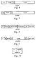
The format of the register iAPRsf is illustrated in FIG. 6. The register iAPRsf includes the fields res, mode, sc and count. The field res indicates that this portion of the register is reserved. The mode field is written to by the producer device when the space remaining within the small subframe buffer is not big enough to hold the next small frame of data or the producer device has sent the maximum number of small frames. The bit sc is a segment count bit and is set by the producer device to equal the most recent sc bit value written by the consumer device into the register oAPRsf at the producer device. The field count identifies how many bytes of data have been written by the producer device into the small subframe buffer of the consumer device.
The format of the register iAPRpf is illustrated in FIG. 7. The register iAPRpf includes the fields r, hb, mode, sc and count. The field r indicates that this portion of the register is reserved. The bit hb when written indicates that the contents of this register iAPRpf have been updated and provides an interrupt to the consumer device. The field mode is preferably a two-bit field which provides frame-completion information, as specified in Table I below.
TABLE I
Mode Name Description
0 FREE Initial state. Shall never be written by the
producer.
1 MORE Indication for leading (not end of frame, last)
content.
2 LAST Indication for last, end of frame content.
3 TRUNC Indication for truncated frame content, end of
frame.
The mode FREE is an initial state that is never written by the producer device. The mode MORE is an indication that for leading content that the end of the frame has not been transferred. The mode LAST is an indication that the end of the frame has been transferred. The mode TRUNC is an indication that the frame content has been truncated, but that the end of the frame has been transferred.
Within the register iAPRpf, the bit sc is a segment count bit and is set by the producer device to equal the most recent sc bit value written by the consumer device into the register oAPRpf at the producer device. The value within the field count identifies how many bytes have been written by the producer device to the scattered pages identified in the page table elements since the last update of the register iAPRpf.
The format of the register oAPRsf is illustrated in FIG. 8. The register oAPRsf includes the fields res, mode, sc, blockCount, byteCount, res and maxLoad. The two res fields indicate that these portions of the register are reserved. The bit mode is written by the consumer device when there is space available within the small subframe buffer. The bit sc is a segment count bit and is set by the consumer device. The value of the segment count bit sc is toggled by the consumer device on each successive write to the register oAPRsf. The value included within the field blockCount represents the limit of the number of subframe blocks that can be written to the small subframe buffer. The value included within the field byteCount represents the limit of the number of bytes that can be written to the small subframe buffer. The number of interrupting small frame write operations that will be permitted is limited by both the number of actual small frames that are written, if the small frames are much less than the capacity of the small subframe buffer, and the number of bytes that are written, if the small frames are closer to the capacity of the small subframe buffer. The value included within the field maxLoad represents the maximum number of small frames that a producer device can transmit to the consumer device before updating the register iAPRsf at the consumer device.
The format of the register oAPRpf is illustrated in FIG. 9. The register oAPRpf includes the fields r, hb, mode, sc, count, run, r and maxLoad. The two fields r indicate that these portions of the register are reserved. The bit hb when written indicates that the contents of this register oAPRpf have been updated by the consumer device. The bit mode is written by the consumer device when there is space available within the scattered pages to receive large frame transfers. The bit sc is a segment count bit and is set by the consumer device. The value of the segment count bit sc is toggled by the consumer device on each successive write to the register oAPRpf. The value included within the field count indicates the total number of bytes available within the scattered pages or buffers available to receive large frame transfers. The run bit enables the producer device to send large frames to the consumer device. When the value of the run bit is set to equal a logical high value, then the producer device is enabled to send large frames of data to the consumer device. When the value of the run bit is reset to equal a logical low value, then the producer device is inhibited from sending large frames of data to the consumer device. The value included within the field maxLoad represents the data-payload size limitations for individual, segment buffer write operations.
The format of the page table entries 46-50 is illustrated in FIG. 10. Each page table entry points to a consumer segment buffer or page of memory within the dedicated IEEE 1394 memory space of the consumer device. Use of the page table entries allows a consumer device to program a list of buffers or pages of memory in possibly non-contiguous memory space for use in large frame transfers from the producer device. Preferably, each of the page table entries include the fields size, offsetHi and offsetLo. The field size is a two byte field that contains a value indicating the size of the particular page of memory represented by the page table entry. The size of pages utilized by the consumer device to receive data within a large frame transfer can vary. However, each page of memory must provide a contiguous memory space. Preferably, each page of memory utilized for large frame transfers has a size of at least 4 Kbytes. The field offsetHi is a two byte field that contains the two highest order bytes of an offset address value. The field offsetLo is a four byte field that contains the four lowest order bytes of an offset address value. Together, the values within the fields offsetHi and offsetLo form the address offset value, used to specify the beginning address of the page of memory represented by the particular page table entry.
The scattered page tables at a consumer device and the corresponding page table entries programmed at a producer device can be utilized for transfers of data from a producer device to a consumer device through any appropriate plug, including simplex plugs, duplex plugs and dual-duplex plugs.
An IEEE 1394-1995 asynchronous write transaction is utilized to transfer data from a producer device to a consumer device over a 1394TA IICP connection. Within the IEEE 1394-1995 packet of data a transaction code (tcode) is utilized to specify the packet format and type of transaction that is to be performed on the packet. As described above, in the preferred embodiment of the present invention, two segment buffers are used to receive data at the consumer device. The first buffer is the small subframe buffer which is utilized to receive small frame buffers. Write operations to this small subframe buffer cause an interrupt to occur at the consumer device. The second buffer is the large frame buffer which is made up of the scattered memory pages specified in the page table entries. The producer device writes to the control register of the consumer device when the transfer of the large frame data is complete.
In an alternate embodiment, a single segment buffer is utilized by the consumer device to receive both small frames and large frames. The data within both the small frames and large frames is written to the memory page or pages specified by the page table entries. For the transfer of small frames only, the memory page corresponding to the first page table entry is used. Within this alternative embodiment, an extended transaction code is used in packets in which an interrupt should occur at the consumer device. Accordingly, in packets transmitting a small frame of data to the first memory page, this write with interrupt transaction code is included to cause an interrupt at the consumer device when the data is written. For large frame transfers, the write with interrupt transaction code is only used when the last packet of data within the large frame of data is being transferred.
In operation, the scattering memory page tables of the present invention allow a consumer device to specify discontiguous pages in memory which together form a large frame buffer to receive large frames of data from the producer device. The consumer device programs page table entries within the plug control register at the producer device specifying the addresses of the corresponding page table entries. When transferring a large frame of data, the producer device then transmits the data utilizing write operations to the successive memory pages, specified by the page table entries, as appropriate, until the transfer of the large frame of data is complete. When the producer device has completed the transfer of the large frame of data, the producer device then updates the register iAPRpf at the consumer device to inform the consumer device that the large frame transfer is complete. The consumer device then provides the data within the scattered memory pages of the large frame buffer to the appropriate application.
When ready to receive a small frame, the consumer device appropriately updates the fields within the connection register of the producer device. When the producer device then receives a request from an application layer to transfer a small frame of data, the producer device then transmits a write data packet to write the small frame data in the small frame buffer within the connection register of the consumer device. This write operation to the small frame buffer then causes an interrupt at the consumer device. In response to this interrupt, the consumer device then provides the small frame to the appropriate application.
The present invention has been described in terms of specific embodiments incorporating details to facilitate the understanding of the principles of construction and operation of the invention. Such reference herein to specific embodiments and details thereof is not intended to limit the scope of the claims appended hereto. It will be apparent to those skilled in the art that modifications can be made in the embodiment chosen for illustration without departing from the spirit and scope of the invention. Specifically, it will be apparent to one of ordinary skill in the art that the device of the present invention could be implemented in several different ways and the architecture, system and method disclosed above are only illustrative of preferred embodiments of the invention. Specifically, it will be apparent to those skilled in the art that while the preferred embodiment of the present invention is used with an IEEE 1394-1995 serial bus structure, the present invention could also be implemented on any other appropriate digital interfaces or bus structures, including other or later versions of the IEEE 1394 serial bus.

Claims (52)

We claim:
1. A method or transferring data between a transmitting device and a receiving device comprising the steps of:
a. sending a communication from the receiving device to the transmitting device including a notification that the receiving device is ready to receive data and a plurality of page table entries each corresponding to a location in memory or the receiving device to which the data is to be written;
b. transferring the data from the transmitting device to the receiving device in one or more transactions to successive ones of the locations in memory corresponding to the page table entries;
c. determining if a single transaction will include all of the data; and
d. transferring the data to a small frame buffer at the receiving device if it is determined that the single transaction will include all of the data.
2. The method as claimed in claim 1 further comprising the step of sending a notification from the transmitting device to the receiving device upon completion of transmission of the data.
3. The method as claimed in claim 1 wherein the transfer of data to the small frame buffer causes an interrupt to occur at the receiving device.
4. The method as claimed in claim 1 wherein the small frame buffer is a buffer within a plug control register.
5. The method as claimed in claim 1 wherein an address of the small frame buffer is specified by a designated one of the page table entries.
6. The method as claimed in claim 1 wherein the locations in memory corresponding to the page table entries are not contiguous.
7. The method as claimed in claim 1 wherein together the locations in memory corresponding to the page table entries form a large frame buffer.
8. The method as claimed in claim 1 wherein the page table entries are stored at the transmitting device in a control register.
9. The method as claimed in claim 1 further comprising the step of updating the page table entries before a transfer of a next frame.
10. A method of transferring data between a transmitting device and a receiving device comprising:
a. sending a communication from the receiving device to the transmitting device including a notification that the receiving device is ready to receive data and a plurality of page table entries each corresponding to a location in memory of the receiving device to which the data is to be written; and
b. transferring the data from the transmitting device to the receiving device in one or more transactions to successive ones of the locations in memory corresponding to the page table entries;
wherein the one or more transactions include an extended transaction code specifying whether or not an interrupt is to occur upon completion of the transaction.
11. The method as claimed in claim 10 wherein a final transaction within a frame of data includes the extended transaction code specifying that the interrupt is to occur upon completion of the transaction.
12. The method as claimed in claim 1 wherein the transmitting device and the receiving device are coupled together by an IEEE 1394 serial bus.
13. The method as claimed in claim 12 wherein the transmitting device and the receiving device operate according to a version of the 1394TA IICP specification.
14. A method of transferring data between a transmitting device and a receiving device comprising the steps of:
a. sending a small frame control communication from the receiving device to the transmitting device including a notification that the receiving device is ready to receive a small frame of data;
b. sending a large frame control communication from the receiving device to the transmitting device including a notification that the receiving device is ready to receive a large frame of data and a plurality of page table entries each corresponding to a location in memory of the receiving device to which portions of the large frame of data are to be written;
c. receiving a frame of data from an application at the transmitting device;
d. determining if the received frame of data is a small frame of data or a large frame of data;
e. transferring the received frame of data to a small frame buffer at the receiving device if it is determined that the received frame of data is a small frame of data; and
f. transferring the received frame of data from the transmitting device to the receiving device in multiple transactions to successive ones of the locations in memory corresponding to the page table entries if it is determined that the received frame of data is a large frame of data.
15. The method as claimed in claim 14 further comprising the step of sending a notification from the transmitting device to the receiving device upon completion of transmission of the large frame of data.
16. The method as claimed in claim 14 wherein the transfer of data to the small frame buffer causes an interrupt to occur at the receiving device.
17. The method as claimed in claim 14 wherein the small frame buffer is a buffer within a plug control register.
18. The method as claimed in claim 14 wherein an address of the small frame buffer is specified by a designated one of the page table entries.
19. The method as claimed in claim 14 wherein together the locations in memory corresponding to the page table entries form a large frame buffer.
20. The method as claimed in claim 14 wherein the locations in memory corresponding to the page table entries are not contiguous.
21. The method as claimed in claim 14 wherein the page table entries are stored at the transmitting device in a control register.
22. The method as claimed in claim 14 wherein a small frame of data is transferred in a single transaction and a large frame of data is transferred in more than one transaction.
23. The method as claimed in claim 14 further comprising the step of updating the page table entries before a transfer of a next frame.
24. The method as claimed in claim 14 wherein the transmitting device and the receiving device are coupled together by an IEEE 1394 serial bus.
25. The method as claimed in claim 24 wherein the transmitting device and the receiving device operate according to a version of the 1394TA IICP specification.
26. A transmitting device configured to transmit data to a receiving device comprising:
a. an interface configured for coupling to the receiving device to transmit frame data to the receiving device and receive control data from the receiving device; and
b. a register coupled to the interface to store the control data, wherein the register includes a plurality of page table entries which are programmed by the receiving device and hold address data corresponding to locations in memory of the receiving device to which a frame of data is to be written;
wherein the transmitting device transmits the frame of data to the receiving device in one or more transactions through the interface to successive ones of the locations in memory corresponding to the page table entries and further wherein the one or more transactions include an extended transaction code specifying whether or not an interrupt is to occur upon completion of the transaction.
27. The transmitting device as claimed in claim 26 wherein the locations in memory corresponding to the page table entries are not contiguous.
28. The transmitting device as claimed in claim 26 wherein together the locations in memory corresponding to the page table entries form a large frame buffer.
29. The transmitting device as claimed in claim 26 wherein the receiving device has the ability to update the page table entries between transfer of each frame.
30. The transmitting device as claimed in claim 26 wherein a final transaction within a frame of data includes the extended transaction code specifying that the interrupt is to occur upon completion of the transaction.
31. The transmitting device as claimed in claim 26 wherein the transmitting device is configured to transmit data to the receiving device over an IEEE 1394 serial bus.
32. The transmitting device as claimed in claim 31 wherein the transmitting device and the receiving device operate according to a version of the 1394TA IICP specification.
33. A receiving device configured to receive data from a transmitting device comprising:
a. an interface configured for coupling to the transmitting device to receive frame data from the transmitting device and transmit control data to the transmitting device;
b. a plurality of memory pages which together form a fame buffer, each of the memory pages having a corresponding address; and
c. a small frame buffer coupled to the interface for storing a small frame of data transmitted from the transmitting device in a single transaction;
wherein the receiving device transmits the control data to the transmitting device including the address of the plurality of memory pages and the transmitting device will transmit the frame data to the receiving device in one or more transactions through the interface to successive ones of the plurality of memory pages.
34. The receiving device as claimed in claim 33 wherein the small frame buffer is a buffer within a plug control register.
35. The receiving device as claimed in claim 33 wherein an address of the small frame buffer is specified by a designated one of the page table entries.
36. The receiving device as claimed in claim 33 wherein the locations of plurality of memory pages are not contiguous.
37. The receiving device as claimed in claim 33 wherein the page table entries are stored at the transmitting device in a control register.
38. The receiving device as claimed in claim 33 wherein the receiving device has the ability to update the page table entries between transfer of each frame.
39. A receiving device configured to receive data from a transmitting device comprising:
a. an interface configured for coupling to the transmitting device to receive frame data from the transmitting device and transmit control data to the transmitting device; and
b. a plurality of memory pages which together form a frame buffer, each of the memory pages having a corresponding address; and
wherein the receiving device transmits the control data to the transmitting device including the addresses of the plurality of memory pages and the transmitting device will transmit the frame data to the receiving device in one or more transactions through the interface to successive ones of the plurality of memory pages and further wherein the one or more transactions include an extended transaction code specifying whether or not an interrupt is to occur upon completion of the transaction.
40. The receiving device as claimed in claim 39 wherein a final transaction within a frame of data includes the extended transaction code specifying that the interrupt is to occur upon completion of the transaction.
41. The receiving device as claimed in claim 33 wherein the transmitting device is configured to transmit data to the receiving device over an IEEE 1394 serial bus.
42. The receiving device as claimed in claim 41 wherein the transmitting device and the receiving device operate according to a version of the 1394TA IICP specification.
43. A communication system comprising:
a. a transmitting device including:
i. a first interface for transmitting frame data and receiving control data; and
ii. a first control register coupled to the first interface to store the control data including a plurality of page table entries; and
b. a receiving device including:
i. a second interface coupled to the first interface to receive the frame data from the transmitting device and transmit control data to the transmitting device;
ii. a second control register coupled to the second interface; and
iii. a plurality of memory pages which together form a large frame buffer, each of the memory pages having a corresponding address, wherein the receiving device transmits the control data to the transmitting device including the addresses of the plurality of memory pages which are stored in the plurality of page table entries and further wherein the transmitting device transmits the frame data to the receiving device in one or more transactions to be written into successive ones of the plurality of memory pages.
44. The communication system as claimed in claim 43 wherein the receiving device further comprises a small frame buffer coupled to the second interface for storing a small frame of data transmitted from the transmitting device in a single transaction.
45. The communication system as claimed in claim 44 wherein the small frame buffer is included within the second control register.
46. The communication system as claimed in claim 44 wherein an address of the small frame buffer is specified by a designated one of the page table entries.
47. The communication system as claimed in claim 43 wherein the plurality of memory pages are not contiguous.
48. The communication system as claimed in claim 43 wherein the receiving device has the ability to update the page table entries between transfer of each frame.
49. The communication system as claimed in claim 43 wherein the one or more transactions include an extended transaction code specifying whether or not an interrupt is to occur upon completion of the transaction.
50. The communication system as claimed in claim 49 wherein a final transaction within a frame of data includes the extended transaction code specifying that the interrupt is to occur upon completion of the transaction.
51. The communication system as claimed in claim 43 wherein the first and second interfaces are coupled together by an IEEE 1394 serial bus.
52. The communication system as claimed in claim 51 wherein the transmitting device and the receiving device both operate according to a version of the 1394TA IICP specification.
US09/548,050 1999-04-12 2000-04-12 Asynchronous connections with scattering page tables for transmitting data from a producer device to a consumer device over an IEEE 1394 serial data bus Expired - Fee Related US6421745B1 (en)

Priority Applications (3)

Application Number Priority Date Filing Date Title
US09/548,050 US6421745B1 (en) 1999-04-12 2000-04-12 Asynchronous connections with scattering page tables for transmitting data from a producer device to a consumer device over an IEEE 1394 serial data bus
AU42381/00A AU4238100A (en) 1999-04-12 2000-04-12 Asynchronous data transmission with scattering page tables
PCT/US2000/009920 WO2000062179A1 (en) 1999-04-12 2000-04-12 Asynchronous data transmission with scattering page tables

Applications Claiming Priority (2)

Application Number Priority Date Filing Date Title
US12888199P 1999-04-12 1999-04-12
US09/548,050 US6421745B1 (en) 1999-04-12 2000-04-12 Asynchronous connections with scattering page tables for transmitting data from a producer device to a consumer device over an IEEE 1394 serial data bus

Publications (1)

Publication Number Publication Date
US6421745B1 true US6421745B1 (en) 2002-07-16

Family

ID=26827038

Family Applications (1)

Application Number Title Priority Date Filing Date
US09/548,050 Expired - Fee Related US6421745B1 (en) 1999-04-12 2000-04-12 Asynchronous connections with scattering page tables for transmitting data from a producer device to a consumer device over an IEEE 1394 serial data bus

Country Status (3)

Country Link
US (1) US6421745B1 (en)
AU (1) AU4238100A (en)
WO (1) WO2000062179A1 (en)

Cited By (6)

* Cited by examiner, † Cited by third party
Publication number Priority date Publication date Assignee Title
US6629159B1 (en) * 1999-07-31 2003-09-30 Lg Electronics Inc. Method for modifying data of specific register in digital interface
US20030198238A1 (en) * 2002-04-19 2003-10-23 Seagate Technology Llc Prioritizing outbound data transfers across a serial data transmission interface
US20040170193A1 (en) * 2003-02-28 2004-09-02 Schauer Steven A. Large transmissions on packetized data bus
US20050182886A1 (en) * 2004-02-17 2005-08-18 Edirisooriya Geetani R. Method and apparatus for supporting multi-function PCI devices in PCI bridges
US7222221B1 (en) * 2004-02-06 2007-05-22 Vmware, Inc. Maintaining coherency of derived data in a computer system
US20200192857A1 (en) * 2018-12-18 2020-06-18 Sap Se Remote memory management

Citations (23)

* Cited by examiner, † Cited by third party
Publication number Priority date Publication date Assignee Title
US4713702A (en) 1983-09-05 1987-12-15 Sony Corporation Data communication apparatus
US4930065A (en) * 1987-08-20 1990-05-29 David Computer Corporation Automatic data channels for a computer system
EP0428111A2 (en) 1989-11-14 1991-05-22 Hitachi, Ltd. Data transfer control method and data processor using the same
US5315705A (en) 1991-02-25 1994-05-24 Hitachi, Ltd. Communication address management system
US5408501A (en) 1993-04-06 1995-04-18 Conner Peripherals, Inc. Data transfer system
US5434860A (en) 1994-04-20 1995-07-18 Apple Computer, Inc. Flow control for real-time data streams
US5444709A (en) 1993-09-30 1995-08-22 Apple Computer, Inc. Protocol for transporting real time data
US5448698A (en) 1993-04-05 1995-09-05 Hewlett-Packard Company Inter-processor communication system in which messages are stored at locations specified by the sender
US5517494A (en) 1994-09-30 1996-05-14 Apple Computer, Inc. Method and system of multicast routing for groups with a single transmitter
US5519701A (en) 1995-03-29 1996-05-21 International Business Machines Corporation Architecture for high performance management of multiple circular FIFO storage means
US5619544A (en) 1994-06-03 1997-04-08 Texas Instruments Incorporated Universal asynchronous receive/transmit circuit with flow control
US5661848A (en) 1994-09-08 1997-08-26 Western Digital Corp Multi-drive controller with encoder circuitry that generates ECC check bytes using the finite field for optical data for appending to data flowing to HDA
US5668952A (en) 1994-08-08 1997-09-16 International Business Machines Corporation Method for resolving network address by sending reresolve request to nodes at selected time period after establishing address table, and updating the table with received reply thereto
US5729755A (en) 1991-09-04 1998-03-17 Nec Corporation Process for transmitting data in a data processing system with distributed computer nodes, communicating via a serial data bus, between which data messages are exchanged, tested for acceptance in a computer node, and stored temporarily
US5748911A (en) 1996-07-19 1998-05-05 Compaq Computer Corporation Serial bus system for shadowing registers
US5758075A (en) 1994-07-29 1998-05-26 International Business Machines Corporation Multimedia communication apparatus and methods
US5815668A (en) 1995-03-17 1998-09-29 Nec Corporation Slave inter-lan connection device, an inter-lan connection system and a hot standby method of said inter-lan connection system
US5835725A (en) 1996-10-21 1998-11-10 Cisco Technology, Inc. Dynamic address assignment and resolution technique
US5867656A (en) 1992-09-25 1999-02-02 Hitachi, Ltd. Method for interprocessor communication
US5940592A (en) 1995-03-03 1999-08-17 Hitachi, Ltd. Communication processing method in parallel computer and system therefor
US5941964A (en) 1992-05-21 1999-08-24 Intel Corporation Bridge buffer management by bridge interception of synchronization events
US5991520A (en) 1996-02-02 1999-11-23 Sony Corporation Application programming interface for managing and automating data transfer operations between applications over a bus structure
US6034964A (en) 1996-06-11 2000-03-07 Hitachi, Ltd. Router device and network system using the same

Patent Citations (23)

* Cited by examiner, † Cited by third party
Publication number Priority date Publication date Assignee Title
US4713702A (en) 1983-09-05 1987-12-15 Sony Corporation Data communication apparatus
US4930065A (en) * 1987-08-20 1990-05-29 David Computer Corporation Automatic data channels for a computer system
EP0428111A2 (en) 1989-11-14 1991-05-22 Hitachi, Ltd. Data transfer control method and data processor using the same
US5315705A (en) 1991-02-25 1994-05-24 Hitachi, Ltd. Communication address management system
US5729755A (en) 1991-09-04 1998-03-17 Nec Corporation Process for transmitting data in a data processing system with distributed computer nodes, communicating via a serial data bus, between which data messages are exchanged, tested for acceptance in a computer node, and stored temporarily
US5941964A (en) 1992-05-21 1999-08-24 Intel Corporation Bridge buffer management by bridge interception of synchronization events
US5867656A (en) 1992-09-25 1999-02-02 Hitachi, Ltd. Method for interprocessor communication
US5448698A (en) 1993-04-05 1995-09-05 Hewlett-Packard Company Inter-processor communication system in which messages are stored at locations specified by the sender
US5408501A (en) 1993-04-06 1995-04-18 Conner Peripherals, Inc. Data transfer system
US5444709A (en) 1993-09-30 1995-08-22 Apple Computer, Inc. Protocol for transporting real time data
US5434860A (en) 1994-04-20 1995-07-18 Apple Computer, Inc. Flow control for real-time data streams
US5619544A (en) 1994-06-03 1997-04-08 Texas Instruments Incorporated Universal asynchronous receive/transmit circuit with flow control
US5758075A (en) 1994-07-29 1998-05-26 International Business Machines Corporation Multimedia communication apparatus and methods
US5668952A (en) 1994-08-08 1997-09-16 International Business Machines Corporation Method for resolving network address by sending reresolve request to nodes at selected time period after establishing address table, and updating the table with received reply thereto
US5661848A (en) 1994-09-08 1997-08-26 Western Digital Corp Multi-drive controller with encoder circuitry that generates ECC check bytes using the finite field for optical data for appending to data flowing to HDA
US5517494A (en) 1994-09-30 1996-05-14 Apple Computer, Inc. Method and system of multicast routing for groups with a single transmitter
US5940592A (en) 1995-03-03 1999-08-17 Hitachi, Ltd. Communication processing method in parallel computer and system therefor
US5815668A (en) 1995-03-17 1998-09-29 Nec Corporation Slave inter-lan connection device, an inter-lan connection system and a hot standby method of said inter-lan connection system
US5519701A (en) 1995-03-29 1996-05-21 International Business Machines Corporation Architecture for high performance management of multiple circular FIFO storage means
US5991520A (en) 1996-02-02 1999-11-23 Sony Corporation Application programming interface for managing and automating data transfer operations between applications over a bus structure
US6034964A (en) 1996-06-11 2000-03-07 Hitachi, Ltd. Router device and network system using the same
US5748911A (en) 1996-07-19 1998-05-05 Compaq Computer Corporation Serial bus system for shadowing registers
US5835725A (en) 1996-10-21 1998-11-10 Cisco Technology, Inc. Dynamic address assignment and resolution technique

Non-Patent Citations (3)

* Cited by examiner, † Cited by third party
Title
"The IEEE-1394 High Speed Serial Bus," R.H.J. Bloks, Philips Journal Of Research, vol. 50, No. 1/2, pp. 209-216, 1996.
Michael Teener et al., "A Bus on a Diet-The Serial Bus Alternative, An Introduction to the P1394 High performance Serial Bus" Apple Computer, Inc. Santa Clara, CA, Pub. Date.: Feb. 24, 1992, pp. 316-321.
P134 Standard For A High Performance Serial Bus, IEEE, 1995.

Cited By (11)

* Cited by examiner, † Cited by third party
Publication number Priority date Publication date Assignee Title
US6629159B1 (en) * 1999-07-31 2003-09-30 Lg Electronics Inc. Method for modifying data of specific register in digital interface
US20030198238A1 (en) * 2002-04-19 2003-10-23 Seagate Technology Llc Prioritizing outbound data transfers across a serial data transmission interface
US7359397B2 (en) 2002-04-19 2008-04-15 Seagate Technology Llc Prioritizing transfers across an interface
US20040170193A1 (en) * 2003-02-28 2004-09-02 Schauer Steven A. Large transmissions on packetized data bus
US7609725B2 (en) * 2003-02-28 2009-10-27 Lsi Corporation Large transmissions on packetized data bus
US7222221B1 (en) * 2004-02-06 2007-05-22 Vmware, Inc. Maintaining coherency of derived data in a computer system
US7783838B1 (en) 2004-02-06 2010-08-24 Vmware, Inc. Maintaining coherency of derived data in a computer system
US20050182886A1 (en) * 2004-02-17 2005-08-18 Edirisooriya Geetani R. Method and apparatus for supporting multi-function PCI devices in PCI bridges
US7213094B2 (en) * 2004-02-17 2007-05-01 Intel Corporation Method and apparatus for managing buffers in PCI bridges
US20200192857A1 (en) * 2018-12-18 2020-06-18 Sap Se Remote memory management
US11379404B2 (en) * 2018-12-18 2022-07-05 Sap Se Remote memory management

Also Published As

Publication number Publication date
AU4238100A (en) 2000-11-14
WO2000062179A1 (en) 2000-10-19

Similar Documents

Publication Publication Date Title
EP0885418B1 (en) Asynchronous data pipe for automatically managing asynchronous data transfers between an application and a bus structure
US6651119B2 (en) Method for allocating priorities to plurality of DMA engines for processing data packets based on bus phase and transactions status
US6141767A (en) Method of and apparatus for verifying reliability of contents within the configuration ROM of IEEE 1394-1995 devices
US7590133B2 (en) Data communication system, data communication method, and data communication apparatus
US6516361B2 (en) Method of and apparatus for capturing and processing continuous media-based data streams transmitted over an IEEE 1394 serial bus
KR100605657B1 (en) Method and apparatus for processing received data, and receiving device for receiving data from one or more remote devices
EP0939529B1 (en) Destination node, data communication system, method of controlling a destination node and method of operating a data communication system
US6363428B1 (en) Apparatus for and method of separating header information from data in an IEEE 1394-1995 serial bus network
US6298406B1 (en) Method of and apparatus for detecting direction of reception of bus packets and controlling direction of transmission of bus packets within an IEEE 1394 serial bus node
US6721859B1 (en) Multi-protocol media storage device implementing protocols optimized for storing and retrieving both asynchronous and isochronous data
US6421745B1 (en) Asynchronous connections with scattering page tables for transmitting data from a producer device to a consumer device over an IEEE 1394 serial data bus
US6041286A (en) Apparatus for and method of accurately obtaining the cycle time of completion of transmission of video frames within an isochronous stream of data transmitted over an IEEE 1394 serial bus network
KR100311707B1 (en) Data communication system, data communication method, data communication apparatus, and digital interface
US6993022B1 (en) Method of and apparatus for directly mapping communications through a router between nodes on different buses within a network of buses
US6366590B2 (en) Unified interface between an IEEE 1394-1995 serial bus transaction layer and corresponding applications
KR20010033660A (en) Data transfer controller and electronic device
US7003604B2 (en) Method of and apparatus for cancelling a pending AV/C notify command
US6256698B1 (en) Method of and apparatus for providing self-sustained even arbitration within an IEEE 1394 serial bus network of devices
JP2002135270A (en) Data asynchronous transfer system
EP1228436A1 (en) Device for storing audio/video data and non audio/video data

Legal Events

Date Code Title Description
AS Assignment

Owner name: SONY CORPORATION, JAPAN

Free format text: ASSIGNMENT OF ASSIGNORS INTEREST;ASSIGNORS:JAMES, DAVID V.;SHIMA, HISATO;FAIRMAN, BRUCE;REEL/FRAME:011168/0770;SIGNING DATES FROM 20000726 TO 20000827

Owner name: SONY ELECTRONICS, INC., NEW JERSEY

Free format text: ASSIGNMENT OF ASSIGNORS INTEREST;ASSIGNORS:JAMES, DAVID V.;SHIMA, HISATO;FAIRMAN, BRUCE;REEL/FRAME:011168/0770;SIGNING DATES FROM 20000726 TO 20000827

CC Certificate of correction
FPAY Fee payment

Year of fee payment: 4

FPAY Fee payment

Year of fee payment: 8

REMI Maintenance fee reminder mailed
LAPS Lapse for failure to pay maintenance fees
STCH Information on status: patent discontinuation

Free format text: PATENT EXPIRED DUE TO NONPAYMENT OF MAINTENANCE FEES UNDER 37 CFR 1.362

FP Lapsed due to failure to pay maintenance fee

Effective date: 20140716