US6424668B1 - Semiconductor laser device having an SBR structure - Google Patents
Semiconductor laser device having an SBR structure Download PDFInfo
- Publication number
- US6424668B1 US6424668B1 US09/351,803 US35180399A US6424668B1 US 6424668 B1 US6424668 B1 US 6424668B1 US 35180399 A US35180399 A US 35180399A US 6424668 B1 US6424668 B1 US 6424668B1
- Authority
- US
- United States
- Prior art keywords
- layer
- ridge
- upper cladding
- semiconductor laser
- cladding layer
- Prior art date
- Legal status (The legal status is an assumption and is not a legal conclusion. Google has not performed a legal analysis and makes no representation as to the accuracy of the status listed.)
- Expired - Fee Related
Links
Images


Classifications
-
- H—ELECTRICITY
- H01—ELECTRIC ELEMENTS
- H01S—DEVICES USING THE PROCESS OF LIGHT AMPLIFICATION BY STIMULATED EMISSION OF RADIATION [LASER] TO AMPLIFY OR GENERATE LIGHT; DEVICES USING STIMULATED EMISSION OF ELECTROMAGNETIC RADIATION IN WAVE RANGES OTHER THAN OPTICAL
- H01S5/00—Semiconductor lasers
- H01S5/30—Structure or shape of the active region; Materials used for the active region
-
- H—ELECTRICITY
- H01—ELECTRIC ELEMENTS
- H01S—DEVICES USING THE PROCESS OF LIGHT AMPLIFICATION BY STIMULATED EMISSION OF RADIATION [LASER] TO AMPLIFY OR GENERATE LIGHT; DEVICES USING STIMULATED EMISSION OF ELECTROMAGNETIC RADIATION IN WAVE RANGES OTHER THAN OPTICAL
- H01S5/00—Semiconductor lasers
- H01S5/20—Structure or shape of the semiconductor body to guide the optical wave ; Confining structures perpendicular to the optical axis, e.g. index or gain guiding, stripe geometry, broad area lasers, gain tailoring, transverse or lateral reflectors, special cladding structures, MQW barrier reflection layers
- H01S5/22—Structure or shape of the semiconductor body to guide the optical wave ; Confining structures perpendicular to the optical axis, e.g. index or gain guiding, stripe geometry, broad area lasers, gain tailoring, transverse or lateral reflectors, special cladding structures, MQW barrier reflection layers having a ridge or stripe structure
- H01S5/223—Buried stripe structure
- H01S5/2231—Buried stripe structure with inner confining structure only between the active layer and the upper electrode
-
- H—ELECTRICITY
- H01—ELECTRIC ELEMENTS
- H01S—DEVICES USING THE PROCESS OF LIGHT AMPLIFICATION BY STIMULATED EMISSION OF RADIATION [LASER] TO AMPLIFY OR GENERATE LIGHT; DEVICES USING STIMULATED EMISSION OF ELECTROMAGNETIC RADIATION IN WAVE RANGES OTHER THAN OPTICAL
- H01S5/00—Semiconductor lasers
- H01S5/20—Structure or shape of the semiconductor body to guide the optical wave ; Confining structures perpendicular to the optical axis, e.g. index or gain guiding, stripe geometry, broad area lasers, gain tailoring, transverse or lateral reflectors, special cladding structures, MQW barrier reflection layers
- H01S5/2004—Confining in the direction perpendicular to the layer structure
-
- H—ELECTRICITY
- H01—ELECTRIC ELEMENTS
- H01S—DEVICES USING THE PROCESS OF LIGHT AMPLIFICATION BY STIMULATED EMISSION OF RADIATION [LASER] TO AMPLIFY OR GENERATE LIGHT; DEVICES USING STIMULATED EMISSION OF ELECTROMAGNETIC RADIATION IN WAVE RANGES OTHER THAN OPTICAL
- H01S5/00—Semiconductor lasers
- H01S5/30—Structure or shape of the active region; Materials used for the active region
- H01S5/32—Structure or shape of the active region; Materials used for the active region comprising PN junctions, e.g. hetero- or double- heterostructures
- H01S5/323—Structure or shape of the active region; Materials used for the active region comprising PN junctions, e.g. hetero- or double- heterostructures in AIIIBV compounds, e.g. AlGaAs-laser, InP-based laser
- H01S5/32308—Structure or shape of the active region; Materials used for the active region comprising PN junctions, e.g. hetero- or double- heterostructures in AIIIBV compounds, e.g. AlGaAs-laser, InP-based laser emitting light at a wavelength less than 900 nm
- H01S5/32325—Structure or shape of the active region; Materials used for the active region comprising PN junctions, e.g. hetero- or double- heterostructures in AIIIBV compounds, e.g. AlGaAs-laser, InP-based laser emitting light at a wavelength less than 900 nm red laser based on InGaP
Landscapes
- Physics & Mathematics (AREA)
- Condensed Matter Physics & Semiconductors (AREA)
- General Physics & Mathematics (AREA)
- Electromagnetism (AREA)
- Optics & Photonics (AREA)
- Geometry (AREA)
- Semiconductor Lasers (AREA)
Abstract
A semiconductor laser device includes a substrate formed of GaAs. A lower electrode is formed on an underside of this substrate. Formed, on a top surface of the substrate, are a lower cladding layer, an active layer and a first upper cladding layer. A ridge including a second upper cladding layer is formed on the first upper cladding layer. A current restricting layer is formed in a manner of clamping this ridge from both sides. A contact layer is formed on the ridge and current restricting layer. A third upper cladding layer is formed between the ridge and current restricting layer and the contact layer.
Description
1. Field of the Invention
This invention relates to semiconductor laser devices and, more particularly, to a semiconductor laser device of an SBR (Selected Buried Ridge stripe) structure used for digital video discs, magnet-optical discs, laser printers, and the like.
2. Description of the Prior Art
A conventional semiconductor laser device 1 of this kind, as shown in FIG. 3, includes a substrate. On the substrate 2 are formed a buffer layer 3, a lower cladding layer 4 a, an active layer 5, a first upper cladding layer 4 b and an etch stop layer 6, in this order. A ridge 8 a is formed on the etch stop layer 6 by conducting etching after crystal growth. This ridge 8 a includes a second cladding layer 4 c and an intermediate contact layer 7 a. A current restricting layer 8 b is formed on the etch stop layer 6 in a manner clamping the ridge 8 a from both sides. A GaAs contact layer 7 b is formed on the ridge 8 a as well as current restricting layer 8 b. Further, electrodes 9 a and 9 b are formed respectively on an underside of the substrate 2 and on a top surface of the GaAs contact layer 7 b.
In an attempt to make this semiconductor laser device 1 compatible with an increase in output power, if the light in the active layer 5 is allowed to partly outdiffuse, the light density within the active layer 5 will be decreased. In such a case, if the outdiffused light from the active layer 5 reaches the optical-absorbent GaAs contact layer 7 b and is absorbed by the same layer, the semiconductor laser device 1 possibly deteriorates in characteristics. Due to this, it has been a conventional practice to increase the wall thickness of the ridge 8 a, thereby increasing a distance L between the active layer 5 and the GaAs contact layer 7 b and hence preventing the light from arriving at the GaAs contact layer 7 b.
In the prior art, the deterioration in laser characteristic resulting from output power increase has been prevented by thus increasing the wall thickness of the ridge 8 a. This, however, has resulted in an increase in side etch amount on the ridge 8 a upon implementing an etching process for providing the ridge 8 a, resulting in narrowed top end width (current passage width) of the ridge 8 a. Thus, there has been a problem that the device is increased in series resistance leading to an increase in operating voltage.
Therefore, it is a primary object of the present invention to provide a novel semiconductor laser device.
It is another object of the present invention to provide a semiconductor laser device having an SBR structure which can prevent against degradation in laser characteristic due to increase of output without incurring increase in device series resistance.
A semiconductor laser device according to the present invention, comprises: a substrate; a lower cladding layer, an active layer and a first upper cladding layer which are formed in order on the substrate; a ridge formed on the first upper cladding layer, the ridge including a second upper cladding layer; a current restricting layer formed in a manner clamping the ridge; a contact layer formed on the ridge and the current restricting layer; and a third upper cladding layer formed between the ridge and current restricting layer and said contact layer.
The distance of from the active layer to the contact layer is secured sufficiently long by thus forming the third upper cladding layer between the ridge and current restricting layer and the contact layer. Consequently, there is no fear that the outdiffused light from the active layer arrive at the contact layer.
According to the present invention, because there is no need to increase the thickness of the ridge as conventionally done, it is possible to prevent the width of a ridge top end from being narrowed due to side over-etch on the ridge. Thus, the deterioration in laser characteristic due to output power increase can be prevented without incurring increase in series resistance.
The above described objects and other objects, features, aspects and advantages of the present invention will become more apparent from the following detailed description of the present invention when taken in conjunction with the accompanying drawings.
FIG. 1 is an illustrative view showing one embodiment of the present invention;
FIG. 2A-FIG. 2E are illustrative views showing a manufacturing process for the FIG. 1 embodiment; and
FIG. 3 is an illustrative view showing a prior art.
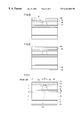
A semiconductor laser device 10 of this embodiment, shown in FIG. 1, includes an n-type substrate formed, for example, of GaAs. On an underside of the substrate 12, a lower electrode 14 is formed based on Au.
On the other hand, the substrate 12 has, on a top surface, an n-type buffer layer 16 formed for example of GaAs, an n-type lower cladding layer 18 formed for example of InGaAIP, an active layer 20 formed for example of InGaP/InGaAlP, such as Inz Ga1−zyAlyP where (0≦y≦1) (0<z<1), a p-type first upper cladding layer 22 for example of InGaAIP, and a p-type edge stop layer for example of InGaP, in this order.
On the etch stop layer 24, a ridge 30 is formed to have a p-type second upper cladding layer 26 formed for example of InGaAlP and a p-type intermediate contact layer 28 formed for example of InGaP. An n-type current restricting layer 32 is formed for example of GaAs in a manner of clamping this ridge 30.
On the ridge 30 and current restricting layer 32, formed are a p-type third cladding layer 34 for example of InGa1−XAlXP(0.4≦X≦1), a p-type intermediate bandgap layer 36 for example of InGaP and a contact layer 38 of an optical absorbent such as GaAs. An upper electrode 40 is formed based on Au on a top surface of the contact layer 38. Consequently, the active layer 20, has a corresponding portion to the ridge 30 which acts as an optical waveguide 20 a to produce and guide laser light therein.
Explanation will be made below on a method for concretely manufacturing a semiconductor laser device 10, wKith reference to FIG. 2A-FIG. 2E.
First, formed overlying a substrate 12, as shown in FIG. 2A, are a buffer layer 16 to a thickness of 100-200 Å, a lower cladding layer to 18-1.3 μm, an active layer 20 to 500-1000 Å, a first upper cladding layer 22 to 2000-4000 Å, an etch stop layer 24 to 100-300 Å, a second upper cladding layer 26 to 0.6-1.5 μm, and an intermediate contact layer 28 to 100-300 Å, by a Metal Organic Chemical Vapor Deposition process (hereinafter referred to as “MOCVD process”) or Molecular Beam Epitaxial growth process (hereinafter referred to as “MBE process”).
Then, as shown in FIG. 2B, a mask 42 of an SiO2 film is formed in a stripe form on the intermediate contact layer 28 by using a photolithographic technique. Using this mask 42, etching is conducted on the intermediate contact layer 28 and second upper cladding layer 26 to form them into a ridge 30. At this time, the edge stop layer 24 serves as a block against etching. Accordingly, undesirable etching does not occur on the first upper cladding layer 22.
Then, as shown in FIG. 2C, a current restricting layer 32 is formed overlying the edge stop layer 24 up to a height equivalent to a top surface of the ridge 30, by an MOCVD or MBE process.
Subsequently, the mask 42 is removed away. Thereafter, formed on the ridge 30 and current restricting layer 32, as shown in FIG. 2D, a third upper cladding layer 34 to a thickness of 0.3-1.0 μm, an intermediate bandgap layer 36 to 300-1000 Å, and a contact layer 38 to 0.5-3 μm, by the MOCVD or MBE process.
Thereafter, as shown in FIG. 2E, a lower electrode 14 is formed on an underside of the substrate 12 by evaporation or the like, while an upper electrode 40 is formed on a top surface of the contact layer 38 by evaporation or the like.
With the semiconductor laser device 10, if a voltage is applied to the lower electrode 14 and upper electrode 40, an electric current is injected from the upper electrode 40 through the contact layer 38, the ridge 30 and the like into the active layer 20. Thereupon, laser oscillation occurs at the underneath of the ridge 30, i.e. within the optical waveguide 20 a, thereby producing laser light. This light is allowed to partly outdiffuse into a region “A” shown by hatching in FIG. 1(B), thereby attaining increase of power output.
The light outdiffused from the optical waveguide 20 a, if reached and absorbed by the CaAs substrate 12 or the contact layer 38 and absorbed therein, would induce deterioration in laser characteristic, as described before. In this embodiment, however, the lower cladding layer 18 and the third upper cladding layer 34 are controlled in thickness during the crystal growth process (FIG. 2A, FIG. 2D). Due to this, it is possible to obtain respective distances L of from the active layer 20 to the GaAs substrate 12 and to the contact layer 38 sufficiently long for preventing against light arrival to them. Incidentally, because the dimensions of the region “A” (FIG. 1(B)) are varied depending upon an output of the semiconductor laser device 10, the distances L may be set optimal for that output.
According to this embodiment, there is no need to increase the thickness of the ridge 30 in order to prevent light absorption by the GaAs substrate 12 and contact layer 38. This can prevent against sidel over-etch on the ridge 30 and hence decrease in the width H of the ridge top end. Consequently, it is possible to prevent against deterioration in laser characteristics resulting from increase of power output without causing increase of series resistance.
Meanwhile, it is possible to set comparatively freely a thickness of the second cladding layer 26 constituting the ridge 30. This improves the freedom of design and makes it possible to apply the invention also to a self-oscillation laser.
Furthermore, because the intermediate bandgap layer 36 is formed between the third upper cladding layer 34 and the contact layer 38, the current given by the electrode 40 smoothly flows from the contact layer 38 to the third upper cladding layer 34.
Although the present invention has been described and illustrated in detail, it is clearly understood that the same is by way of illustration and example only and is not to be taken by way of limitation, the spirit and scope of the present invention being limited only by the terms of the appended claims.
Claims (6)
1. A semiconductor laser device, comprising:
a substrate;
a lower cladding layer, an active layer, a first upper cladding layer and an etch stop layer which are formed in order on said substrate, said active layer being for laser oscillation therein;
a ridge formed on said etch stop layer, said ridge including a second upper cladding layer and an intermediate contact layer on a top thereof;
a current restricting layer formed on both sides of said ridge;
a contact layer formed on said intermediate contact layer of said ridge and said current restricting layer; and
a third upper cladding layer formed between said contact layer and both of said intermediate contact layer of said ridge and said current restricting layer.
2. A semiconductor laser device according to claim 1 , wherein said contact layer is an optical absorbent.
3. A semiconductor laser device according to claim 1 , further comprising an intermediate bandgap layer formed between said third upper cladding layer and said contact layer.
4. A semiconductor laser device according to claim 2 , further comprising an intermediate bandgap layer formed between said third upper cladding layer and said contact layer.
5. A semiconductor device according to claim 1 , wherein said active layer includes In, Ga, Al, and P.
6. A semiconductor device according to claim 1 , wherein said active layer is formed of InzGa1−zyAlyP where (0≦y≦1) (0<z<1).
Applications Claiming Priority (2)
| Application Number | Priority Date | Filing Date | Title |
|---|---|---|---|
| JP10-200435 | 1998-07-15 | ||
| JP10200435A JP2000031585A (en) | 1998-07-15 | 1998-07-15 | Semiconductor laser device |
Publications (1)
| Publication Number | Publication Date |
|---|---|
| US6424668B1 true US6424668B1 (en) | 2002-07-23 |
Family
ID=16424253
Family Applications (1)
| Application Number | Title | Priority Date | Filing Date |
|---|---|---|---|
| US09/351,803 Expired - Fee Related US6424668B1 (en) | 1998-07-15 | 1999-07-13 | Semiconductor laser device having an SBR structure |
Country Status (3)
| Country | Link |
|---|---|
| US (1) | US6424668B1 (en) |
| JP (1) | JP2000031585A (en) |
| KR (1) | KR20000011496A (en) |
Cited By (5)
| Publication number | Priority date | Publication date | Assignee | Title |
|---|---|---|---|---|
| US20030007530A1 (en) * | 2001-06-26 | 2003-01-09 | Sharp Kabushiki Kaisha | Semiconductor laser element and process for producing the same |
| US6546033B2 (en) * | 2000-10-31 | 2003-04-08 | Fuji Photo Film Co., Ltd. | InGaAsP semiconductor laser device in which near-edge portions are filled with non-absorbent layer, and lower optical waveguide layer includes InGaP intermediate layer |
| US20040108508A1 (en) * | 2002-11-06 | 2004-06-10 | Mitsubishi Denki Kabushiki Kaisha | Semiconductor laser device |
| US20040114651A1 (en) * | 2002-03-15 | 2004-06-17 | Kabushiki Kaisha Toshiba | Semiconductor laser and method for manufacturing the same |
| US6826217B2 (en) * | 2001-08-13 | 2004-11-30 | Rohm Co., Ltd. | Semiconductor laser device |
Families Citing this family (2)
| Publication number | Priority date | Publication date | Assignee | Title |
|---|---|---|---|---|
| JP2003078208A (en) * | 2001-08-31 | 2003-03-14 | Toshiba Corp | Semiconductor laser device and its manufacturing method |
| JP4462193B2 (en) | 2006-01-13 | 2010-05-12 | ソニー株式会社 | Semiconductor device, semiconductor device inspection method, and semiconductor device inspection device |
Citations (4)
| Publication number | Priority date | Publication date | Assignee | Title |
|---|---|---|---|---|
| US5592502A (en) * | 1993-10-22 | 1997-01-07 | Sharp Kabushiki Kaisha | Semiconductor laser element and method for adjusting self-induced oscillation intensity of the same |
| US5619520A (en) * | 1994-09-09 | 1997-04-08 | Matsushita Electric Industrial Co., Ltd. | Semiconductor laser |
| US6009112A (en) * | 1994-09-16 | 1999-12-28 | Rohm Co., Ltd. | Semiconductor laser and manufacturing method therefor |
| US6118800A (en) * | 1996-03-01 | 2000-09-12 | Matsushita Electric Industrial Co., Ltd. | Semiconductor laser and cleaving method |
-
1998
- 1998-07-15 JP JP10200435A patent/JP2000031585A/en active Pending
-
1999
- 1999-07-06 KR KR1019990026984A patent/KR20000011496A/en active Search and Examination
- 1999-07-13 US US09/351,803 patent/US6424668B1/en not_active Expired - Fee Related
Patent Citations (4)
| Publication number | Priority date | Publication date | Assignee | Title |
|---|---|---|---|---|
| US5592502A (en) * | 1993-10-22 | 1997-01-07 | Sharp Kabushiki Kaisha | Semiconductor laser element and method for adjusting self-induced oscillation intensity of the same |
| US5619520A (en) * | 1994-09-09 | 1997-04-08 | Matsushita Electric Industrial Co., Ltd. | Semiconductor laser |
| US6009112A (en) * | 1994-09-16 | 1999-12-28 | Rohm Co., Ltd. | Semiconductor laser and manufacturing method therefor |
| US6118800A (en) * | 1996-03-01 | 2000-09-12 | Matsushita Electric Industrial Co., Ltd. | Semiconductor laser and cleaving method |
Cited By (9)
| Publication number | Priority date | Publication date | Assignee | Title |
|---|---|---|---|---|
| US6546033B2 (en) * | 2000-10-31 | 2003-04-08 | Fuji Photo Film Co., Ltd. | InGaAsP semiconductor laser device in which near-edge portions are filled with non-absorbent layer, and lower optical waveguide layer includes InGaP intermediate layer |
| US20030007530A1 (en) * | 2001-06-26 | 2003-01-09 | Sharp Kabushiki Kaisha | Semiconductor laser element and process for producing the same |
| US6707834B2 (en) * | 2001-06-26 | 2004-03-16 | Sharp Kabushiki Kaisha | Semiconductor laser device and process for producing the same |
| US6826217B2 (en) * | 2001-08-13 | 2004-11-30 | Rohm Co., Ltd. | Semiconductor laser device |
| US20040114651A1 (en) * | 2002-03-15 | 2004-06-17 | Kabushiki Kaisha Toshiba | Semiconductor laser and method for manufacturing the same |
| US7164701B2 (en) * | 2002-03-15 | 2007-01-16 | Kabushiki Kaisha Toshiba | Semiconductor laser and method for manufacturing the same |
| US20040108508A1 (en) * | 2002-11-06 | 2004-06-10 | Mitsubishi Denki Kabushiki Kaisha | Semiconductor laser device |
| US7173273B2 (en) * | 2002-11-06 | 2007-02-06 | Mitsubishi Denki Kabushiki Kaisha | Semiconductor laser device |
| CN100426608C (en) * | 2002-11-06 | 2008-10-15 | 三菱电机株式会社 | Semiconductor laser device |
Also Published As
| Publication number | Publication date |
|---|---|
| JP2000031585A (en) | 2000-01-28 |
| KR20000011496A (en) | 2000-02-25 |
Similar Documents
| Publication | Publication Date | Title |
|---|---|---|
| US5640410A (en) | Semiconductor laser diode | |
| EP1047120A1 (en) | Method of manufacturing an electrode in a semiconductor device | |
| US5242839A (en) | Method of manufacturing an integrated photoelectric receiving device | |
| EP0702439A1 (en) | Semiconductor laser and fabricating method thereof | |
| EP0486128B1 (en) | A semiconductor optical device and a fabricating method therefor | |
| US6424668B1 (en) | Semiconductor laser device having an SBR structure | |
| US5789773A (en) | Semiconductor light-emitting device | |
| EP1037344B1 (en) | Buried heterostructure for lasers and light emitting diodes | |
| US5518954A (en) | Method for fabricating a semiconductor laser | |
| US20020158314A1 (en) | Buried mesa semiconductor device | |
| US6709884B2 (en) | Light emitting device, semiconductor device, and method of manufacturing the devices | |
| US4841535A (en) | Semiconductor laser device | |
| US7173273B2 (en) | Semiconductor laser device | |
| US4750184A (en) | Semiconductor laser device of refractive index guide type | |
| JP2000022262A (en) | Semiconductor laser | |
| JPS63258092A (en) | Reverse channel substrate planar semiconductor laser | |
| KR100284760B1 (en) | Semiconductor laser diode and manufacturing method thereof | |
| KR100281919B1 (en) | Semiconductor laser diode and manufacturing method thereof | |
| JP4027126B2 (en) | Semiconductor laser device and manufacturing method thereof | |
| US5559821A (en) | Semiconductor laser | |
| KR100322689B1 (en) | Laser diode and method fabricating the same | |
| US4725450A (en) | Method for fabricating a semiconductor laser device | |
| KR100287207B1 (en) | Semiconductor laser device and manufacturing method thereof | |
| KR100265804B1 (en) | Semiconductor laser diode | |
| JP2611486B2 (en) | Semiconductor laser and method of manufacturing the same |
Legal Events
| Date | Code | Title | Description |
|---|---|---|---|
| AS | Assignment |
Owner name: ROHM CO., LTD., JAPAN Free format text: ASSIGNMENT OF ASSIGNORS INTEREST;ASSIGNOR:MURAYAMA, MINORU;REEL/FRAME:010124/0085 Effective date: 19990707 |
|
| FPAY | Fee payment |
Year of fee payment: 4 |
|
| REMI | Maintenance fee reminder mailed | ||
| LAPS | Lapse for failure to pay maintenance fees | ||
| STCH | Information on status: patent discontinuation |
Free format text: PATENT EXPIRED DUE TO NONPAYMENT OF MAINTENANCE FEES UNDER 37 CFR 1.362 |
|
| FP | Lapsed due to failure to pay maintenance fee |
Effective date: 20100723 |