US6433970B1 - Structure and method for redeposition free thin film CPP read sensor fabrication - Google Patents
Structure and method for redeposition free thin film CPP read sensor fabrication Download PDFInfo
- Publication number
- US6433970B1 US6433970B1 US09/327,209 US32720999A US6433970B1 US 6433970 B1 US6433970 B1 US 6433970B1 US 32720999 A US32720999 A US 32720999A US 6433970 B1 US6433970 B1 US 6433970B1
- Authority
- US
- United States
- Prior art keywords
- lead
- redeposition
- low
- sputter yield
- sensor element
- Prior art date
- Legal status (The legal status is an assumption and is not a legal conclusion. Google has not performed a legal analysis and makes no representation as to the accuracy of the status listed.)
- Expired - Lifetime
Links
Images

Classifications
-
- B—PERFORMING OPERATIONS; TRANSPORTING
- B82—NANOTECHNOLOGY
- B82Y—SPECIFIC USES OR APPLICATIONS OF NANOSTRUCTURES; MEASUREMENT OR ANALYSIS OF NANOSTRUCTURES; MANUFACTURE OR TREATMENT OF NANOSTRUCTURES
- B82Y25/00—Nanomagnetism, e.g. magnetoimpedance, anisotropic magnetoresistance, giant magnetoresistance or tunneling magnetoresistance
-
- G—PHYSICS
- G11—INFORMATION STORAGE
- G11B—INFORMATION STORAGE BASED ON RELATIVE MOVEMENT BETWEEN RECORD CARRIER AND TRANSDUCER
- G11B5/00—Recording by magnetisation or demagnetisation of a record carrier; Reproducing by magnetic means; Record carriers therefor
- G11B5/127—Structure or manufacture of heads, e.g. inductive
- G11B5/33—Structure or manufacture of flux-sensitive heads, i.e. for reproduction only; Combination of such heads with means for recording or erasing only
- G11B5/39—Structure or manufacture of flux-sensitive heads, i.e. for reproduction only; Combination of such heads with means for recording or erasing only using magneto-resistive devices or effects
- G11B5/3903—Structure or manufacture of flux-sensitive heads, i.e. for reproduction only; Combination of such heads with means for recording or erasing only using magneto-resistive devices or effects using magnetic thin film layers or their effects, the films being part of integrated structures
- G11B5/3906—Details related to the use of magnetic thin film layers or to their effects
- G11B5/3909—Arrangements using a magnetic tunnel junction
-
- B—PERFORMING OPERATIONS; TRANSPORTING
- B82—NANOTECHNOLOGY
- B82Y—SPECIFIC USES OR APPLICATIONS OF NANOSTRUCTURES; MEASUREMENT OR ANALYSIS OF NANOSTRUCTURES; MANUFACTURE OR TREATMENT OF NANOSTRUCTURES
- B82Y10/00—Nanotechnology for information processing, storage or transmission, e.g. quantum computing or single electron logic
-
- G—PHYSICS
- G11—INFORMATION STORAGE
- G11B—INFORMATION STORAGE BASED ON RELATIVE MOVEMENT BETWEEN RECORD CARRIER AND TRANSDUCER
- G11B5/00—Recording by magnetisation or demagnetisation of a record carrier; Reproducing by magnetic means; Record carriers therefor
- G11B5/127—Structure or manufacture of heads, e.g. inductive
- G11B5/33—Structure or manufacture of flux-sensitive heads, i.e. for reproduction only; Combination of such heads with means for recording or erasing only
- G11B5/39—Structure or manufacture of flux-sensitive heads, i.e. for reproduction only; Combination of such heads with means for recording or erasing only using magneto-resistive devices or effects
- G11B5/3903—Structure or manufacture of flux-sensitive heads, i.e. for reproduction only; Combination of such heads with means for recording or erasing only using magneto-resistive devices or effects using magnetic thin film layers or their effects, the films being part of integrated structures
-
- G—PHYSICS
- G11—INFORMATION STORAGE
- G11B—INFORMATION STORAGE BASED ON RELATIVE MOVEMENT BETWEEN RECORD CARRIER AND TRANSDUCER
- G11B5/00—Recording by magnetisation or demagnetisation of a record carrier; Reproducing by magnetic means; Record carriers therefor
- G11B5/127—Structure or manufacture of heads, e.g. inductive
- G11B5/31—Structure or manufacture of heads, e.g. inductive using thin films
- G11B5/3163—Fabrication methods or processes specially adapted for a particular head structure, e.g. using base layers for electroplating, using functional layers for masking, using energy or particle beams for shaping the structure or modifying the properties of the basic layers
-
- Y—GENERAL TAGGING OF NEW TECHNOLOGICAL DEVELOPMENTS; GENERAL TAGGING OF CROSS-SECTIONAL TECHNOLOGIES SPANNING OVER SEVERAL SECTIONS OF THE IPC; TECHNICAL SUBJECTS COVERED BY FORMER USPC CROSS-REFERENCE ART COLLECTIONS [XRACs] AND DIGESTS
- Y10—TECHNICAL SUBJECTS COVERED BY FORMER USPC
- Y10T—TECHNICAL SUBJECTS COVERED BY FORMER US CLASSIFICATION
- Y10T29/00—Metal working
- Y10T29/49—Method of mechanical manufacture
- Y10T29/49002—Electrical device making
- Y10T29/4902—Electromagnet, transformer or inductor
- Y10T29/49021—Magnetic recording reproducing transducer [e.g., tape head, core, etc.]
- Y10T29/49032—Fabricating head structure or component thereof
- Y10T29/49036—Fabricating head structure or component thereof including measuring or testing
- Y10T29/49043—Depositing magnetic layer or coating
- Y10T29/49044—Plural magnetic deposition layers
-
- Y—GENERAL TAGGING OF NEW TECHNOLOGICAL DEVELOPMENTS; GENERAL TAGGING OF CROSS-SECTIONAL TECHNOLOGIES SPANNING OVER SEVERAL SECTIONS OF THE IPC; TECHNICAL SUBJECTS COVERED BY FORMER USPC CROSS-REFERENCE ART COLLECTIONS [XRACs] AND DIGESTS
- Y10—TECHNICAL SUBJECTS COVERED BY FORMER USPC
- Y10T—TECHNICAL SUBJECTS COVERED BY FORMER US CLASSIFICATION
- Y10T29/00—Metal working
- Y10T29/49—Method of mechanical manufacture
- Y10T29/49002—Electrical device making
- Y10T29/49117—Conductor or circuit manufacturing
- Y10T29/49124—On flat or curved insulated base, e.g., printed circuit, etc.
- Y10T29/49155—Manufacturing circuit on or in base
Definitions
- Magnetic media can be formed in any number of ways, such as tape, floppy diskette, hard disk, or the like.
- Writing involves storing a data bit by utilizing magnetic flux to set the magnetic moment of a particular area on the magnetic media. The state of the magnetic moment is later read, using a read head, to retrieve the stored information.
- Conventional thin film read heads employ magnetoresistive material, generally formed in a layered structure of magnetoresistive and non-magnetoresistive materials, to detect the magnetic moment of the bit on the media.
- a sensing current is passed through the magnetoresistive material to detect changes in the resistance of the material induced by the bits as the media is moved with respect to the read head.
- the magnetoresistive effect may be detected by passing a sensing current through the sensor along the plane of the layers, or by passing current through the sensor perpendicular to the plane of the layers. By passing the sensing current perpendicular rather than parallel to the plane, shunt current through non-magnetoresistive layers of the sensor can be eliminated, thus improving the magnetoresistive effect.
- CPP devices may have a giant magnetoresistive multilayer, a spin tunneling junction, a spin valve, or other stacked type sensor device.
- a giant magnetoresistive multilayer e.g., a spin tunneling junction, a spin valve, or other stacked type sensor device.
- U.S. Pat. No. 5,668,688, by Dykes et al. entitled CURRENT PERPENDICULAR-TO-THE-PLANE SPIN VALVE TYPE MAGNETORESISTIVE TRANSDUCER, issued on Sep. 16, 1997, herein incorporated by reference in its entirety, discloses a possible CPP device.
- CPP devices while overcoming some problems associated with the current in the plane or CIP devices, have other design problems.
- U.S. Patent entitled MAGNETORESISTIVE TRANSDUCER WITH FOUR-LEAD CONTACT by David Richardson, et al., Ser. No. 09/006,307, filed on Jan. 13, 1998, issued as U.S. Pat. No. 5,959,811 on Sep. 28, 1999, herein incorporated by reference in its entirety, describes problems associated with providing electrical contacts to the magnetoresistive sensors.
- the leads typically are formed of low resistance conductive materials, such as Au, Ag, Al, Cu, or the like.
- the redeposited lead material creates a shunt path around the layers which significantly reduces the magnetoresistive effect. Due to the smaller path length, such current shunting is even more detrimental in CPP devices than in than the current shunting that occurs along the layers of CIP devices. Thus, while low resistance leads are necessary for optimizing the magnetoresistive effect, their redeposition on the side wall can significantly reduce the magnetoresistive effect by providing a low resistance shunt path around the stack.
- the preferred embodiments of the present invention provide an improved current perpendicular to the plane thin film read head device and method of fabrication.
- a current perpendicular to the plane or CPP sensor element is formed between upper and lower sensor lead structures which couple sensing current to the sensor element.
- the lower lead is formed to inhibit accumulation of redeposited lead material on the side walls of the sensor element.
- the lower lead is formed so that the upper portion of the lead, which normally is etched during sensor element formation, is formed of a low sputter yield material. This provides improved process control and reduces redeposition flux to the side walls of the sensor element thus reducing accumulation of redeposition on the side walls.
- the upper portion of the lower lead of a material that also has a low value for the sputter yield ratio of low milling angle-to-high milling angle for the milling angle selected to form the sensor element.
- the sputter rate preferably should increase for milling angles from about 20 to 70 degrees. This allows a small milling angle, with respect to normal, to be used to define the sensor element. Because the sensor sidewall is generally perpendicular to the lead surface, the milling angle of the sensor sidewall is large when a small milling angle is used to form the sensor element. As such, the higher sputter rate at the high milling angle of the sidewall will inhibit accumulation of redeposited lead material on the sensor.
- the present invention allows for smaller track width devices, thus improving the aerial density of data storage and retrieval apparatuses.
- conventional lead material is clad with a low sputter yield ratio material to form the lower lead to reduce the resistance of the lower lead structure.
- the cladding may have one or more layers of material.
- the underlying lead material may be formed of conventional low resistance lead material such as Au, Ag, Cu, Al, or the like.
- the effective resistance of the clad lead is lower than a lead with formed of only, or a large amount of, low sputter yield ratio material.
- the sensor element is formed on the cladding.
- the cladding material be a low sputter ratio material that also has low resistivity, to minimize lead resistance, thus optimizing the magnetoresistive effect.
- Refractory metals such as tantalum, titanium, tungsten, molybdenum, zirconium, vanadium, niobium, their alloys, or the like are expected have desirable low sputter yield ratios and sufficiently low resistivity so as to not significantly reduce the magnetoresistive effect of the device.
- any sidewall redeposition that may occur will have higher resistivity than conventional sidewall deposition.
- preferred embodiments provide reduced shut current in sidewall redeposition as compared to conventional lead material sidewall deposition.
- the improved CPP read head may employ a giant magnetoresistive multilayer, a spin valve, a spin tunneling junction, or other known CPP stack type element.
- the improved CPP read head of the present invention may be embodied in a data storage and retrieval apparatus.
- FIG. 1 shows a view from the air bearing surface of current perpendicular to the plane read head in accordance with the present invention.
- FIG. 2 shows view from the air bearing surface of a partially fabricated current perpendicular to the plane read head in accordance with the present invention.
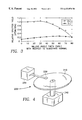
- FIG. 3 is a graph of relative sputter yield verses ion milling angle theta with respect to substrate normal for gold and titanium.
- FIG. 4 depicts an embodiment of the current perpendicular to the plane read head embodied in a data storage and retrieval apparatus in accordance with the present invention.
- FIG. 1 shows a view from the air bearing surface of a current perpendicular to the plane or CPP read head in accordance with the present invention.
- a current perpendicular to the plane or CPP sensor element 30 is formed between lower and upper lead structures 15 & 40 .
- the leads 15 & 40 typically are used both to provide, and to detect changes in, sensing current through the sensor element 30 .
- Insulative material 35 such as alumina, SiO 2 , or other known insulative material, may be formed adjacent the side walls 30 a & 30 b between the leads 15 .
- a photoresist mask 50 is used to pattern the sensor element 30 for ion milling 60 .
- Such a process may be used to defined a pedestal shaped sensor element 30 from deposited thin film layers of sensor material.
- the sensor element may be a giant magnetoresistive multilayer, a spin valve, a spin tunneling junction, or the like, or other known stacked multilayer sensor element.
- the lower lead 15 is used a base to form the sensor element on, an upper portion 15 a of the lower lead 15 is removed by the ion milling 60 during sensor formation. This removed material may redeposit on the side walls 30 a & 30 b of the sensor element 30 as depicted by arrow 25 . In convention CPP devices, this redeposited lead material can cause detrimental current shunting. With the present invention, however, the lower lead 15 is formed so as to inhibit accumulation of removed lower lead material 15 a on side walls 30 a & 30 b of the sensor element 30 .
- the material used to form the upper portion 15 a of the lead, which is exposed to ion milling is selected based upon its sputter yield and its ion beam-to-milling surface angle characteristics.
- a material having a low sputter yield redeposition flux to the side walls is reduced.
- a material having a low value for the ratio between the low angle yield and the high angle yield redeposition accumulation may be minimized.
- a good material to inhibit side wall redeposition accumulation has an increased sputter yield as the milling angle, with respect to the surface milled, increases over the desired range of milling angles.
- FIG. 3 shows empirical data of relative sputter yield verses ion beam-to-substrate angle for gold and titanium.
- the relative sputter yield of gold is higher than that of titanium over the range of zero degrees to near 80 degrees.
- less titanium would sputter from the lead surface and redeposit on the side walls of the sensor when defining the sensor element.
- titanium is a better element for reducing redeposition accumulation because it produces a smaller redeposition flux. It is expected that selecting a material with at least 10 percent lower sputter yield than conventional lead material, at the desired milling angle, would provide a useful reduction in redeposition accumulation on the sensor element side walls.
- the sputter yield for Au decreases from a relative value of one for a zero degree milling angle to less than about 0.2 for an 80 degree milling angle.
- the sputter yield for titanium increases from a relative value of about 0.1 for a zero degree milling angle to about 0.2 for an 80 degree milling angle.
- titanium is a better material to use as lead material 15 a adjacent the sensor element 30 for the purpose of reducing redeposition accumulation on the side walls 30 a & 30 b of the sensor element 30 .
- Titanium and gold were used for comparison purposes as a non-exclusive example, other materials may be used to provide desirable results as discussed further below.
- using the low sputter yield ratio material for etched portion 15 a of the lower lead 15 allows the milling angle ⁇ lead of the lower lead 15 with respect to normal, shown by reference number 65 b, to be selected small to improve etch rate of the lead material, to reduce shadowing, and to reduce reflections. Because the surface 20 a of the lead 15 and the side walls 30 a & 30 b are generally orthogonal, selection of a small milling angle ⁇ lead will produce a corresponding large milling angle ⁇ sidewall with the sensor element side wall 30 a, with respect to sidewall normal, shown by reference number 65 s.
- a low sputter yield ratio material allows the larger milling angle ⁇ sidewall to remove lead material redeposition so as to inhibit accumulation of lead material on the side wall 30 a.
- some embodiments of the present invention may provide a low sputter yield upper portion by forming the entire lead of low sputter yield material, which can minimize fabrication steps.
- Other embodiments may have the lower lead 15 formed by cladding over convention lead material with a low sputter yield ratio material.
- the cladding 20 may be formed of multiple layers of material, each of which may be formed of a different low sputter yield material.
- Cladding conventional lead material is preferred in some embodiments because although low sputter yield ratio materials improve accumulation redeposition, they typically do not have as is low resistivity as conventional lead materials. Low resistance leads are necessary to improve the overall magnetoresistive effect AR/R of the device, particularly in CPP devices. Thus, cladding rather than forming the entire structure from low sputter yield material also allows lead resistance to be minimized.
- the cladding 20 is formed of sufficient thickness to prevent etching of the underlying lead material 10 during the etch process to define the sensor element 30 .
- the cladding 20 may also extend between the sensor element 30 and the underlying low resistivity material 10 in some embodiments. In such embodiments, it is preferable to select a low resistance material for cladding 20 to minimize sensor lead 15 resistance.
- refractory metals are expected to exhibit improved sidewall redeposition accumulation as compared to typical conductive lead materials, such as copper, silver, gold, aluminum, or the like, while also providing adequate electrical conduction.
- conductive lead materials such as copper, silver, gold, aluminum, or the like
- tantalum, titanium, tungsten, molybdenum, zirconium, vanadium, niobium, their alloys, or the like are expected have desirable low sputter yield ratios and sufficiently low resistivity so as to not significantly reduce the magnetoresistive effect of the device.
- the presently preferred embodiments of the invention provide a low resistance lower lead structure to optimize ⁇ R/R while inhibiting redeposition accumulation on the side walls 30 a & 30 b of the sensor element 30 .
- any sidewall redeposition that may occur will have higher resistivity than conventional sidewall deposition.
- preferred embodiments provide reduced shut current in sidewall redeposition as compared to typical lead material sidewall deposition.
- the preferred embodiments of the present invention allow the milling angle with respect to the workpiece to be minimized, processing characteristics are improved.
- the milling angle with respect to the plane of the workpiece may be varied to remove greater amounts of sidewall redeposition.
- the geometry of the element is reduced, however, such a solution becomes impractical. Not only does it impede manufacture rate by reduce vertical milling rate and require more stringent process control, but it also increases shadowing and reflection of the milling beam. Shadowing and reflection limit precise formation of head elements, particularly at small geometries. So, at smaller geometries, increasing the milling angle to reduce sidewall redeposition accumulation is not practical.
- the preferred embodiments of the present invention allow a low milling angle to reduce shadowing and reflection.
- the preferred embodiments allow for precise formation of a small sensor element, which is necessary to improve track width and aerial density.
- the structure and method of the preferred embodiment are expected to produce areal density up to in the range of about 10 Gigabits per inch to 40 Gigabits per inch in typical giant magnetoresistive CPP devices.
- FIG. 4 shows the thin film write head of the present invention embodied in a disk type magnetic data storage and retrieval apparatus 200 .
- the read head of the present invention is located within a merged head assembly 220 which rides above a magnetic storage media 210 , depicted in FIG. 4 as a rotatable hard disk type storage media.
- the hard disk 210 is coupled to a motor 240 to provide rotation of the disk relative to the head assembly 220 .
- An actuating means 230 may be used to position the head assembly 220 above the surface of the media 210 to read and write data in the form of magnetic bits from and to the media 210 .
- the data storage and retrieval apparatus 200 typically has several hard disks 210 and several corresponding head assemblies 220 .
- Embodiments of the present invention may utilize the teaching of U.S. patent application Ser. No. 09/266,678, by Ronald A. Barr, entitled CURRENT PERPENDICULAR TO THE PLANE MAGNETORESISTIVE DEVICE WITH LOW RESISTANCE LEAD, filed on Mar. 11, 1999, issued as U.S. Pat. No. 6,134,089, on Oct. 17, 2000, herein incorporated by reference in its entirety, to improve lead resistance if desired.
Abstract
Description
Claims (1)
Priority Applications (3)
| Application Number | Priority Date | Filing Date | Title |
|---|---|---|---|
| US09/327,209 US6433970B1 (en) | 1999-06-07 | 1999-06-07 | Structure and method for redeposition free thin film CPP read sensor fabrication |
| US10/175,399 US7111382B1 (en) | 1999-06-07 | 2002-06-18 | Methods for fabricating redeposition free thin film CPP read sensors |
| US10/176,874 US6833979B1 (en) | 1999-06-07 | 2002-06-21 | Structure and method for redeposition free thin film CPP read sensor fabrication |
Applications Claiming Priority (1)
| Application Number | Priority Date | Filing Date | Title |
|---|---|---|---|
| US09/327,209 US6433970B1 (en) | 1999-06-07 | 1999-06-07 | Structure and method for redeposition free thin film CPP read sensor fabrication |
Related Child Applications (2)
| Application Number | Title | Priority Date | Filing Date |
|---|---|---|---|
| US10/175,399 Division US7111382B1 (en) | 1999-06-07 | 2002-06-18 | Methods for fabricating redeposition free thin film CPP read sensors |
| US10/176,874 Continuation US6833979B1 (en) | 1999-06-07 | 2002-06-21 | Structure and method for redeposition free thin film CPP read sensor fabrication |
Publications (1)
| Publication Number | Publication Date |
|---|---|
| US6433970B1 true US6433970B1 (en) | 2002-08-13 |
Family
ID=23275595
Family Applications (3)
| Application Number | Title | Priority Date | Filing Date |
|---|---|---|---|
| US09/327,209 Expired - Lifetime US6433970B1 (en) | 1999-06-07 | 1999-06-07 | Structure and method for redeposition free thin film CPP read sensor fabrication |
| US10/175,399 Expired - Lifetime US7111382B1 (en) | 1999-06-07 | 2002-06-18 | Methods for fabricating redeposition free thin film CPP read sensors |
| US10/176,874 Expired - Fee Related US6833979B1 (en) | 1999-06-07 | 2002-06-21 | Structure and method for redeposition free thin film CPP read sensor fabrication |
Family Applications After (2)
| Application Number | Title | Priority Date | Filing Date |
|---|---|---|---|
| US10/175,399 Expired - Lifetime US7111382B1 (en) | 1999-06-07 | 2002-06-18 | Methods for fabricating redeposition free thin film CPP read sensors |
| US10/176,874 Expired - Fee Related US6833979B1 (en) | 1999-06-07 | 2002-06-21 | Structure and method for redeposition free thin film CPP read sensor fabrication |
Country Status (1)
| Country | Link |
|---|---|
| US (3) | US6433970B1 (en) |
Cited By (143)
| Publication number | Priority date | Publication date | Assignee | Title |
|---|---|---|---|---|
| US6833979B1 (en) | 1999-06-07 | 2004-12-21 | Western Digital (Fremont), Inc. | Structure and method for redeposition free thin film CPP read sensor fabrication |
| US20050262686A1 (en) * | 2004-05-28 | 2005-12-01 | Hitachi Global Storage Technologies Netherlands B.V. | Method for making magnetic write head |
| US7296339B1 (en) | 2004-09-08 | 2007-11-20 | Western Digital (Fremont), Llc | Method for manufacturing a perpendicular magnetic recording head |
| US7508627B1 (en) | 2006-03-03 | 2009-03-24 | Western Digital (Fremont), Llc | Method and system for providing perpendicular magnetic recording transducers |
| US7552523B1 (en) | 2005-07-01 | 2009-06-30 | Western Digital (Fremont), Llc | Method for manufacturing a perpendicular magnetic recording transducer |
| US8015692B1 (en) | 2007-11-07 | 2011-09-13 | Western Digital (Fremont), Llc | Method for providing a perpendicular magnetic recording (PMR) head |
| US8141235B1 (en) | 2006-06-09 | 2012-03-27 | Western Digital (Fremont), Llc | Method for manufacturing a perpendicular magnetic recording transducers |
| US8333008B1 (en) | 2005-07-29 | 2012-12-18 | Western Digital (Fremont), Llc | Method for manufacturing a perpendicular magnetic recording transducer |
| US20130113473A1 (en) * | 2011-11-04 | 2013-05-09 | Sae Magnetics (H.K.) | Magnetic sensor with shunting layers and manufacturing method thereof |
| US8486285B2 (en) | 2009-08-20 | 2013-07-16 | Western Digital (Fremont), Llc | Damascene write poles produced via full film plating |
| US8830628B1 (en) | 2009-02-23 | 2014-09-09 | Western Digital (Fremont), Llc | Method and system for providing a perpendicular magnetic recording head |
| US8879207B1 (en) | 2011-12-20 | 2014-11-04 | Western Digital (Fremont), Llc | Method for providing a side shield for a magnetic recording transducer using an air bridge |
| US8883017B1 (en) | 2013-03-12 | 2014-11-11 | Western Digital (Fremont), Llc | Method and system for providing a read transducer having seamless interfaces |
| US8917581B1 (en) | 2013-12-18 | 2014-12-23 | Western Digital Technologies, Inc. | Self-anneal process for a near field transducer and chimney in a hard disk drive assembly |
| US8923102B1 (en) | 2013-07-16 | 2014-12-30 | Western Digital (Fremont), Llc | Optical grating coupling for interferometric waveguides in heat assisted magnetic recording heads |
| US8947985B1 (en) | 2013-07-16 | 2015-02-03 | Western Digital (Fremont), Llc | Heat assisted magnetic recording transducers having a recessed pole |
| US8953422B1 (en) | 2014-06-10 | 2015-02-10 | Western Digital (Fremont), Llc | Near field transducer using dielectric waveguide core with fine ridge feature |
| US8958272B1 (en) | 2014-06-10 | 2015-02-17 | Western Digital (Fremont), Llc | Interfering near field transducer for energy assisted magnetic recording |
| US8970988B1 (en) | 2013-12-31 | 2015-03-03 | Western Digital (Fremont), Llc | Electric gaps and method for making electric gaps for multiple sensor arrays |
| US8971160B1 (en) | 2013-12-19 | 2015-03-03 | Western Digital (Fremont), Llc | Near field transducer with high refractive index pin for heat assisted magnetic recording |
| US8976635B1 (en) | 2014-06-10 | 2015-03-10 | Western Digital (Fremont), Llc | Near field transducer driven by a transverse electric waveguide for energy assisted magnetic recording |
| US8980109B1 (en) | 2012-12-11 | 2015-03-17 | Western Digital (Fremont), Llc | Method for providing a magnetic recording transducer using a combined main pole and side shield CMP for a wraparound shield scheme |
| US8982508B1 (en) | 2011-10-31 | 2015-03-17 | Western Digital (Fremont), Llc | Method for providing a side shield for a magnetic recording transducer |
| US8988825B1 (en) | 2014-02-28 | 2015-03-24 | Western Digital (Fremont, LLC | Method for fabricating a magnetic writer having half-side shields |
| US8984740B1 (en) | 2012-11-30 | 2015-03-24 | Western Digital (Fremont), Llc | Process for providing a magnetic recording transducer having a smooth magnetic seed layer |
| US8988812B1 (en) | 2013-11-27 | 2015-03-24 | Western Digital (Fremont), Llc | Multi-sensor array configuration for a two-dimensional magnetic recording (TDMR) operation |
| US8988835B1 (en) * | 2013-10-14 | 2015-03-24 | International Business Machines Corporation | Contact recording tunnel magnetoresistive sensor with layer of refractory metal |
| US8993217B1 (en) | 2013-04-04 | 2015-03-31 | Western Digital (Fremont), Llc | Double exposure technique for high resolution disk imaging |
| US8995087B1 (en) | 2006-11-29 | 2015-03-31 | Western Digital (Fremont), Llc | Perpendicular magnetic recording write head having a wrap around shield |
| US9001467B1 (en) | 2014-03-05 | 2015-04-07 | Western Digital (Fremont), Llc | Method for fabricating side shields in a magnetic writer |
| US9001628B1 (en) | 2013-12-16 | 2015-04-07 | Western Digital (Fremont), Llc | Assistant waveguides for evaluating main waveguide coupling efficiency and diode laser alignment tolerances for hard disk |
| US8997832B1 (en) | 2010-11-23 | 2015-04-07 | Western Digital (Fremont), Llc | Method of fabricating micrometer scale components |
| US9007879B1 (en) | 2014-06-10 | 2015-04-14 | Western Digital (Fremont), Llc | Interfering near field transducer having a wide metal bar feature for energy assisted magnetic recording |
| US9007725B1 (en) | 2014-10-07 | 2015-04-14 | Western Digital (Fremont), Llc | Sensor with positive coupling between dual ferromagnetic free layer laminates |
| US9007719B1 (en) | 2013-10-23 | 2015-04-14 | Western Digital (Fremont), Llc | Systems and methods for using double mask techniques to achieve very small features |
| US9013836B1 (en) | 2013-04-02 | 2015-04-21 | Western Digital (Fremont), Llc | Method and system for providing an antiferromagnetically coupled return pole |
| US9042057B1 (en) | 2013-01-09 | 2015-05-26 | Western Digital (Fremont), Llc | Methods for providing magnetic storage elements with high magneto-resistance using Heusler alloys |
| US9042052B1 (en) | 2014-06-23 | 2015-05-26 | Western Digital (Fremont), Llc | Magnetic writer having a partially shunted coil |
| US9042058B1 (en) | 2013-10-17 | 2015-05-26 | Western Digital Technologies, Inc. | Shield designed for middle shields in a multiple sensor array |
| US9042051B2 (en) | 2013-08-15 | 2015-05-26 | Western Digital (Fremont), Llc | Gradient write gap for perpendicular magnetic recording writer |
| US9042208B1 (en) | 2013-03-11 | 2015-05-26 | Western Digital Technologies, Inc. | Disk drive measuring fly height by applying a bias voltage to an electrically insulated write component of a head |
| US9053735B1 (en) | 2014-06-20 | 2015-06-09 | Western Digital (Fremont), Llc | Method for fabricating a magnetic writer using a full-film metal planarization |
| US9065043B1 (en) | 2012-06-29 | 2015-06-23 | Western Digital (Fremont), Llc | Tunnel magnetoresistance read head with narrow shield-to-shield spacing |
| US9064507B1 (en) | 2009-07-31 | 2015-06-23 | Western Digital (Fremont), Llc | Magnetic etch-stop layer for magnetoresistive read heads |
| US9064528B1 (en) | 2013-05-17 | 2015-06-23 | Western Digital Technologies, Inc. | Interferometric waveguide usable in shingled heat assisted magnetic recording in the absence of a near-field transducer |
| US9064527B1 (en) | 2013-04-12 | 2015-06-23 | Western Digital (Fremont), Llc | High order tapered waveguide for use in a heat assisted magnetic recording head |
| US9070381B1 (en) | 2013-04-12 | 2015-06-30 | Western Digital (Fremont), Llc | Magnetic recording read transducer having a laminated free layer |
| US9082423B1 (en) | 2013-12-18 | 2015-07-14 | Western Digital (Fremont), Llc | Magnetic recording write transducer having an improved trailing surface profile |
| US9087527B1 (en) | 2014-10-28 | 2015-07-21 | Western Digital (Fremont), Llc | Apparatus and method for middle shield connection in magnetic recording transducers |
| US9087534B1 (en) | 2011-12-20 | 2015-07-21 | Western Digital (Fremont), Llc | Method and system for providing a read transducer having soft and hard magnetic bias structures |
| US9093639B2 (en) | 2012-02-21 | 2015-07-28 | Western Digital (Fremont), Llc | Methods for manufacturing a magnetoresistive structure utilizing heating and cooling |
| US9099118B1 (en) | 2009-05-26 | 2015-08-04 | Western Digital (Fremont), Llc | Dual damascene process for producing a PMR write pole |
| US9104107B1 (en) | 2013-04-03 | 2015-08-11 | Western Digital (Fremont), Llc | DUV photoresist process |
| US9111564B1 (en) | 2013-04-02 | 2015-08-18 | Western Digital (Fremont), Llc | Magnetic recording writer having a main pole with multiple flare angles |
| US9111558B1 (en) | 2014-03-14 | 2015-08-18 | Western Digital (Fremont), Llc | System and method of diffractive focusing of light in a waveguide |
| US9111550B1 (en) | 2014-12-04 | 2015-08-18 | Western Digital (Fremont), Llc | Write transducer having a magnetic buffer layer spaced between a side shield and a write pole by non-magnetic layers |
| US9123362B1 (en) | 2011-03-22 | 2015-09-01 | Western Digital (Fremont), Llc | Methods for assembling an electrically assisted magnetic recording (EAMR) head |
| US9123374B1 (en) | 2015-02-12 | 2015-09-01 | Western Digital (Fremont), Llc | Heat assisted magnetic recording writer having an integrated polarization rotation plate |
| US9123359B1 (en) | 2010-12-22 | 2015-09-01 | Western Digital (Fremont), Llc | Magnetic recording transducer with sputtered antiferromagnetic coupling trilayer between plated ferromagnetic shields and method of fabrication |
| US9123358B1 (en) | 2012-06-11 | 2015-09-01 | Western Digital (Fremont), Llc | Conformal high moment side shield seed layer for perpendicular magnetic recording writer |
| US9135930B1 (en) | 2014-03-06 | 2015-09-15 | Western Digital (Fremont), Llc | Method for fabricating a magnetic write pole using vacuum deposition |
| US9135937B1 (en) | 2014-05-09 | 2015-09-15 | Western Digital (Fremont), Llc | Current modulation on laser diode for energy assisted magnetic recording transducer |
| US9142233B1 (en) | 2014-02-28 | 2015-09-22 | Western Digital (Fremont), Llc | Heat assisted magnetic recording writer having a recessed pole |
| US9147404B1 (en) | 2015-03-31 | 2015-09-29 | Western Digital (Fremont), Llc | Method and system for providing a read transducer having a dual free layer |
| US9147408B1 (en) | 2013-12-19 | 2015-09-29 | Western Digital (Fremont), Llc | Heated AFM layer deposition and cooling process for TMR magnetic recording sensor with high pinning field |
| US9153255B1 (en) | 2014-03-05 | 2015-10-06 | Western Digital (Fremont), Llc | Method for fabricating a magnetic writer having an asymmetric gap and shields |
| US9183854B2 (en) | 2014-02-24 | 2015-11-10 | Western Digital (Fremont), Llc | Method to make interferometric taper waveguide for HAMR light delivery |
| US9190085B1 (en) | 2014-03-12 | 2015-11-17 | Western Digital (Fremont), Llc | Waveguide with reflective grating for localized energy intensity |
| US9190079B1 (en) | 2014-09-22 | 2015-11-17 | Western Digital (Fremont), Llc | Magnetic write pole having engineered radius of curvature and chisel angle profiles |
| US9194692B1 (en) | 2013-12-06 | 2015-11-24 | Western Digital (Fremont), Llc | Systems and methods for using white light interferometry to measure undercut of a bi-layer structure |
| US9202480B2 (en) | 2009-10-14 | 2015-12-01 | Western Digital (Fremont), LLC. | Double patterning hard mask for damascene perpendicular magnetic recording (PMR) writer |
| US9202493B1 (en) | 2014-02-28 | 2015-12-01 | Western Digital (Fremont), Llc | Method of making an ultra-sharp tip mode converter for a HAMR head |
| US9214169B1 (en) | 2014-06-20 | 2015-12-15 | Western Digital (Fremont), Llc | Magnetic recording read transducer having a laminated free layer |
| US9214165B1 (en) | 2014-12-18 | 2015-12-15 | Western Digital (Fremont), Llc | Magnetic writer having a gradient in saturation magnetization of the shields |
| US9214172B2 (en) | 2013-10-23 | 2015-12-15 | Western Digital (Fremont), Llc | Method of manufacturing a magnetic read head |
| US9213322B1 (en) | 2012-08-16 | 2015-12-15 | Western Digital (Fremont), Llc | Methods for providing run to run process control using a dynamic tuner |
| US9230565B1 (en) | 2014-06-24 | 2016-01-05 | Western Digital (Fremont), Llc | Magnetic shield for magnetic recording head |
| US9236560B1 (en) | 2014-12-08 | 2016-01-12 | Western Digital (Fremont), Llc | Spin transfer torque tunneling magnetoresistive device having a laminated free layer with perpendicular magnetic anisotropy |
| US9245543B1 (en) | 2010-06-25 | 2016-01-26 | Western Digital (Fremont), Llc | Method for providing an energy assisted magnetic recording head having a laser integrally mounted to the slider |
| US9245545B1 (en) | 2013-04-12 | 2016-01-26 | Wester Digital (Fremont), Llc | Short yoke length coils for magnetic heads in disk drives |
| US9245562B1 (en) | 2015-03-30 | 2016-01-26 | Western Digital (Fremont), Llc | Magnetic recording writer with a composite main pole |
| US9251813B1 (en) | 2009-04-19 | 2016-02-02 | Western Digital (Fremont), Llc | Method of making a magnetic recording head |
| US9263067B1 (en) | 2013-05-29 | 2016-02-16 | Western Digital (Fremont), Llc | Process for making PMR writer with constant side wall angle |
| US9263071B1 (en) | 2015-03-31 | 2016-02-16 | Western Digital (Fremont), Llc | Flat NFT for heat assisted magnetic recording |
| US9269382B1 (en) | 2012-06-29 | 2016-02-23 | Western Digital (Fremont), Llc | Method and system for providing a read transducer having improved pinning of the pinned layer at higher recording densities |
| US9275657B1 (en) | 2013-08-14 | 2016-03-01 | Western Digital (Fremont), Llc | Process for making PMR writer with non-conformal side gaps |
| US9280990B1 (en) | 2013-12-11 | 2016-03-08 | Western Digital (Fremont), Llc | Method for fabricating a magnetic writer using multiple etches |
| US9287494B1 (en) | 2013-06-28 | 2016-03-15 | Western Digital (Fremont), Llc | Magnetic tunnel junction (MTJ) with a magnesium oxide tunnel barrier |
| US9286919B1 (en) | 2014-12-17 | 2016-03-15 | Western Digital (Fremont), Llc | Magnetic writer having a dual side gap |
| US9305583B1 (en) | 2014-02-18 | 2016-04-05 | Western Digital (Fremont), Llc | Method for fabricating a magnetic writer using multiple etches of damascene materials |
| US9312064B1 (en) | 2015-03-02 | 2016-04-12 | Western Digital (Fremont), Llc | Method to fabricate a magnetic head including ion milling of read gap using dual layer hard mask |
| US9318130B1 (en) | 2013-07-02 | 2016-04-19 | Western Digital (Fremont), Llc | Method to fabricate tunneling magnetic recording heads with extended pinned layer |
| US9336814B1 (en) | 2013-03-12 | 2016-05-10 | Western Digital (Fremont), Llc | Inverse tapered waveguide for use in a heat assisted magnetic recording head |
| US9343086B1 (en) | 2013-09-11 | 2016-05-17 | Western Digital (Fremont), Llc | Magnetic recording write transducer having an improved sidewall angle profile |
| US9343098B1 (en) | 2013-08-23 | 2016-05-17 | Western Digital (Fremont), Llc | Method for providing a heat assisted magnetic recording transducer having protective pads |
| US9343087B1 (en) | 2014-12-21 | 2016-05-17 | Western Digital (Fremont), Llc | Method for fabricating a magnetic writer having half shields |
| US9349394B1 (en) | 2013-10-18 | 2016-05-24 | Western Digital (Fremont), Llc | Method for fabricating a magnetic writer having a gradient side gap |
| US9349392B1 (en) | 2012-05-24 | 2016-05-24 | Western Digital (Fremont), Llc | Methods for improving adhesion on dielectric substrates |
| US9361913B1 (en) | 2013-06-03 | 2016-06-07 | Western Digital (Fremont), Llc | Recording read heads with a multi-layer AFM layer methods and apparatuses |
| US9361914B1 (en) | 2014-06-18 | 2016-06-07 | Western Digital (Fremont), Llc | Magnetic sensor with thin capping layer |
| US9368134B1 (en) | 2010-12-16 | 2016-06-14 | Western Digital (Fremont), Llc | Method and system for providing an antiferromagnetically coupled writer |
| US9384765B1 (en) | 2015-09-24 | 2016-07-05 | Western Digital (Fremont), Llc | Method and system for providing a HAMR writer having improved optical efficiency |
| US9384763B1 (en) | 2015-03-26 | 2016-07-05 | Western Digital (Fremont), Llc | Dual free layer magnetic reader having a rear bias structure including a soft bias layer |
| US9396742B1 (en) | 2012-11-30 | 2016-07-19 | Western Digital (Fremont), Llc | Magnetoresistive sensor for a magnetic storage system read head, and fabrication method thereof |
| US9396743B1 (en) | 2014-02-28 | 2016-07-19 | Western Digital (Fremont), Llc | Systems and methods for controlling soft bias thickness for tunnel magnetoresistance readers |
| US9406331B1 (en) | 2013-06-17 | 2016-08-02 | Western Digital (Fremont), Llc | Method for making ultra-narrow read sensor and read transducer device resulting therefrom |
| US9424866B1 (en) | 2015-09-24 | 2016-08-23 | Western Digital (Fremont), Llc | Heat assisted magnetic recording write apparatus having a dielectric gap |
| US9431039B1 (en) | 2013-05-21 | 2016-08-30 | Western Digital (Fremont), Llc | Multiple sensor array usable in two-dimensional magnetic recording |
| US9431031B1 (en) | 2015-03-24 | 2016-08-30 | Western Digital (Fremont), Llc | System and method for magnetic transducers having multiple sensors and AFC shields |
| US9431047B1 (en) | 2013-05-01 | 2016-08-30 | Western Digital (Fremont), Llc | Method for providing an improved AFM reader shield |
| US9431038B1 (en) | 2015-06-29 | 2016-08-30 | Western Digital (Fremont), Llc | Method for fabricating a magnetic write pole having an improved sidewall angle profile |
| US9431032B1 (en) | 2013-08-14 | 2016-08-30 | Western Digital (Fremont), Llc | Electrical connection arrangement for a multiple sensor array usable in two-dimensional magnetic recording |
| US9437251B1 (en) | 2014-12-22 | 2016-09-06 | Western Digital (Fremont), Llc | Apparatus and method having TDMR reader to reader shunts |
| US9441938B1 (en) | 2013-10-08 | 2016-09-13 | Western Digital (Fremont), Llc | Test structures for measuring near field transducer disc length |
| US9443541B1 (en) | 2015-03-24 | 2016-09-13 | Western Digital (Fremont), Llc | Magnetic writer having a gradient in saturation magnetization of the shields and return pole |
| US9449621B1 (en) | 2015-03-26 | 2016-09-20 | Western Digital (Fremont), Llc | Dual free layer magnetic reader having a rear bias structure having a high aspect ratio |
| US9449625B1 (en) | 2014-12-24 | 2016-09-20 | Western Digital (Fremont), Llc | Heat assisted magnetic recording head having a plurality of diffusion barrier layers |
| US9472216B1 (en) | 2015-09-23 | 2016-10-18 | Western Digital (Fremont), Llc | Differential dual free layer magnetic reader |
| US9484051B1 (en) | 2015-11-09 | 2016-11-01 | The Provost, Fellows, Foundation Scholars and the other members of Board, of the College of the Holy and Undivided Trinity of Queen Elizabeth near Dublin | Method and system for reducing undesirable reflections in a HAMR write apparatus |
| US9508365B1 (en) | 2015-06-24 | 2016-11-29 | Western Digital (Fremont), LLC. | Magnetic reader having a crystal decoupling structure |
| US9508372B1 (en) | 2015-06-03 | 2016-11-29 | Western Digital (Fremont), Llc | Shingle magnetic writer having a low sidewall angle pole |
| US9508363B1 (en) | 2014-06-17 | 2016-11-29 | Western Digital (Fremont), Llc | Method for fabricating a magnetic write pole having a leading edge bevel |
| US9530443B1 (en) | 2015-06-25 | 2016-12-27 | Western Digital (Fremont), Llc | Method for fabricating a magnetic recording device having a high aspect ratio structure |
| US9564150B1 (en) | 2015-11-24 | 2017-02-07 | Western Digital (Fremont), Llc | Magnetic read apparatus having an improved read sensor isolation circuit |
| US9595273B1 (en) | 2015-09-30 | 2017-03-14 | Western Digital (Fremont), Llc | Shingle magnetic writer having nonconformal shields |
| US9646639B2 (en) | 2015-06-26 | 2017-05-09 | Western Digital (Fremont), Llc | Heat assisted magnetic recording writer having integrated polarization rotation waveguides |
| US9666214B1 (en) | 2015-09-23 | 2017-05-30 | Western Digital (Fremont), Llc | Free layer magnetic reader that may have a reduced shield-to-shield spacing |
| US9721595B1 (en) | 2014-12-04 | 2017-08-01 | Western Digital (Fremont), Llc | Method for providing a storage device |
| US9740805B1 (en) | 2015-12-01 | 2017-08-22 | Western Digital (Fremont), Llc | Method and system for detecting hotspots for photolithographically-defined devices |
| US9741366B1 (en) | 2014-12-18 | 2017-08-22 | Western Digital (Fremont), Llc | Method for fabricating a magnetic writer having a gradient in saturation magnetization of the shields |
| US9754611B1 (en) | 2015-11-30 | 2017-09-05 | Western Digital (Fremont), Llc | Magnetic recording write apparatus having a stepped conformal trailing shield |
| US9767831B1 (en) | 2015-12-01 | 2017-09-19 | Western Digital (Fremont), Llc | Magnetic writer having convex trailing surface pole and conformal write gap |
| US9786301B1 (en) | 2014-12-02 | 2017-10-10 | Western Digital (Fremont), Llc | Apparatuses and methods for providing thin shields in a multiple sensor array |
| US9799351B1 (en) | 2015-11-30 | 2017-10-24 | Western Digital (Fremont), Llc | Short yoke length writer having assist coils |
| US9812155B1 (en) | 2015-11-23 | 2017-11-07 | Western Digital (Fremont), Llc | Method and system for fabricating high junction angle read sensors |
| US9842615B1 (en) | 2015-06-26 | 2017-12-12 | Western Digital (Fremont), Llc | Magnetic reader having a nonmagnetic insertion layer for the pinning layer |
| US9858951B1 (en) | 2015-12-01 | 2018-01-02 | Western Digital (Fremont), Llc | Method for providing a multilayer AFM layer in a read sensor |
| US9881638B1 (en) | 2014-12-17 | 2018-01-30 | Western Digital (Fremont), Llc | Method for providing a near-field transducer (NFT) for a heat assisted magnetic recording (HAMR) device |
| US9934811B1 (en) | 2014-03-07 | 2018-04-03 | Western Digital (Fremont), Llc | Methods for controlling stray fields of magnetic features using magneto-elastic anisotropy |
| US9953670B1 (en) | 2015-11-10 | 2018-04-24 | Western Digital (Fremont), Llc | Method and system for providing a HAMR writer including a multi-mode interference device |
| US10037770B1 (en) | 2015-11-12 | 2018-07-31 | Western Digital (Fremont), Llc | Method for providing a magnetic recording write apparatus having a seamless pole |
| US10074387B1 (en) | 2014-12-21 | 2018-09-11 | Western Digital (Fremont), Llc | Method and system for providing a read transducer having symmetric antiferromagnetically coupled shields |
| US10971176B2 (en) | 2019-02-21 | 2021-04-06 | International Business Machines Corporation | Tunnel magnetoresistive sensor with adjacent gap having chromium alloy seed layer and refractory material layer |
Families Citing this family (16)
| Publication number | Priority date | Publication date | Assignee | Title |
|---|---|---|---|---|
| US6700759B1 (en) * | 2000-06-02 | 2004-03-02 | Western Digital (Fremont), Inc. | Narrow track width magnetoresistive sensor and method of making |
| JP3647736B2 (en) * | 2000-09-29 | 2005-05-18 | 株式会社東芝 | Magnetoresistive element, magnetic head, and magnetic reproducing apparatus |
| US7123451B2 (en) * | 2002-09-25 | 2006-10-17 | Tdk Corporation | Thin-film magnetic head for reading magnetic information on a hard disk by utilizing a magnetoresistance effect |
| US7367110B2 (en) * | 2004-09-27 | 2008-05-06 | Hitachi Global Storage Technologies Netherlands B.V. | Method of fabricating a read head having shaped read sensor-biasing layer junctions using partial milling |
| US7419610B2 (en) * | 2005-08-05 | 2008-09-02 | Hitachi Global Storage Technologies Netherlands B.V. | Method of partial depth material removal for fabrication of CPP read sensor |
| DE502005006659D1 (en) * | 2005-09-28 | 2009-04-02 | Siemens Ag | I / O module for an automation device |
| US9013831B2 (en) | 2009-06-22 | 2015-04-21 | Seagate Technology Llc | Write pole fabricated using a carbon hard mask and method of making |
| US8191238B2 (en) * | 2009-06-22 | 2012-06-05 | Seagate Technology Llc | Method for forming a magnetic writer |
| US9786330B1 (en) * | 2016-01-21 | 2017-10-10 | Western Digital Technologies, Inc. | Shield for external welds of hermetically sealed electronics devices |
| US9607635B1 (en) * | 2016-04-22 | 2017-03-28 | International Business Machines Corporation | Current perpendicular-to-plane sensors having hard spacers |
| US9715889B1 (en) | 2016-08-18 | 2017-07-25 | Western Digital (Fremont), Llc | Read sensor having an insulating layer capable of use in two-dimensional magnetic recording |
| US9947348B1 (en) | 2017-02-28 | 2018-04-17 | International Business Machines Corporation | Tunnel magnetoresistive sensor having leads supporting three-dimensional current flow |
| US9997180B1 (en) | 2017-03-22 | 2018-06-12 | International Business Machines Corporation | Hybrid dielectric gap liner and magnetic shield liner |
| US10803889B2 (en) | 2019-02-21 | 2020-10-13 | International Business Machines Corporation | Apparatus with data reader sensors more recessed than servo reader sensor |
| US11074930B1 (en) | 2020-05-11 | 2021-07-27 | International Business Machines Corporation | Read transducer structure having an embedded wear layer between thin and thick shield portions |
| US11114117B1 (en) | 2020-05-20 | 2021-09-07 | International Business Machines Corporation | Process for manufacturing magnetic head having a servo read transducer structure with dielectric gap liner and a data read transducer structure with an embedded wear layer between thin and thick shield portions |
Citations (16)
| Publication number | Priority date | Publication date | Assignee | Title |
|---|---|---|---|---|
| US4914538A (en) * | 1988-08-18 | 1990-04-03 | International Business Machines Corporation | Magnetoresistive read transducer |
| US5268806A (en) * | 1992-01-21 | 1993-12-07 | International Business Machines Corporation | Magnetoresistive transducer having tantalum lead conductors |
| JPH0773418A (en) * | 1993-09-02 | 1995-03-17 | Matsushita Electric Ind Co Ltd | Magneto-resistance effect type thin-film magnetic head |
| US5491600A (en) * | 1994-05-04 | 1996-02-13 | International Business Machines Corporation | Multi-layer conductor leads in a magnetoresistive head |
| US5668688A (en) * | 1996-05-24 | 1997-09-16 | Quantum Peripherals Colorado, Inc. | Current perpendicular-to-the-plane spin valve type magnetoresistive transducer |
| US5680282A (en) * | 1996-10-24 | 1997-10-21 | International Business Machine Corporation | Getter layer lead structure for eliminating resistance increase phonomena and embrittlement and method for making the same |
| US5828232A (en) * | 1995-11-16 | 1998-10-27 | Texas Instruments Incorporated | Circuit to reduce current and voltage spikes when switching inductive loads |
| JPH1139611A (en) * | 1997-07-11 | 1999-02-12 | Hitachi Ltd | Magneto-resistive head and magnetic memory device using the same |
| US5883764A (en) * | 1997-10-03 | 1999-03-16 | International Business Machines Corporation | Magnetoresistive sensor having multi-layered refractory metal conductor leads |
| US5901018A (en) * | 1997-10-24 | 1999-05-04 | International Business Machines Corporation | Magnetic tunnel junction magnetoresistive read head with sensing layer as rear flux guide |
| US6002553A (en) * | 1994-02-28 | 1999-12-14 | The United States Of America As Represented By The United States Department Of Energy | Giant magnetoresistive sensor |
| US6023395A (en) * | 1998-05-29 | 2000-02-08 | International Business Machines Corporation | Magnetic tunnel junction magnetoresistive sensor with in-stack biasing |
| US6114719A (en) * | 1998-05-29 | 2000-09-05 | International Business Machines Corporation | Magnetic tunnel junction memory cell with in-stack biasing of the free ferromagnetic layer and memory array using the cell |
| US6118638A (en) * | 1998-11-02 | 2000-09-12 | Read-Rite Corporation | CPP magnetoresistive device and method for making same |
| US6134089A (en) * | 1999-03-11 | 2000-10-17 | Read-Rite Corporation | Current perpendicular to plane magnetoresistive device with low resistance lead |
| US6249407B1 (en) * | 1999-02-05 | 2001-06-19 | Fujitsu Limited | Magnetoresistive device having a tantalum layer connected to a shielding layer via a layer of a body-centered cubic structure |
Family Cites Families (10)
| Publication number | Priority date | Publication date | Assignee | Title |
|---|---|---|---|---|
| US3666665A (en) * | 1970-12-14 | 1972-05-30 | Ibm | Composition of ferroelectric matter |
| US4230750A (en) * | 1979-08-15 | 1980-10-28 | Eutectic Corporation | Metallo-thermic powder |
| JPS6184572A (en) | 1984-10-02 | 1986-04-30 | Tdk Corp | Magnetic sensor |
| JPS6395983A (en) * | 1986-10-14 | 1988-04-26 | Mitsubishi Kasei Corp | Optical recording medium |
| JP2746798B2 (en) * | 1992-07-29 | 1998-05-06 | 京セラ株式会社 | Wiring board |
| US5946167A (en) * | 1996-03-15 | 1999-08-31 | Kabushiki Kaisha Toshiba | Magnetoresistive sensor having lead and/or bias layer structure contributing to a narrow gap |
| JPH10208217A (en) | 1997-01-24 | 1998-08-07 | Fuji Elelctrochem Co Ltd | Production of thin film magnetic head |
| US5920980A (en) * | 1997-03-05 | 1999-07-13 | Headway Technologies, Inc. | Method of making a soft adjacent layer (SAL) magnetoresistive (MR) sensor element with electrically insulated soft adjacent layer (SAL) |
| US5959811A (en) | 1998-01-13 | 1999-09-28 | Read-Rite Corporation | Magnetoresistive transducer with four-lead contact |
| US6433970B1 (en) | 1999-06-07 | 2002-08-13 | Read-Rite Corporation | Structure and method for redeposition free thin film CPP read sensor fabrication |
-
1999
- 1999-06-07 US US09/327,209 patent/US6433970B1/en not_active Expired - Lifetime
-
2002
- 2002-06-18 US US10/175,399 patent/US7111382B1/en not_active Expired - Lifetime
- 2002-06-21 US US10/176,874 patent/US6833979B1/en not_active Expired - Fee Related
Patent Citations (16)
| Publication number | Priority date | Publication date | Assignee | Title |
|---|---|---|---|---|
| US4914538A (en) * | 1988-08-18 | 1990-04-03 | International Business Machines Corporation | Magnetoresistive read transducer |
| US5268806A (en) * | 1992-01-21 | 1993-12-07 | International Business Machines Corporation | Magnetoresistive transducer having tantalum lead conductors |
| JPH0773418A (en) * | 1993-09-02 | 1995-03-17 | Matsushita Electric Ind Co Ltd | Magneto-resistance effect type thin-film magnetic head |
| US6002553A (en) * | 1994-02-28 | 1999-12-14 | The United States Of America As Represented By The United States Department Of Energy | Giant magnetoresistive sensor |
| US5491600A (en) * | 1994-05-04 | 1996-02-13 | International Business Machines Corporation | Multi-layer conductor leads in a magnetoresistive head |
| US5828232A (en) * | 1995-11-16 | 1998-10-27 | Texas Instruments Incorporated | Circuit to reduce current and voltage spikes when switching inductive loads |
| US5668688A (en) * | 1996-05-24 | 1997-09-16 | Quantum Peripherals Colorado, Inc. | Current perpendicular-to-the-plane spin valve type magnetoresistive transducer |
| US5680282A (en) * | 1996-10-24 | 1997-10-21 | International Business Machine Corporation | Getter layer lead structure for eliminating resistance increase phonomena and embrittlement and method for making the same |
| JPH1139611A (en) * | 1997-07-11 | 1999-02-12 | Hitachi Ltd | Magneto-resistive head and magnetic memory device using the same |
| US5883764A (en) * | 1997-10-03 | 1999-03-16 | International Business Machines Corporation | Magnetoresistive sensor having multi-layered refractory metal conductor leads |
| US5901018A (en) * | 1997-10-24 | 1999-05-04 | International Business Machines Corporation | Magnetic tunnel junction magnetoresistive read head with sensing layer as rear flux guide |
| US6023395A (en) * | 1998-05-29 | 2000-02-08 | International Business Machines Corporation | Magnetic tunnel junction magnetoresistive sensor with in-stack biasing |
| US6114719A (en) * | 1998-05-29 | 2000-09-05 | International Business Machines Corporation | Magnetic tunnel junction memory cell with in-stack biasing of the free ferromagnetic layer and memory array using the cell |
| US6118638A (en) * | 1998-11-02 | 2000-09-12 | Read-Rite Corporation | CPP magnetoresistive device and method for making same |
| US6249407B1 (en) * | 1999-02-05 | 2001-06-19 | Fujitsu Limited | Magnetoresistive device having a tantalum layer connected to a shielding layer via a layer of a body-centered cubic structure |
| US6134089A (en) * | 1999-03-11 | 2000-10-17 | Read-Rite Corporation | Current perpendicular to plane magnetoresistive device with low resistance lead |
Non-Patent Citations (4)
| Title |
|---|
| Cantagrel, Michel, "Considerations on High Resolution Patterns Engraved by Ion Etching," IEEE Transactions on Electron Devices, vol. ED-22, No. 7, Jul. 1995, pp. 483-486. |
| Lee, Robert E., "Microfabrication by ion-beam etching," J. Vac. Sci. Tchnol., 16(2), Mar./Apr. 1979, pp. 164-170. |
| Melliar-Smith, C.M., "Ion etching for pattern delineation," J. Vac. Sci. Technol., 13(5), Sep./Oct. 1976, 1008-1022. |
| U.S. patent application Publication No. 2001/0005301 A1 filed Jun. 28, 2001, to Komuro et al.* * |
Cited By (166)
| Publication number | Priority date | Publication date | Assignee | Title |
|---|---|---|---|---|
| US7111382B1 (en) | 1999-06-07 | 2006-09-26 | Western Digital (Fremont), Inc. | Methods for fabricating redeposition free thin film CPP read sensors |
| US6833979B1 (en) | 1999-06-07 | 2004-12-21 | Western Digital (Fremont), Inc. | Structure and method for redeposition free thin film CPP read sensor fabrication |
| US7480983B2 (en) * | 2004-05-28 | 2009-01-27 | Hitachi Global Storage Technologies Netherlands B.V. | Method for making magnetic write head |
| US20050262686A1 (en) * | 2004-05-28 | 2005-12-01 | Hitachi Global Storage Technologies Netherlands B.V. | Method for making magnetic write head |
| US8149536B1 (en) | 2004-09-08 | 2012-04-03 | Western Digital (Fremont), Llc | Perpendicular magnetic recording head having a pole tip formed with a CMP uniformity structure |
| US7296339B1 (en) | 2004-09-08 | 2007-11-20 | Western Digital (Fremont), Llc | Method for manufacturing a perpendicular magnetic recording head |
| US7552523B1 (en) | 2005-07-01 | 2009-06-30 | Western Digital (Fremont), Llc | Method for manufacturing a perpendicular magnetic recording transducer |
| US8333008B1 (en) | 2005-07-29 | 2012-12-18 | Western Digital (Fremont), Llc | Method for manufacturing a perpendicular magnetic recording transducer |
| US7508627B1 (en) | 2006-03-03 | 2009-03-24 | Western Digital (Fremont), Llc | Method and system for providing perpendicular magnetic recording transducers |
| US8141235B1 (en) | 2006-06-09 | 2012-03-27 | Western Digital (Fremont), Llc | Method for manufacturing a perpendicular magnetic recording transducers |
| US8861134B1 (en) | 2006-06-09 | 2014-10-14 | Western Digital (Fremont), Llc | Method and system for providing perpendicular magnetic recording transducers utilizing a damascene approach |
| US8468682B1 (en) | 2006-06-09 | 2013-06-25 | Western Digital (Fremont), Llc | Method for manufacturing perpendicular magnetic recording transducers |
| US8995087B1 (en) | 2006-11-29 | 2015-03-31 | Western Digital (Fremont), Llc | Perpendicular magnetic recording write head having a wrap around shield |
| US8015692B1 (en) | 2007-11-07 | 2011-09-13 | Western Digital (Fremont), Llc | Method for providing a perpendicular magnetic recording (PMR) head |
| US8830628B1 (en) | 2009-02-23 | 2014-09-09 | Western Digital (Fremont), Llc | Method and system for providing a perpendicular magnetic recording head |
| US9251813B1 (en) | 2009-04-19 | 2016-02-02 | Western Digital (Fremont), Llc | Method of making a magnetic recording head |
| US9099118B1 (en) | 2009-05-26 | 2015-08-04 | Western Digital (Fremont), Llc | Dual damascene process for producing a PMR write pole |
| US9064507B1 (en) | 2009-07-31 | 2015-06-23 | Western Digital (Fremont), Llc | Magnetic etch-stop layer for magnetoresistive read heads |
| US8486285B2 (en) | 2009-08-20 | 2013-07-16 | Western Digital (Fremont), Llc | Damascene write poles produced via full film plating |
| US9202480B2 (en) | 2009-10-14 | 2015-12-01 | Western Digital (Fremont), LLC. | Double patterning hard mask for damascene perpendicular magnetic recording (PMR) writer |
| US9245543B1 (en) | 2010-06-25 | 2016-01-26 | Western Digital (Fremont), Llc | Method for providing an energy assisted magnetic recording head having a laser integrally mounted to the slider |
| US9159345B1 (en) | 2010-11-23 | 2015-10-13 | Western Digital (Fremont), Llc | Micrometer scale components |
| US9672847B2 (en) | 2010-11-23 | 2017-06-06 | Western Digital (Fremont), Llc | Micrometer scale components |
| US8997832B1 (en) | 2010-11-23 | 2015-04-07 | Western Digital (Fremont), Llc | Method of fabricating micrometer scale components |
| US9368134B1 (en) | 2010-12-16 | 2016-06-14 | Western Digital (Fremont), Llc | Method and system for providing an antiferromagnetically coupled writer |
| US9123359B1 (en) | 2010-12-22 | 2015-09-01 | Western Digital (Fremont), Llc | Magnetic recording transducer with sputtered antiferromagnetic coupling trilayer between plated ferromagnetic shields and method of fabrication |
| US9123362B1 (en) | 2011-03-22 | 2015-09-01 | Western Digital (Fremont), Llc | Methods for assembling an electrically assisted magnetic recording (EAMR) head |
| US8982508B1 (en) | 2011-10-31 | 2015-03-17 | Western Digital (Fremont), Llc | Method for providing a side shield for a magnetic recording transducer |
| US20130113473A1 (en) * | 2011-11-04 | 2013-05-09 | Sae Magnetics (H.K.) | Magnetic sensor with shunting layers and manufacturing method thereof |
| US9087534B1 (en) | 2011-12-20 | 2015-07-21 | Western Digital (Fremont), Llc | Method and system for providing a read transducer having soft and hard magnetic bias structures |
| US8879207B1 (en) | 2011-12-20 | 2014-11-04 | Western Digital (Fremont), Llc | Method for providing a side shield for a magnetic recording transducer using an air bridge |
| US9093639B2 (en) | 2012-02-21 | 2015-07-28 | Western Digital (Fremont), Llc | Methods for manufacturing a magnetoresistive structure utilizing heating and cooling |
| US9940950B2 (en) | 2012-05-24 | 2018-04-10 | Western Digital (Fremont), Llc | Methods for improving adhesion on dielectric substrates |
| US9349392B1 (en) | 2012-05-24 | 2016-05-24 | Western Digital (Fremont), Llc | Methods for improving adhesion on dielectric substrates |
| US9123358B1 (en) | 2012-06-11 | 2015-09-01 | Western Digital (Fremont), Llc | Conformal high moment side shield seed layer for perpendicular magnetic recording writer |
| US9412400B2 (en) | 2012-06-29 | 2016-08-09 | Western Digital (Fremont), Llc | Tunnel magnetoresistance read head with narrow shield-to-shield spacing |
| US9065043B1 (en) | 2012-06-29 | 2015-06-23 | Western Digital (Fremont), Llc | Tunnel magnetoresistance read head with narrow shield-to-shield spacing |
| US9269382B1 (en) | 2012-06-29 | 2016-02-23 | Western Digital (Fremont), Llc | Method and system for providing a read transducer having improved pinning of the pinned layer at higher recording densities |
| US9213322B1 (en) | 2012-08-16 | 2015-12-15 | Western Digital (Fremont), Llc | Methods for providing run to run process control using a dynamic tuner |
| US9396742B1 (en) | 2012-11-30 | 2016-07-19 | Western Digital (Fremont), Llc | Magnetoresistive sensor for a magnetic storage system read head, and fabrication method thereof |
| US8984740B1 (en) | 2012-11-30 | 2015-03-24 | Western Digital (Fremont), Llc | Process for providing a magnetic recording transducer having a smooth magnetic seed layer |
| US8980109B1 (en) | 2012-12-11 | 2015-03-17 | Western Digital (Fremont), Llc | Method for providing a magnetic recording transducer using a combined main pole and side shield CMP for a wraparound shield scheme |
| US9042057B1 (en) | 2013-01-09 | 2015-05-26 | Western Digital (Fremont), Llc | Methods for providing magnetic storage elements with high magneto-resistance using Heusler alloys |
| US9042208B1 (en) | 2013-03-11 | 2015-05-26 | Western Digital Technologies, Inc. | Disk drive measuring fly height by applying a bias voltage to an electrically insulated write component of a head |
| US9336814B1 (en) | 2013-03-12 | 2016-05-10 | Western Digital (Fremont), Llc | Inverse tapered waveguide for use in a heat assisted magnetic recording head |
| US8883017B1 (en) | 2013-03-12 | 2014-11-11 | Western Digital (Fremont), Llc | Method and system for providing a read transducer having seamless interfaces |
| US9013836B1 (en) | 2013-04-02 | 2015-04-21 | Western Digital (Fremont), Llc | Method and system for providing an antiferromagnetically coupled return pole |
| US9111564B1 (en) | 2013-04-02 | 2015-08-18 | Western Digital (Fremont), Llc | Magnetic recording writer having a main pole with multiple flare angles |
| US9104107B1 (en) | 2013-04-03 | 2015-08-11 | Western Digital (Fremont), Llc | DUV photoresist process |
| US8993217B1 (en) | 2013-04-04 | 2015-03-31 | Western Digital (Fremont), Llc | Double exposure technique for high resolution disk imaging |
| US9064527B1 (en) | 2013-04-12 | 2015-06-23 | Western Digital (Fremont), Llc | High order tapered waveguide for use in a heat assisted magnetic recording head |
| US9070381B1 (en) | 2013-04-12 | 2015-06-30 | Western Digital (Fremont), Llc | Magnetic recording read transducer having a laminated free layer |
| US9245545B1 (en) | 2013-04-12 | 2016-01-26 | Wester Digital (Fremont), Llc | Short yoke length coils for magnetic heads in disk drives |
| US9431047B1 (en) | 2013-05-01 | 2016-08-30 | Western Digital (Fremont), Llc | Method for providing an improved AFM reader shield |
| US9064528B1 (en) | 2013-05-17 | 2015-06-23 | Western Digital Technologies, Inc. | Interferometric waveguide usable in shingled heat assisted magnetic recording in the absence of a near-field transducer |
| US9431039B1 (en) | 2013-05-21 | 2016-08-30 | Western Digital (Fremont), Llc | Multiple sensor array usable in two-dimensional magnetic recording |
| US9263067B1 (en) | 2013-05-29 | 2016-02-16 | Western Digital (Fremont), Llc | Process for making PMR writer with constant side wall angle |
| US9361913B1 (en) | 2013-06-03 | 2016-06-07 | Western Digital (Fremont), Llc | Recording read heads with a multi-layer AFM layer methods and apparatuses |
| US9406331B1 (en) | 2013-06-17 | 2016-08-02 | Western Digital (Fremont), Llc | Method for making ultra-narrow read sensor and read transducer device resulting therefrom |
| US9287494B1 (en) | 2013-06-28 | 2016-03-15 | Western Digital (Fremont), Llc | Magnetic tunnel junction (MTJ) with a magnesium oxide tunnel barrier |
| US9318130B1 (en) | 2013-07-02 | 2016-04-19 | Western Digital (Fremont), Llc | Method to fabricate tunneling magnetic recording heads with extended pinned layer |
| US8947985B1 (en) | 2013-07-16 | 2015-02-03 | Western Digital (Fremont), Llc | Heat assisted magnetic recording transducers having a recessed pole |
| US8923102B1 (en) | 2013-07-16 | 2014-12-30 | Western Digital (Fremont), Llc | Optical grating coupling for interferometric waveguides in heat assisted magnetic recording heads |
| US9431032B1 (en) | 2013-08-14 | 2016-08-30 | Western Digital (Fremont), Llc | Electrical connection arrangement for a multiple sensor array usable in two-dimensional magnetic recording |
| US9275657B1 (en) | 2013-08-14 | 2016-03-01 | Western Digital (Fremont), Llc | Process for making PMR writer with non-conformal side gaps |
| US9042051B2 (en) | 2013-08-15 | 2015-05-26 | Western Digital (Fremont), Llc | Gradient write gap for perpendicular magnetic recording writer |
| US9343098B1 (en) | 2013-08-23 | 2016-05-17 | Western Digital (Fremont), Llc | Method for providing a heat assisted magnetic recording transducer having protective pads |
| US9343086B1 (en) | 2013-09-11 | 2016-05-17 | Western Digital (Fremont), Llc | Magnetic recording write transducer having an improved sidewall angle profile |
| US9441938B1 (en) | 2013-10-08 | 2016-09-13 | Western Digital (Fremont), Llc | Test structures for measuring near field transducer disc length |
| US9293158B2 (en) | 2013-10-14 | 2016-03-22 | International Business Machines Corporation | Apparatus having tunnel magnetoresistive sensor for contact recording |
| US8988835B1 (en) * | 2013-10-14 | 2015-03-24 | International Business Machines Corporation | Contact recording tunnel magnetoresistive sensor with layer of refractory metal |
| US9042058B1 (en) | 2013-10-17 | 2015-05-26 | Western Digital Technologies, Inc. | Shield designed for middle shields in a multiple sensor array |
| US9349394B1 (en) | 2013-10-18 | 2016-05-24 | Western Digital (Fremont), Llc | Method for fabricating a magnetic writer having a gradient side gap |
| US9214172B2 (en) | 2013-10-23 | 2015-12-15 | Western Digital (Fremont), Llc | Method of manufacturing a magnetic read head |
| US9007719B1 (en) | 2013-10-23 | 2015-04-14 | Western Digital (Fremont), Llc | Systems and methods for using double mask techniques to achieve very small features |
| US9830936B2 (en) | 2013-10-23 | 2017-11-28 | Western Digital (Fremont), Llc | Magnetic read head with antiferromagentic layer |
| US8988812B1 (en) | 2013-11-27 | 2015-03-24 | Western Digital (Fremont), Llc | Multi-sensor array configuration for a two-dimensional magnetic recording (TDMR) operation |
| US9194692B1 (en) | 2013-12-06 | 2015-11-24 | Western Digital (Fremont), Llc | Systems and methods for using white light interferometry to measure undercut of a bi-layer structure |
| US9280990B1 (en) | 2013-12-11 | 2016-03-08 | Western Digital (Fremont), Llc | Method for fabricating a magnetic writer using multiple etches |
| US9001628B1 (en) | 2013-12-16 | 2015-04-07 | Western Digital (Fremont), Llc | Assistant waveguides for evaluating main waveguide coupling efficiency and diode laser alignment tolerances for hard disk |
| US9082423B1 (en) | 2013-12-18 | 2015-07-14 | Western Digital (Fremont), Llc | Magnetic recording write transducer having an improved trailing surface profile |
| US8917581B1 (en) | 2013-12-18 | 2014-12-23 | Western Digital Technologies, Inc. | Self-anneal process for a near field transducer and chimney in a hard disk drive assembly |
| US8971160B1 (en) | 2013-12-19 | 2015-03-03 | Western Digital (Fremont), Llc | Near field transducer with high refractive index pin for heat assisted magnetic recording |
| US9147408B1 (en) | 2013-12-19 | 2015-09-29 | Western Digital (Fremont), Llc | Heated AFM layer deposition and cooling process for TMR magnetic recording sensor with high pinning field |
| US8970988B1 (en) | 2013-12-31 | 2015-03-03 | Western Digital (Fremont), Llc | Electric gaps and method for making electric gaps for multiple sensor arrays |
| US9305583B1 (en) | 2014-02-18 | 2016-04-05 | Western Digital (Fremont), Llc | Method for fabricating a magnetic writer using multiple etches of damascene materials |
| US9183854B2 (en) | 2014-02-24 | 2015-11-10 | Western Digital (Fremont), Llc | Method to make interferometric taper waveguide for HAMR light delivery |
| US9142233B1 (en) | 2014-02-28 | 2015-09-22 | Western Digital (Fremont), Llc | Heat assisted magnetic recording writer having a recessed pole |
| US8988825B1 (en) | 2014-02-28 | 2015-03-24 | Western Digital (Fremont, LLC | Method for fabricating a magnetic writer having half-side shields |
| US9202493B1 (en) | 2014-02-28 | 2015-12-01 | Western Digital (Fremont), Llc | Method of making an ultra-sharp tip mode converter for a HAMR head |
| US9396743B1 (en) | 2014-02-28 | 2016-07-19 | Western Digital (Fremont), Llc | Systems and methods for controlling soft bias thickness for tunnel magnetoresistance readers |
| US9349393B2 (en) | 2014-03-05 | 2016-05-24 | Western Digital (Fremont), Llc | Magnetic writer having an asymmetric gap and shields |
| US9001467B1 (en) | 2014-03-05 | 2015-04-07 | Western Digital (Fremont), Llc | Method for fabricating side shields in a magnetic writer |
| US9153255B1 (en) | 2014-03-05 | 2015-10-06 | Western Digital (Fremont), Llc | Method for fabricating a magnetic writer having an asymmetric gap and shields |
| US9135930B1 (en) | 2014-03-06 | 2015-09-15 | Western Digital (Fremont), Llc | Method for fabricating a magnetic write pole using vacuum deposition |
| US9934811B1 (en) | 2014-03-07 | 2018-04-03 | Western Digital (Fremont), Llc | Methods for controlling stray fields of magnetic features using magneto-elastic anisotropy |
| US9190085B1 (en) | 2014-03-12 | 2015-11-17 | Western Digital (Fremont), Llc | Waveguide with reflective grating for localized energy intensity |
| US9495984B2 (en) | 2014-03-12 | 2016-11-15 | Western Digital (Fremont), Llc | Waveguide with reflective grating for localized energy intensity |
| US9111558B1 (en) | 2014-03-14 | 2015-08-18 | Western Digital (Fremont), Llc | System and method of diffractive focusing of light in a waveguide |
| US9135937B1 (en) | 2014-05-09 | 2015-09-15 | Western Digital (Fremont), Llc | Current modulation on laser diode for energy assisted magnetic recording transducer |
| US8976635B1 (en) | 2014-06-10 | 2015-03-10 | Western Digital (Fremont), Llc | Near field transducer driven by a transverse electric waveguide for energy assisted magnetic recording |
| US8953422B1 (en) | 2014-06-10 | 2015-02-10 | Western Digital (Fremont), Llc | Near field transducer using dielectric waveguide core with fine ridge feature |
| US8958272B1 (en) | 2014-06-10 | 2015-02-17 | Western Digital (Fremont), Llc | Interfering near field transducer for energy assisted magnetic recording |
| US9159346B1 (en) | 2014-06-10 | 2015-10-13 | Western Digital (Fremont), Llc | Near field transducer using dielectric waveguide core with fine ridge feature |
| US9007879B1 (en) | 2014-06-10 | 2015-04-14 | Western Digital (Fremont), Llc | Interfering near field transducer having a wide metal bar feature for energy assisted magnetic recording |
| US9311952B2 (en) | 2014-06-10 | 2016-04-12 | Western Digital (Fremont), Llc | Interfering near field transducer for energy assisted magnetic recording |
| US9508363B1 (en) | 2014-06-17 | 2016-11-29 | Western Digital (Fremont), Llc | Method for fabricating a magnetic write pole having a leading edge bevel |
| US9361914B1 (en) | 2014-06-18 | 2016-06-07 | Western Digital (Fremont), Llc | Magnetic sensor with thin capping layer |
| US9053735B1 (en) | 2014-06-20 | 2015-06-09 | Western Digital (Fremont), Llc | Method for fabricating a magnetic writer using a full-film metal planarization |
| US9214169B1 (en) | 2014-06-20 | 2015-12-15 | Western Digital (Fremont), Llc | Magnetic recording read transducer having a laminated free layer |
| US9042052B1 (en) | 2014-06-23 | 2015-05-26 | Western Digital (Fremont), Llc | Magnetic writer having a partially shunted coil |
| US9230565B1 (en) | 2014-06-24 | 2016-01-05 | Western Digital (Fremont), Llc | Magnetic shield for magnetic recording head |
| US9190079B1 (en) | 2014-09-22 | 2015-11-17 | Western Digital (Fremont), Llc | Magnetic write pole having engineered radius of curvature and chisel angle profiles |
| US9007725B1 (en) | 2014-10-07 | 2015-04-14 | Western Digital (Fremont), Llc | Sensor with positive coupling between dual ferromagnetic free layer laminates |
| US9087527B1 (en) | 2014-10-28 | 2015-07-21 | Western Digital (Fremont), Llc | Apparatus and method for middle shield connection in magnetic recording transducers |
| US9786301B1 (en) | 2014-12-02 | 2017-10-10 | Western Digital (Fremont), Llc | Apparatuses and methods for providing thin shields in a multiple sensor array |
| US9721595B1 (en) | 2014-12-04 | 2017-08-01 | Western Digital (Fremont), Llc | Method for providing a storage device |
| US9111550B1 (en) | 2014-12-04 | 2015-08-18 | Western Digital (Fremont), Llc | Write transducer having a magnetic buffer layer spaced between a side shield and a write pole by non-magnetic layers |
| US9236560B1 (en) | 2014-12-08 | 2016-01-12 | Western Digital (Fremont), Llc | Spin transfer torque tunneling magnetoresistive device having a laminated free layer with perpendicular magnetic anisotropy |
| US9705072B2 (en) | 2014-12-08 | 2017-07-11 | Western Digital (Fremont), Llc | Spin transfer torque tunneling magnetoresistive device having a laminated free layer with perpendicular magnetic anisotropy |
| US10553241B2 (en) | 2014-12-17 | 2020-02-04 | Western Digital Technologies, Inc. | Near-field transducer (NFT) for a heat assisted magnetic recording (HAMR) device |
| US9286919B1 (en) | 2014-12-17 | 2016-03-15 | Western Digital (Fremont), Llc | Magnetic writer having a dual side gap |
| US9881638B1 (en) | 2014-12-17 | 2018-01-30 | Western Digital (Fremont), Llc | Method for providing a near-field transducer (NFT) for a heat assisted magnetic recording (HAMR) device |
| US9741366B1 (en) | 2014-12-18 | 2017-08-22 | Western Digital (Fremont), Llc | Method for fabricating a magnetic writer having a gradient in saturation magnetization of the shields |
| US9214165B1 (en) | 2014-12-18 | 2015-12-15 | Western Digital (Fremont), Llc | Magnetic writer having a gradient in saturation magnetization of the shields |
| US10074387B1 (en) | 2014-12-21 | 2018-09-11 | Western Digital (Fremont), Llc | Method and system for providing a read transducer having symmetric antiferromagnetically coupled shields |
| US9343087B1 (en) | 2014-12-21 | 2016-05-17 | Western Digital (Fremont), Llc | Method for fabricating a magnetic writer having half shields |
| US9437251B1 (en) | 2014-12-22 | 2016-09-06 | Western Digital (Fremont), Llc | Apparatus and method having TDMR reader to reader shunts |
| US9449625B1 (en) | 2014-12-24 | 2016-09-20 | Western Digital (Fremont), Llc | Heat assisted magnetic recording head having a plurality of diffusion barrier layers |
| US9123374B1 (en) | 2015-02-12 | 2015-09-01 | Western Digital (Fremont), Llc | Heat assisted magnetic recording writer having an integrated polarization rotation plate |
| US9312064B1 (en) | 2015-03-02 | 2016-04-12 | Western Digital (Fremont), Llc | Method to fabricate a magnetic head including ion milling of read gap using dual layer hard mask |
| US9443541B1 (en) | 2015-03-24 | 2016-09-13 | Western Digital (Fremont), Llc | Magnetic writer having a gradient in saturation magnetization of the shields and return pole |
| US9431031B1 (en) | 2015-03-24 | 2016-08-30 | Western Digital (Fremont), Llc | System and method for magnetic transducers having multiple sensors and AFC shields |
| US9922672B1 (en) | 2015-03-26 | 2018-03-20 | Western Digital (Fremont), Llc | Dual free layer magnetic reader having a rear bias structure having a high aspect ratio |
| US9384763B1 (en) | 2015-03-26 | 2016-07-05 | Western Digital (Fremont), Llc | Dual free layer magnetic reader having a rear bias structure including a soft bias layer |
| US9449621B1 (en) | 2015-03-26 | 2016-09-20 | Western Digital (Fremont), Llc | Dual free layer magnetic reader having a rear bias structure having a high aspect ratio |
| US9245562B1 (en) | 2015-03-30 | 2016-01-26 | Western Digital (Fremont), Llc | Magnetic recording writer with a composite main pole |
| US9263071B1 (en) | 2015-03-31 | 2016-02-16 | Western Digital (Fremont), Llc | Flat NFT for heat assisted magnetic recording |
| US9147404B1 (en) | 2015-03-31 | 2015-09-29 | Western Digital (Fremont), Llc | Method and system for providing a read transducer having a dual free layer |
| US9508372B1 (en) | 2015-06-03 | 2016-11-29 | Western Digital (Fremont), Llc | Shingle magnetic writer having a low sidewall angle pole |
| US9508365B1 (en) | 2015-06-24 | 2016-11-29 | Western Digital (Fremont), LLC. | Magnetic reader having a crystal decoupling structure |
| US9530443B1 (en) | 2015-06-25 | 2016-12-27 | Western Digital (Fremont), Llc | Method for fabricating a magnetic recording device having a high aspect ratio structure |
| US9646639B2 (en) | 2015-06-26 | 2017-05-09 | Western Digital (Fremont), Llc | Heat assisted magnetic recording writer having integrated polarization rotation waveguides |
| US9842615B1 (en) | 2015-06-26 | 2017-12-12 | Western Digital (Fremont), Llc | Magnetic reader having a nonmagnetic insertion layer for the pinning layer |
| US10242700B2 (en) | 2015-06-26 | 2019-03-26 | Western Digital (Fremont), Llc | Magnetic reader having a nonmagnetic insertion layer for the pinning layer |
| US10037773B2 (en) | 2015-06-26 | 2018-07-31 | Western Digital (Fremont), Llc | Heat assisted magnetic recording writer having integrated polarization rotation waveguides |
| US9431038B1 (en) | 2015-06-29 | 2016-08-30 | Western Digital (Fremont), Llc | Method for fabricating a magnetic write pole having an improved sidewall angle profile |
| US9472216B1 (en) | 2015-09-23 | 2016-10-18 | Western Digital (Fremont), Llc | Differential dual free layer magnetic reader |
| US9666214B1 (en) | 2015-09-23 | 2017-05-30 | Western Digital (Fremont), Llc | Free layer magnetic reader that may have a reduced shield-to-shield spacing |
| US9424866B1 (en) | 2015-09-24 | 2016-08-23 | Western Digital (Fremont), Llc | Heat assisted magnetic recording write apparatus having a dielectric gap |
| US9384765B1 (en) | 2015-09-24 | 2016-07-05 | Western Digital (Fremont), Llc | Method and system for providing a HAMR writer having improved optical efficiency |
| US9595273B1 (en) | 2015-09-30 | 2017-03-14 | Western Digital (Fremont), Llc | Shingle magnetic writer having nonconformal shields |
| US9484051B1 (en) | 2015-11-09 | 2016-11-01 | The Provost, Fellows, Foundation Scholars and the other members of Board, of the College of the Holy and Undivided Trinity of Queen Elizabeth near Dublin | Method and system for reducing undesirable reflections in a HAMR write apparatus |
| US10381029B2 (en) | 2015-11-10 | 2019-08-13 | Western Digital (Fremont), Llc | Method and system for providing a HAMR writer including a multi-mode interference device |
| US9953670B1 (en) | 2015-11-10 | 2018-04-24 | Western Digital (Fremont), Llc | Method and system for providing a HAMR writer including a multi-mode interference device |
| US10037770B1 (en) | 2015-11-12 | 2018-07-31 | Western Digital (Fremont), Llc | Method for providing a magnetic recording write apparatus having a seamless pole |
| US9812155B1 (en) | 2015-11-23 | 2017-11-07 | Western Digital (Fremont), Llc | Method and system for fabricating high junction angle read sensors |
| US9564150B1 (en) | 2015-11-24 | 2017-02-07 | Western Digital (Fremont), Llc | Magnetic read apparatus having an improved read sensor isolation circuit |
| US9799351B1 (en) | 2015-11-30 | 2017-10-24 | Western Digital (Fremont), Llc | Short yoke length writer having assist coils |
| US10121495B2 (en) | 2015-11-30 | 2018-11-06 | Western Digital (Fremont), Llc | Magnetic recording write apparatus having a stepped conformal trailing shield |
| US9754611B1 (en) | 2015-11-30 | 2017-09-05 | Western Digital (Fremont), Llc | Magnetic recording write apparatus having a stepped conformal trailing shield |
| US9858951B1 (en) | 2015-12-01 | 2018-01-02 | Western Digital (Fremont), Llc | Method for providing a multilayer AFM layer in a read sensor |
| US9997177B2 (en) | 2015-12-01 | 2018-06-12 | Western Digital (Fremont), Llc | Magnetic writer having convex trailing surface pole and conformal write gap |
| US9767831B1 (en) | 2015-12-01 | 2017-09-19 | Western Digital (Fremont), Llc | Magnetic writer having convex trailing surface pole and conformal write gap |
| US9740805B1 (en) | 2015-12-01 | 2017-08-22 | Western Digital (Fremont), Llc | Method and system for detecting hotspots for photolithographically-defined devices |
| US10971176B2 (en) | 2019-02-21 | 2021-04-06 | International Business Machines Corporation | Tunnel magnetoresistive sensor with adjacent gap having chromium alloy seed layer and refractory material layer |
Also Published As
| Publication number | Publication date |
|---|---|
| US7111382B1 (en) | 2006-09-26 |
| US6833979B1 (en) | 2004-12-21 |
Similar Documents
| Publication | Publication Date | Title |
|---|---|---|
| US6433970B1 (en) | Structure and method for redeposition free thin film CPP read sensor fabrication | |
| US6325900B1 (en) | Spin tunnel magneto-resistance effect type magnetic sensor and production method thereof | |
| US6487056B1 (en) | Thin film read head structure with improved bias magnet-to-magnetoresistive element interface and method of fabrication | |
| US7134185B1 (en) | Method of making narrow track width magnetoresistive sensor | |
| US7211339B1 (en) | Highly conductive lead adjoining MR stripe and extending beyond stripe height at junction | |
| US6195229B1 (en) | Thin film MR head and method of making wherein pole trim takes place at the wafer level | |
| JP3037875B2 (en) | Magnetoresistive head assembly with multilayer conductive leads | |
| JP5247002B2 (en) | Magnetoresistive head manufacturing method | |
| US6469877B1 (en) | Spin valve device with improved exchange layer defined track width and method of fabrication | |
| US6430806B1 (en) | Method for manufacturing an inductive write element employing bi-layer photoresist to define a thin high moment pole pedestal | |
| US6209193B1 (en) | Method of making read sensor with self-aligned low resistance leads | |
| US7392578B2 (en) | Thin film magnetic head and manufacturing method thereof | |
| US6888705B2 (en) | High linear density tunnel junction flux guide read head with in-stack longitudinal bias stack (LBS) | |
| US7436627B2 (en) | Magnetic head for perpendicular magnetic recording and method of manufacturing same | |
| US20060291097A1 (en) | Magnetic sensing element having reactive-ion-etching stop layer and process for producing same | |
| US6162305A (en) | Method of making spin valve read head with plasma produced metal oxide insulation layer between lead and shield layers | |
| US6195872B1 (en) | Method of manufacturing a thin film magnetic head | |
| US6342993B1 (en) | Thin film magnetic head and method of manufacturing the same | |
| US6570745B1 (en) | Lead overlaid type of sensor with sensor passive regions pinned | |
| US5867889A (en) | Double self-aligned insulated contiguous junction for flux-guided-MR or yoke-MR head applications | |
| US7773348B2 (en) | High coercivity hard magnetic seedlayer | |
| JP2620500B2 (en) | Magnetoresistive sensor and method of manufacturing the same | |
| JP2010134997A (en) | Magnetoresistive head having cpp structure | |
| US7436635B2 (en) | Current perpendicular to plane (CPP) magnetoresistive sensor having a highly conductive lead structure | |
| US5985104A (en) | Sputtered mask defined with highly selective side wall chemical etching |
Legal Events
| Date | Code | Title | Description |
|---|---|---|---|
| AS | Assignment |
Owner name: READ-RITE CORPORATION, CALIFORNIA Free format text: ASSIGNMENT OF ASSIGNORS INTEREST;ASSIGNORS:KNAPP, KENNETH E.;BARR, RONALD A.;WANG, LIEN-CHANG;AND OTHERS;REEL/FRAME:010271/0733;SIGNING DATES FROM 19990615 TO 19990826 |
|
| AS | Assignment |
Owner name: READ-RITE CORPORATION, CALIFORNIA Free format text: ASSIGNMENT OF ASSIGNORS INTEREST;ASSIGNOR:KNAPP, KENNETH E.;REEL/FRAME:010328/0404 Effective date: 19991012 |
|
| AS | Assignment |
Owner name: ENERGY, U.S. DEPARTMENT OF, CALIFORNIA Free format text: CONFIRMATORY LICENSE;ASSIGNOR:READ-RITE CORPORATION;REEL/FRAME:011385/0606 Effective date: 20000405 |
|
| AS | Assignment |
Owner name: ENERGY, U.S. DEPARTMENT OF, CALIFORNIA Free format text: CONFIRMATORY LICENSE;ASSIGNOR:CALIFORNIA, UNIVERSITY OF;REEL/FRAME:011510/0053 Effective date: 20000411 |
|
| STCF | Information on status: patent grant |
Free format text: PATENTED CASE |
|
| AS | Assignment |
Owner name: TENNENBAUM CAPITAL PARTNERS, LLC, CALIFORNIA Free format text: SECURITY INTEREST;ASSIGNOR:READ-RITE CORPORATION;REEL/FRAME:013616/0399 Effective date: 20021224 |
|
| AS | Assignment |
Owner name: WESTERN DIGITAL (FREMONT), INC., CALIFORNIA Free format text: ASSIGNMENT OF ASSIGNORS INTEREST;ASSIGNOR:READ-RITE CORPORATION;REEL/FRAME:014506/0765 Effective date: 20030731 |
|
| AS | Assignment |
Owner name: READ-RITE CORPORATION, CALIFORNIA Free format text: RELEASE OF SECURITY INTEREST;ASSIGNOR:TENNENBAUM CAPITAL PARTNERS, LLC;REEL/FRAME:014499/0476 Effective date: 20030731 |
|
| AS | Assignment |
Owner name: GENERAL ELECTRIC CAPITAL CORPORATION, AS AGENT, CA Free format text: SECURITY INTEREST;ASSIGNORS:WESTERN DIGITAL TECHNOLOGIES, INC.;WESTERN DIGITAL (FREMONT), INC.;REEL/FRAME:014830/0957 Effective date: 20030919 |
|
| FPAY | Fee payment |
Year of fee payment: 4 |
|
| AS | Assignment |
Owner name: LAWRENCE LIVERMORE NATIONAL SECURITY, LLC, CALIFOR Free format text: ASSIGNMENT 50% UNDIVIDED INTEREST;ASSIGNOR:REGENTS OF THE UNIVERSITY OF CALIFORNIA, THE;REEL/FRAME:020010/0398 Effective date: 20070924 |
|
| AS | Assignment |
Owner name: WESTERN DIGITAL TECHNOLOGIES, INC., CALIFORNIA Free format text: RELEASE BY SECURED PARTY;ASSIGNOR:GENERAL ELECTRIC CAPITAL CORPORATION, AS AGENT;REEL/FRAME:020599/0489 Effective date: 20070809 Owner name: WESTERN DIGITAL (FREMONT), INC., CALIFORNIA Free format text: RELEASE BY SECURED PARTY;ASSIGNOR:GENERAL ELECTRIC CAPITAL CORPORATION, AS AGENT;REEL/FRAME:020599/0489 Effective date: 20070809 |
|
| FPAY | Fee payment |
Year of fee payment: 8 |
|
| REMI | Maintenance fee reminder mailed | ||
| FPAY | Fee payment |
Year of fee payment: 12 |
|
| SULP | Surcharge for late payment |
Year of fee payment: 11 |
|
| AS | Assignment |
Owner name: JPMORGAN CHASE BANK, N.A., AS COLLATERAL AGENT, IL Free format text: SECURITY AGREEMENT;ASSIGNOR:WESTERN DIGITAL (FREMONT), LLC;REEL/FRAME:038710/0845 Effective date: 20160512 Owner name: JPMORGAN CHASE BANK, N.A., AS COLLATERAL AGENT, IL Free format text: SECURITY AGREEMENT;ASSIGNOR:WESTERN DIGITAL (FREMONT), LLC;REEL/FRAME:038744/0755 Effective date: 20160512 Owner name: U.S. BANK NATIONAL ASSOCIATION, AS COLLATERAL AGEN Free format text: SECURITY AGREEMENT;ASSIGNOR:WESTERN DIGITAL (FREMONT), LLC;REEL/FRAME:038744/0675 Effective date: 20160512 |
|
| AS | Assignment |
Owner name: WESTERN DIGITAL (FREMONT), LLC, CALIFORNIA Free format text: RELEASE BY SECURED PARTY;ASSIGNOR:U.S. BANK NATIONAL ASSOCIATION, AS COLLATERAL AGENT;REEL/FRAME:045501/0158 Effective date: 20180227 |
|
| AS | Assignment |
Owner name: WESTERN DIGITAL (FREMONT), LLC, CALIFORNIA Free format text: ENTITY CONVERSION FROM INC TO LLC;ASSIGNOR:WESTERN DIGITAL (FREMONT), INC;REEL/FRAME:048501/0925 Effective date: 20070629 |
|
| AS | Assignment |
Owner name: WESTERN DIGITAL TECHNOLOGIES, INC., CALIFORNIA Free format text: ASSIGNMENT OF ASSIGNORS INTEREST;ASSIGNOR:WESTERN DIGITAL (FREMONT), LLC;REEL/FRAME:050450/0582 Effective date: 20190508 |
|
| AS | Assignment |
Owner name: WESTERN DIGITAL TECHNOLOGIES, INC., CALIFORNIA Free format text: RELEASE OF SECURITY INTEREST AT REEL 038710 FRAME 0845;ASSIGNOR:JPMORGAN CHASE BANK, N.A.;REEL/FRAME:058965/0445 Effective date: 20220203 Owner name: WESTERN DIGITAL (FREMONT), LLC, CALIFORNIA Free format text: RELEASE OF SECURITY INTEREST AT REEL 038710 FRAME 0845;ASSIGNOR:JPMORGAN CHASE BANK, N.A.;REEL/FRAME:058965/0445 Effective date: 20220203 |