US6445127B1 - Light-emitting device comprising gallium-nitride-group compound-semiconductor and method of manufacturing the same - Google Patents
Light-emitting device comprising gallium-nitride-group compound-semiconductor and method of manufacturing the same Download PDFInfo
- Publication number
- US6445127B1 US6445127B1 US09/250,732 US25073299A US6445127B1 US 6445127 B1 US6445127 B1 US 6445127B1 US 25073299 A US25073299 A US 25073299A US 6445127 B1 US6445127 B1 US 6445127B1
- Authority
- US
- United States
- Prior art keywords
- layer
- light
- type
- emitting
- emitting layer
- Prior art date
- Legal status (The legal status is an assumption and is not a legal conclusion. Google has not performed a legal analysis and makes no representation as to the accuracy of the status listed.)
- Expired - Lifetime
Links
- 239000004065 semiconductor Substances 0.000 title claims abstract description 81
- 238000004519 manufacturing process Methods 0.000 title description 6
- 239000012535 impurity Substances 0.000 claims abstract description 93
- 230000007423 decrease Effects 0.000 claims description 6
- 238000005253 cladding Methods 0.000 claims 2
- 239000000758 substrate Substances 0.000 abstract description 42
- 230000007704 transition Effects 0.000 abstract description 10
- 238000002347 injection Methods 0.000 abstract description 7
- 239000007924 injection Substances 0.000 abstract description 7
- 239000000126 substance Substances 0.000 abstract description 7
- 239000010410 layer Substances 0.000 description 382
- 239000012159 carrier gas Substances 0.000 description 63
- 239000011777 magnesium Substances 0.000 description 58
- 238000000034 method Methods 0.000 description 21
- 239000007789 gas Substances 0.000 description 20
- IJGRMHOSHXDMSA-UHFFFAOYSA-N Atomic nitrogen Chemical compound N#N IJGRMHOSHXDMSA-UHFFFAOYSA-N 0.000 description 15
- 229910001873 dinitrogen Inorganic materials 0.000 description 15
- UFHFLCQGNIYNRP-UHFFFAOYSA-N Hydrogen Chemical compound [H][H] UFHFLCQGNIYNRP-UHFFFAOYSA-N 0.000 description 11
- 239000000463 material Substances 0.000 description 11
- QGZKDVFQNNGYKY-UHFFFAOYSA-N Ammonia Chemical compound N QGZKDVFQNNGYKY-UHFFFAOYSA-N 0.000 description 10
- BLRPTPMANUNPDV-UHFFFAOYSA-N Silane Chemical compound [SiH4] BLRPTPMANUNPDV-UHFFFAOYSA-N 0.000 description 9
- 229910052594 sapphire Inorganic materials 0.000 description 9
- 239000010980 sapphire Substances 0.000 description 9
- 229910052751 metal Inorganic materials 0.000 description 8
- 239000002184 metal Substances 0.000 description 8
- 238000005229 chemical vapour deposition Methods 0.000 description 7
- 239000011701 zinc Substances 0.000 description 7
- 229910002704 AlGaN Inorganic materials 0.000 description 5
- 229910021529 ammonia Inorganic materials 0.000 description 5
- 238000006243 chemical reaction Methods 0.000 description 5
- 238000009792 diffusion process Methods 0.000 description 5
- 229910052749 magnesium Inorganic materials 0.000 description 5
- VYPSYNLAJGMNEJ-UHFFFAOYSA-N Silicium dioxide Chemical compound O=[Si]=O VYPSYNLAJGMNEJ-UHFFFAOYSA-N 0.000 description 4
- 230000015572 biosynthetic process Effects 0.000 description 4
- 238000009826 distribution Methods 0.000 description 4
- 230000003595 spectral effect Effects 0.000 description 4
- 239000010936 titanium Substances 0.000 description 4
- IBEFSUTVZWZJEL-UHFFFAOYSA-N trimethylindium Chemical compound C[In](C)C IBEFSUTVZWZJEL-UHFFFAOYSA-N 0.000 description 4
- 150000001875 compounds Chemical class 0.000 description 3
- JLTRXTDYQLMHGR-UHFFFAOYSA-N trimethylaluminium Chemical compound C[Al](C)C JLTRXTDYQLMHGR-UHFFFAOYSA-N 0.000 description 3
- XCZXGTMEAKBVPV-UHFFFAOYSA-N trimethylgallium Chemical compound C[Ga](C)C XCZXGTMEAKBVPV-UHFFFAOYSA-N 0.000 description 3
- OAKJQQAXSVQMHS-UHFFFAOYSA-N Hydrazine Chemical compound NN OAKJQQAXSVQMHS-UHFFFAOYSA-N 0.000 description 2
- RTAQQCXQSZGOHL-UHFFFAOYSA-N Titanium Chemical compound [Ti] RTAQQCXQSZGOHL-UHFFFAOYSA-N 0.000 description 2
- 229910052782 aluminium Inorganic materials 0.000 description 2
- XAGFODPZIPBFFR-UHFFFAOYSA-N aluminium Chemical compound [Al] XAGFODPZIPBFFR-UHFFFAOYSA-N 0.000 description 2
- 229910052681 coesite Inorganic materials 0.000 description 2
- 229910052906 cristobalite Inorganic materials 0.000 description 2
- 230000003247 decreasing effect Effects 0.000 description 2
- 230000008021 deposition Effects 0.000 description 2
- 230000006866 deterioration Effects 0.000 description 2
- HQWPLXHWEZZGKY-UHFFFAOYSA-N diethylzinc Chemical compound CC[Zn]CC HQWPLXHWEZZGKY-UHFFFAOYSA-N 0.000 description 2
- 239000002019 doping agent Substances 0.000 description 2
- 238000005516 engineering process Methods 0.000 description 2
- 238000005530 etching Methods 0.000 description 2
- 229910052737 gold Inorganic materials 0.000 description 2
- 238000010438 heat treatment Methods 0.000 description 2
- 238000001465 metallisation Methods 0.000 description 2
- 150000002739 metals Chemical class 0.000 description 2
- 229910052759 nickel Inorganic materials 0.000 description 2
- 238000001020 plasma etching Methods 0.000 description 2
- 239000000377 silicon dioxide Substances 0.000 description 2
- 229910052682 stishovite Inorganic materials 0.000 description 2
- 229910052719 titanium Inorganic materials 0.000 description 2
- 229910052905 tridymite Inorganic materials 0.000 description 2
- 229910052725 zinc Inorganic materials 0.000 description 2
- 229910052790 beryllium Inorganic materials 0.000 description 1
- 229910052793 cadmium Inorganic materials 0.000 description 1
- 229910052791 calcium Inorganic materials 0.000 description 1
- 229910052799 carbon Inorganic materials 0.000 description 1
- 230000015556 catabolic process Effects 0.000 description 1
- 230000000052 comparative effect Effects 0.000 description 1
- 238000006731 degradation reaction Methods 0.000 description 1
- 238000000151 deposition Methods 0.000 description 1
- 230000000694 effects Effects 0.000 description 1
- 230000007717 exclusion Effects 0.000 description 1
- 229910021478 group 5 element Inorganic materials 0.000 description 1
- 229910052738 indium Inorganic materials 0.000 description 1
- APFVFJFRJDLVQX-UHFFFAOYSA-N indium atom Chemical compound [In] APFVFJFRJDLVQX-UHFFFAOYSA-N 0.000 description 1
- 238000009413 insulation Methods 0.000 description 1
- 239000000203 mixture Substances 0.000 description 1
- 230000003287 optical effect Effects 0.000 description 1
- 150000002902 organometallic compounds Chemical class 0.000 description 1
- 238000000059 patterning Methods 0.000 description 1
- 238000002256 photodeposition Methods 0.000 description 1
- 238000000206 photolithography Methods 0.000 description 1
- 238000009877 rendering Methods 0.000 description 1
- 239000002356 single layer Substances 0.000 description 1
- 238000001228 spectrum Methods 0.000 description 1
Images

Classifications
-
- H—ELECTRICITY
- H01—ELECTRIC ELEMENTS
- H01L—SEMICONDUCTOR DEVICES NOT COVERED BY CLASS H10
- H01L33/00—Semiconductor devices with at least one potential-jump barrier or surface barrier specially adapted for light emission; Processes or apparatus specially adapted for the manufacture or treatment thereof or of parts thereof; Details thereof
- H01L33/02—Semiconductor devices with at least one potential-jump barrier or surface barrier specially adapted for light emission; Processes or apparatus specially adapted for the manufacture or treatment thereof or of parts thereof; Details thereof characterised by the semiconductor bodies
- H01L33/26—Materials of the light emitting region
- H01L33/30—Materials of the light emitting region containing only elements of group III and group V of the periodic system
- H01L33/32—Materials of the light emitting region containing only elements of group III and group V of the periodic system containing nitrogen
-
- H—ELECTRICITY
- H01—ELECTRIC ELEMENTS
- H01L—SEMICONDUCTOR DEVICES NOT COVERED BY CLASS H10
- H01L33/00—Semiconductor devices with at least one potential-jump barrier or surface barrier specially adapted for light emission; Processes or apparatus specially adapted for the manufacture or treatment thereof or of parts thereof; Details thereof
- H01L33/0004—Devices characterised by their operation
- H01L33/0008—Devices characterised by their operation having p-n or hi-lo junctions
- H01L33/0012—Devices characterised by their operation having p-n or hi-lo junctions p-i-n devices
Definitions
- the present invention relates to a light-emitting device comprising a gallium-nitride-group compound-semiconductor, used in optical devices such as a light-emitting diode, a laser diode, etc. More specifically, a semiconductor light-emitting device, in which the efficiency of light emission is maintained high and the color purity is remarkably improved over prior art devices.
- Gallium-nitride-group compound-semiconductors have been increasingly used as the semiconductor material for the visible light emitting devices and for electronic devices having high operating temperature. The development has been significant in the field of blue light-emitting diodes.
- a basic method of manufacturing the gallium-nitride-group compound-semiconductors is growing a gallium-nitride-group (GaN group) semiconductor film on the surface of an insulating sapphire substrate by means of metal organic CVD.
- GaN group gallium-nitride-group
- a substrate is placed in a reaction tube, metal organic compound gases(tri-methyl-gallium, tri-methyl-aluminum, tri-methyl-indium, etc.) are supplied therein as the material gas for the Group III element, and ammonia, hydrazine, etc.
- the material gas for the Group V element are supplied as the material gas for the Group V element, while the substrate is maintained at a high temperature 900° C.-1100° C., so as to have an n-type layer, a light-emitting layer and a p-type layer grown on the substrate in a stacked layer structure.
- a light-emitting device using the GaN group compound semiconductor is useful as a device for emitting a blue light.
- the blue light-emitting device is slightly behind when compared with devices emitting red or green light.
- a reason for the delay in technical advancement is to have been caused by the difficulty of finding an appropriate GaN group compound-semiconductor material. Accordingly, blue light-emitting devices need to show an improvement in the luminance and the color purity, which have been inferior relative to those of the red and green devices.
- One effort for improving the luminance for example, is a blue light-emitting diode having a MIS structure; where, a high resistance i-type GaN group compound-semiconductor layer doped with a p-type impurity is provided on an n-type GaN group compound-semiconductor.
- a device having the MIS structure however, both the luminance and the light-emitting output tend to be insufficient for practical applications.
- FIG. 4 is a cross sectional side view of a conventional light-emitting device using GaN group compound-semiconductor.
- a buffer layer 2 is formed on a sapphire substrate 1 , and an n-type clad layer 3 , a light-emitting layer 4 , a p-type clad layer 5 and a p-type contact layer 6 are formed, in order from the bottom, on the buffer layer 2 by a metal organic CVD method.
- a p-side electrode 7 is formed on the p-type contact layer 6
- an n-side electrode 8 is formed on an exposed surface of the n-type clad layer 3 .
- the exposed portion of the n-type clad layer 3 is the result of etching-off a part of the p-type clad layer 5 and the light-emitting layer 4 .
- the GaN group compound-semiconductor light-emitting device in general has a structure comprising a pn junction formed by crystallographically connecting the p-type region and the n-type region of a semiconductor. Namely, a p-type layer of semiconductor for the p-type region and an n-type layer of semiconductor for the n-type region are stacked. By applying a voltage of positive polarity on the p-type layer and a voltage of negative polarity on the n-type layer, a hole is injected from the p-type layer into the n-type layer via the pn junction, and an electron is injected from the n-type layer into the p-type layer. As a result of re-combination of the electron and the hole at the vicinity of the pn junction, a light having an energy identical to the band gap energy of semiconductor in the pn junction is emitted.
- Japanese Laid-open Patent Publication No.6-260680 proposes a GaN group compound-semiconductor light-emitting device having a light-emitting layer of n-type InGaN layer doped simultaneously with a p-type impurity, Zn, and an n-type impurity, Si.
- the Publication discloses that the strength of blue light emission increases as a result of an increase in the number of the donor-acceptor pair light emissions. According to the Publication, the efficiency of light emission and the strength of light emission have been significantly improved as compared with the so-called MIS structured light-emitting devices.
- Japanese Laid-open Patent Publication No.846240 discloses a light-emitting device in which a p-type light-emitting layer is formed by doping an acceptor impurity, which is a p-type impurity, and a donor impurity, which is an n-type impurity.
- the light-emitting layer may have holes at a high concentration and the quantity of electron injection that reaches deep into the light-emitting layer may be increased; which increases the number of electrons making the re-combination with the holes, leading to an increased luminance.
- Japanese Laid-open Patent Publication No.9-186362 proposes a light-emitting device, in which the light-emitting layer is doped with a donor impurity and an acceptor impurity together. The light is emitted as the result of the electron transition between donor impurity level and valence band, conduction band and acceptor level, or conduction band and valence band.
- the light-emitting devices disclosed in the above Publications are different from each other in terms of the structure, whether the light-emitting layer has p-type conduction or n-type conduction. Apart from the structural differences, the above disclosed light-emitting devices exhibit an improved luminous intensity as compared with the so-called MIS structured light-emitting devices having a junction of metal-insulation layer-n-type semiconductor layer, in place of a pn junction.
- the sun light in the light-emitting devices for use in an outdoor display, the sun light, among other things, readily causes interference with the emission of light. Therefore, a further increase in the luminous intensity of the light-emitting devices is required for reproducing a clear image that offers a high recognition capability.
- Each of the light-emitting devices disclosed in the above Publications make use of the light emission related to the impurities level, such as the D-A (donor-acceptor) pair light emission in which a p-type impurity, being an acceptor impurity, and a donor impurity emit the light in pairs.
- D-A donor-acceptor
- the light emission related to the impurity level generally exhibits a light having a broad spectrum.
- the peak wavelength of the above light-emitting device tends to shift toward the short wave side along with an increase in operating current.
- the broad spectrum affects the purity of color reproduction. When the light-emitting devices are used for a full-color display, range of the color reproduction is narrowed. If the peak wavelength shifts towards a shorter wavelength, the color reproduction is degraded.
- the light emission characteristics of a GaN group compound-semiconductor light-emitting device using the light emitting principle related to the impurity level remain unsatisfactory, especially when it is used in a full-color display application because the color purity can be degraded, in addition to the insufficiency in the luminance.
- a pn junction is formed by the n-type light-emitting layer 4 and the p-type clad layer 5 stacked on the surface of the n-type light-emitting layer 4 .
- the re-combination of electrons and holes that contribute to the light emission takes place at the vicinity of a junction between the light-emitting layer 4 and the p-type clad layer 5 . Therefore, it is difficult to increase the efficiency of light emission of a light-emitting layer 4 which has been formed of a certain specific semiconductor material selected for obtaining a light of predetermined wavelength. This is a point of limitation with regard to increasing the strength of light emission.
- a light-emitting layer of InGaN, or the like material is formed in either an n-type or a p-type conduction type, a pn junction formed in relation to the p-type clad layer or the n-type clad layer becomes the light emitting region.
- the electron and the hole can not be efficiently re-combined within the light-emitting layer alone whose material has been selected to obtain a light of a predetermined wavelength. This is a problem in obtaining a sufficient light-emitting efficiency at a desired wavelength.
- the present invention addresses the above described problems, and presents a GaN group compound-semiconductor light-emitting device having an improved luminous intensity that makes it suitable for use in the full-color outdoor display.
- the present invention relates to a GaN group compound-semiconductor light-emitting device comprising a p-type layer, a light-emitting layer and an n-type layer of GaN group compound semiconductor stacked in layers by a metal organic CVD method on a substrate, which exhibits an increase in the luminance and the color purity of emitted light by doping the light-emitting layer with a p-type impurity in a mode where the concentration of p-type impurity at a side having contact with the p-type layer gradually decreases towards the other side having contact with the n-type layer.
- the pn junction is formed within the light-emitting layer and exhibits an increased efficiency in the light emission.
- the p-type impurity is not doped to such a high concentration level at which a light emission between the conduction band and the acceptor level becomes dominating; therefore, the light-emitting device uses a light emission due to the electron transition between conduction band and valence band, instead of using the light emission related to the acceptor level.
- a wave guide layer is generally formed between the light-emitting layer and the n-type and p-type clad layers for confining and guiding a light generated from the light-emitting layer within around the vicinity, and help confining the carrier within the light-emitting layer.
- the layer for guiding the light has a function that is identical to the clad layer, in that it confines the carrier within the light-emitting layer. Accordingly, the present invention includes among the requirements either of the following structures; leaving each of the p-type and n-type clad layers as a single layer or forming a light guiding layer as described above.
- a GaN group compound-semiconductor light-emitting device which comprises an n-type layer, a light-emitting layer and a p-type layer of GaN group compound semiconductor stacked on a substrate.
- the light-emitting layer is doped with a p-type impurity in a mode where the concentration at a side having contact with the p-type layer gradually decreases towards the side having contact with the n-type layer.
- a pn junction is formed within the light-emitting layer, electrons and holes are injected into the light-emitting layer at a more efficient manner. The luminous intensity is also increased.
- the device of the present invention comprises a GaN group compound-semiconductor light-emitting device, wherein the concentration of the p-type impurity doped into the light-emitting layer is within a range, not lower than 1 ⁇ 10 16 cm ⁇ 3 and not higher than 5 ⁇ 10 18 cm ⁇ 3 , at the side having contact with the n-type layer. This makes it easier to form a pn junction within the light-emitting layer, which leads to a higher luminous intensity and color purity.
- the device of the present invention comprises a GaN group compound-semiconductor light-emitting device, wherein the concentration of the p-type impurity doped into the light-emitting layer is within a range, not lower than 1 ⁇ 10 18 cm ⁇ 3 and not higher than 5 ⁇ 10 20 cm ⁇ 3 , at the side having contact with the p-type layer. This makes it easier to form a pn junction within the light-emitting layer, which leads to a higher luminous intensity and color purity.
- the side of light-emitting layer having contact with n-type layer can be maintained as an n-type region even after the p-type impurity is doped at a certain lowered concentration in the region. Furthermore, by raising the concentration of p-type impurity at the side having contact with the p-type layer up-to a certain specific range, the side is maintained as a p-type region. Thus, a pn junction is surely formed within the light-emitting layer.
- concentration of the p-type impurity is controlled to fall within the above described range, the light emission due to the electron transition between conduction band and acceptor level is very small. Therefore, a light emission caused by the transition between conduction band and valence band may be used.
- the light-emitting layer is comprised of In x Ga 1 ⁇ x N (0 ⁇ 1). As the light-emitting layer contains no Al, the deterioration of crystalline property of light-emitting layer may be suppressed.
- the p-type impurity is Mg.
- a light-emitting layer is obtained in which the light emission related to the acceptor level is difficult to occur.
- the present invention also relates to a method for manufacturing a GaN group compound-semiconductor light-emitting device comprising the steps of forming, an n-type layer, a light-emitting layer and a p-type layer of GaN group compound-semiconductor on a substrate by a metal organic CVD method.
- the light-emitting layer is doped with a p-type impurity in a mode where the concentration at a side having contact with the p-type layer gradually decreases toward the side having contact with the n-type layer.
- a pn junction is formed within the light-emitting layer.
- the doping of p-type impurity is performed by diffusion of a p-type impurity contained in the p-type layer from the p-type layer containing the p-type impurity.
- a light-emitting layer having a graded concentration is formed, where the concentration of the impurity decreases from the side having contact with p-type layer towards the n-type layer.
- the p-type impurity is Mg.
- a light-emitting layer may be obtained in which the light emission related to the acceptor level is difficult to occur.
- the device of the present invention comprises a GaN group compound-semiconductor light-emitting device comprising an n-type clad layer, a light-emitting layer and a p-type clad layer of GaN group compound-semiconductor formed on a substrate, wherein the light-emitting layer is formed as a substance of stacked layers, namely, an n-type layer provided in the side of the n-type clad layer and a p-type layer provided in the side of the p-type clad layer.
- the injection of electrons and holes into the light-emitting layer is expedited, and the electrons and holes are re-combined in the light-emitting layer in a more efficient manner.
- the device comprises a GaN group compound-semiconductor light-emitting device comprising an n-type clad layer, a light-emitting layer and a p-type clad layer of GaN group compound-semiconductor formed on a substrate, wherein the light-emitting layer is formed as a substance of stacked layers, namely, an n-type layer provided in the side of the n-type clad layer, a p-type layer provided in the side of the p-type clad layer and an i-type layer formed between the n-type layer and the p-type layer.
- the injection of electrons and holes into the light-emitting layer is expedited, and the electrons and holes are recombined in the light-emitting layer in a more efficient manner.
- FIG. 1 is a vertical cross sectional view showing the structure of a GaN group compound-semiconductor light-emitting device in accordance with a first exemplary embodiment of the present invention.
- FIG. 2 is a vertical cross sectional view showing the structure of a GaN group compound-semiconductor light-emitting device in accordance with second exemplary embodiment of the present invention.
- FIG. 3 is a vertical cross sectional view of a GaN group compound-semiconductor light-emitting device, showing the structure of a light-emitting layer comprised of three layers, n-type layer, i-type layer and p-type layer.
- FIG. 4 is a vertical cross sectional view of a conventional GaN group compound-semiconductor light-emitting device.
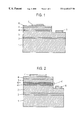
- FIG. 1 is a cross sectional view showing the structure of a GaN group compound-semiconductor, light-emitting device in accordance with a first embodiment of the present invention.
- a buffer layer 2 is formed on a sapphire substrate 1 .
- an n-type layer 3 On the buffer layer 2 , an n-type layer 3 , a light-emitting layer 4 , a p-type clad layer 5 and a p-type contact layer 6 are formed, in order from the bottom, by a metal organic CVD method.
- a p-side electrode 7 is formed on the p-type contact layer 6
- an n-side electrode 8 is formed on the surface of the n-type layer 3 , which is exposed as a result of etching-off part of the p-type clad layer 5 and the light-emitting layer 4 .
- the n-side electrode 7 may be formed of aluminum(Al), titanium(Ti) and other metals.
- Each of the p-side and n-side electrodes may be formed by means of metal deposition.
- the buffer layer 2 GaN, GaAlN, AlN, AlInN and the like may be used.
- the light-emitting layer 4 is formed of InGaN, and is doped with Mg, as the p-type impurity, to a certain predetermined concentration range.
- the p-type clad layer 5 AlGaN, GaN, AlGaInN and the like may be used.
- the p-type contact layer 6 GaN, InGaN and the like may be used. Mg is used as the p-type impurity for doping the p-type clad layer 5 and the p-type contact layer 6 .
- the light-emitting layer 4 is doped with the impurity Mg.
- the Mg doping is performed through diffusion from the p-type layer.
- a deep p-type impurity level may not be formed in a light-emitting device. Therefore, a light-emitting layer 4 is obtained in which a light emission that is related to the acceptor level is difficult to occur.
- the Mg doping is conducted by means of diffusion from the p-type layer, it is easier to prevent the light-emitting layer 4 from being doped for the entire part at a high concentration level, as compared with a case where the light-emitting layer 4 is doped direct with Mg. As such, a state of graded concentration, where the Mg concentration is gradually decreasing from a side having contact with p-type layer towards the side having contact with n-type layer 3 , is easily provided.
- the light-emitting layer 4 of GaN group compound-semiconductor tends to exhibit the n-type conduction while it is un-doped.
- a p-type conduction is provided at the p-type layer side, where the concentration is high, while an n-type conduction is provided at the n-type layer side, where the concentration is low.
- a pn junction is formed within the light-emitting layer 4 .
- the light-emitting layer 4 is made of InGaN, which does not contain Al. If Al is included, the crystalline property tends to degrade, which leads to a degradation of light-emitting layer 4 .
- a light emission caused by the electron transition between conduction band and valence band is obtained, without using the light emission related to the acceptor level formed by a p-type impurity, if the light-emitting layer 4 is doped with a p-type impurity in a concentration level at which the acceptor level is not formed.
- the research also revealed that the improvements are made in both the luminous efficiency and the color purity when the concentration of Mg, or a p-type impurity, is controlled to be within a range, not lower than 1 ⁇ 10 16 cm ⁇ 3 and not higher than 5 ⁇ 10 20 cm ⁇ 3 .
- the light emission related to the impurity level such as the D-A pair light emission
- the Mg concentration of the impurity level is not used in the area where the Mg concentration is not higher than 1 ⁇ 10 16 cm ⁇ 3
- the wavelength of the light emitted at the above Mg concentration area is identical to that of un-doped state, where a light due to the electron transition between conduction band and valence band is exhibited. If the Mg concentration of a light-emitting layer is not lower than 5 ⁇ 10 20 cm ⁇ 3 , a light emission related to the acceptor level is dominant.
- a light emission caused by the electron transition between conduction band and valence band is obtained by doping the Mg so that the concentration falls within a certain specified range.
- the light thus emitted has a spectrum that is sharper as compared with that of a light emitted in relation to the impurity level.
- the peak wavelength of the former light hardly shifts to the short wavelength side even when the operating current is increased. The color purity is improved.
- a pn junction is formed within the light-emitting layer 4 .
- a light-emitting device of high luminous efficiency is presented.
- the formation of the pn junction in the n-type layer 3 is prevented, by lowering the concentration of Mg, or p-type impurity, at the side having contact with the n-type layer 3 . If the Mg concentration at the side having contact with p-type layer is high, the efficiency of current injection into light-emitting layer 4 may be made high, which leads to a still higher luminous efficiency.
- a p-type impurity, to be doped into a light-emitting layer 4 By controlling the concentration of Mg, a p-type impurity, to be doped into a light-emitting layer 4 to be within the above described range, (i.e., not lower than 1 ⁇ 10 16 cm ⁇ 3 and not higher than 5 ⁇ 10 20 cm ⁇ 3 ), both of the luminous efficiency and the color purity are improved.
- the Mg concentration at the side having contact with the n-type layer 3 is above 1 ⁇ 10 18 cm ⁇ 3 the light-emitting layer 4 tends to exhibit the p-type in its whole structure, and the luminous intensity goes down. If the Mg concentration is lower than 1 ⁇ 10 16 cm ⁇ 3 , the pn junction could be formed inclined towards the p-type layer, or the light-emitting layer 4 as a whole could exhibit the n-type, rendering it to have a high resistance. This also degrades the luminous intensity.
- the Mg concentration at the side having contact with the p-type layer is above 5 ⁇ 10 20 cm ⁇ 3 , a light emission related to the acceptor level is observed and the color purity tends to be degraded. If the Mg concentration at the side having contact with the p-type layer is lower than 1 ⁇ 10 18 cm ⁇ 3 , it turns out to be difficult to make the region into the p-type, and therefor a pn junction cannot be formed within the light-emitting layer 4 . The luminous intensity tends to degrade.
- the light-emitting layer of the present invention should preferably be doped with no n-type impurity.
- concentration of a p-type impurity, Mg, to be doped into the p-type layer is controlled to meet the above described conditions, the influence of an n-type impurity, if doped for a small quantity, remains to be negligibly small. So, the formation of pn junction within the light-emitting layer is possible.
- the improvements in both aspects, the luminous intensity and the color purity, may be expected so long as the doping stays at a level where the p-type conduction is preserved at the side of light-emitting layer having contact with p-type layer.
- the present embodiment refers to a method of growing a GaN group compound-semiconductor by a metal organic CVD method. Reference is made to FIG. 1 .
- a sapphire substrate 1 having a mirror-polished surface is set on a substrate holder within a reaction tube.
- the substrate 1 is maintained at 1100° C. on the surface for 10 minutes, and is cleaned to remove any organic substance and other stains sticking on the surface by heating the substrate in hydrogen gas flow.
- the surface temperature of the substrate 1 is lowered down to 600° C., and a buffer layer 2 of AlN is grown to a thickness of 25 nm by providing nitrogen gas, as the main carrier gas, at 10 liter/min., ammonia at 5 liter/min. and a TMA carrier gas containing tri-methyl-aluminum(TMA) at 20 cc/min.
- TMA carrier gas The supply of the TMA carrier gas is discontinued and the temperature is raised up-to 1050° C. Then, while continuing the flow of nitrogen gas at 9 liter/min., and hydrogen gas at 0.95 liter/min., new gases are provided, namely, a carrier gas of tri-methyl-gallium(TMG) at 4 cc/min., a 10 ppm SiH 4 (mono-silane) gas, as the source of Si, at 10 cc/min. for a duration of 60 min. in order to grow an n-type layer 3 of Si doped GaN to a thickness of approximately 2 ⁇ m.
- TMG tri-methyl-gallium
- SiH 4 mono-silane
- the supply of TMG carrier gas and the SiH 4 gas is discontinued, the surface temperature of the substrate is lowered down to 750° C., and then, nitrogen gas, as the main carrier gas, is newly provided at 10 liter/min., a carrier gas of TMG at 2 cc/min., and a carrier gas of tri-methyl-indium(TMI) at 200 cc/min. for a duration of 100 sec. in order to grow a light-emitting layer 4 of InGaN to a thickness of 10 nm.
- the TMI carrier gas and the TMG carrier gas are discontinued, the surface temperature of the substrate 1 is raised up-to 1050° C., and nitrogen gas, as the main carrier gas, is newly provided at 9 liter/min., hydrogen gas at 0.90 liter/min., a TMG carrier gas at 4 cc/min., a TMA carrier gas at 6 cc/min., a carrier gas of bis-cyclo-pentadienyel-magnesium(Cp 2 Mg), or the Mg source, at 60 cc/min. for a duration of 4 min. in order to grow a p-type clad layer 5 of Mg doped AlGaN to a thickness of 0.1 ⁇ m.
- the TMA carrier gas, the TMG carrier gas and the Cp 2 Mg carrier gas are discontinued.
- the substrate temperature is maintained at 1050° C. for a duration of 10 min. to diffuse the Mg doped in the p-type clad layer 5 into the light-emitting layer 4 .
- Maintaining the temperature 1050° C., nitrogen gas, as the main carrier gas, is newly provided at 9 liter/min., hydrogen gas at 0.90 liter/min., a TMG carrier gas at 4 cc/min. and a Cp 2 Mg carrier gas at 100 cc/min. for a duration of 3 min. in order to grow a p-type contact layer of Mg doped GaN in the thickness of 0.1 ⁇ m.
- the supply of material gases, a TMG carrier gas, a Cp 2 Mg carrier gas, and ammonia is discontinued.
- the flow of nitrogen gas and hydrogen gas is maintained at the same flow rate until the wafer is cooled down to the room temperature. The wafer is then taken out of the reaction tube.
- a SiO 2 film is deposited by a CVD method.
- An etching mask is provided by patterning the film through a photo lithographic process.
- the p-type contact layer 6 , the p-type clad layer 5 and the light-emitting layer 4 are partially etched-off by a reactive ion etching method in the depth of approximately 0.25 ⁇ m to expose the surface of n-type layer 3 .
- an n-side electrode 8 of Al is formed using photo-lithography and deposition.
- a p-side electrode 7 of Ni and Au is formed on the surface of p-type contact layer 6 .
- the sapphire substrate 1 is polished in the reverse surface down to approximately 100 ⁇ m thick, and separated into chips by scribing.
- a light-emitting device thus manufactured comprises a pn junction formed within the light-emitting layer 4 .
- the Mg concentration has a graded distribution; which equals 1 ⁇ 10 19 cm ⁇ 3 , at a side having contact with p-type clad layer 5 and which gradually decreases down to 2 ⁇ 10 17 cm ⁇ 3 at the side having contact with n-type layer 3 .
- a separated chip is attached on a stem with the surface having the electrode up.
- the respective n-side electrode 8 and p-side electrode 7 on the chip are connected with wire to electrodes of the stem, and the whole structure is resin-molded to complete a light-emitting diode.
- the light-emitting diode When the light-emitting diode is driven with 20 mA forward current, it emits a blue light of 450 nm wavelength; has a spectral half band width of 18 nm, and a luminous output 1100 ⁇ W.
- a light-emitting device has been manufactured in the same procedure as in the above embodiment, except that; in the process for growing light-emitting layer 4 and p-type clad layer 5 , a light-emitting layer 4 of n-type InGaN doped with Si and Zn has been grown to a thickness of 10 nm by newly providing, at 750° C., nitrogen gas, or the main carrier gas, at 10 liter/min., a TMG carrier gas at 2 cc/min., a carrier gas of tri-methyl-indium at 100 cc/min., SiH 4 gas at 10 cc/min., diethyl-zinc gas as the Zn source at 10 cc/min.
- the light-emitting diode is driven with 20 mA forward current, it emitted blue light of 450 nm wavelength.
- the spectral half band width of the diode is 50 nm, which is greater than that of the earlier embodiment.
- the color purity is also degraded, and the output of light emission is 710 ⁇ W.
- the diffusing operation of a p-type impurity contained in the p-type layer into a light-emitting layer 4 from the p-type layer containing the p-type impurity has been conducted by; first growing a p-type clad layer 5 , and then the substrate is kept at a certain temperature to diffuse Mg contained in the p-type clad layer 5 into the light-emitting layer 4 .
- FIG. 2 is a vertical sectional view showing the structure of a GaN group compound-semiconductor light-emitting device in accordance with another embodiment of the present invention.
- the layers of GaN compound-semiconductor film formed on the sapphire substrate remain the same as those of the prior art technology shown in FIG. 4, with the exception of a light-emitting layer.
- Those parts identical to those of the prior art are represented by providing the same marks, and detailed explanation of which is omitted here.
- a buffer layer 2 , an n-type clad layer 3 , a light-emitting layer 4 , a p-type clad layer 5 and a p-type contact layer 6 are stacked in layers on a sapphire substrate 1 .
- a p-side electrode 7 is formed on the p-type contact layer 6
- an n-side electrode 8 is formed on the surface of the n-type layer 3 exposed by partially etching-off the p-type clad layer 5 and the light-emitting layer 4 .
- the n-side electrode 8 can be formed of aluminum(Al), titanium(Ti) or such other metals.
- Each of the p-side and n-side electrodes 7 , 8 is formed by metal deposition.
- the light-emitting layer 4 is preferably formed with a GaN group compound-semiconductor such as InGaN, InGaAlN, whose band-gap energy is smaller than that of the n-type clad layer 3 and the p-type clad layer 5 . More specifically, an InGaN whose indium composition is optimized for providing a band-gap energy suitable to generate a light of desired wavelength is preferred.
- the light-emitting layer 4 has been formed as a double-layered structure consisting of an n-type layer 41 having contact with the n-type clad layer 3 and a p-type layer 42 stacked on the n-type layer 41 and having contact at the upper surface with the p-type clad layer 5 .
- the n-type layer 41 has been formed to exhibit an n-type conduction, by either doping an n-type impurity such as Si, Ge during the earlier described CVD process of InGaN, InGaAlN and other GaN group compound-semiconductors, or not doping any n-type impurity, leaving it as an “undoped”.
- the GaN group compound-semiconductor can be made to exhibit an n-type conduction without doping Si, Ge or any other n-type impurity. Doping of an n-type impurity may enhance the efficiency of electron injection into a light-emitting layer 4 .
- the p-type layer 42 has been formed to exhibit a p-type conduction by doping Mg during the CVD process of InGaN, InGaAlN and other GaN group compound-semiconductors.
- Mg the impurities of Zn, Cd, Be, Ca, C, etc. may also be used as the p-type dcopant.
- Mg is used as the dopant, for which material the deep level formation within the light-emitting layer 4 is difficult, a light emission using the band-to-band transition in the light-emitting layer 4 is readily available, and the efficiency of light emission goes higher. Therefore, it is preferred to use Mg as the dopant in view of improving the luminance.
- the n-type clad layer 3 which is locating under the light-emitting layer 4 and having the n-type layer 41 stacked thereon, is that it is a GaN group compound-semiconductor whose band gap energy is greater than that of light-emitting layer 4 .
- GaN, InGaN, InGaAlN etc., for example, can be utilized.
- the p-type clad layer 5 which is locating on the light-emitting layer 4 and stacked on the surface of the p-type layer 42 , is that it is a GaN group compound-semiconductor whose band gap energy is greater than that of light-emitting layer.
- GaN, InGaN, AlGaN, InGaAlN, etc., for example, can be utilized.
- a pn junction is formed within the light-emitting layer 4 by the n-type layer 41 and the p-type layer 42 . Therefore, the injection of electrons and holes into a light-emitting layer 4 is expedited, and the re-combination of electrons and holes is readily performed within the light-emitting layer 4 . Thus the luminous efficiency is improved and the luminous intensity is raised.
- the double layered light-emitting layer 4 comprising the p-type layer 42 and the n-type layer 41 has contact at the n-type layer 41 with n-type clad layer 3 , while at the p-typo layer 42 with p-type clad layer 5 .
- a pn junction is formed without fail inside of the light-emitting layer 4 , electrons are injected efficiently into the light-emitting layer from the n-type clad layer 3 , and holes are injected efficiently into the light-emitting layer 4 from the p-type clad layer 5 .
- the re-combination of electrons and holes within the light-emitting layer 4 readily occurs, and the luminous efficiency is improved a step higher.
- FIG. 3 is a vertical sectional view of a GaN group compound-semiconductor light-emitting device in accordance with a third exemplary embodiment of the present invention. Those parts identical to those of FIG. 2 are represented by providing the same reference numerals, and detailed explanation of which is omitted here.
- the light-emitting layer 4 of the present embodiment further comprises an i-type layer 43 in between the layers 41 and 42 , forming a three-layered structure. This is the only difference from the structure shown In FIG. 2 .
- the i-type layer 43 refers to either a p-type layer having a high resistivity and a very low carrier concentration, or an n-type layer.
- the i-type layer 43 can be provided as a layer of very low carrier concentration by doping an n-type impurity such as Si, Ge, and a p-type impurity such as Mg at a same time, or causing a carrier compensation through the doping of a small quantity of p-type impurity, such as Mg, without doping any n-type impurity.
- the simultaneous doping of n-type impurity and p-type impurity can be accomplished by supplying the material gases of n-type impurity and p-type impurity together during the crystalline growth of light-emitting layer 4 .
- a region which is doped with n-type and p-type impurities or with p-type impurity alone at a low concentration is formed, during formation of the p-type layer 42 doped with p-type impurity and the p-type clad layer 5 , by diffusing the p-type impurities contained in these p-type layers into part of the n-type layer.
- the region is provided in a layered form, making it as the i-type layer.
- the light-emitting layer 4 of a three-layered structure comprising the n-type layer 41 , the i-type layer 43 and the p-type layer 42 , a pn junction is formed within of the light-emitting layer 4 , because the n-type layer 41 and the p-type layer 42 are disposed with the i-type layer 43 of very low carrier concentration in between them.
- the re-combination of electrons and holes is therefore expedited within the light-emitting layer 4 , and the luminous intensity is increased.
- the n-type clad layer 3 , the light-emitting layer 4 and the p-type clad layer 5 are stacked, in order from the bottom, on the substrate 1 via the buffer layer 2 , it can also be structured such that the n-type clad layer 3 and the p-type clad layer 5 are exchanged with each other.
- the p-type clad layer 5 , the light-emitting layer 4 and the n-type clad layer 3 may be stacked in order from the substrate 1 , the light-emitting layer 4 being provided with a p-type layer 42 at the side of p-type clad layer 5 and an n-type layer 41 at the side of n-type layer 3 , respectively.
- the specimen device containing the i-type layer 43 as shown in FIG. 3 can be structured in a similar manner.
- a sapphire substrate 1 having a mirror-polished surface is set on a substrate holder within a reaction tube.
- the substrate 1 is maintained at 1100° C. on the surface for 10 minutes, and cleaned to remove organic substance and other stains sticking on the surface by heating the substrate in a hydrogen gas flow.
- a buffer layer 2 of AlN is grown to a thickness of 25 nm by providing nitrogen gas, as the main carrier gas, at 10 liter/min., ammonia at 5 liter/min. and a TMA carrier gas containing tri-methyl-aluminum(TMA) at 20 cc/min.
- TMA carrier gas The supply of the TMA carrier gas is discontinued and the temperature is raised up-to 1050° C. Then, while continuing the flow of nitrogen gas at 9 liter/min., and hydrogen gas at 0.95 liter/min., new gases are added, namely, a carrier gas of tri-methyl-gallium(TMG) at 4 cc/min., a 10 ppm SiH 4 (mono-silane) gas, as the source of Si, at 10 cc/min. for a duration of 60 min. in order to grow an n-type layer 3 of Si doped GaN to a thickness of 2 ⁇ m.
- TMG tri-methyl-gallium
- SiH 4 mono-silane
- the supply of TMG carrier gas and the SiH 4 gas is discontinued, the surface temperature of substrate 1 is lowered down to 750° C., and new gases are provided; nitrogen gas, as the main carrier gas, at 10 liter/min., a TMG carrier gas at 2 cc/min., and a TMI(tri-methyl-indium) carrier gas at 200 cc/min. for a duration of 60 sec. in order to grow an “undoped” and n-type light-emitting layer 4 of InGaN to a thickness of 6 nm.
- the TMI carrier gas and the TMG carrier gas are discontinued, the surface temperature of substrate 1 is raised up-to 1050° C., and new gases are provided; nitrogen gas, as the main carrier gas, at 9 liter/min., hydrogen gas at 0.90 liter/min., a TMG carrier gas at 4 cc/min., a TMA carrier gas at 6 cc/min., a carrier gas of bis-cyclo-pentadienyel-magnesium(Cp 2 Mg), as Mg source, at 60 cc/min. for a duration of 4 min. in order to grow a p-type clad layer 5 of Mg doped AlGaN to a thickness of 0.1 ⁇ m.
- the TMA carrier gas, the TMG carrier gas and the Cp 2 Mg carrier gas are discontinued.
- the substrate temperature is maintained at 1050° C. for a duration of 8 min. to diffuse the Mg doped in the p-type clad layer 5 into the light-emitting layer 4 , in order to form a p-type layer 42 at the side of light-emitting layer 4 having contact with p-type clad layer 5 in the thickness of approximately 3 nm, and an n-type layer 41 at the side of light-emitting layer 4 having contact with n-type clad layer 3 in the thickness of approximately 3 nm.
- the light-emitting layer 4 thus formed comprises stacked layers, namely, the n-type layer 41 and the p-type layer 42 .
- Maintaining the temperature at 1050° C., nitrogen gas, as the main carrier gas, is newly provided at 9 liter/min., hydrogen gas at 0.90 liter/min., a TMG carrier gas at 4 cc/min. and a Cp 2 Mg carrier gas at 100 cc/min. for a duration of 3 min. in order to grow a p-type contact layer 6 of Mg doped GaN to a thickness of 0.1 ⁇ m.
- the supply of material gases, TMG carrier gas, Cp 2 Mg carrier gas, and ammonia is discontinued, while the flow of nitrogen gas and hydrogen gas is maintained at the same flow rate until the wafer is cooled down to the room temperature. The wafer is then taken out of the reaction tube.
- a SiO 2 film is deposited by a CVD method.
- the film is patterned in a certain predetermined shape by a photo lithographic process to provide an etching mask.
- the p-type contact layer 6 , the p-type clad layer 5 and the light-emitting layer 4 are partially etched-off by a reactive ion etching method in the depth of approximately 0.25 ⁇ m to expose the surface of the n-type layer 3 .
- an n-side electrode 8 of Al is formed by deposition.
- a p-side electrode 7 of Ni and Au is formed on the surface of p-type contact layer 6 .
- the sapphire substrate 1 is polished in the reverse surface down to approximately 100 ⁇ m thick, and separated into chips by scribing.
- a light-emitting device as shown in FIG. 2 is provided through the above described procedure.
- a GaN group compound-semiconductor light-emitting device thus manufactured is attached on a stem with the surface having the electrode up.
- the respective n-side electrode 8 and p-side electrode 7 on the chip are connected with wire to electrodes of the stem, and the whole structure is resin-molded to complete a light-emitting diode.
- the light-emitting diode When the light-emitting diode is driven with 20 mA forward current, it emits a blue light of 455 nm wavelength; has a spectral half band width of 18 nm, and a luminous output of 1050 ⁇ W.
- nitrogen gas as the main carrier gas, is newly provided at 10 liter/min., a TMG carrier gas at 2 cc/min. and a TMI carrier gas at 200 cc/min. at a temperature 750° C.
- SiH 4 gas is provided in a linear declining mode starting from at 10 cc/min. down to 0.1 cc/min. for a duration of 70 sec. to grow part of light-emitting layer 4 of InGaN to a thickness of 70 nm.
- the SiH 4 gas is discontinued, while the TMG carrier gas and the TMI carrier gas are kept flowing at the same flow rate for a duration of 130 sec. to grow the remaining part of the light-emitting layer 4 to a thickness of 130 nm.
- the TMI carrier gas and the TMG carrier gas are discontinued, the surface temperature of substrate 1 is raised up-to 1050° C., nitrogen gas, as the main carrier gas, is newly provided at 9 liter/min., hydrogen gas at 0.90 liter/min., a TMG carrier gas at 4 cc/min., a TMA carrier gas at 6 cc/min., a Cp 2 Mg carrier gas at 60 cc/min., for a duration of 4 min. in order to grow a p-type clad layer 5 of Mg doped AlGaN to a thickness of 0.1 ⁇ m.
- the light-emitting layer 4 is formed so as to comprise stacked layers, namely, the n-type layer 41 , the i-type layer 43 and the p
- a light-emitting device of FIG. 3 is completed after an electrode is formed thereon, and separated into chips, in the same way as in embodiment 2.
- a light-emitting diode is fabricated in the same as in embodiment 1, and driven with a 20 mA forward current, it emits a blue light of 445 nm wavelength; has a spectral half band width of 17 nm, and a luminous output 1150 ⁇ W.
Abstract
Description
Claims (10)
Applications Claiming Priority (4)
| Application Number | Priority Date | Filing Date | Title |
|---|---|---|---|
| JP10-034474 | 1998-02-17 | ||
| JP3447498A JP2950316B2 (en) | 1998-02-17 | 1998-02-17 | Gallium nitride based compound semiconductor light emitting device and method of manufacturing the same |
| JP12570898A JP3684841B2 (en) | 1998-05-08 | 1998-05-08 | Gallium nitride compound semiconductor light emitting device |
| JP10-125708 | 1998-05-08 |
Publications (1)
| Publication Number | Publication Date |
|---|---|
| US6445127B1 true US6445127B1 (en) | 2002-09-03 |
Family
ID=26373290
Family Applications (1)
| Application Number | Title | Priority Date | Filing Date |
|---|---|---|---|
| US09/250,732 Expired - Lifetime US6445127B1 (en) | 1998-02-17 | 1999-02-16 | Light-emitting device comprising gallium-nitride-group compound-semiconductor and method of manufacturing the same |
Country Status (1)
| Country | Link |
|---|---|
| US (1) | US6445127B1 (en) |
Cited By (12)
| Publication number | Priority date | Publication date | Assignee | Title |
|---|---|---|---|---|
| US20030160246A1 (en) * | 2002-02-25 | 2003-08-28 | Jagdish Narayan | Efficient light emitting diodes and lasers |
| US20030222263A1 (en) * | 2002-06-04 | 2003-12-04 | Kopin Corporation | High-efficiency light-emitting diodes |
| US20040072381A1 (en) * | 2002-06-28 | 2004-04-15 | Kopin Corporation | Domain epitaxy for thin film growth |
| US20040075097A1 (en) * | 1998-06-05 | 2004-04-22 | Goetz Werner K. | Formation of Ohmic contacts in III-nitride light emitting devices |
| US20050052878A1 (en) * | 2003-09-05 | 2005-03-10 | Motokazu Yamada | Lighting device and lighting fixture for a vehicle |
| US20050179046A1 (en) * | 2004-02-13 | 2005-08-18 | Kopin Corporation | P-type electrodes in gallium nitride-based light-emitting devices |
| US20050179042A1 (en) * | 2004-02-13 | 2005-08-18 | Kopin Corporation | Monolithic integration and enhanced light extraction in gallium nitride-based light-emitting devices |
| US20060097283A1 (en) * | 2003-09-16 | 2006-05-11 | Tetsuya Taki | Group III-nitride-based compound semiconductor device |
| US7122841B2 (en) | 2003-06-04 | 2006-10-17 | Kopin Corporation | Bonding pad for gallium nitride-based light-emitting devices |
| US20070045654A1 (en) * | 2005-08-30 | 2007-03-01 | Samsung Electro-Mechanics Co., Ltd. | Group III-nitride semiconductor thin film, method for fabricating the same, and group III-nitride semiconductor light emitting device |
| US20120228581A1 (en) * | 2011-03-08 | 2012-09-13 | Kabushiki Kaisha Toshiba | Semiconductor light emitting device and manufacturing method of the same |
| US10283346B2 (en) * | 2016-03-08 | 2019-05-07 | Enraytek Optoelectronics Co., Ltd. | Sapphire substrate recycling method |
Citations (6)
| Publication number | Priority date | Publication date | Assignee | Title |
|---|---|---|---|---|
| JPH06260680A (en) | 1993-03-05 | 1994-09-16 | Nichia Chem Ind Ltd | Gallium nitride compound semiconductor light emitting element |
| JPH0846240A (en) | 1994-07-28 | 1996-02-16 | Toyoda Gosei Co Ltd | Group iii nitride semiconductor light emitting element |
| JPH09186362A (en) | 1995-12-28 | 1997-07-15 | Toyoda Gosei Co Ltd | Iii nitride semiconductor light emitting element |
| JPH1032347A (en) | 1997-03-31 | 1998-02-03 | Toyoda Gosei Co Ltd | Semiconductor light emitting element of compound of nitrogen and group iii element |
| US5729029A (en) * | 1996-09-06 | 1998-03-17 | Hewlett-Packard Company | Maximizing electrical doping while reducing material cracking in III-V nitride semiconductor devices |
| JPH1117222A (en) | 1997-06-23 | 1999-01-22 | Showa Denko Kk | Compound semiconductor light-emitting device |
-
1999
- 1999-02-16 US US09/250,732 patent/US6445127B1/en not_active Expired - Lifetime
Patent Citations (6)
| Publication number | Priority date | Publication date | Assignee | Title |
|---|---|---|---|---|
| JPH06260680A (en) | 1993-03-05 | 1994-09-16 | Nichia Chem Ind Ltd | Gallium nitride compound semiconductor light emitting element |
| JPH0846240A (en) | 1994-07-28 | 1996-02-16 | Toyoda Gosei Co Ltd | Group iii nitride semiconductor light emitting element |
| JPH09186362A (en) | 1995-12-28 | 1997-07-15 | Toyoda Gosei Co Ltd | Iii nitride semiconductor light emitting element |
| US5729029A (en) * | 1996-09-06 | 1998-03-17 | Hewlett-Packard Company | Maximizing electrical doping while reducing material cracking in III-V nitride semiconductor devices |
| JPH1032347A (en) | 1997-03-31 | 1998-02-03 | Toyoda Gosei Co Ltd | Semiconductor light emitting element of compound of nitrogen and group iii element |
| JPH1117222A (en) | 1997-06-23 | 1999-01-22 | Showa Denko Kk | Compound semiconductor light-emitting device |
Cited By (21)
| Publication number | Priority date | Publication date | Assignee | Title |
|---|---|---|---|---|
| US20040075097A1 (en) * | 1998-06-05 | 2004-04-22 | Goetz Werner K. | Formation of Ohmic contacts in III-nitride light emitting devices |
| US6914272B2 (en) * | 1998-06-05 | 2005-07-05 | Lumileds Lighting U.S., Llc | Formation of Ohmic contacts in III-nitride light emitting devices |
| US20050167693A1 (en) * | 1998-06-05 | 2005-08-04 | Goetz Werner K. | Formation of Ohmic contacts in III-nitride light emitting devices |
| US7345323B2 (en) | 1998-06-05 | 2008-03-18 | Philips Lumileds Lighting Company Llc | Formation of Ohmic contacts in III-nitride light emitting devices |
| US20030160246A1 (en) * | 2002-02-25 | 2003-08-28 | Jagdish Narayan | Efficient light emitting diodes and lasers |
| US20030222263A1 (en) * | 2002-06-04 | 2003-12-04 | Kopin Corporation | High-efficiency light-emitting diodes |
| US20040072381A1 (en) * | 2002-06-28 | 2004-04-15 | Kopin Corporation | Domain epitaxy for thin film growth |
| US6955985B2 (en) | 2002-06-28 | 2005-10-18 | Kopin Corporation | Domain epitaxy for thin film growth |
| US7122841B2 (en) | 2003-06-04 | 2006-10-17 | Kopin Corporation | Bonding pad for gallium nitride-based light-emitting devices |
| US20050052878A1 (en) * | 2003-09-05 | 2005-03-10 | Motokazu Yamada | Lighting device and lighting fixture for a vehicle |
| US7193358B2 (en) * | 2003-09-05 | 2007-03-20 | Nichia Corporation | Light-emitting device arranged in the light distribution pattern for a vehicle |
| US20060097283A1 (en) * | 2003-09-16 | 2006-05-11 | Tetsuya Taki | Group III-nitride-based compound semiconductor device |
| US20050179042A1 (en) * | 2004-02-13 | 2005-08-18 | Kopin Corporation | Monolithic integration and enhanced light extraction in gallium nitride-based light-emitting devices |
| US20050179046A1 (en) * | 2004-02-13 | 2005-08-18 | Kopin Corporation | P-type electrodes in gallium nitride-based light-emitting devices |
| US20070045654A1 (en) * | 2005-08-30 | 2007-03-01 | Samsung Electro-Mechanics Co., Ltd. | Group III-nitride semiconductor thin film, method for fabricating the same, and group III-nitride semiconductor light emitting device |
| US20100055883A1 (en) * | 2005-08-30 | 2010-03-04 | Samsung Electro-Mechanics Co., Ltd. | Group iii-nitride semiconductor thin film, method for fabricating the same, and group iii-nitride semiconductor light emitting device |
| US7687814B2 (en) | 2005-08-30 | 2010-03-30 | Samsung Electro-Mechanics Co., Ltd. | Group III-nitride semiconductor thin film, method for fabricating the same, and group III-nitride semiconductor light emitting device |
| US7955957B2 (en) | 2005-08-30 | 2011-06-07 | Samsung Led Co., Ltd. | Group III-nitride semiconductor thin film, method for fabricating the same, and group III-nitride semiconductor light emitting device |
| US20120228581A1 (en) * | 2011-03-08 | 2012-09-13 | Kabushiki Kaisha Toshiba | Semiconductor light emitting device and manufacturing method of the same |
| US8729575B2 (en) * | 2011-03-08 | 2014-05-20 | Kabushiki Kaisha Toshiba | Semiconductor light emitting device and manufacturing method of the same |
| US10283346B2 (en) * | 2016-03-08 | 2019-05-07 | Enraytek Optoelectronics Co., Ltd. | Sapphire substrate recycling method |
Similar Documents
| Publication | Publication Date | Title |
|---|---|---|
| KR100458145B1 (en) | Semiconductor light emitting device and method for manufacturing same | |
| JP4341702B2 (en) | Group III nitride semiconductor light emitting device | |
| JP3780887B2 (en) | Semiconductor light emitting device and manufacturing method thereof | |
| JPH0715041A (en) | Light emitting element of gallium nitride based compound semiconductor | |
| JPH0823124A (en) | Light-emitting element of gallium nitride compound semiconductor | |
| US6307219B1 (en) | Light-emitting device comprising gallium-nitride-group compound semiconductor | |
| US6445127B1 (en) | Light-emitting device comprising gallium-nitride-group compound-semiconductor and method of manufacturing the same | |
| US7002184B2 (en) | Light-emitting device comprising a gallum-nitride-group compound-semiconductor | |
| JP2713095B2 (en) | Semiconductor light emitting device and method of manufacturing the same | |
| JP2007281057A (en) | Laminate structure of group iii nitride semiconductor and its manufacturing method, and semiconductor light-emitting element and its manufacturing method | |
| US6429032B1 (en) | Nitride semiconductor and a method thereof, a nitride semiconductor device and a method thereof | |
| JP3504976B2 (en) | Semiconductor light emitting device | |
| JP3763701B2 (en) | Gallium nitride semiconductor light emitting device | |
| JP3216596B2 (en) | Gallium nitride based compound semiconductor light emitting device | |
| JP2000174341A (en) | Gallium nitride based compound semiconductor light- emitting element | |
| JPH05343737A (en) | Manufacture of semiconductor light emitting element | |
| JP2950316B2 (en) | Gallium nitride based compound semiconductor light emitting device and method of manufacturing the same | |
| JP2003008059A (en) | Nitride-family semiconductor light-emitting element | |
| KR20010008570A (en) | GaN Semiconductor Device of Quantum Well structure | |
| JP3025760B2 (en) | Gallium nitride based semiconductor laser device and method of manufacturing the same | |
| JP3684841B2 (en) | Gallium nitride compound semiconductor light emitting device | |
| JP4055794B2 (en) | Gallium nitride compound semiconductor light emitting device | |
| KR100337197B1 (en) | III-Nitride Semiconductor White Light Emitting Device | |
| JPH11330633A (en) | Semiconductor light emitting device | |
| JP2005252309A (en) | Manufacturing method of gallium nitride based semiconductor light emitting element |
Legal Events
| Date | Code | Title | Description |
|---|---|---|---|
| AS | Assignment |
Owner name: MATSUSHITA ELECTRIC INDUSTRIAL CO. LTD., JAPAN Free format text: ASSIGNMENT OF ASSIGNORS INTEREST;ASSIGNORS:OKU, YASUNARI;KAMEI, HIDENORI;REEL/FRAME:010304/0949 Effective date: 19990405 |
|
| STCF | Information on status: patent grant |
Free format text: PATENTED CASE |
|
| FEPP | Fee payment procedure |
Free format text: PAYOR NUMBER ASSIGNED (ORIGINAL EVENT CODE: ASPN); ENTITY STATUS OF PATENT OWNER: LARGE ENTITY |
|
| FPAY | Fee payment |
Year of fee payment: 4 |
|
| FPAY | Fee payment |
Year of fee payment: 8 |
|
| FEPP | Fee payment procedure |
Free format text: PAYOR NUMBER ASSIGNED (ORIGINAL EVENT CODE: ASPN); ENTITY STATUS OF PATENT OWNER: LARGE ENTITY Free format text: PAYER NUMBER DE-ASSIGNED (ORIGINAL EVENT CODE: RMPN); ENTITY STATUS OF PATENT OWNER: LARGE ENTITY |
|
| FPAY | Fee payment |
Year of fee payment: 12 |