US6451658B2 - Graded layer for use in semiconductor circuits and method for making same - Google Patents
Graded layer for use in semiconductor circuits and method for making same Download PDFInfo
- Publication number
- US6451658B2 US6451658B2 US09/887,612 US88761201A US6451658B2 US 6451658 B2 US6451658 B2 US 6451658B2 US 88761201 A US88761201 A US 88761201A US 6451658 B2 US6451658 B2 US 6451658B2
- Authority
- US
- United States
- Prior art keywords
- layer
- graded
- region
- sputtering
- graded layer
- Prior art date
- Legal status (The legal status is an assumption and is not a legal conclusion. Google has not performed a legal analysis and makes no representation as to the accuracy of the status listed.)
- Expired - Lifetime
Links
- 238000000034 method Methods 0.000 title claims abstract description 32
- 239000004065 semiconductor Substances 0.000 title description 15
- 239000000463 material Substances 0.000 claims abstract description 82
- 239000000203 mixture Substances 0.000 claims abstract description 14
- 239000000758 substrate Substances 0.000 claims description 21
- 238000004544 sputter deposition Methods 0.000 claims description 19
- 238000005477 sputtering target Methods 0.000 claims description 18
- 238000000151 deposition Methods 0.000 claims description 16
- 230000008021 deposition Effects 0.000 claims description 7
- 238000004377 microelectronic Methods 0.000 claims description 5
- 230000004888 barrier function Effects 0.000 abstract description 7
- 230000007704 transition Effects 0.000 abstract description 7
- 239000004020 conductor Substances 0.000 abstract description 6
- 229910052721 tungsten Inorganic materials 0.000 description 16
- WFKWXMTUELFFGS-UHFFFAOYSA-N tungsten Chemical compound [W] WFKWXMTUELFFGS-UHFFFAOYSA-N 0.000 description 12
- 239000010937 tungsten Substances 0.000 description 12
- 230000015654 memory Effects 0.000 description 9
- IJGRMHOSHXDMSA-UHFFFAOYSA-N Atomic nitrogen Chemical compound N#N IJGRMHOSHXDMSA-UHFFFAOYSA-N 0.000 description 6
- 239000010936 titanium Substances 0.000 description 6
- XUIMIQQOPSSXEZ-UHFFFAOYSA-N Silicon Chemical compound [Si] XUIMIQQOPSSXEZ-UHFFFAOYSA-N 0.000 description 5
- 229910052757 nitrogen Inorganic materials 0.000 description 5
- 229910052710 silicon Inorganic materials 0.000 description 5
- 239000010703 silicon Substances 0.000 description 5
- QGZKDVFQNNGYKY-UHFFFAOYSA-N Ammonia Chemical compound N QGZKDVFQNNGYKY-UHFFFAOYSA-N 0.000 description 4
- 230000015572 biosynthetic process Effects 0.000 description 4
- 238000005229 chemical vapour deposition Methods 0.000 description 4
- 238000010586 diagram Methods 0.000 description 4
- 150000001875 compounds Chemical class 0.000 description 3
- 230000005669 field effect Effects 0.000 description 3
- 230000008569 process Effects 0.000 description 3
- 229910052719 titanium Inorganic materials 0.000 description 3
- XKRFYHLGVUSROY-UHFFFAOYSA-N Argon Chemical compound [Ar] XKRFYHLGVUSROY-UHFFFAOYSA-N 0.000 description 2
- RTAQQCXQSZGOHL-UHFFFAOYSA-N Titanium Chemical compound [Ti] RTAQQCXQSZGOHL-UHFFFAOYSA-N 0.000 description 2
- NRTOMJZYCJJWKI-UHFFFAOYSA-N Titanium nitride Chemical compound [Ti]#N NRTOMJZYCJJWKI-UHFFFAOYSA-N 0.000 description 2
- UGACIEPFGXRWCH-UHFFFAOYSA-N [Si].[Ti] Chemical compound [Si].[Ti] UGACIEPFGXRWCH-UHFFFAOYSA-N 0.000 description 2
- 229910021529 ammonia Inorganic materials 0.000 description 2
- IVHJCRXBQPGLOV-UHFFFAOYSA-N azanylidynetungsten Chemical compound [W]#N IVHJCRXBQPGLOV-UHFFFAOYSA-N 0.000 description 2
- 230000008901 benefit Effects 0.000 description 2
- 239000000470 constituent Substances 0.000 description 2
- 230000000694 effects Effects 0.000 description 2
- -1 for example Substances 0.000 description 2
- 230000006870 function Effects 0.000 description 2
- 239000007789 gas Substances 0.000 description 2
- 239000011159 matrix material Substances 0.000 description 2
- 238000012986 modification Methods 0.000 description 2
- 230000004048 modification Effects 0.000 description 2
- 238000000926 separation method Methods 0.000 description 2
- 229910021332 silicide Inorganic materials 0.000 description 2
- FVBUAEGBCNSCDD-UHFFFAOYSA-N silicide(4-) Chemical compound [Si-4] FVBUAEGBCNSCDD-UHFFFAOYSA-N 0.000 description 2
- 229910021341 titanium silicide Inorganic materials 0.000 description 2
- MAKDTFFYCIMFQP-UHFFFAOYSA-N titanium tungsten Chemical compound [Ti].[W] MAKDTFFYCIMFQP-UHFFFAOYSA-N 0.000 description 2
- 229910052581 Si3N4 Inorganic materials 0.000 description 1
- UQZIWOQVLUASCR-UHFFFAOYSA-N alumane;titanium Chemical compound [AlH3].[Ti] UQZIWOQVLUASCR-UHFFFAOYSA-N 0.000 description 1
- 229910052786 argon Inorganic materials 0.000 description 1
- WYEMLYFITZORAB-UHFFFAOYSA-N boscalid Chemical compound C1=CC(Cl)=CC=C1C1=CC=CC=C1NC(=O)C1=CC=CN=C1Cl WYEMLYFITZORAB-UHFFFAOYSA-N 0.000 description 1
- 239000003990 capacitor Substances 0.000 description 1
- 230000008859 change Effects 0.000 description 1
- 238000007796 conventional method Methods 0.000 description 1
- 230000032798 delamination Effects 0.000 description 1
- 238000009792 diffusion process Methods 0.000 description 1
- 238000005530 etching Methods 0.000 description 1
- 238000005468 ion implantation Methods 0.000 description 1
- 238000001465 metallisation Methods 0.000 description 1
- 150000004767 nitrides Chemical class 0.000 description 1
- 125000002524 organometallic group Chemical group 0.000 description 1
- 238000004806 packaging method and process Methods 0.000 description 1
- 230000002093 peripheral effect Effects 0.000 description 1
- 229920002120 photoresistant polymer Polymers 0.000 description 1
- 238000000623 plasma-assisted chemical vapour deposition Methods 0.000 description 1
- 229910021420 polycrystalline silicon Inorganic materials 0.000 description 1
- 229920005591 polysilicon Polymers 0.000 description 1
- 238000012545 processing Methods 0.000 description 1
- 238000011160 research Methods 0.000 description 1
- WQJQOUPTWCFRMM-UHFFFAOYSA-N tungsten disilicide Chemical compound [Si]#[W]#[Si] WQJQOUPTWCFRMM-UHFFFAOYSA-N 0.000 description 1
- NXHILIPIEUBEPD-UHFFFAOYSA-H tungsten hexafluoride Chemical compound F[W](F)(F)(F)(F)F NXHILIPIEUBEPD-UHFFFAOYSA-H 0.000 description 1
- 229910021342 tungsten silicide Inorganic materials 0.000 description 1
Images


Classifications
-
- H—ELECTRICITY
- H01—ELECTRIC ELEMENTS
- H01L—SEMICONDUCTOR DEVICES NOT COVERED BY CLASS H10
- H01L21/00—Processes or apparatus adapted for the manufacture or treatment of semiconductor or solid state devices or of parts thereof
- H01L21/70—Manufacture or treatment of devices consisting of a plurality of solid state components formed in or on a common substrate or of parts thereof; Manufacture of integrated circuit devices or of parts thereof
- H01L21/71—Manufacture of specific parts of devices defined in group H01L21/70
- H01L21/768—Applying interconnections to be used for carrying current between separate components within a device comprising conductors and dielectrics
- H01L21/76838—Applying interconnections to be used for carrying current between separate components within a device comprising conductors and dielectrics characterised by the formation and the after-treatment of the conductors
- H01L21/76841—Barrier, adhesion or liner layers
-
- H—ELECTRICITY
- H01—ELECTRIC ELEMENTS
- H01L—SEMICONDUCTOR DEVICES NOT COVERED BY CLASS H10
- H01L21/00—Processes or apparatus adapted for the manufacture or treatment of semiconductor or solid state devices or of parts thereof
- H01L21/02—Manufacture or treatment of semiconductor devices or of parts thereof
- H01L21/04—Manufacture or treatment of semiconductor devices or of parts thereof the devices having at least one potential-jump barrier or surface barrier, e.g. PN junction, depletion layer or carrier concentration layer
- H01L21/18—Manufacture or treatment of semiconductor devices or of parts thereof the devices having at least one potential-jump barrier or surface barrier, e.g. PN junction, depletion layer or carrier concentration layer the devices having semiconductor bodies comprising elements of Group IV of the Periodic System or AIIIBV compounds with or without impurities, e.g. doping materials
- H01L21/28—Manufacture of electrodes on semiconductor bodies using processes or apparatus not provided for in groups H01L21/20 - H01L21/268
- H01L21/28008—Making conductor-insulator-semiconductor electrodes
- H01L21/28017—Making conductor-insulator-semiconductor electrodes the insulator being formed after the semiconductor body, the semiconductor being silicon
- H01L21/28026—Making conductor-insulator-semiconductor electrodes the insulator being formed after the semiconductor body, the semiconductor being silicon characterised by the conductor
- H01L21/28035—Making conductor-insulator-semiconductor electrodes the insulator being formed after the semiconductor body, the semiconductor being silicon characterised by the conductor the final conductor layer next to the insulator being silicon, e.g. polysilicon, with or without impurities
- H01L21/28044—Making conductor-insulator-semiconductor electrodes the insulator being formed after the semiconductor body, the semiconductor being silicon characterised by the conductor the final conductor layer next to the insulator being silicon, e.g. polysilicon, with or without impurities the conductor comprising at least another non-silicon conductive layer
-
- H—ELECTRICITY
- H01—ELECTRIC ELEMENTS
- H01L—SEMICONDUCTOR DEVICES NOT COVERED BY CLASS H10
- H01L21/00—Processes or apparatus adapted for the manufacture or treatment of semiconductor or solid state devices or of parts thereof
- H01L21/02—Manufacture or treatment of semiconductor devices or of parts thereof
- H01L21/04—Manufacture or treatment of semiconductor devices or of parts thereof the devices having at least one potential-jump barrier or surface barrier, e.g. PN junction, depletion layer or carrier concentration layer
- H01L21/18—Manufacture or treatment of semiconductor devices or of parts thereof the devices having at least one potential-jump barrier or surface barrier, e.g. PN junction, depletion layer or carrier concentration layer the devices having semiconductor bodies comprising elements of Group IV of the Periodic System or AIIIBV compounds with or without impurities, e.g. doping materials
- H01L21/28—Manufacture of electrodes on semiconductor bodies using processes or apparatus not provided for in groups H01L21/20 - H01L21/268
- H01L21/28008—Making conductor-insulator-semiconductor electrodes
- H01L21/28017—Making conductor-insulator-semiconductor electrodes the insulator being formed after the semiconductor body, the semiconductor being silicon
- H01L21/28026—Making conductor-insulator-semiconductor electrodes the insulator being formed after the semiconductor body, the semiconductor being silicon characterised by the conductor
- H01L21/28088—Making conductor-insulator-semiconductor electrodes the insulator being formed after the semiconductor body, the semiconductor being silicon characterised by the conductor the final conductor layer next to the insulator being a composite, e.g. TiN
-
- H—ELECTRICITY
- H01—ELECTRIC ELEMENTS
- H01L—SEMICONDUCTOR DEVICES NOT COVERED BY CLASS H10
- H01L29/00—Semiconductor devices adapted for rectifying, amplifying, oscillating or switching, or capacitors or resistors with at least one potential-jump barrier or surface barrier, e.g. PN junction depletion layer or carrier concentration layer; Details of semiconductor bodies or of electrodes thereof ; Multistep manufacturing processes therefor
- H01L29/40—Electrodes ; Multistep manufacturing processes therefor
- H01L29/43—Electrodes ; Multistep manufacturing processes therefor characterised by the materials of which they are formed
- H01L29/49—Metal-insulator-semiconductor electrodes, e.g. gates of MOSFET
- H01L29/4916—Metal-insulator-semiconductor electrodes, e.g. gates of MOSFET the conductor material next to the insulator being a silicon layer, e.g. polysilicon doped with boron, phosphorus or nitrogen
- H01L29/4925—Metal-insulator-semiconductor electrodes, e.g. gates of MOSFET the conductor material next to the insulator being a silicon layer, e.g. polysilicon doped with boron, phosphorus or nitrogen with a multiple layer structure, e.g. several silicon layers with different crystal structure or grain arrangement
- H01L29/4941—Metal-insulator-semiconductor electrodes, e.g. gates of MOSFET the conductor material next to the insulator being a silicon layer, e.g. polysilicon doped with boron, phosphorus or nitrogen with a multiple layer structure, e.g. several silicon layers with different crystal structure or grain arrangement with a barrier layer between the silicon and the metal or metal silicide upper layer, e.g. Silicide/TiN/Polysilicon
-
- H—ELECTRICITY
- H01—ELECTRIC ELEMENTS
- H01L—SEMICONDUCTOR DEVICES NOT COVERED BY CLASS H10
- H01L29/00—Semiconductor devices adapted for rectifying, amplifying, oscillating or switching, or capacitors or resistors with at least one potential-jump barrier or surface barrier, e.g. PN junction depletion layer or carrier concentration layer; Details of semiconductor bodies or of electrodes thereof ; Multistep manufacturing processes therefor
- H01L29/40—Electrodes ; Multistep manufacturing processes therefor
- H01L29/43—Electrodes ; Multistep manufacturing processes therefor characterised by the materials of which they are formed
- H01L29/49—Metal-insulator-semiconductor electrodes, e.g. gates of MOSFET
- H01L29/4966—Metal-insulator-semiconductor electrodes, e.g. gates of MOSFET the conductor material next to the insulator being a composite material, e.g. organic material, TiN, MoSi2
-
- H—ELECTRICITY
- H01—ELECTRIC ELEMENTS
- H01L—SEMICONDUCTOR DEVICES NOT COVERED BY CLASS H10
- H01L2221/00—Processes or apparatus adapted for the manufacture or treatment of semiconductor or solid state devices or of parts thereof covered by H01L21/00
- H01L2221/10—Applying interconnections to be used for carrying current between separate components within a device
- H01L2221/1068—Formation and after-treatment of conductors
- H01L2221/1073—Barrier, adhesion or liner layers
- H01L2221/1078—Multiple stacked thin films not being formed in openings in dielectrics
Definitions
- the present invention relates generally to microelectronic or semiconductor circuits and, more particularly, to structures, materials, and methods used to form graded layers that may be used, for example, in a gate stack for a transistor or to form the conductive lines used for interconnecting circuit elements within a microelectronic circuit.
- FET field effect transistor
- the terminals of a FET are known as a gate, a source, and a drain.
- Formation of a FET's source and drain regions within a semiconductor's substrate is usually achieved by doping selected regions of the substrate.
- Formation of a FET's gate is usually achieved by depositing or growing a dielectric oxide layer on top of the substrate between the doped source and drain regions and by depositing a conductive material on top of the gate oxide.
- layers may be added to the gate region of a FET.
- the combination of the layers formed over the gate region are referred to collectively as the transistor gate stack.
- layers may be formed to interconnect the FET with other portions of the circuit.
- One interconnecting layer may be formed of semiconductive or conductive material, such as polysilicon, that is deposited on top of the gate oxide.
- Another interconnecting layer may be formed of conductive material, often a silicide material such as tungsten silicide (WSi x ) or titanium silicide (TiSi 2 ), that is deposited on top of the first interconnecting layer. Insulating or barrier layers may also be formed within the gate stack for various reasons.
- the various material layers that form an integrated circuit typically are subjected to stress due to differences in their structural properties, and this stress becomes important as the thickness of the various layers increases. More specifically, this stress is caused by differing residual stress levels in adjacent material layers, resulting in part from the thermal expansion properties of adjacent layers. This stress can cause the peeling or separation of one layer from adjacent layers. This peeling or separation is further exacerbated as the silicon wafer size increases. Additionally, wafer warpage tends to increase with wafer size, which further affects the stress in the layers. Thus, as semiconductor device geometries shrink, a need for better adhesion and lower stress between layers, such as the gate dielectric layer and the gate conductive layer, is desirable.
- conductive layers such as those formed from silicide, may not maintain the desired levels of resistivity and thermal stability over a desired temperature range. For example, there is the need for a barrier layer to maintain these properties when exposed to temperatures exceeding 700° C. during processing steps subsequent to formation of the conductive layer.
- the present invention is directed to overcoming, or at least reducing the effects of, one or more of the problems set forth above.
- a transistor gate stack In accordance with one aspect of the present invention, there is provided a transistor gate stack.
- the transistor gate stack includes a dielectric layer that is disposed on a substrate.
- a gate layer is disposed on the dielectric layer.
- a graded layer is disposed on the gate layer.
- the graded layer has a first region of a first material and a second region of a second material.
- a layer for use in fabricating an interconnect is provided.
- a graded layer is disposed between a first material and a second material.
- the graded layer has a changing material composition from a first region proximate the first material to a second region proximate the second material.
- a method of forming a transistor gate stack structure includes the steps of forming a dielectric layer on a substrate, forming a gate layer on the dielectric layer, and forming a graded layer on the gate layer, where the graded layer has a first material in a first region and a second material in a second region.
- a method of forming a layer for use in fabricating an interconnect includes the step of forming a graded layer between a first material and a second material.
- the graded material has a changing material composition from a first region proximate the first material to a second region proximate the second material.
- a transistor gate stack In accordance with still another aspect of the present invention, there is provided a transistor gate stack.
- a dielectric layer is disposed on a substrate.
- a gate layer is disposed on the dielectric layer.
- a graded layer is disposed on the gate layer. The graded layer is formed by varying the material composition of the graded layer during deposition of materials forming the graded layer.
- FIG. 1 is a top view of a silicon semiconductor wafer
- FIG. 2 is a block diagram of a portion of an integrated circuit memory formed on a semiconductor substrate
- FIG. 3 is a block diagram of a portion of a dynamic random access memory (DRAM) array
- FIG. 4 is a schematic diagram of an example of a DRAM cell
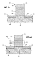
- FIG. 5 is a cross-sectional view of a field effect transistor, including a transistor gate stack in accordance with the present invention.
- FIG. 6 is a cross-sectional view of a field effect transistor, including a transistor gate stack in accordance with the present invention.
- FIG. 7 is a cross-sectional view of a graded interconnect layer disposed on a silicon substrate.
- one or more integrated circuits having one or more graded layers that improve adhesion may be formed on a semiconductor wafer 10 .
- the wafer 10 may be separated into individual integrated circuit dies 11 that may be packaged as integrated circuit chips in any of several well-known packaging configurations.
- Memory chips such as a random access memories (RAMs) or read only memories (ROMs), may be fabricated using the graded layers described herein, although integrated circuits designed to perform a number of electronic circuit functions may also be fabricated using such layers.
- a block diagram of a semiconductor memory 14 is shown generally in FIG. 2 .
- the memory 14 is formed on a semiconductor substrate 16 and contains a memory matrix 18 .
- the memory matrix 18 such as a dynamic random access memory (DRAM) array 24 shown in FIG. 3, is controlled by peripheral circuitry 20 via lines 22 .
- DRAM dynamic random access memory
- FIG. 4 A schematic of a memory cell, and more specifically a DRAM cell 26 , is shown in FIG. 4 .
- the DRAM cell 26 contains an access transistor 28 that controls electrical access to a storage capacitor 34 .
- the access transistor 28 is illustrated as a FET.
- the gate of the access transistor 28 is electrically connected to a word line 30
- the drain of the FET 28 is electrically connected to a bit line 32 .
- the manner in which a DRAM operates is well-known and will not be described further herein.
- FIG. 5 shows a FET 36 , such as that used as the access transistor 28 in the DRAM cell 26 , formed in a silicon substrate 38 .
- a gate stack may be formed in a number of ways, but, in this example, the gate stack is formed by depositing the successive layers one on top of the other and, then, performing a photoresist and etch to define the gate stack. In other words, a dielectric layer of gate oxide 40 is deposited on the substrate 38 .
- a gate layer 48 typically a conductive or semiconductive material such as poiysilicon, is deposited on the gate oxide layer 40 .
- a graded layer 50 is deposited on the gate layer 48 .
- the FET's channel region 42 , source region 44 , and drain 46 region may be formed by etching windows in the gate stack and by doping the silicon substrate 38 in a conventional fashion, such as ion implantation or diffusion.
- the thickness of the gate oxide layer 40 is in the range of 40 ⁇ to 150 ⁇
- the thickness of the gate layer 48 is in the range of 100 ⁇ to 2000 ⁇ .
- the thickness of these layers may be further reduced.
- a graded layer 50 is formed on the gate layer 48 .
- the graded layer 50 transitions from one material to another material.
- the graded layer 50 may be formed from a number of different elements, compounds, or mixtures, including, for example, titanium (Ti), tungsten (W), nitrogen (N), titanium tungsten (TiW), tungsten nitride (WN), titanium nitride (TiN), titanium tungsten nitride (TiWN), titanium aluminum nitride (TiAlN), titanium silicide (TiSi), or titanium silicon nitride (TiSiN). Because WSi is not used, films having lower resistivity may be achieved.
- the composition of the graded layer 50 may be varied from (1) TiW to W, where Ti varies from 0.25% to 99.5% and W varies from 0.25% to 99.5%; (2) WN to W, where N varies from 0.25% to 99.5% and W varies from 0.25% to 99.5%; and (3) TiWN to W, where Ti varies from 0.25% to 99.5%, W varies from 0.25% to 99.5%, and N varies from 0.25% to 99.5%.
- the graded layer 50 may gradually transition from a material comprising a single element, such as tungsten, at the bottom of the graded barrier layer 50 to another material, such as TiW, at the top of the graded layer 50 , or the other way around.
- the graded layer 50 may be made of a number of discrete sub-layers.
- FIG. 6 shows an example of a graded layer 50 formed from three sublayers 50 a, 50 b, and 50 c.
- Each sublayer 50 a, 50 b, and 50 c may have a particular composition, or each sublayer 50 a, 50 b, 50 c may have a graded variation of materials to achieve the desired effect.
- the graded layer 50 is graded from a first material at the portion of the graded layer 50 closest to the gate layer 48 , e.g., the bottom of the graded layer 50 , to a second material at the portion of the graded layer 50 closest to a subsequently formed layer, e.g., the top of the graded layer 50 .
- the bottom of the graded layer 50 may be TiN or TiW
- the top of the graded layer 50 may be pure tungsten.
- the material ratio of constituent compositional elements of the graded layer 50 may vary according to the respective formula Ti x N (1 ⁇ x) or Ti x W (1 ⁇ x) , such that x equals 0.5 at the bottom of the graded layer 50 and x equals 0 at the top of the graded layer 50 .
- the value of x and the manner in which the value of x changes from the bottom to the top of the graded layer 50 may vary depending upon various factors, such as the type of material in layers adjacent the bottom and top of the graded layer 50 .
- the composition of the graded layer 50 is chosen so that its adhesion properties and material stress will be optimized as closely as possible to the adhesion properties and material stress of adjacent layers.
- the graded layer 48 is used as a barrier layer between the gate layer 48 and the interconnect layer 52 in a gate stack
- the material used to form the bottom of the graded layer 50 may be chosen so that its properties are optimized relative to those of the underlying gate layer 48
- the material used to form the top of the graded layer 50 may be chosen so that its properties are optimized relative to those of the overlying conductive interconnect layer 52 .
- a number of different methods may be used to form the graded layer 50 , but sputtering is one particularly useful method of forming the graded layer 50 .
- a single sputtering target may contain the materials used in the graded layer 50 .
- multiple sputtering targets, each containing a different material may be used.
- conventional sputtering techniques may be used to deposit the graded layer 50 .
- Various sputtering machines such as the Eclipse available from Material Research Corporation or the Endura available from Applied Materials, may be utilized to sputter a graded layer of the desired thickness, typically in the range of 50 ⁇ to 20,000 ⁇ .
- a single sputtering target may contain a varying mixture of tungsten and titanium.
- the mixture may vary from a particular TiW compound at the center of the target and change, gradually or abruptly, to a composition of pure tungsten at the target's periphery.
- the TiW compound at the center of the target may be graduated to 100% tungsten at a radial distance of 40% to 60% of the radial length from the center of the target.
- the percentage of tungsten may be varied in a linear or nonlinear fashion from the target's center to its periphery, and the sputtering process may progress from the center of the sputtering target to the target edges in a linear or nonlinear fashion.
- the process for sputtering the graded layer 50 may include a series of successive sputtering steps, each utilizing one of the multiple sputtering targets to achieve the desired gradation within the graded layer 50 .
- the graded layer 50 may also be deposited using chemical vapor deposition (CVD), including PECVD and OMCVD. If CVD is used to create the graded layer 50 , the gas flow, concentration, and/or composition may be varied during the deposition of the graded layer 50 to create the desired compositional grading. For instance, if the desired graded layer 50 transitions from WN to TiWN, then a suitable source, such as an organometallic source, is used for each constituent component Ti, W, and N, and the flow, concentration, and/or composition of each a source may be varied to deposit the desired graded layer 50 .
- CVD chemical vapor deposition
- OMCVD OMCVD
- the gas may initially include tungsten fluoride, ammonia, nitrogen, and argon. The transition is effected by tapering off the flows of ammonia and nitrogen.
- an interconnect layer 52 may be formed on top of the graded layer 50 .
- the interconnect layer 52 may be deposited by conventional techniques, such as sputtering or CVD.
- the interconnect layer 52 couples the transistor's gate to other circuit elements.
- the interconnect layer 52 is typically formed from a conductive material, such as tungsten, and it typically has a thickness of 1000 ⁇ -2000 ⁇ .
- an insulative layer 53 such as a nitride.
- the graded layer 50 may eliminate the need for an overlying conductive interconnect layer, such as the interconnect layer 52 .
- the graded layer 50 may be graded from a tungsten nitride (WN) at its bottom to 100% tungsten, or some other highly conductive material at its top. Because the top portion of the graded layer 50 is highly conductive, the conductive interconnect layer 52 , distinct from the graded barrier layer 50 , may be eliminated.
- WN tungsten nitride
- DRAM bit lines 32 may be formed from a graded interconnect layer deposited on a semiconductor substrate or other underlying structure, using a process such as that described above.
- the graded interconnect layer 56 may be graded from titanium tungsten at the interconnect's interface with the substrate 54 to pure tungsten at the top of the graded interconnect layer 56 .
- the graded interconnect layer 56 will typically be in the range of 50 ⁇ to 20,000 ⁇ , but preferably will be of 8000 ⁇ to 10,000 ⁇ in thickness.
- An insulating layer 57 may be deposited over the top and sides of the interconnect layer 56 .
- a graded interconnect layer 56 as described herein may also be used in a multilevel metalization system in which: a first interconnecting network may be formed; a dielectric layer may be formed on top of the first interconnecting network; and a second interconnecting network may be formed on top of the dielectric layer.
- any of the layers disclosed herein e.g., the gate layer 48 or graded layer 50
Abstract
Description
Claims (14)
Priority Applications (2)
| Application Number | Priority Date | Filing Date | Title |
|---|---|---|---|
| US09/887,612 US6451658B2 (en) | 1998-08-21 | 2001-06-22 | Graded layer for use in semiconductor circuits and method for making same |
| US10/051,768 US6545356B2 (en) | 1998-08-21 | 2002-01-18 | Graded layer for use in semiconductor circuits and method for making same |
Applications Claiming Priority (2)
| Application Number | Priority Date | Filing Date | Title |
|---|---|---|---|
| US09/138,811 US6271590B1 (en) | 1998-08-21 | 1998-08-21 | Graded layer for use in semiconductor circuits and method for making same |
| US09/887,612 US6451658B2 (en) | 1998-08-21 | 2001-06-22 | Graded layer for use in semiconductor circuits and method for making same |
Related Parent Applications (1)
| Application Number | Title | Priority Date | Filing Date |
|---|---|---|---|
| US09/138,811 Division US6271590B1 (en) | 1998-08-21 | 1998-08-21 | Graded layer for use in semiconductor circuits and method for making same |
Related Child Applications (1)
| Application Number | Title | Priority Date | Filing Date |
|---|---|---|---|
| US10/051,768 Division US6545356B2 (en) | 1998-08-21 | 2002-01-18 | Graded layer for use in semiconductor circuits and method for making same |
Publications (2)
| Publication Number | Publication Date |
|---|---|
| US20010033027A1 US20010033027A1 (en) | 2001-10-25 |
| US6451658B2 true US6451658B2 (en) | 2002-09-17 |
Family
ID=22483766
Family Applications (3)
| Application Number | Title | Priority Date | Filing Date |
|---|---|---|---|
| US09/138,811 Expired - Lifetime US6271590B1 (en) | 1998-08-21 | 1998-08-21 | Graded layer for use in semiconductor circuits and method for making same |
| US09/887,612 Expired - Lifetime US6451658B2 (en) | 1998-08-21 | 2001-06-22 | Graded layer for use in semiconductor circuits and method for making same |
| US10/051,768 Expired - Lifetime US6545356B2 (en) | 1998-08-21 | 2002-01-18 | Graded layer for use in semiconductor circuits and method for making same |
Family Applications Before (1)
| Application Number | Title | Priority Date | Filing Date |
|---|---|---|---|
| US09/138,811 Expired - Lifetime US6271590B1 (en) | 1998-08-21 | 1998-08-21 | Graded layer for use in semiconductor circuits and method for making same |
Family Applications After (1)
| Application Number | Title | Priority Date | Filing Date |
|---|---|---|---|
| US10/051,768 Expired - Lifetime US6545356B2 (en) | 1998-08-21 | 2002-01-18 | Graded layer for use in semiconductor circuits and method for making same |
Country Status (1)
| Country | Link |
|---|---|
| US (3) | US6271590B1 (en) |
Cited By (3)
| Publication number | Priority date | Publication date | Assignee | Title |
|---|---|---|---|---|
| US20060022279A1 (en) * | 2002-08-26 | 2006-02-02 | Tran Luan C | Semiconductor constructions |
| US20080042145A1 (en) * | 2006-08-18 | 2008-02-21 | Helmut Hagleitner | Diffusion barrier for light emitting diodes |
| US20140070334A1 (en) * | 2012-04-23 | 2014-03-13 | Globalfoundries | Semiconductor device including graded gate stack, related method and design structure |
Families Citing this family (23)
| Publication number | Priority date | Publication date | Assignee | Title |
|---|---|---|---|---|
| US6271590B1 (en) * | 1998-08-21 | 2001-08-07 | Micron Technology, Inc. | Graded layer for use in semiconductor circuits and method for making same |
| DE10163557B4 (en) * | 2001-12-21 | 2007-12-06 | Forschungszentrum Jülich GmbH | Transistor-based sensor with specially designed gate electrode for high-sensitivity detection of analytes |
| US6982474B2 (en) * | 2002-06-25 | 2006-01-03 | Amberwave Systems Corporation | Reacted conductive gate electrodes |
| AU2003273328A1 (en) * | 2002-09-18 | 2004-04-08 | Infineon Technologies Ag | Nitride and polysilicon interface with titanium layer |
| US6686637B1 (en) | 2002-11-21 | 2004-02-03 | International Business Machines Corporation | Gate structure with independently tailored vertical doping profile |
| DE10255835A1 (en) * | 2002-11-29 | 2004-06-17 | Infineon Technologies Ag | Microelectronic component e.g. FET for high density memory, has low ohmic tungsten nitride barrier layer |
| TWI227914B (en) * | 2003-10-06 | 2005-02-11 | Nanya Technology Corp | A method of gate structure fabrication in semiconductor device |
| DE102004004864B4 (en) * | 2004-01-30 | 2008-09-11 | Qimonda Ag | Method for producing a gate structure and gate structure for a transistor |
| US20060197089A1 (en) * | 2005-03-03 | 2006-09-07 | Chunghwa Picture Tubes., Ltd. | Semiconductor device and its manufacturing method |
| US7510966B2 (en) * | 2005-03-07 | 2009-03-31 | Micron Technology, Inc. | Electrically conductive line, method of forming an electrically conductive line, and method of reducing titanium silicide agglomeration in fabrication of titanium silicide over polysilicon transistor gate lines |
| CN100414715C (en) * | 2005-05-08 | 2008-08-27 | 中华映管股份有限公司 | Thin film transistor and its forming method |
| JP2007081189A (en) * | 2005-09-15 | 2007-03-29 | Elpida Memory Inc | Semiconductor storage device and method of manufacturing same |
| DE102007045074B4 (en) | 2006-12-27 | 2009-06-18 | Hynix Semiconductor Inc., Ichon | Semiconductor device with gate stack structure |
| KR100844940B1 (en) * | 2006-12-27 | 2008-07-09 | 주식회사 하이닉스반도체 | Semiconductor device with multi layer diffusion barrier and method for fabricating the same |
| US7781333B2 (en) * | 2006-12-27 | 2010-08-24 | Hynix Semiconductor Inc. | Semiconductor device with gate structure and method for fabricating the semiconductor device |
| US8753936B2 (en) | 2008-08-12 | 2014-06-17 | International Business Machines Corporation | Changing effective work function using ion implantation during dual work function metal gate integration |
| JP5937297B2 (en) * | 2010-03-01 | 2016-06-22 | キヤノンアネルバ株式会社 | Metal nitride film, semiconductor device using the metal nitride film, and method for manufacturing the semiconductor device |
| FR2977367A1 (en) * | 2011-06-30 | 2013-01-04 | St Microelectronics Crolles 2 | TRANSISTORS INCLUDING THE GRID COMPRISING A TITANIUM NITRIDE LAYER AND METHOD FOR DEPOSITING THE SAME |
| US9263556B2 (en) * | 2012-06-29 | 2016-02-16 | Taiwan Semiconductor Manufacturing Company, Ltd. | Silicide process using OD spacers |
| US9401279B2 (en) | 2013-06-14 | 2016-07-26 | Sandisk Technologies Llc | Transistor gate and process for making transistor gate |
| CN110391231B (en) * | 2018-04-16 | 2020-09-22 | 联华电子股份有限公司 | Semiconductor element and manufacturing method thereof |
| CN110391247B (en) * | 2018-04-17 | 2020-10-30 | 联华电子股份有限公司 | Semiconductor element and manufacturing method thereof |
| CN110391233B (en) * | 2018-04-17 | 2022-10-14 | 联华电子股份有限公司 | Semiconductor element and manufacturing method thereof |
Citations (9)
| Publication number | Priority date | Publication date | Assignee | Title |
|---|---|---|---|---|
| US5341016A (en) * | 1993-06-16 | 1994-08-23 | Micron Semiconductor, Inc. | Low resistance device element and interconnection structure |
| US5349205A (en) | 1991-12-02 | 1994-09-20 | Matsushita Electric Industrial Co., Ltd. | Thin-film transistor array with anodic oxide for use in a liquid crystal display |
| US5563449A (en) | 1995-01-19 | 1996-10-08 | Cornell Research Foundation, Inc. | Interconnect structures using group VIII metals |
| US5675186A (en) | 1994-05-31 | 1997-10-07 | Advanced Micro Devices, Inc. | Construction that prevents the undercut of interconnect lines in plasma metal etch systems |
| US5763948A (en) | 1994-09-22 | 1998-06-09 | Sony Corporation | Semiconductor apparatus including a tin barrier layer having a (III) crystal lattice direction |
| US5804878A (en) | 1992-12-09 | 1998-09-08 | Semiconductor Energy Laboratory Co., Ltd. | Electronic circuit |
| US6005277A (en) | 1996-07-15 | 1999-12-21 | Taiwan Semiconductor Manufacturing Company, Ltd. | ARC layer enhancement for reducing metal loss during via etch |
| US6057603A (en) | 1998-07-30 | 2000-05-02 | Advanced Micro Devices, Inc. | Fabrication of integrated circuit inter-level dielectrics using a stop-on-metal dielectric polish process |
| US6271590B1 (en) * | 1998-08-21 | 2001-08-07 | Micron Technology, Inc. | Graded layer for use in semiconductor circuits and method for making same |
Family Cites Families (1)
| Publication number | Priority date | Publication date | Assignee | Title |
|---|---|---|---|---|
| US6168873B1 (en) * | 1997-05-29 | 2001-01-02 | Canon Kabushiki Kaisha | Electrode substrate and recording medium |
-
1998
- 1998-08-21 US US09/138,811 patent/US6271590B1/en not_active Expired - Lifetime
-
2001
- 2001-06-22 US US09/887,612 patent/US6451658B2/en not_active Expired - Lifetime
-
2002
- 2002-01-18 US US10/051,768 patent/US6545356B2/en not_active Expired - Lifetime
Patent Citations (9)
| Publication number | Priority date | Publication date | Assignee | Title |
|---|---|---|---|---|
| US5349205A (en) | 1991-12-02 | 1994-09-20 | Matsushita Electric Industrial Co., Ltd. | Thin-film transistor array with anodic oxide for use in a liquid crystal display |
| US5804878A (en) | 1992-12-09 | 1998-09-08 | Semiconductor Energy Laboratory Co., Ltd. | Electronic circuit |
| US5341016A (en) * | 1993-06-16 | 1994-08-23 | Micron Semiconductor, Inc. | Low resistance device element and interconnection structure |
| US5675186A (en) | 1994-05-31 | 1997-10-07 | Advanced Micro Devices, Inc. | Construction that prevents the undercut of interconnect lines in plasma metal etch systems |
| US5763948A (en) | 1994-09-22 | 1998-06-09 | Sony Corporation | Semiconductor apparatus including a tin barrier layer having a (III) crystal lattice direction |
| US5563449A (en) | 1995-01-19 | 1996-10-08 | Cornell Research Foundation, Inc. | Interconnect structures using group VIII metals |
| US6005277A (en) | 1996-07-15 | 1999-12-21 | Taiwan Semiconductor Manufacturing Company, Ltd. | ARC layer enhancement for reducing metal loss during via etch |
| US6057603A (en) | 1998-07-30 | 2000-05-02 | Advanced Micro Devices, Inc. | Fabrication of integrated circuit inter-level dielectrics using a stop-on-metal dielectric polish process |
| US6271590B1 (en) * | 1998-08-21 | 2001-08-07 | Micron Technology, Inc. | Graded layer for use in semiconductor circuits and method for making same |
Cited By (4)
| Publication number | Priority date | Publication date | Assignee | Title |
|---|---|---|---|---|
| US20060022279A1 (en) * | 2002-08-26 | 2006-02-02 | Tran Luan C | Semiconductor constructions |
| US20080042145A1 (en) * | 2006-08-18 | 2008-02-21 | Helmut Hagleitner | Diffusion barrier for light emitting diodes |
| US20140070334A1 (en) * | 2012-04-23 | 2014-03-13 | Globalfoundries | Semiconductor device including graded gate stack, related method and design structure |
| US9257519B2 (en) * | 2012-04-23 | 2016-02-09 | GlobalFoundries, Inc. | Semiconductor device including graded gate stack, related method and design structure |
Also Published As
| Publication number | Publication date |
|---|---|
| US20020094652A1 (en) | 2002-07-18 |
| US6545356B2 (en) | 2003-04-08 |
| US6271590B1 (en) | 2001-08-07 |
| US20010033027A1 (en) | 2001-10-25 |
Similar Documents
| Publication | Publication Date | Title |
|---|---|---|
| US6451658B2 (en) | Graded layer for use in semiconductor circuits and method for making same | |
| US5341016A (en) | Low resistance device element and interconnection structure | |
| US5162262A (en) | Multi-layered interconnection structure for a semiconductor device and manufactured method thereof | |
| US5049975A (en) | Multi-layered interconnection structure for a semiconductor device | |
| US5710454A (en) | Tungsten silicide polycide gate electrode formed through stacked amorphous silicon (SAS) multi-layer structure. | |
| US5892281A (en) | Tantalum-aluminum-nitrogen material for semiconductor devices | |
| US5614437A (en) | Method for fabricating reliable metallization with Ta-Si-N barrier for semiconductors | |
| US6340629B1 (en) | Method for forming gate electrodes of semiconductor device using a separated WN layer | |
| US6184550B1 (en) | Ternary nitride-carbide barrier layers | |
| US4886764A (en) | Process for making refractory metal silicide cap for protecting multi-layer polycide structure | |
| US6750500B1 (en) | Capacitor electrode for integrating high K materials | |
| US5869901A (en) | Semiconductor device having aluminum interconnection and method of manufacturing the same | |
| US5918118A (en) | Dual deposition methods for forming contact metallizations, capacitors, and memory devices | |
| US6162671A (en) | Method of forming capacitors having high dielectric constant material | |
| US7875939B2 (en) | Semiconductor device including an ohmic layer | |
| US6140231A (en) | Robust diffusion barrier for Cu metallization | |
| US6552431B2 (en) | Semiconductor structure with a titanium aluminum nitride layer and method for fabricating same | |
| US5604382A (en) | Semiconductor device with pillar-shaped contact layer | |
| JP2002231723A (en) | Barrier layer for copper coating in manufacture of integrated circuit | |
| KR100499429B1 (en) | Microelectronic structure, production method and utilization of the same | |
| US6528835B1 (en) | Titanium nitride metal interconnection system and method of forming the same | |
| US6011289A (en) | Metal oxide stack for flash memory application | |
| US6054771A (en) | Interconnection system in a semiconductor device | |
| US20040150108A1 (en) | Low resistance barrier for a microelectronic component and method for fabricating the same | |
| JP2000183349A (en) | Manufacture of silicon fet |
Legal Events
| Date | Code | Title | Description |
|---|---|---|---|
| STCF | Information on status: patent grant |
Free format text: PATENTED CASE |
|
| FPAY | Fee payment |
Year of fee payment: 4 |
|
| AS | Assignment |
Owner name: MOSAID TECHNOLOGIES INCORPORATED, CANADA Free format text: ASSIGNMENT OF ASSIGNORS INTEREST;ASSIGNOR:MICRON TECHNOLOGY, INC.;REEL/FRAME:023220/0243 Effective date: 20090609 |
|
| FPAY | Fee payment |
Year of fee payment: 8 |
|
| AS | Assignment |
Owner name: MOSAID TECHNOLOGIES INCORPORATED,CANADA Free format text: CORRECTIVE ASSIGNMENT TO CORRECT THE TO CORRECT THE ASSIGNEES' ADDRESS PREVIOUSLY RECORDED ON REEL 023220 FRAME 0243. ASSIGNOR(S) HEREBY CONFIRMS THE MOSAID TECHNOLOGIES INCORPORATED 6 SAUBLE DRIVE, SUITE 203, OTTAWA,ONTARIO, CANADA K2K 2X1;ASSIGNOR:MICRON TECHNOLOGY, INC.;REEL/FRAME:024225/0878 Effective date: 20090609 |
|
| AS | Assignment |
Owner name: ROYAL BANK OF CANADA, CANADA Free format text: U.S. INTELLECTUAL PROPERTY SECURITY AGREEMENT (FOR NON-U.S. GRANTORS) - SHORT FORM;ASSIGNORS:658276 N.B. LTD.;658868 N.B. INC.;MOSAID TECHNOLOGIES INCORPORATED;REEL/FRAME:027512/0196 Effective date: 20111223 |
|
| AS | Assignment |
Owner name: CONVERSANT INTELLECTUAL PROPERTY MANAGEMENT INC., Free format text: CHANGE OF NAME;ASSIGNOR:MOSAID TECHNOLOGIES INCORPORATED;REEL/FRAME:032439/0638 Effective date: 20140101 |
|
| FPAY | Fee payment |
Year of fee payment: 12 |
|
| AS | Assignment |
Owner name: CONVERSANT INTELLECTUAL PROPERTY MANAGEMENT INC., Free format text: RELEASE OF SECURITY INTEREST;ASSIGNOR:ROYAL BANK OF CANADA;REEL/FRAME:033484/0344 Effective date: 20140611 Owner name: CONVERSANT IP N.B. 868 INC., CANADA Free format text: RELEASE OF SECURITY INTEREST;ASSIGNOR:ROYAL BANK OF CANADA;REEL/FRAME:033484/0344 Effective date: 20140611 Owner name: CONVERSANT IP N.B. 276 INC., CANADA Free format text: RELEASE OF SECURITY INTEREST;ASSIGNOR:ROYAL BANK OF CANADA;REEL/FRAME:033484/0344 Effective date: 20140611 |
|
| AS | Assignment |
Owner name: CONVERSANT INTELLECTUAL PROPERTY MANAGEMENT INC., CANADA Free format text: CHANGE OF ADDRESS;ASSIGNOR:CONVERSANT INTELLECTUAL PROPERTY MANAGEMENT INC.;REEL/FRAME:033678/0096 Effective date: 20140820 Owner name: CONVERSANT INTELLECTUAL PROPERTY MANAGEMENT INC., Free format text: CHANGE OF ADDRESS;ASSIGNOR:CONVERSANT INTELLECTUAL PROPERTY MANAGEMENT INC.;REEL/FRAME:033678/0096 Effective date: 20140820 |
|
| AS | Assignment |
Owner name: CPPIB CREDIT INVESTMENTS INC., AS LENDER, CANADA Free format text: U.S. PATENT SECURITY AGREEMENT (FOR NON-U.S. GRANTORS);ASSIGNOR:CONVERSANT INTELLECTUAL PROPERTY MANAGEMENT INC.;REEL/FRAME:033706/0367 Effective date: 20140611 Owner name: ROYAL BANK OF CANADA, AS LENDER, CANADA Free format text: U.S. PATENT SECURITY AGREEMENT (FOR NON-U.S. GRANTORS);ASSIGNOR:CONVERSANT INTELLECTUAL PROPERTY MANAGEMENT INC.;REEL/FRAME:033706/0367 Effective date: 20140611 |
|
| AS | Assignment |
Owner name: CPPIB CREDIT INVESTMENTS, INC., CANADA Free format text: AMENDED AND RESTATED U.S. PATENT SECURITY AGREEMENT (FOR NON-U.S. GRANTORS);ASSIGNOR:CONVERSANT INTELLECTUAL PROPERTY MANAGEMENT INC.;REEL/FRAME:046900/0136 Effective date: 20180731 |
|
| AS | Assignment |
Owner name: CONVERSANT INTELLECTUAL PROPERTY MANAGEMENT INC., CANADA Free format text: RELEASE OF U.S. PATENT AGREEMENT (FOR NON-U.S. GRANTORS);ASSIGNOR:ROYAL BANK OF CANADA, AS LENDER;REEL/FRAME:047645/0424 Effective date: 20180731 Owner name: CONVERSANT INTELLECTUAL PROPERTY MANAGEMENT INC., Free format text: RELEASE OF U.S. PATENT AGREEMENT (FOR NON-U.S. GRANTORS);ASSIGNOR:ROYAL BANK OF CANADA, AS LENDER;REEL/FRAME:047645/0424 Effective date: 20180731 |
|
| AS | Assignment |
Owner name: CONVERSANT INTELLECTUAL PROPERTY MANAGEMENT INC., CANADA Free format text: RELEASE BY SECURED PARTY;ASSIGNOR:CPPIB CREDIT INVESTMENTS INC.;REEL/FRAME:054372/0281 Effective date: 20201028 |