US6452427B1 - Dual output capacitance interface circuit - Google Patents

Dual output capacitance interface circuit Download PDF

Info

Publication number
US6452427B1
US6452427B1 US09/743,525 US74352501A US6452427B1 US 6452427 B1 US6452427 B1 US 6452427B1 US 74352501 A US74352501 A US 74352501A US 6452427 B1 US6452427 B1 US 6452427B1
Authority
US
United States
Prior art keywords
current
capacitance
converter
output
voltage
Prior art date
Legal status (The legal status is an assumption and is not a legal conclusion. Google has not performed a legal analysis and makes no representation as to the accuracy of the status listed.)
Expired - Fee Related
Application number
US09/743,525
Inventor
Wen H. Ko
Qiang Wang
Current Assignee (The listed assignees may be inaccurate. Google has not performed a legal analysis and makes no representation or warranty as to the accuracy of the list.)
Case Western Reserve University
Original Assignee
Wen H. Ko
Qiang Wang
Priority date (The priority date is an assumption and is not a legal conclusion. Google has not performed a legal analysis and makes no representation as to the accuracy of the date listed.)
Filing date
Publication date
Application filed by Wen H. Ko, Qiang Wang filed Critical Wen H. Ko
Priority to US09/743,525 priority Critical patent/US6452427B1/en
Application granted granted Critical
Publication of US6452427B1 publication Critical patent/US6452427B1/en
Assigned to JPMORGAN CHASE BANK reassignment JPMORGAN CHASE BANK THE MASTER GUARANTEE AND COLLATERIAL AGREEMENT Assignors: GOODYEAR TIRE & RUBBER COMPANY, THE
Assigned to THE GOODYEAR TIRE & RUBBER COMPANY reassignment THE GOODYEAR TIRE & RUBBER COMPANY RELEASE BY SECURED PARTY (SEE DOCUMENT FOR DETAILS). Assignors: JPMORGAN CHASE BANK, N.A.
Assigned to CASE WESTERN RESERVE UNIVERSITY reassignment CASE WESTERN RESERVE UNIVERSITY ASSIGNMENT OF ASSIGNORS INTEREST (SEE DOCUMENT FOR DETAILS). Assignors: THE GOODYEAR TIRE & RUBBER COMPANY
Anticipated expiration legal-status Critical
Expired - Fee Related legal-status Critical Current

Links

Images

Classifications

    • GPHYSICS
    • G01MEASURING; TESTING
    • G01DMEASURING NOT SPECIALLY ADAPTED FOR A SPECIFIC VARIABLE; ARRANGEMENTS FOR MEASURING TWO OR MORE VARIABLES NOT COVERED IN A SINGLE OTHER SUBCLASS; TARIFF METERING APPARATUS; MEASURING OR TESTING NOT OTHERWISE PROVIDED FOR
    • G01D5/00Mechanical means for transferring the output of a sensing member; Means for converting the output of a sensing member to another variable where the form or nature of the sensing member does not constrain the means for converting; Transducers not specially adapted for a specific variable
    • G01D5/12Mechanical means for transferring the output of a sensing member; Means for converting the output of a sensing member to another variable where the form or nature of the sensing member does not constrain the means for converting; Transducers not specially adapted for a specific variable using electric or magnetic means
    • G01D5/14Mechanical means for transferring the output of a sensing member; Means for converting the output of a sensing member to another variable where the form or nature of the sensing member does not constrain the means for converting; Transducers not specially adapted for a specific variable using electric or magnetic means influencing the magnitude of a current or voltage
    • G01D5/24Mechanical means for transferring the output of a sensing member; Means for converting the output of a sensing member to another variable where the form or nature of the sensing member does not constrain the means for converting; Transducers not specially adapted for a specific variable using electric or magnetic means influencing the magnitude of a current or voltage by varying capacitance
    • G01D5/241Mechanical means for transferring the output of a sensing member; Means for converting the output of a sensing member to another variable where the form or nature of the sensing member does not constrain the means for converting; Transducers not specially adapted for a specific variable using electric or magnetic means influencing the magnitude of a current or voltage by varying capacitance by relative movement of capacitor electrodes
    • G01D5/2417Mechanical means for transferring the output of a sensing member; Means for converting the output of a sensing member to another variable where the form or nature of the sensing member does not constrain the means for converting; Transducers not specially adapted for a specific variable using electric or magnetic means influencing the magnitude of a current or voltage by varying capacitance by relative movement of capacitor electrodes by varying separation
    • GPHYSICS
    • G01MEASURING; TESTING
    • G01LMEASURING FORCE, STRESS, TORQUE, WORK, MECHANICAL POWER, MECHANICAL EFFICIENCY, OR FLUID PRESSURE
    • G01L17/00Devices or apparatus for measuring tyre pressure or the pressure in other inflated bodies
    • GPHYSICS
    • G01MEASURING; TESTING
    • G01LMEASURING FORCE, STRESS, TORQUE, WORK, MECHANICAL POWER, MECHANICAL EFFICIENCY, OR FLUID PRESSURE
    • G01L9/00Measuring steady of quasi-steady pressure of fluid or fluent solid material by electric or magnetic pressure-sensitive elements; Transmitting or indicating the displacement of mechanical pressure-sensitive elements, used to measure the steady or quasi-steady pressure of a fluid or fluent solid material, by electric or magnetic means
    • G01L9/0041Transmitting or indicating the displacement of flexible diaphragms
    • G01L9/0042Constructional details associated with semiconductive diaphragm sensors, e.g. etching, or constructional details of non-semiconductive diaphragms
    • GPHYSICS
    • G01MEASURING; TESTING
    • G01LMEASURING FORCE, STRESS, TORQUE, WORK, MECHANICAL POWER, MECHANICAL EFFICIENCY, OR FLUID PRESSURE
    • G01L9/00Measuring steady of quasi-steady pressure of fluid or fluent solid material by electric or magnetic pressure-sensitive elements; Transmitting or indicating the displacement of mechanical pressure-sensitive elements, used to measure the steady or quasi-steady pressure of a fluid or fluent solid material, by electric or magnetic means
    • G01L9/0041Transmitting or indicating the displacement of flexible diaphragms
    • G01L9/0072Transmitting or indicating the displacement of flexible diaphragms using variations in capacitance
    • G01L9/0073Transmitting or indicating the displacement of flexible diaphragms using variations in capacitance using a semiconductive diaphragm
    • GPHYSICS
    • G01MEASURING; TESTING
    • G01LMEASURING FORCE, STRESS, TORQUE, WORK, MECHANICAL POWER, MECHANICAL EFFICIENCY, OR FLUID PRESSURE
    • G01L9/00Measuring steady of quasi-steady pressure of fluid or fluent solid material by electric or magnetic pressure-sensitive elements; Transmitting or indicating the displacement of mechanical pressure-sensitive elements, used to measure the steady or quasi-steady pressure of a fluid or fluent solid material, by electric or magnetic means
    • G01L9/12Measuring steady of quasi-steady pressure of fluid or fluent solid material by electric or magnetic pressure-sensitive elements; Transmitting or indicating the displacement of mechanical pressure-sensitive elements, used to measure the steady or quasi-steady pressure of a fluid or fluent solid material, by electric or magnetic means by making use of variations in capacitance, i.e. electric circuits therefor
    • G01L9/125Measuring steady of quasi-steady pressure of fluid or fluent solid material by electric or magnetic pressure-sensitive elements; Transmitting or indicating the displacement of mechanical pressure-sensitive elements, used to measure the steady or quasi-steady pressure of a fluid or fluent solid material, by electric or magnetic means by making use of variations in capacitance, i.e. electric circuits therefor with temperature compensating means

Definitions

  • the invention relates to circuits for interfacing with and deriving usable signals from transducers, more particularly capacitive force transducers such as pressure transducers, more particularly touch mode capacitive pressure sensors (“TMCPS”).
  • transducers more particularly capacitive force transducers such as pressure transducers, more particularly touch mode capacitive pressure sensors (“TMCPS”).
  • TCPS touch mode capacitive pressure sensors
  • Capacitive pressure sensors typically include a pair of conductive elements, one of which is a fixed substrate another of which is a flexible diaphragm.
  • a capacitive pressure sensor As pressure increases a gap between the diaphragm and the underlying substrate decreases, and the capacitance of the sensor increases.
  • the sensor is normally operated in a pressure range wherein the diaphragm is kept from actually contacting the underlying substrate.
  • These sensors normally exhibit nonlinear characteristics. This inherent non-linearity has led to the development of many linearization schemes using complex and costly interface circuits which include analog circuits and amplifiers, segment linearization, microprocessor and ROM matrix linearization, etc.
  • TCPS touch mode capacitive pressure sensor
  • touch mode operation the diaphragm of the capacitive pressure sensor touches the underlying substrate which is covered by a thin insulating layer. As pressure increases, the contact area increases.
  • the major component of output capacitance is the capacitance of the touched area with a thin layer of isolation layer which gives a larger capacitance per unit area compared to the air-gap capacitance in the untouched area.
  • the touch mode device was developed to withstand harsh industrial environment, and with one or two orders of magnitude higher sensitivity than the normal (non-touch) mode operation in the near linear operation range, so that some of the stray capacity effects can be neglected.
  • touch mode capacitive pressure sensors include near linear output characteristics, large over-range pressure capability and robust structure that make them capable to withstand harsh industrial field environments.
  • One application of interest for pressure sensors generally, and touch mode capacitive pressure sensors in particular, is in conjunction with an RF transponder inside a pneumatic tire.
  • TMCPS touch mode capacitive pressure sensors
  • SFBCPS silicon fusion bonded capacitive pressure sensor
  • FIG. 8 shows the outline of major steps of the fabrication of SFBCPS.
  • Two silicon wafers are needed to make silicon fusion bonded capacitive pressure sensors.
  • wafer A cavities are formed by silicon etching to define the gap.
  • the bottom electrode on wafer A is formed by boron diffusion on the bottom of the cavity.
  • a capacitive absolute pressure sensor needs an electrode feedthrough from a hermetically sealed cavity.
  • the electrode feedthrough is lain down in a groove in the feedthrough region. (The groove is sealed after the bonding and etching processes).
  • the isolation between two electrodes of the sensor is realized by the thermal oxide on the bonding surface. Due to doping concentration dependent oxidation, there is usually a step generated in the feedthrough region if the feedthrough electrode is on the surface.
  • the process discussed before can be simplified to a three-layer process.
  • the structure of the fabricated sensor is illustrated in FIG. 10.
  • the substrate as whole will be used as the bottom electrode.
  • the gap is defined by the thickness of thermally grown oxide. Since there is no electrode feedthrough required, the hermetically sealed reference cavity can be formed by silicon to silicon fusion bonding without introducing extra processes.
  • the sensor chip is 1.0 mm ⁇ 1.5 mm ⁇ 0.4 mm in size.
  • the diaphragm sizes range from 300 to 400 (mn in diameters.
  • the process starts with the P-type substrate silicon wafer with 2.2-(m thermally grown oxide.
  • the thickness of the oxide determines the initial gap of the capacitive pressure sensor.
  • the oxide in cavity area is etched using RIE, which can give very vertical sidewall after etching.
  • the same thickness of oxide on the backside wafer can be used not only as wet silicon etch mask, but also compensates the stress in the front side oxide so that the wafer can keep flat for the silicon fusion bonding.
  • a 0.1-(m thick oxide is grown for the electrical isolation after the diaphragm touches the bottom.
  • the top silicon wafer with a well-defined thickness of heavily doped boron is then bonded to the cavity patterned substrate wafer using silicon fusion bond technique. No alignment is required during the bonding.
  • the Si—Si “wafer” is immersed in a dopant-dependent etchant (such as EDP, KOH and TMAH) to dissolve the silicon of the top wafer except the P+ layer.
  • a dopant-dependent etchant such as EDP, KOH and TMAH
  • the P+ layer is then patterned to form the two capacitors and open the substrate contact window.
  • Al contact pads are formed in the end using lift-off technique. This process utilizes single-side processing of silicon wafers. It only requires three non-critical masking steps and can produce very high yield.”
  • the large zero-pressure capacitance originates from the large bonding area and the isolation material with a large dielectric constant surrounding the diaphragm. At zero-pressure, since the deflection of the diaphragm is small, the gap distance between diaphragm and the electrode on the bottom electrode is large. Therefore the capacitance of the air-gap capacitor contributes a small part to the overall capacitance at zero-pressure.
  • the zero-pressure capacitance is mainly determined by the bonding area required to ensure the hermetic seal and mechanically support of the diaphragm. In the current design, the measured zero-pressure capacitance of the fabricated sensor is 7.3 pF, of which the bonding area contributes about 80%.
  • U.S. Pat. No. 4,104,595 discloses a signal translating circuit for variable area capacitive pressure transducer.
  • the circuit translates the capacitance change of a variable area capacitive transducer into a d-c voltage change.
  • the transducer has two electrodes. As a force is applied to a deformable one of two electrodes, there is a change in the effective contact area between the electrodes in accordance with the applied pressure, producing a resulting change in capacitance.
  • the signal translating circuit produces a d-c output signal which varies as a function of the transducer capacitance change.
  • U.S. Pat. No. 4,446,447 discloses a circuit for converting pressure variation to frequency variation which includes a reference oscillator and a sensor oscillator coupled to a digital mixer.
  • the reference oscillator includes a reference capacitor and a reference resistor.
  • the sensor oscillator has a variable sensor timing capacitor and a sensor resistor.
  • transducers more particularly capacitive force transducers such as pressure transducers, more particularly touch mode capacitive pressure sensors (“TMCPS”), as defined in one or more of the appended claims and, as such, having the capability of being implemented in a manner to accomplish one or more of the subsidiary objects.
  • a dual output capacitance interface circuit ( 100 , FIG. 1) provides a voltage output ( 104 ) and a frequency output ( 106 ), each of which is related to a capacitance value of a condition-sensitive capacitance (Cx), such as a touch-mode capacitive pressure sensor.
  • a capacitance-to-current (C-I) sub-circuit 110 converts capacitance to current.
  • a current-to-frequency (I-F) sub-circuit ( 112 ) converts current to frequency signal.
  • a current-to-voltage (I-V) sub-circuit ( 114 ) converts current to a DC voltage.
  • the capacitance-to-current (C-I) converter comprises three capacitor controlled current sources controlled by a three-phase non-overlapping clock ( 116 , FIG. 9 ).
  • the three-phase non-overlapping clock (FIG. 9) may be driven by a clock generator (FIG. 10) comprising a Schmitt trigger.
  • the current-to-frequency (I-F) converter ( 112 , FIG. 5A) comprises a Schmitt trigger.
  • the circuit is programmable independently with sensitivity and offset adjustment, and is insensitive to fixed stray capacitance.
  • the dual output capacitance interface circuit ( 100 ) is based on switched capacitor circuits and charge subtraction techniques for providing the voltage ( 104 ) and frequency ( 106 ) outputs.
  • the circuit is programmable independently with sensitivity and offset adjustment, and is insensitive to fixed stray capacitance. Temperature compensation methods are described.
  • similar elements may be referred to with similar numbers in a single FIGURE.
  • a plurality of elements 199 may be referred to as 199 a 199 b , 199 c , etc.
  • cross-sectional views, if any, presented herein may be in the form of “slices”, or “near-sighted” cross-sectional views, omitting certain background lines which would otherwise be visible in a true cross-sectional view, for illustrative clarity.
  • FIG. 1 is a block diagram of an embodiment of a Dual Output Capacitance Interface Circuit (“interface circuit”), according to the invention
  • FIGS. 2, 3 and 4 are simplified schematics illustrating the operation and an implementation of a capacitance-to-current converter sub-circuit of the interface circuit illustrated in FIG. 1, according to the invention
  • FIG. 5A is a simplified schematics illustrating the operation and an implementation of a current-to-frequency (I-F) converter sub-circuit of the interface circuit illustrated in FIG. 1, according to the invention
  • FIG. 5B is a wave form diagram for the current-to-frequency converter, according to the invention.
  • FIG. 6 is a schematic for a configuration of a CMOS Schmitt trigger circuit, according to the invention.
  • FIG. 7 is a state diagram of a three-phase clock generator sub-circuit of the interface circuit illustrated in FIG. 1, according to the invention.
  • FIG. 8 is a true value table for the three-phase clock generator sub-circuit of the interface circuit illustrated in FIG. 1, according to the invention.
  • FIG. 9 is a schematic of an implementation of the three-phase clock generator sub-circuit of the interface circuit illustrated in FIG. 1, according to the invention.
  • FIG. 10 is a schematic of a Schmitt oscillator (input clock generator) for providing a high duty cycle pulse for the three-phase clock generator sub-circuit of FIG. 9, according to the invention
  • FIG. 11 is a timing diagram for the three-phase clock generator sub-circuit of FIG. 9 and the Schmitt oscillator of FIG. 10, according to the invention.
  • FIG. 12 is a graph showing a Pspice-simulated resolution of a C-F converter, according to the invention.
  • FIG. 13 is a graph showing a Pspice-simulated temperature characteristic of a threshold voltage for a Schmitt trigger, according to the invention.
  • FIG. 15 is a simplified schematic of a modified clock generator with temperature compensation, according to the invention.
  • FIG. 16 is a graph showing a Pspice-simulated temperature characteristic of a clock generator with temperature compensation, according to the invention.
  • FIG. 17 is a graph showing temperature characteristics of a C-F converter without temperature compensation, according to the invention.
  • FIG. 18A is a simplified schematic showing a current difference-to-voltage converter, according to the invention.
  • FIG. 18B is simplified schematic of a small signal equivalent circuit for a current difference-to-voltage converter, according to the invention.
  • FIG. 19 is a simplified schematic of a reference current generator for a current difference-to-voltage converter, according to the invention.
  • FIG. 20 is a graph illustrating characteristics of the dual output converter of the present invention.
  • FIG. 1 is a block diagram of an embodiment of the Dual Output Capacitance Interface Circuit (“interface circuit”) 100 of the present invention.
  • the circuit 100 has an input 102 , to which is connected a variable capacitance (Cx), and has two outputs—a voltage output 104 and a frequency output 106 , both of which vary according to the value of the capacitance (Cx) on the input 102 of the interface circuit 100 .
  • the interface circuit 100 comprises four major functional blocks (sub-circuits):
  • C-I converter 110 capacitance-to-current converter 110 (capacitor-controlled current source) which converts the measured capacitance (Cx) to a current signal;
  • I-F current-to-frequency
  • I-V converter 114 (followed by a buffer 115 ) which is used to convert the current from the C-I converter 110 to a DC voltage signal on the output 104 ;
  • a three-phase clock generator 116 driven by an oscillator 118 controlled by a capacitor (Cosc), which provides a three-phase non-overlapping clock to control the charging/discharging process of the capacitance-to-current (C-I) converter 110 .
  • No reset is necessary to initiate the three-phase clock.
  • the transition of the states is designed to avoid any simultaneous high state of the three phases.
  • FIGS. 2, 3 and 4 are simplified schematics illustrating the operation and an implementation of the capacitance-to-current (C-I) converter 110 of FIG. 1 .
  • a modified switched-capacitor emulated resistor may be used to implement the capacitor controlled current source, and is shown in FIG. 2 .
  • Switches S 1 and S 2 are controlled by a non-overlapping two-phase clock (not shown).
  • phase 1 switch S 1 is closed and switch S 2 is opened.
  • the capacitor, C is charged to V 1 at the end of phase 1.
  • the charge on the capacitor C is CV 1
  • phase 2 the switch S 1 is opened and the switch S 2 is closed.
  • the net charge transferred in one clock cycle is CV 1 ⁇ CV 2 .
  • the equivalent resistance between V 1 and V 2 is 1/ ⁇ C.
  • the capacitance-to-current (C-I) converter 110 can be constructed by three capacitor controlled current sources as shown in FIG. 4 .
  • the circuit is controlled by a three-phase non-overlapping clock ( 116 ).
  • switches S 1 and S 2 are closed.
  • Capacitors C x and C o are charged to voltages V g and V o , respectively.
  • the switches S 3 and S 4 are closed.
  • the charge in the capacitor C o is discharged through the transistor M 1 .
  • the same amount of charge will be drawn from the capacitor C x through the transistor M 2 in the same time period when the capacitor C o is discharged, providing that the transistor M 2 remains saturated.
  • K 1 ⁇ (V g ⁇ V T )
  • K 2 ⁇ (V o ⁇ V T )
  • K 3 ⁇ (V o ⁇ V T )C o , assuming that threshold voltages of the transistors M 1 , M 2 and M 3 are the same.
  • the current I, flowing through the transistor. M 3 is related to (a measure of) the capacitance C x .
  • the current I is also related to both ⁇ V g and ⁇ V o C o , which makes it possible to adjust the current by two external parameters, V g and V o C o , independently.
  • the V o C o is used to adjust reference or offset current, while V g is used for gain control of C-I converter 110 .
  • FIGS. 5A, 5 B and 6 illustrate the operation and an implementation of the current-to-frequency (I-F) converter 112 of FIG. 1 .
  • FIG. 5A is a simplified schematic illustrating the operation and an implementation of the current-to-frequency (I-F) converter 112 of FIG. 1 .
  • An output portion of the C-I converter 110 including the transistors M 3 and M 4 is shown to the left of a dashed line.
  • the current-to-frequency (I-F) components are shown to the right of the dashed line.
  • a Schmitt trigger is used to implement current-to-frequency (I-F) conversion.
  • the Schmitt trigger has two trigger points, i.e., high threshold voltage, V H , and low threshold voltage, V L . If the input voltage of a Schmitt trigger varies from low to high, the output voltage will change from high to low when the input reaches the high threshold voltage. If the input voltage varies from high to low, the output voltage will change from low to high when the input reaches the low threshold voltage.
  • the input voltage of the Schmitt trigger in the I-F converter is the voltage on a capacitor, C st , which is charged by a current source. Using average current I in equation Eqn.
  • a symmetric square wave can be obtained from the output of the Schmitt trigger, as shown in the graphs of FIG. 5 B.
  • the charge current source and the discharge sink can be realized by two current mirrors controlled by two switches, as shown in FIG. 5 A.
  • the transistors M f1 , M f2 and the switch S 11 are used to generate the charging current.
  • the current through the transistor M f2 which is equal to the current I, will charge the capacitor C st until the voltage on the capacitor C st reaches the V H .
  • the Schmitt trigger toggles.
  • the output of the Schmitt trigger becomes low and the output F out becomes high.
  • the capacitor C st is discharged through the transistor M [4]f3 .
  • the discharging current is also the mirrored current, I.
  • the charging and discharging time are the same, which is equal to V c C st /I.
  • V c is the threshold voltage of the Schmitt trigger, which is the difference between V H and V L .
  • the CMOS Schmitt trigger is suitably constructed by six CMOS transistors MS 1 , MS 2 , MS 3 , MS 4 , MS 5 and MS 6 , as shown in FIG. 6 .
  • transistors MS 1 and MS 2 are off, transistors MS 4 and MS 5 are in the linear mode of operation, but the voltage drops at each transistor are zero because there is no current following.
  • the output voltage is V DD .
  • transistor MS 1 turns on and starts to conduct.
  • V n which is the source-drain voltage of transistor MS 1 .
  • the trigger operation starts when V in reaches the value V Hi .
  • V Hi the source-drain voltage of transistor MS 1 .
  • the transistor MS 2 turns on.
  • the trigger starts to operate as a linear circuit with positive feedback.
  • the transition from high to low is very fast.
  • the two equations Eqn. 4 and Eqn. 6 can be used to determine the high threshold voltage and low threshold voltage of the Schrnitt trigger. On the other hand, these two equations can also be used to design transistors' sizes to get threshold voltages required.
  • V Hi and V Li are, in fact, the beginning of triggering operation.
  • the real triggering occurs at approximate but different voltage V H and V L .
  • ki are the width:length ratios of the MOSFET transistors MS 1 -MS 6 .
  • the transistor MS 1 has a width:length ratio of 18:2 (6/2 )
  • the transistor MS 2 has a width:length ratio of 18:2 (18/2)
  • the transistor MS 3 has a width:length ratio of 18:2 (21/2)
  • the transistor MS 4 has a width:length ratio of 18:2 (18/2)
  • the transistor MS 5 has a width:length ratio of 18:2 (90/2)
  • the transistor MS 6 has a width:length ratio of 18:2 (36/2).
  • the sizes of transistors (W/L) are marked in FIG. 6 .
  • the calculated (from equation 4.4-4.8), Pspice simulated and measured threshold voltages are listed in the following table (TABLE 1).
  • FIG. 7 is a state diagram
  • FIG. 8 is a true value table
  • FIG. 9 is a schematic of an implementation of the three-phase clock generator 116 of FIG. 1 .
  • FIG. 10 is a schematic of a Schmitt oscillator (input clock generator) for providing a high duty cycle pulse for the three-phase clock generator of FIG. 9 .
  • FIG. 11 is a timing diagram for the three-phase, non-overlapping clock generator of FIG. 9 and the Schmitt oscillator of FIG. 10 .
  • a three-phase non-overlapping clock is employed in the capacitance-to-frequency converter (the combination of the C-I converter 110 and the I-F converter 112 comprise a capacitance-to-frequency (C-F) converter “110/112”) to control charging and discharging capacitors in different periods of time, as discussed hereinabove.
  • the required state diagram of the clock is shown in FIG. 7 .
  • Each state represents one combination of the three phases of the clock.
  • Each logic number represents the voltage level of a phase in the clock.
  • a true value table can be obtained from the state diagram, as shown in FIG. 8 . wherein Q 1 , Q 2 and Q 3 are the three phases of the clock.
  • the clock preferably has “anti-lock” property, meaning that whatever state each phase of the clock has initially, the clock should be working properly in the right transition sequence.
  • the symbol “x” in the true value table of FIG. 8 represents a “don't care” phase. Since the faulty states are those states which have more than one “1” output in the clock. If the clock is in one of those faulty states, the next state needs to be one of the states which have only one “1”, or initial state (0 0 0). Therefore, the faulty state (0 11) should go to any one of the states (0 0 0), (0 1 0), (1 0 0) and (0 0 1), for example.
  • the “don't care” phases are added in the true value table as shown in FIG. 8 .
  • Two three-phase non-overlapping clock 116 can be constructed according to equations set forth above.
  • An embodiment of a physical implementation (realization) for the clock is shown in FIG. 9.
  • a high duty cycle clock is used as an input clock of the three-phase clock.
  • Two edge-trigged D flip-flops are used to control the transition timing. Since the transition of D flip-flops occurs at the rising edge of the input clock, there will be no undesirable spike to cause erroneous turn-on of switches.
  • the low period of input clock pulls all the outputs low, which produces the non-overlapping period between adjacent phases. Since the clock generator has “anti-lock” property, no reset is necessary to initiate the clock.
  • FIG. 10 illustrates a Schmitt oscillator (clock generator) for providing a high duty cycle pulse for the three-phase clock generator of FIG. 9 .
  • the low period will be used to produce the non-overlapping period.
  • the high period is converted to the high period of each phase of the three-phase clock by the sequence desired.
  • the charging and discharging of the capacitor C osc is achieved by a non-symmetric inverter whose pMOS has a lower driving capacity than that of nMOS, so that C osc can be charged slowly up to the high threshold voltage of the Schmitt trigger to provide a long positive period of the pulse.
  • FIG. 11 illustrates the schematic timing diagram of the Schmitt trigger input clock generator of FIG. 10 and the three-phase non-overlapping clock generator of FIG. 9 .
  • the ratio of (W/L) p /(W/L) n is 3/10. which will give the nMOS about 10 times driving power than the pMOS considering ⁇ n ⁇ 3 ⁇ p . Therefore, the duty cycle of the clock is 90.9%.
  • the conversion of capacitance-to-current is realized by the charge difference on the measuring capacitor and the reference capacitor.
  • the charging and discharging process are important in the conversion, especially the discharging process since it controls the total charge which can be converted to current.
  • the resistance of the analog switch is represented by a linear resistor, R.
  • the time, t is the time required for the gate voltage started at V i to drop to V. It can be observed that R has to be made small and k′ be large in order to reduce the discharging time, t.
  • the proper operation frequency can be chosen to obtain a satisfied accuracy.
  • the total charge which is used in the conversion is (V g ⁇ V T )C x , assuming the voltage on the capacitor C x has been discharged from V g to V T during the discharging process. If the discharging time is not long enough, there is a residual voltage ⁇ V, which differs from V T existed on C x .
  • the residual voltage during the discharging process can be considered as a decreased charging voltage V g .
  • the output frequency error, because of the decreased V g can be derived as following:
  • the maximum residual voltage ⁇ V on the capacitor before the voltage is discharged to V T can be determined.
  • the maximum error of output frequency is allowed to be 0.1% in the measurement range of 10 pF.
  • C ⁇ 1.0 pF.
  • the residual voltage can be allowed to be 3.24 mv.
  • the discharging time can be obtained when the V ⁇ V T is substituted by the residual voltage. Therefore, the operation frequency can be determined by the calculated discharging time.
  • V c is the threshold voltage of the Schmitt trigger and cannot be adjusted due to circuit configuration.
  • the resolution of the converter, ⁇ C can be designed by choosing the ratio of C st / ⁇ V g under the condition that ⁇ F is greater than 1 Hz which is determined by the external measurement instrument.
  • FIG. 12 shows that the resolution of the C-F converter ( 110 / 112 ) can be 0.01 pF when the parameters of the circuit listed are chosen.
  • Temperature characteristics of the C-F converter 110 / 112 are discussed in this section in order to understand the temperature drift of the circuit.
  • the temperature sensitivity of all three sub-circuits, capacitance-to-current converter 110 , current-to-frequency converter 112 and clock generator 116 contribute to the temperature error of the C-F converter 110 / 112 .
  • the threshold voltage of MOS transistors is sensitive to temperature. It will introduce temperature drift of the CMOS based circuits.
  • the parameter ⁇ F plays a dominant role in the temperature dependency of the threshold voltage of MOS transistors.
  • the parameter ⁇ F always decreases in absolute value when the temperature increases.
  • the term E go is dominant.
  • ⁇ F is positive and its d ⁇ F /dT is negative. Since the nMOS is usually in the enhancement mode, its threshold voltage decreases in absolute value.
  • ⁇ F is negative and d ⁇ F /dT is positive. The threshold voltage thus decreases in absolute value as well.
  • V T ⁇ T 2 ⁇ ⁇ 2 ⁇ ⁇ ⁇ F ⁇ ⁇ ⁇ ⁇ F ⁇ T (Eqn. 21)
  • the temperature error of the current is proportional to the temperature drift of the threshold voltage and clock frequency.
  • the current-to-frequency converter and the clock generator are realized by the Schmitt trigger circuits.
  • the temperature characteristics of the two sub-circuits are determined by the temperature dependency of the Schmitt trigger.
  • the temperature error of the Schmnitt trigger is proportional to the error of the threshold voltages of both pMOS and nMOS.
  • FIG. 13 shows a Pspice simulation result of the temperature characteristics of the threshold voltage of the Schmitt trigger circuit used in the converter.
  • the temperature error of the capacitance-to-frequency converter 110 / 112 comes from three major sub-circuits, the capacitance-to-current converter 110 , Schmitt trigger (FIG. 10) and clock generator 116 .
  • both the threshold voltage of a nMOS and the threshold voltage of a Schmitt trigger have negative temperature coefficients. It can be noticed from equation Eqn. 26 that the ⁇ V T / ⁇ T and ⁇ V c / ⁇ T have opposite signs with ⁇ / ⁇ T. Therefore, the temperature error of the C/F converter circuit can be compensated if the clock frequency has an appropriate negative temperature coefficient.
  • a temperature compensation method based on the temperature controlled saturation current of pMOS transistors is discussed in the following section.
  • the temperature coefficient of the saturation current is determined by the temperature coefficient of both mobility of carriers in the inversion layer and the threshold voltage, V T , of the MOSFET.
  • n ⁇ is about 1.5.
  • the channel of a MOSFET has an average doping level that is at least the doping level of bulk (i.e. strong inversion condition). Therefore, the bulk doping level can be used to estimate the value of n ⁇ . The result usually is close to 1.5.
  • V GSZ V T - 2 ⁇ T n ⁇ ⁇ ( ⁇ V T ⁇ T ) (Eqn. 31)
  • FIGS. 14A and 14B show the drain current of a pMOS simulated by Pspice.
  • the maximum error is 33.77%.
  • the minimum drain current is 11.657 ⁇ A at 45° C.
  • the maximum error is 1.035% with respect to the drain current at 0 ° C.
  • the clock generator used in the converter can be modified to have a controllable temperature characteristic.
  • the diagram of the modified clock generator is shown in FIG. 15 .
  • the clock is realized by a Schmitt trigger.
  • the input voltage of the Schmitt trigger is the voltage on the capacitor.
  • C st charged and discharged by two MOSFETs.
  • M 1 By biasing M 1 at V GSZ , the charging current can be temperature stable. Since the charging time is the dominant factor determining the clock period in the high duty cycle clock, only the transistor M 1 is biased to have a zero temperature coefficient drain current to simplified the design.
  • Transistor S c is used as a switch (hence, the “S” nomenclature) to control the charging process.
  • the transistor S c When the output of the Schmitt trigger is low, the transistor S c is “on” to connect power supply with a resistor network which gives the M 1 a biasing gate voltage at V GSZ .
  • the capacitor C st is charged via the transistor M 1 to the high threshold voltage.
  • transistors S c and M 1 are off. Then the C st is discharged via M 2 at the maximum saturation current to the lower threshold voltage.
  • M 1 needs to be biased at V GSZ ′, where
  • FIG. 16 shows the Pspice simulation results of a clock frequency in the temperature range of ⁇ 25° C. to 100 ° C., where the M 1 is biased at 1.818 v. The relative error with respect to the frequency at 25° C. is less than ⁇ 0.5%.
  • FIG. 17 shows the output frequency of the capacitance-to-frequency converter when M 1 is biased at different voltages. It can be shown that the temperature coefficient of the converter can vary from positive to negative depending on how the bias voltage of M 1 is designed.
  • the current obtained from the capacitance-to-current (C-I) converter 110 can also be used to provide DC voltage signal output 104 .
  • a combination of the capacitance-to-current (C-I) converter 110 and current-to-voltage (I-V) converter 114 constitute a capacitance-to-voltage converter “110/114”.
  • a difference current-to-voltage (I-V) converter 114 is shown in FIG. 18 A.
  • a voltage output 104 can be obtained in addition to the frequency output 106 from the capacitance-to-frequency (C-F) converter 110 / 112 .
  • the equivalent small signal circuit of the V-I circuit is shown in FIG. 18B, where g mi , and r ki are the transconductance and loading resistance of the drain of the ith MOSFET, respectively. From the small signal circuit, we have,
  • V 1 ( I 1 ⁇ g m1 V 1 ) r I1 (Eqn. 32-1)
  • V1 r l1 ⁇ I1 1 + g m1 ⁇ r l1 (Eqn. 32-2)
  • V 2 ( I 2 ⁇ g m2 V 1) r I2 (Eqn.
  • I x ⁇ I o
  • I 2 can be generated using a similar principle used in the C-F converter.
  • the reference capacitor C ⁇ is also called a feedback capacitor since the current generated by C ⁇ is related to the output voltage V 3 .
  • one null capacitor is connected to one of the current mirrors which has the same routing as C ⁇ .
  • V3 Rf ⁇ [ ( V g - V T ) ⁇ C x - ( V o - V T ) ⁇ C o - V T ⁇ C f ] 1 + RfC f (Eqn. 36-2)
  • the output of the C-V converter 110 / 114 is independent of the clock frequency and the value of the equivalent resistor.
  • the sensitivity of the converter is defined as:
  • the sensitivity of the converter can be adjusted either by voltage V g or capacitor C ⁇ .
  • FIG. 20 is a graph illustrating the frequency and voltage outputs of the dual output converter 100 .
  • Each of the C-F and C-V converters 110 / 112 and 110 / 114 , respectively, are adjusted to have the best linear characteristics in the test range.
  • the C/V converter is first adjusted by varying V o to get the offset voltage greater than 1.5 v.
  • the span of the voltage output can be adjusted by changing the sensitivity of the circuit, normally by shunting the feedback capacitor, C ⁇ .
  • the frequency output can be adjusted by varying capacitor C st , as discussed hereinabove. As illustrated in FIG.
  • the sensitivity of the C/V converter is 0.63 v/pF with non-linearity ⁇ 0.38% and the sensitivity of the C/F converter is 729 Hz/pF with non-linearity of ⁇ 0.61%.
  • the sensitivity of the C/V converter is lower than the designed value because of large stray capacitance of C ⁇ .
  • a dual output capacitance interface circuit ( 100 ) based on switched capacitor circuits and charge subtraction technique provides both voltage output ( 104 ) and frequency output ( 106 ).
  • the circuit is programmable independently with sensitivity and offset adjustment, and is insensitive to fixed stray capacitance.
  • a sensitivity of 350 Hz/pF has been achieved in the 10 pF measurement range with non-linearity less that ⁇ 0.6%.
  • a higher capacitance-to-frequency (C-F) sensitivity can be obtained for a smaller capacitance measurement range.
  • a voltage sensitivity of 3-4 v/pF can be achieved.
  • the offset temperature drift of the C-V converter is less than 5%.
  • the sensitivity drift is less than 3.5%.
  • the offset temperature drift of the C-F converter is about ⁇ 16% and the sensitivity drift is also ⁇ 16% in the temperature range of 25° C.-95° C.
  • a temperature compensation method is based on the fact that a MOSFET has a bias voltage V GS which can give the saturation current with a zero-temperature-coefficient (ZTC).
  • ZTC zero-temperature-coefficient
  • a temperature compensated clock generator is utilized.
  • the temperature characteristics of the clock frequency which is related to the output frequency of the C-F converter, can be used to compensate the overall temperature error of the converter.
  • the temperature coefficient of sensitivity, after temperature compensation is 37 ppm/° C.
  • the temperature coefficient of offset is 86 ppm/° C.
  • the extra current source results in a clock frequency with a positive temperature coefficient.
  • the temperature error can be compensated. Measured results shows that after the compensation, the temperature drift, when the input capacitor is fixed as 6.6 pF, is ⁇ 0.3% and the sensitivity drift is ⁇ 0.8%.
  • An alternative temperature compensation method is to use an external MOS current source and a thermistor with a positive temperature coefficient.

Abstract

A dual output capacitance interface circuit (100) based on switched capacitor circuits and charge subtraction technique provides both voltage output (104) and frequency output (106). The circuit is programmable independently with sensitivity and offset adjustment, and is insensitive to fixed stray capacitance. Temperature compensation methods are described.

Description

CROSS-REFERENCE TO RELATED APPLICATIONS
This application is a continuation-in-part of commonly-owned, copending U.S. Provisional Patent Application No. 60/091,909, filed Jul. 7, 1998 by Ko et al.
Attention is directed to commonly-owned, copending PCT Patent Application No. 09/743,432, entitled METHOD OF FABRICATING SILICON CAPACITIVE SENSORS filed on even date herewith.
TECHNICAL FIELD OF THE INVENTION
The invention relates to circuits for interfacing with and deriving usable signals from transducers, more particularly capacitive force transducers such as pressure transducers, more particularly touch mode capacitive pressure sensors (“TMCPS”).
BACKGROUND OF THE INVENTION
Capacitive pressure sensors typically include a pair of conductive elements, one of which is a fixed substrate another of which is a flexible diaphragm. In a conventional capacitive pressure sensor, as pressure increases a gap between the diaphragm and the underlying substrate decreases, and the capacitance of the sensor increases. The sensor is normally operated in a pressure range wherein the diaphragm is kept from actually contacting the underlying substrate. These sensors normally exhibit nonlinear characteristics. This inherent non-linearity has led to the development of many linearization schemes using complex and costly interface circuits which include analog circuits and amplifiers, segment linearization, microprocessor and ROM matrix linearization, etc.
Another type of capacitive pressure sensor is the touch mode capacitive pressure sensor (“TMCPS”). In touch mode operation, the diaphragm of the capacitive pressure sensor touches the underlying substrate which is covered by a thin insulating layer. As pressure increases, the contact area increases. The major component of output capacitance is the capacitance of the touched area with a thin layer of isolation layer which gives a larger capacitance per unit area compared to the air-gap capacitance in the untouched area. The touch mode device was developed to withstand harsh industrial environment, and with one or two orders of magnitude higher sensitivity than the normal (non-touch) mode operation in the near linear operation range, so that some of the stray capacity effects can be neglected. Advantages of touch mode capacitive pressure sensors include near linear output characteristics, large over-range pressure capability and robust structure that make them capable to withstand harsh industrial field environments. One application of interest for pressure sensors generally, and touch mode capacitive pressure sensors in particular, is in conjunction with an RF transponder inside a pneumatic tire.
Examples of capacitive pressure sensors can be found in U.S. Pat. No. 3,993,939 (November 1976), U.S. Pat. No. 5,528,452 (June 1996), U.S. Pat. No. 5.656,781 (August 1997), and U.S. Pat. No. 5,706,565 (January 1998).
A number of different constructions for touch mode capacitive pressure sensors (TMCPS) have been successfully designed and fabricated, including a silicon-glass TMCPS using anodic bonding technique to assemble a silicon diaphragm and a glass substrate with a metallized electrode, a silicon-silicon TMCPS using silicon fusion bonding to assemble a silicon diaphragm and silicon substrate, and a polysilicon TMCPS using surface micromachining technology. The present invention is particularly applicable to obtaining usable signals from a silicon fusion bonded capacitive pressure sensor (SFBCPS) such as is disclosed in Touch mode capacitive pressure sensors. Ko and Wang, published by Elsevier, in Sensors and Actuators 2303 (1999), as well as in the aforementioned commonly-owned, copending PCT Patent Application Ser. No. 09/743,432 entitled METHOD OF FABRICATING SILICON CAPACITIVE SENSORS, filed on even date herewith. As discussed in the Elsevier article:
“FIG. 8 shows the outline of major steps of the fabrication of SFBCPS. Two silicon wafers are needed to make silicon fusion bonded capacitive pressure sensors. On wafer A, cavities are formed by silicon etching to define the gap. The bottom electrode on wafer A is formed by boron diffusion on the bottom of the cavity. A capacitive absolute pressure sensor needs an electrode feedthrough from a hermetically sealed cavity. In the design, the electrode feedthrough is lain down in a groove in the feedthrough region. (The groove is sealed after the bonding and etching processes). The isolation between two electrodes of the sensor is realized by the thermal oxide on the bonding surface. Due to doping concentration dependent oxidation, there is usually a step generated in the feedthrough region if the feedthrough electrode is on the surface. This will cause difficulties for silicon fusion bonding and hermetic sealing. The P+ doped electrode lain down in a groove, on the other hand, will not disturb the silicon fusion bonding surface even with a thick oxide growth. An extra sealing process by LTO deposition (400 mTorr, 450(C) is used to get a hermetically sealed reference cavity of the sensor after diaphragm formation. The pressure inside the cavity is around 150 mTorr after the sealing process. On wafer B, heavily boron doped diaphragm layer is formed by diffusion using solid source BN. After CMP, wafers A and B are bonded using Si fusion bonding, annealed at 1000 (C for 1 hour. P+ etch-stop technique is then used to fabricate the diaphragm with the designed thickness.”
“The process discussed before can be simplified to a three-layer process. The structure of the fabricated sensor is illustrated in FIG. 10. The substrate as whole will be used as the bottom electrode. The gap is defined by the thickness of thermally grown oxide. Since there is no electrode feedthrough required, the hermetically sealed reference cavity can be formed by silicon to silicon fusion bonding without introducing extra processes. There are two capacitors constructed on the sensor chip. One is constructed by silicon diaphragm and the substrate separated by a reference cavity plus the surrounding bonding area. This capacitor is pressure sensitive. The other is constructed by silicon diaphragm and the substrate separated by the oxide in the rest of the bonding area. It is insensitive to pressure and can be used as a reference capacitor. The sensor chip is 1.0 mm×1.5 mm×0.4 mm in size. The diaphragm sizes range from 300 to 400 (mn in diameters. The process starts with the P-type substrate silicon wafer with 2.2-(m thermally grown oxide. The thickness of the oxide determines the initial gap of the capacitive pressure sensor. The oxide in cavity area is etched using RIE, which can give very vertical sidewall after etching. The same thickness of oxide on the backside wafer can be used not only as wet silicon etch mask, but also compensates the stress in the front side oxide so that the wafer can keep flat for the silicon fusion bonding. After cavity formation, a 0.1-(m thick oxide is grown for the electrical isolation after the diaphragm touches the bottom. The top silicon wafer with a well-defined thickness of heavily doped boron is then bonded to the cavity patterned substrate wafer using silicon fusion bond technique. No alignment is required during the bonding. Following the bonding, the Si—Si “wafer” is immersed in a dopant-dependent etchant (such as EDP, KOH and TMAH) to dissolve the silicon of the top wafer except the P+ layer. The P+ layer is then patterned to form the two capacitors and open the substrate contact window. Al contact pads are formed in the end using lift-off technique. This process utilizes single-side processing of silicon wafers. It only requires three non-critical masking steps and can produce very high yield.”
It has been observed that one drawback of the silicon fusion bonded capacitive pressure sensors is that they have large zero-pressure capacitance, which limits applications of some capacitive interface circuits. The large zero-pressure capacitance originates from the large bonding area and the isolation material with a large dielectric constant surrounding the diaphragm. At zero-pressure, since the deflection of the diaphragm is small, the gap distance between diaphragm and the electrode on the bottom electrode is large. Therefore the capacitance of the air-gap capacitor contributes a small part to the overall capacitance at zero-pressure. The zero-pressure capacitance is mainly determined by the bonding area required to ensure the hermetic seal and mechanically support of the diaphragm. In the current design, the measured zero-pressure capacitance of the fabricated sensor is 7.3 pF, of which the bonding area contributes about 80%.
U.S. Pat. No. 4,104,595 (August 1978), incorporated in its entirety by reference herein, discloses a signal translating circuit for variable area capacitive pressure transducer. The circuit translates the capacitance change of a variable area capacitive transducer into a d-c voltage change. The transducer has two electrodes. As a force is applied to a deformable one of two electrodes, there is a change in the effective contact area between the electrodes in accordance with the applied pressure, producing a resulting change in capacitance. The signal translating circuit produces a d-c output signal which varies as a function of the transducer capacitance change.
U.S. Pat. No. 4,392,382 (July 1983), incorporated in its entirety by reference herein, discloses a linearized electronic capacitive pressure transducer. A variable capacitance pressure sensor (CX) and a reference capacitor (CR), and associated circuitry, provide a temperature compensated output signal which has a substantial linear variation as a function of sensed pressure.
U.S. Pat. No. 4,446,447 (May 1984), incorporated in its entirety by reference herein, discloses a circuit for converting pressure variation to frequency variation which includes a reference oscillator and a sensor oscillator coupled to a digital mixer. The reference oscillator includes a reference capacitor and a reference resistor. The sensor oscillator has a variable sensor timing capacitor and a sensor resistor.
U.S. Pat. No. 4,820,971 (November 1989), incorporated in its entirety by reference herein, discloses a precision impedance measurement circuit providing an output voltage (Vout) as a function of a capacitance (Cx) of a condition-sensing capacitor, and also describes the use of a reference capacitor having a capacitance (Co) which is unaffected by the sensed condition is disclosed.
BRIEF DESCRIPTION (SUMMARY) OF THE INVENTION
It is an object of the present invention to provide method and apparatus for interfacing with and deriving usable signals from transducers, more particularly capacitive force transducers such as pressure transducers, more particularly touch mode capacitive pressure sensors (“TMCPS”), as defined in one or more of the appended claims and, as such, having the capability of being implemented in a manner to accomplish one or more of the subsidiary objects.
According to the invention, a dual output capacitance interface circuit (100, FIG. 1) provides a voltage output (104) and a frequency output (106), each of which is related to a capacitance value of a condition-sensitive capacitance (Cx), such as a touch-mode capacitive pressure sensor. A capacitance-to-current (C-I) sub-circuit 110 converts capacitance to current. A current-to-frequency (I-F) sub-circuit (112) converts current to frequency signal. A current-to-voltage (I-V) sub-circuit (114) converts current to a DC voltage.
According to an aspect of the invention, the capacitance-to-current (C-I) converter comprises three capacitor controlled current sources controlled by a three-phase non-overlapping clock (116, FIG. 9). The three-phase non-overlapping clock (FIG. 9) may be driven by a clock generator (FIG. 10) comprising a Schmitt trigger.
According to an aspect of the invention, the current-to-frequency (I-F) converter (112, FIG. 5A) comprises a Schmitt trigger.
According to an aspect of the invention, the circuit is programmable independently with sensitivity and offset adjustment, and is insensitive to fixed stray capacitance.
The dual output capacitance interface circuit (100) is based on switched capacitor circuits and charge subtraction techniques for providing the voltage (104) and frequency (106) outputs. The circuit is programmable independently with sensitivity and offset adjustment, and is insensitive to fixed stray capacitance. Temperature compensation methods are described.
Other objects, features and advantages of the invention will become apparent from the description that follows.
BRIEF DESCRIPTION OF THE DRAWINGS
Reference will be made in detail to preferred embodiments of the invention, examples of which are illustrated in the accompanying drawings (FIGURES). The drawings are intended to be illustrative, not limiting. Although the invention will be described in the context of these preferred embodiments, it should be understood that it is not intended to limit the spirit and scope of the invention to these particular embodiments.
Certain elements in selected ones of the drawings may be illustrated not-to-scale, for illustrative clarity.
Often, similar elements throughout the drawings may be referred to by similar reference numerals. For example, the element 199 in a FIGURE (or embodiment) may be similar in many respects to the element 299 in another FIGURE (or embodiment).Such a relationship, if any, between similar elements in different FIGURES or embodiments will become apparent throughout the specification, including, if applicable, in the claims and abstract.
In some cases, similar elements may be referred to with similar numbers in a single FIGURE. For example, a plurality of elements 199 may be referred to as 199 a 199 b, 199 c, etc.
The cross-sectional views, if any, presented herein may be in the form of “slices”, or “near-sighted” cross-sectional views, omitting certain background lines which would otherwise be visible in a true cross-sectional view, for illustrative clarity.
The structure, operation, and advantages of the present preferred embodiment of the invention will become further apparent upon consideration of the following description taken in conjunction with the accompanying drawings, wherein:
FIG. 1 is a block diagram of an embodiment of a Dual Output Capacitance Interface Circuit (“interface circuit”), according to the invention;
FIGS. 2, 3 and 4 are simplified schematics illustrating the operation and an implementation of a capacitance-to-current converter sub-circuit of the interface circuit illustrated in FIG. 1, according to the invention;
FIG. 5A is a simplified schematics illustrating the operation and an implementation of a current-to-frequency (I-F) converter sub-circuit of the interface circuit illustrated in FIG. 1, according to the invention;
FIG. 5B is a wave form diagram for the current-to-frequency converter, according to the invention;
FIG. 6 is a schematic for a configuration of a CMOS Schmitt trigger circuit, according to the invention;
FIG. 7 is a state diagram of a three-phase clock generator sub-circuit of the interface circuit illustrated in FIG. 1, according to the invention;
FIG. 8 is a true value table for the three-phase clock generator sub-circuit of the interface circuit illustrated in FIG. 1, according to the invention;
FIG. 9 is a schematic of an implementation of the three-phase clock generator sub-circuit of the interface circuit illustrated in FIG. 1, according to the invention;
FIG. 10 is a schematic of a Schmitt oscillator (input clock generator) for providing a high duty cycle pulse for the three-phase clock generator sub-circuit of FIG. 9, according to the invention;
FIG. 11 is a timing diagram for the three-phase clock generator sub-circuit of FIG. 9 and the Schmitt oscillator of FIG. 10, according to the invention,
FIG. 12 is a graph showing a Pspice-simulated resolution of a C-F converter, according to the invention;
FIG. 13 is a graph showing a Pspice-simulated temperature characteristic of a threshold voltage for a Schmitt trigger, according to the invention;
FIGS. 14A and 14B are graphs showing simulated drain current temperature characteristics for a pMOS, at Vgs=0 v and Vgx=1.8115 v, respectively, according to the invention;
FIG. 15 is a simplified schematic of a modified clock generator with temperature compensation, according to the invention;
FIG. 16 is a graph showing a Pspice-simulated temperature characteristic of a clock generator with temperature compensation, according to the invention;
FIG. 17 is a graph showing temperature characteristics of a C-F converter without temperature compensation, according to the invention;
FIG. 18A is a simplified schematic showing a current difference-to-voltage converter, according to the invention;
FIG. 18B is simplified schematic of a small signal equivalent circuit for a current difference-to-voltage converter, according to the invention;
FIG. 19 is a simplified schematic of a reference current generator for a current difference-to-voltage converter, according to the invention; and
FIG. 20 is a graph illustrating characteristics of the dual output converter of the present invention.
DETAILED DESCRIPTION OF THE INVENTION
FIG. 1 is a block diagram of an embodiment of the Dual Output Capacitance Interface Circuit (“interface circuit”) 100 of the present invention. Generally, the circuit 100 has an input 102, to which is connected a variable capacitance (Cx), and has two outputs—a voltage output 104 and a frequency output 106, both of which vary according to the value of the capacitance (Cx) on the input 102 of the interface circuit 100. The interface circuit 100 comprises four major functional blocks (sub-circuits):
a capacitance-to-current (C-I) converter 110 (capacitor-controlled current source) which converts the measured capacitance (Cx) to a current signal;
a current-to-frequency (I-F) converter 112 which is used to convert the current from the C-I converter 110 to a frequency signal on the output 106;
a current-to-voltage (I-V) converter 114 (followed by a buffer 115) which is used to convert the current from the C-I converter 110 to a DC voltage signal on the output 104; and
a three-phase clock generator 116, driven by an oscillator 118 controlled by a capacitor (Cosc), which provides a three-phase non-overlapping clock to control the charging/discharging process of the capacitance-to-current (C-I) converter 110. No reset is necessary to initiate the three-phase clock. The transition of the states is designed to avoid any simultaneous high state of the three phases.
Capacitance-to-Current (C-I) Converter
FIGS. 2, 3 and 4 are simplified schematics illustrating the operation and an implementation of the capacitance-to-current (C-I) converter 110 of FIG. 1.
A modified switched-capacitor emulated resistor may be used to implement the capacitor controlled current source, and is shown in FIG. 2. Switches S1 and S2 are controlled by a non-overlapping two-phase clock (not shown). During phase 1, switch S1 is closed and switch S2 is opened. The capacitor, C, is charged to V1 at the end of phase 1. The charge on the capacitor C is CV1 During phase 2, the switch S1 is opened and the switch S2 is closed. The charge on the capacitor C will become Q=CV2 at the end of phase 2. The net charge transferred in one clock cycle is CV1−CV2. If the process continues, the average current flowing between V1 and V2 is (CV1−CV2)ƒ=(V1−V2)ƒC, where ƒ is the cycling clock frequency. The equivalent resistance between V1 and V2 is 1/ƒC. By replacing V2 with a MOSFET transistor. M1, as shown in FIG. 3, the average current flow through the transistor M1 is (V1−VT)ƒC, where VT is the threshold voltage of the MOSFET providing the adequate settling time is allowed. Since transistors M1 and M2 are connected as a current mirror, the current flowing through M2 will be the same as the current flowing through M1 (ignoring a finite output resistance for M2).
The capacitance-to-current (C-I) converter 110 can be constructed by three capacitor controlled current sources as shown in FIG. 4. The circuit is controlled by a three-phase non-overlapping clock (116). In phase 1, switches S1 and S2 are closed. Capacitors Cx and Co are charged to voltages Vg and Vo, respectively. In phase 2, the switches S3 and S4 are closed. The charge in the capacitor Co is discharged through the transistor M1. The same amount of charge will be drawn from the capacitor Cx through the transistor M2 in the same time period when the capacitor Co is discharged, providing that the transistor M2 remains saturated. The charge left on the capacitor Cx at the end of phase 2 is Q=VgCx−(Vo−VT)Co, assuming that the charge, VgCx, is larger than the charge, (Vo−VT)Co. The remaining voltage across the capacitor Cx is Q/Cx=Vg−(Vo−VT)(Co/Cx ). During phase 3, the switch S5 is closed, and the average current flowing through the transistor M3 is: I = [ V g - ( V o - V T ) C o / C x - V T ] fC x = [ ( V g - V T ) C x - ( V o - V T ) C o ] f = f ( V g - V T ) C x - f ( V o - V T ) C o = K 1 C x - K 2 C o = K1C x - K 3 (Eqn.  1)
Figure US06452427-20020917-M00001
where K1=ƒ(Vg−VT), K2=ƒ(Vo−VT), K3=ƒ(Vo−VT)Co, assuming that threshold voltages of the transistors M1, M2 and M3 are the same.
Hence, the current I, flowing through the transistor. M3 is related to (a measure of) the capacitance Cx. The current I is also related to both ƒVg and ƒVoCo, which makes it possible to adjust the current by two external parameters, Vg and VoCo, independently. The VoCo is used to adjust reference or offset current, while Vg is used for gain control of C-I converter 110.
Current-to-Frequency (I-F) Converter
FIGS. 5A, 5B and 6 illustrate the operation and an implementation of the current-to-frequency (I-F) converter 112 of FIG. 1.
FIG. 5A is a simplified schematic illustrating the operation and an implementation of the current-to-frequency (I-F) converter 112 of FIG. 1. An output portion of the C-I converter 110, including the transistors M3 and M4 is shown to the left of a dashed line. The current-to-frequency (I-F) components are shown to the right of the dashed line.
A Schmitt trigger is used to implement current-to-frequency (I-F) conversion. The Schmitt trigger has two trigger points, i.e., high threshold voltage, VH, and low threshold voltage, VL. If the input voltage of a Schmitt trigger varies from low to high, the output voltage will change from high to low when the input reaches the high threshold voltage. If the input voltage varies from high to low, the output voltage will change from low to high when the input reaches the low threshold voltage. The input voltage of the Schmitt trigger in the I-F converter is the voltage on a capacitor, Cst, which is charged by a current source. Using average current I in equation Eqn. 1, which is related to the capacitance Cx measured, to charge and discharge the capacitor Cst, a symmetric square wave can be obtained from the output of the Schmitt trigger, as shown in the graphs of FIG. 5B. The charge current source and the discharge sink can be realized by two current mirrors controlled by two switches, as shown in FIG. 5A. The transistors Mf1, Mf2 and the switch S11 are used to generate the charging current. When the voltage on the capacitor Cst is less than the high threshold voltage, VH, the output of the Schmitt trigger is high, thus the output Fout is low. Using the high output signal of the Schmitt trigger to turn the switch S11 on, the current through the transistor Mf2, which is equal to the current I, will charge the capacitor Cst until the voltage on the capacitor Cst reaches the VH. At this time, the Schmitt trigger toggles. The output of the Schmitt trigger becomes low and the output Fout becomes high. Using the output signal Fout to turn on the switch S12, the capacitor Cst is discharged through the transistor M[4]f3. The discharging current is also the mirrored current, I. The charging and discharging time are the same, which is equal to VcCst/I. Thus, the output frequency, Fout, can be expressed as: F out = I 2 V c C st = ( V g - V T ) C x - ( V o - V T ) C o 2 V c C st f (Eqn.  2)
Figure US06452427-20020917-M00002
where Vc is the threshold voltage of the Schmitt trigger, which is the difference between VH and VL.
The CMOS Schmitt trigger is suitably constructed by six CMOS transistors MS1, MS2, MS3, MS4, MS5 and MS6, as shown in FIG. 6. Assuming that the input voltage Vin is zero. then transistors MS1 and MS2 are off, transistors MS4 and MS5 are in the linear mode of operation, but the voltage drops at each transistor are zero because there is no current following. The output voltage is VDD. Transistor MS3 is on at this time. Therefore it also does not carry current since Vn=VDD. When Vin rises above the threshold voltage of nMOS, transistor MS1 turns on and starts to conduct. The potential Vn, which is the source-drain voltage of transistor MS1, is starting to decrease with the gate voltage Vin increasing. The trigger operation starts when Vin reaches the value VHi. At this point, due to the simultaneous increase of Vin and decrease of Vn, the transistor MS2 turns on. The trigger starts to operate as a linear circuit with positive feedback. Thus the transition from high to low is very fast. The same situation happens when the Vin varies from high to low. The VHi and VLi can be obtained from the equations shown as follows: k1 k3 = ( V DD - V Hi V Hi - V m ) ) 2 thus (Eqn.  3) V Hi = V DD + k1 k3 V Tn 1 + k1 k3 (Eqn.  4) k4 k6 = ( V Li V DD - V Li - V TP ) 2 thus , (Eqn.  5) V Li = V DD - V Tp 1 + k4 k6 k4 k6 (Eqn.  6)
Figure US06452427-20020917-M00003
where ki (i=1-4) are the width length ratio of MOSFETs; VDD is power supply; VTn and VTp are the threshold voltage of nMOS and pMOS, respectively.
The two equations Eqn. 4 and Eqn. 6 can be used to determine the high threshold voltage and low threshold voltage of the Schrnitt trigger. On the other hand, these two equations can also be used to design transistors' sizes to get threshold voltages required.
The voltages VHi and VLi are, in fact, the beginning of triggering operation. The real triggering occurs at approximate but different voltage VH and VL. The difference depends on choice of the parameters k2 and k5 and can be estimated as follows: Δ V H = V H - V Hi = V DD - V Hi - V Tp k 2 k 5 + k 2 k 4 (Eqn.  7) Δ V L = V L - V Li = - V Li - V Tn k 5 k 2 + k 5 k 1 (Eqn.  8)
Figure US06452427-20020917-M00004
where ki (i=1, 2, . . . , 5) are the width:length ratios of the MOSFET transistors MS1-MS6. In this example: the transistor MS1 has a width:length ratio of 18:2 (6/2 ), the transistor MS2 has a width:length ratio of 18:2 (18/2), the transistor MS3 has a width:length ratio of 18:2 (21/2), the transistor MS4 has a width:length ratio of 18:2 (18/2), the transistor MS5 has a width:length ratio of 18:2 (90/2), and the transistor MS6 has a width:length ratio of 18:2 (36/2).
It can be seen from the equations above that to reduce ΔVH and ΔVL, the k2/k5 should be kept constant and both k2/k4 and k5/k1 should be increased.
Assume that a Schmitt trigger has threshold values of VHi=3.5 v and VLi=1.7 v. The circuit operates at VDD=5 v. Using MOSIS process parameters μnCox/2=26.5, μpCox/2=9.6, VTn=0.7412, VTp=−0.9002 [4.7] and equations Eqn. 4-Eqn. 8, the Schmitt trigger is designed. The sizes of transistors (W/L) are marked in FIG. 6. The calculated (from equation 4.4-4.8), Pspice simulated and measured threshold voltages are listed in the following table (TABLE 1).
TABLE 1
Parameters of Schmitt trigger
Calculation Simulation Measurement
VHi (v) 3.516 N/A N/A
VH = VHi + Δ VH (v) 3.692 3.736 3.682
VLi (v) 1.698 N/A N/A
VH = VLi + Δ VL (v) 1.566 1.528 1.586
Fall time (ns) N/A 21.58 N/A
Rise time (ns) N/A 28.59 N/A
Three-Phase Clock
FIG. 7 is a state diagram, FIG. 8 is a true value table and FIG. 9 is a schematic of an implementation of the three-phase clock generator 116 of FIG. 1. FIG. 10 is a schematic of a Schmitt oscillator (input clock generator) for providing a high duty cycle pulse for the three-phase clock generator of FIG. 9. FIG. 11 is a timing diagram for the three-phase, non-overlapping clock generator of FIG. 9 and the Schmitt oscillator of FIG. 10.
A three-phase non-overlapping clock is employed in the capacitance-to-frequency converter (the combination of the C-I converter 110 and the I-F converter 112 comprise a capacitance-to-frequency (C-F) converter “110/112”) to control charging and discharging capacitors in different periods of time, as discussed hereinabove. The required state diagram of the clock is shown in FIG. 7. Each state represents one combination of the three phases of the clock. Each logic number represents the voltage level of a phase in the clock. A true value table can be obtained from the state diagram, as shown in FIG. 8. wherein Q1, Q2 and Q3 are the three phases of the clock. The clock preferably has “anti-lock” property, meaning that whatever state each phase of the clock has initially, the clock should be working properly in the right transition sequence. The symbol “x” in the true value table of FIG. 8 represents a “don't care” phase. Since the faulty states are those states which have more than one “1” output in the clock. If the clock is in one of those faulty states, the next state needs to be one of the states which have only one “1”, or initial state (0 0 0). Therefore, the faulty state (0 11) should go to any one of the states (0 0 0), (0 1 0), (1 0 0) and (0 0 1), for example. But only one “don't care” phase is allowed for one faulty state in the true value table in order to avoid going to another faulty state. By adding “don't care” phases on proper places, logic equations of the clock can be simplified. If the clock is not allowed to go to state (1 0 0) from the faulty state (0 1 1), the phase 1 must be follow the equation
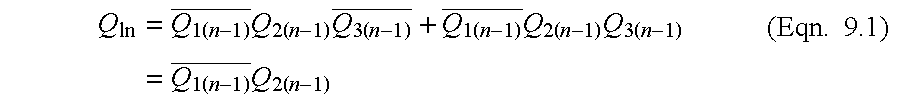
Q 1n ={overscore (Q1(n−1))} Q 2(n−1) {overscore (Q3(n−1))}  (Eqn. 9)
However, if the clock can go to state (1 0 0) also, the logic equation can be simplified as: Q ln = Q 1 ( n - 1 ) _ Q 2 ( n - 1 ) Q 3 ( n - 1 ) _ + Q 1 ( n - 1 ) _ Q 2 ( n - 1 ) Q 3 ( n - 1 ) = Q 1 ( n - 1 ) _ Q 2 ( n - 1 ) (Eqn.  9.1)
Figure US06452427-20020917-M00005
Using the same method, the logic equations for phases 2 and 3 can be obtained as
Q 2n ={overscore (Q1(n−1))} {overscore (Q2(n−1))}  (Eqn. 9.2)
Q 3n =Q 1(n−1) {overscore (Q2(n−1))}  (Eqn. 9.3)
The “don't care” phases are added in the true value table as shown in FIG. 8.
Two three-phase non-overlapping clock 116 can be constructed according to equations set forth above. An embodiment of a physical implementation (realization) for the clock is shown in FIG. 9. A high duty cycle clock is used as an input clock of the three-phase clock. Two edge-trigged D flip-flops are used to control the transition timing. Since the transition of D flip-flops occurs at the rising edge of the input clock, there will be no undesirable spike to cause erroneous turn-on of switches. The low period of input clock pulls all the outputs low, which produces the non-overlapping period between adjacent phases. Since the clock generator has “anti-lock” property, no reset is necessary to initiate the clock.
FIG. 10 illustrates a Schmitt oscillator (clock generator) for providing a high duty cycle pulse for the three-phase clock generator of FIG. 9. The low period will be used to produce the non-overlapping period. The high period is converted to the high period of each phase of the three-phase clock by the sequence desired. The charging and discharging of the capacitor Cosc is achieved by a non-symmetric inverter whose pMOS has a lower driving capacity than that of nMOS, so that Cosc can be charged slowly up to the high threshold voltage of the Schmitt trigger to provide a long positive period of the pulse. FIG. 11 illustrates the schematic timing diagram of the Schmitt trigger input clock generator of FIG. 10 and the three-phase non-overlapping clock generator of FIG. 9. The ratio of (W/L)p/(W/L)n is 3/10. which will give the nMOS about 10 times driving power than the pMOS considering μn≈3μp. Therefore, the duty cycle of the clock is 90.9%.
Conversion of Capacitance-to-current
The conversion of capacitance-to-current is realized by the charge difference on the measuring capacitor and the reference capacitor. The charging and discharging process are important in the conversion, especially the discharging process since it controls the total charge which can be converted to current. To simplify the discharging process analysis, the resistance of the analog switch is represented by a linear resistor, R. When the voltage VDS of a MOSFET is greater than the saturation voltage which is VGS−VT, the MOSFET works in the saturation region. The first-order expression of the drain current can be expressed as:
I=k′(V G −V T)2  (Eqn. 10) where k = μ C ox 2 W L
Figure US06452427-20020917-M00006
The gate voltage VG can be expressed using saturation current by V G = 1 k + V T (Eqn.  11)
Figure US06452427-20020917-M00007
By Kirchoff's law, we have V C = IR + V G = IR + I k + V T (Eqn.  12.1)
Figure US06452427-20020917-M00008
taking time derivative of both sides and substitute {square root over (I)} with Y, V C t = 2 RY Y t + 1 k Y t (Eqn.  12.2)
Figure US06452427-20020917-M00009
substitute V C t
Figure US06452427-20020917-M00010
using the equation I = - C V C t ,
Figure US06452427-20020917-M00011
- Y 2 C = 2 RY Y t + 1 k Y t (Eqn.  12.3) dt = - 2 RC dY Y - C k dY Y 2 (Eqn.  13)
Figure US06452427-20020917-M00012
integrating both sides from 0 to t. t = C k ( 1 Y - 1 Y 0 ) + 2 RC ln Y 0 Y = C k ( 1 I - 1 I 0 ) + 2 RC ln I 0 I = C k ( 1 V - V T - 1 V i - V T ) + 2 RC ln V i - V T V - V T (Eqn.14)
Figure US06452427-20020917-M00013
The time, t, is the time required for the gate voltage started at Vi to drop to V. It can be observed that R has to be made small and k′ be large in order to reduce the discharging time, t.
It is impractical to use low frequency in the capacitance-to-current converter to discharge the voltage on the capacitor to VT. Based on the fact that the rate at which the voltage on the capacitor drops is slow when the gate voltage is close to the threshold voltage [4.10], the proper operation frequency can be chosen to obtain a satisfied accuracy. Ideally, the total charge which is used in the conversion is (Vg−VT)Cx, assuming the voltage on the capacitor Cx has been discharged from Vg to VT during the discharging process. If the discharging time is not long enough, there is a residual voltage ΔV, which differs from VT existed on Cx. The charge is used in the conversion now is [Vg−(VT+ΔV]Cx=[Vg−ΔV−VT]Cx, where ΔV is the residual voltage. The residual voltage during the discharging process can be considered as a decreased charging voltage Vg. The output frequency error, because of the decreased Vg can be derived as following:
Take derivative of Eqn. 2 respect to Vg F V g = I V g 2 V c C st = fC x 2 V c C st (Eqn.  16.1) F = - fC x 2 V c C st V g (Eqn.  16.2) F F = C x V g ( V g - V T ) C x - ( V o - V T ) C 0 (Eqn.  16.3)
Figure US06452427-20020917-M00014
The allowed variation of the charging voltage Vg is dependent on the accuracy of the output required frequency. From equation Eqn. 16.3, we have: V g = F F ( V g - V T ) C x - ( V o - V T ) C o C x (Eqn.  17)
Figure US06452427-20020917-M00015
According to equation Eqn. 17, the maximum residual voltage ΔV on the capacitor before the voltage is discharged to VT can be determined. For an example, if the maximum error of output frequency is allowed to be 0.1% in the measurement range of 10 pF. Vg=Vo=4.5 v, Cƒ=1.0 pF. The residual voltage can be allowed to be 3.24 mv. Using equation Eqn. 14, the discharging time can be obtained when the V−VT is substituted by the residual voltage. Therefore, the operation frequency can be determined by the calculated discharging time. The clock frequency can be expressed in term of discharging time: f = 1 3 T dis + 2 T non - overlap (Eqn.  18)
Figure US06452427-20020917-M00016
Other techniques to reduce ΔV can be developed so that the clock frequency can be increased.
Resolution of the C-F Converter
The resolution of the C-F converter 110/112 is defined as the minimum capacitance that the converter can detect. If the same voltage are used for Vg and Vo, output frequency F in equation Eqn. 2 can be simplified as: F = ( V g - V T ) ( C x - C o ) f 2 V c C st (Eqn.  19.1)
Figure US06452427-20020917-M00017
When the measured capacitance Cx is increased by ΔC, the output frequency F ΔC can be obtained as: F Δ C = ( V g - V T ) ( C x + Δ C - C o ) f 2 V c C st (Eqn.  19.2)
Figure US06452427-20020917-M00018
The difference of output frequency is: Δ F = F Δ c - F = ( V g - V T ) f Δ C 2 V C C st (Eqn.  19.3)
Figure US06452427-20020917-M00019
The resolution of the converter can be expressed as: Δ C = Δ F f 2 V C C st V g - V T (Eqn.  20)
Figure US06452427-20020917-M00020
In the equation Eqn. 19, Vc is the threshold voltage of the Schmitt trigger and cannot be adjusted due to circuit configuration. However, the resolution of the converter, ΔC, can be designed by choosing the ratio of Cst/ƒVg under the condition that ΔF is greater than 1 Hz which is determined by the external measurement instrument. FIG. 12 shows that the resolution of the C-F converter (110/112) can be 0.01 pF when the parameters of the circuit listed are chosen.
Temperature Characteristics Analysis
Temperature characteristics of the C-F converter 110/112 are discussed in this section in order to understand the temperature drift of the circuit. The temperature sensitivity of all three sub-circuits, capacitance-to-current converter 110, current-to-frequency converter 112 and clock generator 116, contribute to the temperature error of the C-F converter 110/112.
(a) Temperature Dependency of MOSFET Threshold Voltage, VT
The threshold voltage of MOS transistors is sensitive to temperature. It will introduce temperature drift of the CMOS based circuits. The parameter ΦF plays a dominant role in the temperature dependency of the threshold voltage of MOS transistors. The temperature dependency ΦF is given by: Φ F T = 1 T [ Φ F ± ( 3 2 kT q ) E g0 2 q ] (Eqn.  20)
Figure US06452427-20020917-M00021
in which “−” is used for an nMOS and “+” for a pMOS.
The parameter ΦF always decreases in absolute value when the temperature increases. The term Ego is dominant. As a result, for an nMOS, ΦF is positive and its dΦF/dT is negative. Since the nMOS is usually in the enhancement mode, its threshold voltage decreases in absolute value. On the other hand, for a pMOS, ΦF is negative and dΦF/dT is positive. The threshold voltage thus decreases in absolute value as well.
The temperature dependency of VT can be given by V T T = 2 ± γ 2 Φ F Φ F T (Eqn.  21)
Figure US06452427-20020917-M00022
with “+” for a nMOS and “−” for a pMOS.
For a nMOS, the V T T
Figure US06452427-20020917-M00023
is negative and for a pMOS the V T T
Figure US06452427-20020917-M00024
is positive. But the absolute value of V T T
Figure US06452427-20020917-M00025
can be estimated as 2 mv/K.
(b) Temperature Dependency of Capacitance-to-current Converter
The temperature error of the C/I converter 110 comes from the threshold voltage of MOSFETs in current mirrors which are temperature dependent. From the equation Eqn. 1, the temperature error of the current converted can be expressed as: I T = ( - C x V T T + C o V T T ) f + [ ( V g - V T ) C x - ( V o - V T ) C o ] f T = - V T T ( C x - C o ) f + [ ( V g - V T ) C x - ( V o - V T ) C o ] f T (Eqn.  22)
Figure US06452427-20020917-M00026
The temperature error of the current is proportional to the temperature drift of the threshold voltage and clock frequency.
(c) Temperature Dependency of Schmitt Trigger Circuit
The current-to-frequency converter and the clock generator are realized by the Schmitt trigger circuits. The temperature characteristics of the two sub-circuits are determined by the temperature dependency of the Schmitt trigger.
Using equations Eqn. 4 and Eqn. 6 the threshold voltage can be defined as V c = V H - V L = V DD + k1 k3 V Tn 1 + k1 k3 - V DD - V Tp 1 + k4 k6 k4 k6 (Eqn.  23)
Figure US06452427-20020917-M00027
The temperature error of Schmitt trigger is: V c T = k1 k3 1 + k1 k3 V Tn T + k4 k6 1 + k4 k6 V Tp T (Eqn.  24)
Figure US06452427-20020917-M00028
The temperature error of the Schmnitt trigger is proportional to the error of the threshold voltages of both pMOS and nMOS. The temperature drift can be determined as −1.525 mv/K according to equation Eqn. 24, where k1/k3=6/21 and k4/k6=18/36. FIG. 13 shows a Pspice simulation result of the temperature characteristics of the threshold voltage of the Schmitt trigger circuit used in the converter.
(d) Temperature Error of the capacitance-to-frequency Converter
The temperature error of the capacitance-to-frequency converter 110/112 comes from three major sub-circuits, the capacitance-to-current converter 110, Schmitt trigger (FIG. 10) and clock generator 116. The output frequency is given by: F = I 2 V c C st (Eqn.  25) F T = 1 2 V c C st I T - I 2 V c 2 C st V c T = 1 2 V c C st { - V Tn T ( C x - C o ) f + [ ( V g - V Tn ) C x - ( V o - V Tn ) C o ] f T - 1 V c V c T } = - f 2 V c C st [ ( C x - C o ) V Tn T + ( V g - V Tn ) C x - ( V o - V Tn ) C o V c V c T ] + ( V g - V Tn ) C x - ( V o - V Tn ) C o 2 V c C st f T (Eqn.  26)
Figure US06452427-20020917-M00029
As discussed before, both the threshold voltage of a nMOS and the threshold voltage of a Schmitt trigger have negative temperature coefficients. It can be noticed from equation Eqn. 26 that the ∂VT/∂T and ∂Vc/∂T have opposite signs with ∂ƒ/∂T. Therefore, the temperature error of the C/F converter circuit can be compensated if the clock frequency has an appropriate negative temperature coefficient. A temperature compensation method based on the temperature controlled saturation current of pMOS transistors is discussed in the following section.
Temperature Error Compensation for C-F Converter
For a MOSFET in saturation, the first-order expression of the drain current can be expressed as: I sat = μ C ox 2 W L ( V GS - V T ) 2 (Eqn.  27)
Figure US06452427-20020917-M00030
The temperature coefficient of the saturation current is determined by the temperature coefficient of both mobility of carriers in the inversion layer and the threshold voltage, VT, of the MOSFET. The mobility of holes and electrons can be a strong function of temperature, depending on the doping level, given by μ=CμT−n μ where Cμ and nμ are constants. The temperature dependency of the mobility itself is then given by; 1 μ μ T = - n u T (Eqn.  28)
Figure US06452427-20020917-M00031
For low doping levels, the value of nμ is about 1.5. The channel of a MOSFET has an average doping level that is at least the doping level of bulk (i.e. strong inversion condition). Therefore, the bulk doping level can be used to estimate the value of nμ. The result usually is close to 1.5.
Take time derivative to equation Eqn.27, I sat T = C ox 2 W L ( V GS - V T ) 2 μ T - μ C ox 2 W L 2 ( V GS - V T ) V T T (Eqn.  29.1)
Figure US06452427-20020917-M00032
Dividing Isat on both sides, 1 I sat I sat T = 1 μ μ T - 2 V Gs - V T V T T (Eqn.  29.2)
Figure US06452427-20020917-M00033
Substituting equation Eqn. 28 into equation Eqn. 29.2, 1 I sat I sat T = - n μ T - 2 V GS - V T V T T (Eqn.  30)
Figure US06452427-20020917-M00034
The two terms have different signs and can be compensating each other. It can be shown, theoretically and experimentally, that unique (and distinct) gate voltage exists for a given MOSFET that the drain current has a zero temperature coefficient.
Letting 1 I sat I sat T = 0 ,
Figure US06452427-20020917-M00035
the zero-temperature-coefficient gate-source voltage (VGSZ) can be determined by: V GSZ = V T - 2 T n μ ( V T T ) (Eqn.  31)
Figure US06452427-20020917-M00036
For a pMOS made by MOSIS, the VT is −0.9 v, using nμ=1.5, the zero temperature coefficient VGS can be estimated as −1.7 v at 300 K. FIGS. 14A and 14B show the drain current of a pMOS simulated by Pspice. Using VGS=−5 v in (a), the drain current changes from 161.055 μA to 106.663 μA in the temperature range between 0 to 100° C. The maximum error is 33.77%. Using VGS=−1.8115 v in (b), the transistor keeps the drain current of 11.779 μA at 0° C. and 100° C. The minimum drain current is 11.657 μA at 45° C. The maximum error is 1.035% with respect to the drain current at 0 ° C.
Using the principle discussed above, the clock generator used in the converter can be modified to have a controllable temperature characteristic. The diagram of the modified clock generator is shown in FIG. 15. As discussed hereinabove, the clock is realized by a Schmitt trigger. The input voltage of the Schmitt trigger is the voltage on the capacitor. Cst, charged and discharged by two MOSFETs. By biasing M1 at VGSZ, the charging current can be temperature stable. Since the charging time is the dominant factor determining the clock period in the high duty cycle clock, only the transistor M1 is biased to have a zero temperature coefficient drain current to simplified the design. Transistor Sc is used as a switch (hence, the “S” nomenclature) to control the charging process. When the output of the Schmitt trigger is low, the transistor Sc is “on” to connect power supply with a resistor network which gives the M1 a biasing gate voltage at VGSZ. The capacitor Cst is charged via the transistor M1 to the high threshold voltage. When the output of the Schmitt trigger is high, transistors Sc and M1 are off. Then the Cst is discharged via M2 at the maximum saturation current to the lower threshold voltage. Actually, M1 needs to be biased at VGSZ′, where |VGSZ′| is greater than |VGSZ |, so that it has a negative temperature coefficient in order to compensate the temperature errors of the threshold voltage of the Schmitt trigger and capacitance-to-current converter (see Eqn. 26). FIG. 16 shows the Pspice simulation results of a clock frequency in the temperature range of −25° C. to 100 ° C., where the M1 is biased at 1.818 v. The relative error with respect to the frequency at 25° C. is less than ±0.5%. FIG. 17 shows the output frequency of the capacitance-to-frequency converter when M1 is biased at different voltages. It can be shown that the temperature coefficient of the converter can vary from positive to negative depending on how the bias voltage of M1 is designed. TABLE 2 shows the relative temperature error of the converter in the range of −25° C.-100° C., which is defined as following: ɛ = F ( T ) - F ( 25 ° C . ) F ( 25 ° C . ) × 100 % (Eqn.  32)
Figure US06452427-20020917-M00037
The simulated results were used to design the circuit of the capacitance-to-frequency/voltage converter.
TABLE 2
Relative Temperature Error of C-F Converter
VR (v) no compensation 3.203 3.005 2.809
Error % +/−14.16 +/−7.19 +/−0.67 +/−5.33
Capacitance-to-Voltage Converter
The current obtained from the capacitance-to-current (C-I) converter 110 can also be used to provide DC voltage signal output 104. A combination of the capacitance-to-current (C-I) converter 110 and current-to-voltage (I-V) converter 114 constitute a capacitance-to-voltage converter “110/114”.
A difference current-to-voltage (I-V) converter 114 is shown in FIG. 18A. By using this circuit, a voltage output 104 can be obtained in addition to the frequency output 106 from the capacitance-to-frequency (C-F) converter 110/112. The equivalent small signal circuit of the V-I circuit is shown in FIG. 18B, where gmi, and rki are the transconductance and loading resistance of the drain of the ith MOSFET, respectively. From the small signal circuit, we have,
V 1=(I 1g m1 V 1)r I1  (Eqn. 32-1) V1 = r l1 I1 1 + g m1 r l1 (Eqn.  32-2)
Figure US06452427-20020917-M00038
V2=(I2−g m2 V1)r I2  (Eqn. 33) V3 = g m3 V2r l3 = ( I2 - g m2 V1 ) r l2 g m3 r l3 = ( I2 - g m2 r l1 I1 1 + g m1 r l1 ) r l2 g m3 r l3 (Eqn.  33)
Figure US06452427-20020917-M00039
when gm1=gm2 and gm1rI1>>1, then we have V3 = r l2 g m3 r l3 ( I2 - I1 ) = R ( I2 - I1 ) (Eqn.  34)
Figure US06452427-20020917-M00040
where the equivalent resistance R=rI2gm3rI3.
From the capacitance-to-frequency (C-F) converter 110/112, the current difference. Ix−Io, has been obtained and can be used as one of the inputs of I-V circuit 114. I2 can be generated using a similar principle used in the C-F converter. Using a reference capacitor, Cƒ, and output voltage V3 of the I-V circuit 114 to construct current mirrors as shown in FIG. 19 (compare FIG. 4), the current I2 can be obtained as I f = f ( V3 - V T ) ( C f + C stray - C stray ) = f ( V3 - V T ) C f (Eqn.  35)
Figure US06452427-20020917-M00041
The reference capacitor Cƒ is also called a feedback capacitor since the current generated by Cƒ is related to the output voltage V3. In order to eliminate the effect of the stray capacitor connected to the Cƒ, one null capacitor is connected to one of the current mirrors which has the same routing as Cƒ. The V3 can be rewritten as: V3 = R ( I2 - I1 ) = R ( I x - I o - I f ) = R ( K1C x - K2C o - K3C f ) = R [ f ( V g - V T ) C x - f ( V o - V T ) C o - f ( V3 - V T ) C f ] (Eqn.  36-1) V3 = Rf [ ( V g - V T ) C x - ( V o - V T ) C o - V T C f ] 1 + RfC f (Eqn.  36-2)
Figure US06452427-20020917-M00042
if RƒCƒ>>1 then V out = V3 = ( V g - V T ) C x - ( V o - V T ) C o - V T C f C f (Eqn.  36-3)
Figure US06452427-20020917-M00043
The output of the C-V converter 110/114 is independent of the clock frequency and the value of the equivalent resistor. The sensitivity of the converter is defined as:
S Cx =∂V/∂C x=(V g −V T)/C ƒ.  (Eqn. 37)
Thus, the sensitivity of the converter can be adjusted either by voltage Vg or capacitor Cƒ.
FIG. 20 is a graph illustrating the frequency and voltage outputs of the dual output converter 100. Each of the C-F and C-V converters 110/112 and 110/114, respectively, are adjusted to have the best linear characteristics in the test range. The C/V converter is first adjusted by varying Vo to get the offset voltage greater than 1.5 v. The span of the voltage output can be adjusted by changing the sensitivity of the circuit, normally by shunting the feedback capacitor, Cƒ. The frequency output can be adjusted by varying capacitor Cst, as discussed hereinabove. As illustrated in FIG. 20, the sensitivity of the C/V converter is 0.63 v/pF with non-linearity ±0.38% and the sensitivity of the C/F converter is 729 Hz/pF with non-linearity of ±0.61%. The sensitivity of the C/V converter is lower than the designed value because of large stray capacitance of Cƒ.
A dual output capacitance interface circuit (100) based on switched capacitor circuits and charge subtraction technique provides both voltage output (104) and frequency output (106). The circuit is programmable independently with sensitivity and offset adjustment, and is insensitive to fixed stray capacitance. A sensitivity of 350 Hz/pF has been achieved in the 10 pF measurement range with non-linearity less that ±0.6%. A higher capacitance-to-frequency (C-F) sensitivity can be obtained for a smaller capacitance measurement range. A voltage sensitivity of 3-4 v/pF can be achieved. In the temperature range of 25° C.-95° C., the offset temperature drift of the C-V converter is less than 5%. The sensitivity drift is less than 3.5%. The offset temperature drift of the C-F converter is about −16% and the sensitivity drift is also −16% in the temperature range of 25° C.-95° C.
A temperature compensation method is based on the fact that a MOSFET has a bias voltage VGS which can give the saturation current with a zero-temperature-coefficient (ZTC). Using this principle, a temperature compensated clock generator is utilized. The temperature characteristics of the clock frequency, which is related to the output frequency of the C-F converter, can be used to compensate the overall temperature error of the converter. In the temperature range from 25° C. to 95° C., the temperature coefficient of sensitivity, after temperature compensation, is 37 ppm/° C., and the temperature coefficient of offset is 86 ppm/° C. The extra current source results in a clock frequency with a positive temperature coefficient. Since the C-F converter has negative temperature coefficient and the output frequency is proportional to the clock frequency, the temperature error can be compensated. Measured results shows that after the compensation, the temperature drift, when the input capacitor is fixed as 6.6 pF, is ±0.3% and the sensitivity drift is ±0.8%. An alternative temperature compensation method is to use an external MOS current source and a thermistor with a positive temperature coefficient.
Although the invention has been illustrated and described in detail in the drawings and foregoing description, the same is to be considered as illustrative and not restrictive in character, it being understood that only preferred embodiments have been shown and described, and that all changes and modifications that come within the spirit of the invention are desired to be protected. Undoubtedly, many other “variations” on the “themes” set forth hereinabove will occur to one having ordinary skill in the art to which the present invention most nearly pertains, and such variations are intended to be within the scope of the invention, as disclosed herein.

Claims (2)

What is claimed is:
1. Dual output capacitance interface circuit for providing at least one signal indicative of a capacitance value of a condition-sensitive capacitance; the dual output capacitance interface circuit comprising:
a capacitance-to-current converter for providing a current signal indicative of the capacitance value of the condition-sensitive capacitance;
a current-to-voltage converter that is used to convert the current signal from the capacitance-to-current converter to a DC voltage output signal; and
a current-to-frequency converter that is used to convert the current signal from the capacitance-to-current converter to a frequency output signal, wherein the current-to-frequency converter comprises a Schmitt trigger having an input connected to the output of an oscillator comprised of current mirrors that are switched by an output of the Schmitt trigger, to alternately charge and discharge a fixed capacitor using a mirrored current that is proportional to the current signal from the capacitance-to-current converter, thereby producing a Schmitt trigger output that provides a symmetric square wave output signal with a frequency determined by the condition-sensitive capacitance.
2. Dual output capacitance interface circuit for providing at least two output signals indicative of a capacitance value of a condition-sensitive capacitance; the dual output capacitance interface circuit comprising:
a capacitance-to-current converter for providing a current signal indicative of the capacitance value of the condition-sensitive capacitance;
a current-to-voltage converter that is used to convert the current signal from the capacitance-to-current converter to a DC voltage output signal; and
a current-to-frequency converter that is used to convert the current signal from the capacitance-to-current converter to a frequency output signal.
US09/743,525 1998-07-07 1999-07-07 Dual output capacitance interface circuit Expired - Fee Related US6452427B1 (en)

Priority Applications (1)

Application Number Priority Date Filing Date Title
US09/743,525 US6452427B1 (en) 1998-07-07 1999-07-07 Dual output capacitance interface circuit

Applications Claiming Priority (3)

Application Number Priority Date Filing Date Title
US9190998P 1998-07-07 1998-07-07
PCT/US1999/015270 WO2000002014A1 (en) 1998-07-07 1999-07-07 Dual output capacitance interface circuit
US09/743,525 US6452427B1 (en) 1998-07-07 1999-07-07 Dual output capacitance interface circuit

Publications (1)

Publication Number Publication Date
US6452427B1 true US6452427B1 (en) 2002-09-17

Family

ID=22230253

Family Applications (2)

Application Number Title Priority Date Filing Date
US09/743,525 Expired - Fee Related US6452427B1 (en) 1998-07-07 1999-07-07 Dual output capacitance interface circuit
US09/743,432 Expired - Fee Related US6465271B1 (en) 1998-07-07 1999-07-07 Method of fabricating silicon capacitive sensor

Family Applications After (1)

Application Number Title Priority Date Filing Date
US09/743,432 Expired - Fee Related US6465271B1 (en) 1998-07-07 1999-07-07 Method of fabricating silicon capacitive sensor

Country Status (5)

Country Link
US (2) US6452427B1 (en)
EP (3) EP1093571B1 (en)
AU (2) AU5215099A (en)
DE (2) DE69908129D1 (en)
WO (2) WO2000002014A1 (en)

Cited By (17)

* Cited by examiner, † Cited by third party
Publication number Priority date Publication date Assignee Title
US20050270153A1 (en) * 2004-06-08 2005-12-08 Samsung Electronic Co., Ltd. Radio frequency identification tag for transmitting temperature data and method therefor
US6995672B1 (en) * 1999-05-17 2006-02-07 The Goodyear Tire & Rubber Co. Relaxation oscillator for transponder
US20060249847A1 (en) * 2005-05-03 2006-11-09 Rosemount Aerospace Inc. Substrate with bonding metallization
US20070013014A1 (en) * 2005-05-03 2007-01-18 Shuwen Guo High temperature resistant solid state pressure sensor
US20070144247A1 (en) * 2005-12-23 2007-06-28 Seesink Peter H Multiple function stable sensor circuitry
US20070289389A1 (en) * 2006-06-16 2007-12-20 Honeywell International Inc. Pressure transducer with differential amplifier
US20090108382A1 (en) * 2005-05-03 2009-04-30 Odd Harald Steen Eriksen Transducer for use in harsh environments
US7628309B1 (en) 2005-05-03 2009-12-08 Rosemount Aerospace Inc. Transient liquid phase eutectic bonding
US8519722B1 (en) * 2008-10-22 2013-08-27 Cypress Semiconductor Corporation Method and apparatus for testing projected capacitance matrices and determining the location and types of faults
US8616065B2 (en) 2010-11-24 2013-12-31 Honeywell International Inc. Pressure sensor
US8656772B2 (en) 2010-03-22 2014-02-25 Honeywell International Inc. Flow sensor with pressure output signal
US8695417B2 (en) 2011-01-31 2014-04-15 Honeywell International Inc. Flow sensor with enhanced flow range capability
US9003897B2 (en) 2012-05-10 2015-04-14 Honeywell International Inc. Temperature compensated force sensor
US9052217B2 (en) 2012-11-09 2015-06-09 Honeywell International Inc. Variable scale sensor
US20170324409A1 (en) * 2016-05-04 2017-11-09 Stmicroelectronics (Rousset) Sas Generator of numbers of oscillations
US10103721B2 (en) 2016-05-04 2018-10-16 Stmicroelectronics (Rousset) Sas Multiplexer structure
US10243543B2 (en) 2016-05-04 2019-03-26 Stmicroelectronics (Rousset) Sas Pulse counting circuit

Families Citing this family (83)

* Cited by examiner, † Cited by third party
Publication number Priority date Publication date Assignee Title
US7260371B1 (en) 1998-04-14 2007-08-21 The Goodyear Tire & Rubber Company Programmable modulation index for transponder
US6922134B1 (en) 1998-04-14 2005-07-26 The Goodyear Tire Rubber Company Programmable trimmer for transponder
WO2000036387A1 (en) * 1998-12-15 2000-06-22 Fraunhofer-Gesellschaft zur Förderung der angewandten Forschung e.V. Method of producing a micro-electromechanical element
DE69908661T2 (en) 1999-05-17 2004-04-29 The Goodyear Tire & Rubber Co., Akron RF TRANSPONDER WITH A RELAXATION OSCILLATOR AND METHOD FOR GENERATING AN OSCILLATING MEASURING SIGNAL IN AN RF TRANSPONDER
WO2000069663A1 (en) 1999-05-17 2000-11-23 The Goodyear Tire & Rubber Company Power-on reset for transponder
US6369712B2 (en) 1999-05-17 2002-04-09 The Goodyear Tire & Rubber Company Response adjustable temperature sensor for transponder
US6980084B1 (en) 1999-05-17 2005-12-27 The Goodyear Tire & Rubber Company Power-on reset for transponder
US6658928B1 (en) 1999-12-14 2003-12-09 The Goodyear Tire & Rubber Company Method of monitoring pressure in a pneumatic tire
US6775632B1 (en) 1999-12-14 2004-08-10 The Goodyear Tire & Rubber Company Calibration of a transponders for a tire pressure monitoring system
US6860153B2 (en) * 2000-02-22 2005-03-01 Simon Fraser University Gas pressure sensor based on short-distance heat conduction and method for fabricating same
US6704185B2 (en) * 2000-02-23 2004-03-09 National Center For Scientific Research Capacitive pressure-responsive devices and their fabrication
ITTO20010086A1 (en) * 2001-01-30 2002-07-30 St Microelectronics Srl PROCEDURE FOR SEALING AND CONNECTING PARTS OF ELECTROMECHANICAL, FLUID, OPTICAL MICROSYSTEMS AND DEVICE SO OBTAINED.
JP4378617B2 (en) * 2001-07-17 2009-12-09 Smc株式会社 Micro electromechanical sensor
JP4890689B2 (en) * 2001-07-24 2012-03-07 オリンパス株式会社 Three-dimensional structure manufacturing method and oscillator manufacturing method
FR2829292B1 (en) * 2001-08-31 2004-09-10 Atmel Grenoble Sa METHOD FOR MANUFACTURING COLOR IMAGE SENSOR WITH PLOT ON PLOT WELDED SUPPORT SUBSTRATE
US6933537B2 (en) * 2001-09-28 2005-08-23 Osram Opto Semiconductors Gmbh Sealing for OLED devices
US7312785B2 (en) 2001-10-22 2007-12-25 Apple Inc. Method and apparatus for accelerated scrolling
US7345671B2 (en) 2001-10-22 2008-03-18 Apple Inc. Method and apparatus for use of rotational user inputs
FI114825B (en) * 2002-02-13 2004-12-31 Vti Technologies Oy Method for reducing the temperature dependence of a capacitive sensor and the design of a capacitive sensor
US7333092B2 (en) 2002-02-25 2008-02-19 Apple Computer, Inc. Touch pad for handheld device
US6958255B2 (en) 2002-08-08 2005-10-25 The Board Of Trustees Of The Leland Stanford Junior University Micromachined ultrasonic transducers and method of fabrication
US6828802B2 (en) * 2002-08-16 2004-12-07 Rosemount Inc. Pressure measurement device including a capacitive sensor in an amplifier feedback path
EP1682859A4 (en) * 2003-08-11 2007-08-22 Analog Devices Inc Capacitive sensor
US20070152977A1 (en) 2005-12-30 2007-07-05 Apple Computer, Inc. Illuminated touchpad
US7499040B2 (en) 2003-08-18 2009-03-03 Apple Inc. Movable touch pad with added functionality
GB2406381B (en) * 2003-09-27 2005-10-12 Future Technology Sensors
US7495659B2 (en) 2003-11-25 2009-02-24 Apple Inc. Touch pad for handheld device
US8059099B2 (en) 2006-06-02 2011-11-15 Apple Inc. Techniques for interactive input to portable electronic devices
JP4052263B2 (en) * 2004-03-04 2008-02-27 株式会社デンソー Pressure sensor
US7347099B2 (en) * 2004-07-16 2008-03-25 Rosemount Inc. Pressure transducer with external heater
CN100555200C (en) 2004-08-16 2009-10-28 苹果公司 The method of the spatial resolution of touch sensitive devices and raising touch sensitive devices
US7560788B2 (en) * 2004-09-20 2009-07-14 General Electric Company Microelectromechanical system pressure sensor and method for making and using
US7121145B2 (en) * 2004-10-18 2006-10-17 Silverbrook Research Pty Ltd Capacitative pressure sensor
US7037746B1 (en) * 2004-12-27 2006-05-02 General Electric Company Capacitive micromachined ultrasound transducer fabricated with epitaxial silicon membrane
US20060276008A1 (en) * 2005-06-02 2006-12-07 Vesa-Pekka Lempinen Thinning
US7622782B2 (en) 2005-08-24 2009-11-24 General Electric Company Pressure sensors and methods of making the same
JP4535046B2 (en) * 2006-08-22 2010-09-01 ヤマハ株式会社 Capacitance sensor and manufacturing method thereof
US7679033B2 (en) * 2005-09-29 2010-03-16 Rosemount Inc. Process field device temperature control
US7880729B2 (en) 2005-10-11 2011-02-01 Apple Inc. Center button isolation ring
US20070152983A1 (en) 2005-12-30 2007-07-05 Apple Computer, Inc. Touch pad with symbols based on mode
EP1860418A1 (en) * 2006-05-23 2007-11-28 Sensirion AG A method for fabricating a pressure sensor using SOI wafers
EP2275793A1 (en) * 2006-05-23 2011-01-19 Sensirion Holding AG A pressure sensor having a chamber and a method for fabricating the same
US8743060B2 (en) 2006-07-06 2014-06-03 Apple Inc. Mutual capacitance touch sensing device
US8022935B2 (en) 2006-07-06 2011-09-20 Apple Inc. Capacitance sensing electrode with integrated I/O mechanism
US9360967B2 (en) 2006-07-06 2016-06-07 Apple Inc. Mutual capacitance touch sensing device
US7448277B2 (en) * 2006-08-31 2008-11-11 Evigia Systems, Inc. Capacitive pressure sensor and method therefor
US7795553B2 (en) 2006-09-11 2010-09-14 Apple Inc. Hybrid button
US8274479B2 (en) 2006-10-11 2012-09-25 Apple Inc. Gimballed scroll wheel
US8482530B2 (en) 2006-11-13 2013-07-09 Apple Inc. Method of capacitively sensing finger position
TWI317812B (en) * 2006-12-22 2009-12-01 Delta Electronics Inc Capacitance acceleration sensing structure
US20090015269A1 (en) * 2007-07-13 2009-01-15 Pinto Gino A Stray Capacitance Compensation for a Capacitive Sensor
US7910843B2 (en) 2007-09-04 2011-03-22 Apple Inc. Compact input device
US8683378B2 (en) 2007-09-04 2014-03-25 Apple Inc. Scrolling techniques for user interfaces
US8416198B2 (en) 2007-12-03 2013-04-09 Apple Inc. Multi-dimensional scroll wheel
US8125461B2 (en) 2008-01-11 2012-02-28 Apple Inc. Dynamic input graphic display
US8820133B2 (en) 2008-02-01 2014-09-02 Apple Inc. Co-extruded materials and methods
US9454256B2 (en) 2008-03-14 2016-09-27 Apple Inc. Sensor configurations of an input device that are switchable based on mode
JP5374077B2 (en) 2008-06-16 2013-12-25 ローム株式会社 MEMS sensor
EP2159558A1 (en) * 2008-08-28 2010-03-03 Sensirion AG A method for manufacturing an integrated pressure sensor
US7782133B2 (en) * 2008-09-03 2010-08-24 Infineon Technologies Ag Power amplifier with output power control
US8816967B2 (en) 2008-09-25 2014-08-26 Apple Inc. Capacitive sensor having electrodes arranged on the substrate and the flex circuit
JP2010098518A (en) * 2008-10-16 2010-04-30 Rohm Co Ltd Method of manufacturing mems sensor, and mems sensor
US8395590B2 (en) 2008-12-17 2013-03-12 Apple Inc. Integrated contact switch and touch sensor elements
US8024978B2 (en) * 2009-01-21 2011-09-27 Honeywell International Inc. Media isolated pressure transducer having boss comprising single metal diaphragm
JP5458981B2 (en) 2009-03-24 2014-04-02 カシオ計算機株式会社 Multiband antenna and electronic equipment
US9354751B2 (en) 2009-05-15 2016-05-31 Apple Inc. Input device with optimized capacitive sensing
US8209857B2 (en) * 2009-06-19 2012-07-03 The Regents Of The University Of Michigan Method of making a thin film device
US8872771B2 (en) 2009-07-07 2014-10-28 Apple Inc. Touch sensing device having conductive nodes
US8490495B2 (en) * 2010-05-05 2013-07-23 Consensic, Inc. Capacitive pressure sensor with vertical electrical feedthroughs and method to make the same
US8316717B2 (en) * 2010-06-29 2012-11-27 Rogue Valley Microdevices, Inc. Wireless self-powered monolithic integrated capacitive sensor and method of manufacture
JP5896665B2 (en) * 2011-09-20 2016-03-30 キヤノン株式会社 Method for manufacturing electromechanical transducer
EP2871456B1 (en) 2013-11-06 2018-10-10 Invensense, Inc. Pressure sensor and method for manufacturing a pressure sensor
EP2871455B1 (en) 2013-11-06 2020-03-04 Invensense, Inc. Pressure sensor
DE102014108748A1 (en) * 2014-06-23 2015-12-24 Endress + Hauser Gmbh + Co. Kg Capacitive differential pressure sensor and method for its manufacture
US9567204B2 (en) * 2014-08-29 2017-02-14 Taiwan Semiconductor Manufacturing Co., Ltd. Microelectrochemical systems (MEMS) device having a seal layer arranged over or lining a hole in fluid communication with a cavity of the MEMS device
US10131540B2 (en) 2015-03-12 2018-11-20 Taiwan Semiconductor Manufacturing Co., Ltd. Structure and method to mitigate soldering offset for wafer-level chip scale package (WLCSP) applications
EP3076146B1 (en) 2015-04-02 2020-05-06 Invensense, Inc. Pressure sensor
US20170256432A1 (en) * 2016-03-03 2017-09-07 Nexperia B.V. Overmolded chip scale package
US10083883B2 (en) * 2016-06-20 2018-09-25 Applied Materials, Inc. Wafer processing equipment having capacitive micro sensors
US11225409B2 (en) 2018-09-17 2022-01-18 Invensense, Inc. Sensor with integrated heater
CN220502678U (en) 2019-01-16 2024-02-20 株式会社村田制作所 Silicon substrate having cavity and cavity SOI substrate using the same
WO2020236661A1 (en) 2019-05-17 2020-11-26 Invensense, Inc. A pressure sensor with improve hermeticity
CN110510572B (en) * 2019-08-30 2022-06-10 西安电子科技大学 Capacitive pressure sensor and manufacturing method thereof

Citations (17)

* Cited by examiner, † Cited by third party
Publication number Priority date Publication date Assignee Title
US3288656A (en) 1961-07-26 1966-11-29 Nippon Electric Co Semiconductor device
US3993939A (en) 1975-01-07 1976-11-23 The Bendix Corporation Pressure variable capacitor
US4104595A (en) 1976-12-27 1978-08-01 Borg-Warner Corporation Signal translating circuit for variable area capacitive pressure transducer
US4392382A (en) 1981-03-09 1983-07-12 Motorola Inc. Linearized electronic capacitive pressure transducer
US4446447A (en) 1980-12-22 1984-05-01 Ford Motor Company Circuit for converting pressure variation to frequency variation
US4517622A (en) * 1983-08-29 1985-05-14 United Technologies Corporation Capacitive pressure transducer signal conditioning circuit
US4720623A (en) * 1986-05-01 1988-01-19 E. I. Du Pont De Nemours And Company Power control device for a resistance heater in an oven
EP0302654A2 (en) 1987-08-06 1989-02-08 United Technologies Corporation Method of sealing an electrical feedthrough in a semiconductor device
US4820971A (en) 1986-05-29 1989-04-11 Ko Wen Hsiung Precision impedance variation measurement circuit
DE9102748U1 (en) 1991-01-14 1991-07-04 Ploechinger, Heinz, Dipl.-Ing., 8130 Starnberg, De
EP0499841A1 (en) 1991-02-18 1992-08-26 Mitsubishi Denki Kabushiki Kaisha Dielectric constant detection apparatus for fuel
EP0610806A1 (en) 1993-02-12 1994-08-17 CSEM, Centre Suisse d'Electronique et de Microtechnique S.A. Capacitive absolute pressure sensor and procedure for fabrication of a plurality of such sensors
US5349864A (en) * 1993-07-07 1994-09-27 Kavlico Corporation System for comparing a reference signal with a filtered signal to detect pressure discontinuity
US5528452A (en) 1994-11-22 1996-06-18 Case Western Reserve University Capacitive absolute pressure sensor
US5546070A (en) 1993-09-02 1996-08-13 Bayerische Motoren Werke Ag Device for monitoring the air pressure of a tire in motor vehicles with a sensor
US5656781A (en) 1993-07-07 1997-08-12 Vaisala Oy Capacitive pressure transducer structure with a sealed vacuum chamber formed by two bonded silicon wafers
US5706565A (en) 1996-09-03 1998-01-13 Delco Electronics Corporation Method for making an all-silicon capacitive pressure sensor

Family Cites Families (13)

* Cited by examiner, † Cited by third party
Publication number Priority date Publication date Assignee Title
US5295395A (en) * 1991-02-07 1994-03-22 Hocker G Benjamin Diaphragm-based-sensors
EP0734589B1 (en) * 1993-12-13 1998-03-25 Honeywell Inc. Integrated silicon vacuum micropackage for infrared devices
US5453628A (en) * 1994-10-12 1995-09-26 Kobe Steel Usa, Inc. Microelectronic diamond capacitive transducer
US5736430A (en) * 1995-06-07 1998-04-07 Ssi Technologies, Inc. Transducer having a silicon diaphragm and method for forming same
US5600072A (en) * 1995-06-23 1997-02-04 Motorola, Inc. Capacitive pressure sensor and method for making the same
US5596144A (en) * 1995-08-04 1997-01-21 Delco Electronics Corporation Piezoresistive force rebalance accelerometer
US5721162A (en) * 1995-11-03 1998-02-24 Delco Electronics Corporation All-silicon monolithic motion sensor with integrated conditioning circuit
US5798556A (en) * 1996-03-25 1998-08-25 Motorola, Inc. Sensor and method of fabrication
US5936164A (en) * 1997-08-27 1999-08-10 Delco Electronics Corporation All-silicon capacitive pressure sensor
US5932809A (en) * 1998-02-17 1999-08-03 Delco Electronics Corporation Sensor with silicon strain gage
US6109113A (en) * 1998-06-11 2000-08-29 Delco Electronics Corp. Silicon micromachined capacitive pressure sensor and method of manufacture
US6074891A (en) * 1998-06-16 2000-06-13 Delphi Technologies, Inc. Process for verifying a hermetic seal and semiconductor device therefor
US6150681A (en) * 1998-07-24 2000-11-21 Silicon Microstructures, Inc. Monolithic flow sensor and pressure sensor

Patent Citations (17)

* Cited by examiner, † Cited by third party
Publication number Priority date Publication date Assignee Title
US3288656A (en) 1961-07-26 1966-11-29 Nippon Electric Co Semiconductor device
US3993939A (en) 1975-01-07 1976-11-23 The Bendix Corporation Pressure variable capacitor
US4104595A (en) 1976-12-27 1978-08-01 Borg-Warner Corporation Signal translating circuit for variable area capacitive pressure transducer
US4446447A (en) 1980-12-22 1984-05-01 Ford Motor Company Circuit for converting pressure variation to frequency variation
US4392382A (en) 1981-03-09 1983-07-12 Motorola Inc. Linearized electronic capacitive pressure transducer
US4517622A (en) * 1983-08-29 1985-05-14 United Technologies Corporation Capacitive pressure transducer signal conditioning circuit
US4720623A (en) * 1986-05-01 1988-01-19 E. I. Du Pont De Nemours And Company Power control device for a resistance heater in an oven
US4820971A (en) 1986-05-29 1989-04-11 Ko Wen Hsiung Precision impedance variation measurement circuit
EP0302654A2 (en) 1987-08-06 1989-02-08 United Technologies Corporation Method of sealing an electrical feedthrough in a semiconductor device
DE9102748U1 (en) 1991-01-14 1991-07-04 Ploechinger, Heinz, Dipl.-Ing., 8130 Starnberg, De
EP0499841A1 (en) 1991-02-18 1992-08-26 Mitsubishi Denki Kabushiki Kaisha Dielectric constant detection apparatus for fuel
EP0610806A1 (en) 1993-02-12 1994-08-17 CSEM, Centre Suisse d'Electronique et de Microtechnique S.A. Capacitive absolute pressure sensor and procedure for fabrication of a plurality of such sensors
US5349864A (en) * 1993-07-07 1994-09-27 Kavlico Corporation System for comparing a reference signal with a filtered signal to detect pressure discontinuity
US5656781A (en) 1993-07-07 1997-08-12 Vaisala Oy Capacitive pressure transducer structure with a sealed vacuum chamber formed by two bonded silicon wafers
US5546070A (en) 1993-09-02 1996-08-13 Bayerische Motoren Werke Ag Device for monitoring the air pressure of a tire in motor vehicles with a sensor
US5528452A (en) 1994-11-22 1996-06-18 Case Western Reserve University Capacitive absolute pressure sensor
US5706565A (en) 1996-09-03 1998-01-13 Delco Electronics Corporation Method for making an all-silicon capacitive pressure sensor

Non-Patent Citations (14)

* Cited by examiner, † Cited by third party
Title
Barth, Philip W. Silicon Fusion Bonding for Fabrication of Sensors, Actuators and Microstructures Sensors and Actuators, A21-A23 (1990) pp. 919-926.
Bourouina et al. Variational Method for Tensile Stress Evaluation and Application to Heavily Boron-Doped Square-Shaped Silicon Diaphragms Sensors and Actuators, A49 (1995) pp. 21-27.
Ding et al. Touch Mode Silicon Capacitive Pressure Sensors 1990 ASME Winter Annual Meeting Nov. 25, 1990, pp. 111-117.
Gui et al. High Aspect Ratio Single Crystalline Silicon Microstructures Fabricated With Multi Layer Substrates Transducers '97-1997 International Conference on Solid-State Sensors and Actuators vo. 1, Jun. 16-19, 1997 pp. 633-636, XP002121907 Chicago.
Hanneborg et al. A Capacitive Pressure Sensor With Low TC0 and High Long-Term Stability Sensors and Actuators, A21-A23 (1990) pp. 151-154.
Jornod et al. High-Precision Capacitive Absolute Pressure Sensor Sensors and Actuators vol. 17 (1989) pp. 415-421.
Ko et al. Touch Mode Capacitive Pressure Sensors Sensors and Actuators, 2303 (1999).
Maseech et al. Plastic Deformation of Highly Doped Silicon Sensors and Actuators, A21-A23 (1990) pp. 861-865.
Maszara et al. Bonding of Silicon Wafers for Silicon-on-Insulator J. Appl. Phys. vol. 64 (10) Nov. 15, 1988, pp. 4943-4950.
Peters et al. Ultra-Stable High-Temperature Pressure Sensors Using Silicon Fusion Bonding Sensors and Actuators, A21-A23 (1990) pp. 96-101.
Shimbo et al. Silicon-to-Silicon Direct Bonding Method, J. Appl. Phys. vol. 60 (8) Oct. 15, 1986 pp. 2987-2991.
Steinmann et al. Mechanical Behaviour of Micromachined Sensor Membranes Under Uniform External Pressure Affected By In-Plane Stresses Using a Ritz Method and Hermite Polynomials Sensors and Actuators, A48 (1995) pp. 37-46.
Wang et al. Modeling of Touch Mode Capacitive Sensors and Diaphragms Sensors and Actuators, 2302 (1999).
Wang et al. Si-To-Si Fusion Bonded Touch Mode Capacitive Pressure Sensors Mechatronics., vol. 8 Aug. 1998 pp 467-484, XP004134433 Pergamon Press, Oxford, U.K. ISSN: 0957-4158.

Cited By (30)

* Cited by examiner, † Cited by third party
Publication number Priority date Publication date Assignee Title
US6995672B1 (en) * 1999-05-17 2006-02-07 The Goodyear Tire & Rubber Co. Relaxation oscillator for transponder
US7268685B2 (en) * 2004-06-08 2007-09-11 Samsung Electronics Co., Ltd. Radio frequency identification tag for transmitting temperature data and method therefor
US20050270153A1 (en) * 2004-06-08 2005-12-08 Samsung Electronic Co., Ltd. Radio frequency identification tag for transmitting temperature data and method therefor
US20100047491A1 (en) * 2005-05-03 2010-02-25 Rosemount Aerospace Inc. Transient liquid phase eutectic bonding
US7952154B2 (en) 2005-05-03 2011-05-31 Rosemount Aerospace Inc. High temperature resistant solid state pressure sensor
US20070013014A1 (en) * 2005-05-03 2007-01-18 Shuwen Guo High temperature resistant solid state pressure sensor
US8460961B2 (en) 2005-05-03 2013-06-11 Rosemount Aerospace Inc. Method for forming a transducer
US7400042B2 (en) 2005-05-03 2008-07-15 Rosemount Aerospace Inc. Substrate with adhesive bonding metallization with diffusion barrier
US8013405B2 (en) 2005-05-03 2011-09-06 Rosemount Aerospsace Inc. Transducer with fluidly isolated connection
US20090108382A1 (en) * 2005-05-03 2009-04-30 Odd Harald Steen Eriksen Transducer for use in harsh environments
US7538401B2 (en) 2005-05-03 2009-05-26 Rosemount Aerospace Inc. Transducer for use in harsh environments
US20090203163A1 (en) * 2005-05-03 2009-08-13 Odd Harald Steen Eriksen Method for making a transducer
US7628309B1 (en) 2005-05-03 2009-12-08 Rosemount Aerospace Inc. Transient liquid phase eutectic bonding
US7642115B2 (en) 2005-05-03 2010-01-05 Rosemount Aerospace Inc. Method for making a transducer
US20060249847A1 (en) * 2005-05-03 2006-11-09 Rosemount Aerospace Inc. Substrate with bonding metallization
US20100065934A1 (en) * 2005-05-03 2010-03-18 Odd Harald Steen Eriksen Transducer
US20070144247A1 (en) * 2005-12-23 2007-06-28 Seesink Peter H Multiple function stable sensor circuitry
US7493823B2 (en) 2006-06-16 2009-02-24 Honeywell International Inc. Pressure transducer with differential amplifier
US20070289389A1 (en) * 2006-06-16 2007-12-20 Honeywell International Inc. Pressure transducer with differential amplifier
US8519722B1 (en) * 2008-10-22 2013-08-27 Cypress Semiconductor Corporation Method and apparatus for testing projected capacitance matrices and determining the location and types of faults
US8656772B2 (en) 2010-03-22 2014-02-25 Honeywell International Inc. Flow sensor with pressure output signal
US8616065B2 (en) 2010-11-24 2013-12-31 Honeywell International Inc. Pressure sensor
US8695417B2 (en) 2011-01-31 2014-04-15 Honeywell International Inc. Flow sensor with enhanced flow range capability
US9003897B2 (en) 2012-05-10 2015-04-14 Honeywell International Inc. Temperature compensated force sensor
US9052217B2 (en) 2012-11-09 2015-06-09 Honeywell International Inc. Variable scale sensor
US20170324409A1 (en) * 2016-05-04 2017-11-09 Stmicroelectronics (Rousset) Sas Generator of numbers of oscillations
US10075166B2 (en) * 2016-05-04 2018-09-11 Stmicroelectronics (Rousset) Sas Generator of numbers of oscillations
US10103721B2 (en) 2016-05-04 2018-10-16 Stmicroelectronics (Rousset) Sas Multiplexer structure
US10243543B2 (en) 2016-05-04 2019-03-26 Stmicroelectronics (Rousset) Sas Pulse counting circuit
US10659020B2 (en) 2016-05-04 2020-05-19 Stmicroelectronics (Rousset) Sas Pulse counting circuit

Also Published As

Publication number Publication date
EP1101079A1 (en) 2001-05-23
AU5215099A (en) 2000-01-24
EP1101079B1 (en) 2003-09-10
EP1093571A1 (en) 2001-04-25
US6465271B1 (en) 2002-10-15
WO2000002014A1 (en) 2000-01-13
AU4971799A (en) 2000-01-24
DE69911218D1 (en) 2003-10-16
EP1271121A3 (en) 2003-05-02
DE69908129D1 (en) 2003-06-26
EP1271121A2 (en) 2003-01-02
EP1093571B1 (en) 2003-05-21
WO2000002028A1 (en) 2000-01-13

Similar Documents

Publication Publication Date Title
US6452427B1 (en) Dual output capacitance interface circuit
US5377524A (en) Self-testing capacitive pressure transducer and method
US5550516A (en) Integrated resonant microbeam sensor and transistor oscillator
US6145384A (en) Capacitive transducer having guard electrode and buffer amlifying means
US4812888A (en) Suspended gate field effect semiconductor pressure transducer device
US5431057A (en) Integratable capacitative pressure sensor
Guo et al. A monolithically integrated surface micromachined touch mode capacitive pressure sensor
WO2000022397A1 (en) Capacitive pressure sensor
EP3799311A1 (en) Waterproof mems button device, input device comprising the mems button device and electronic apparatus
US20180039363A1 (en) Array substrate, touch display panel, and touch display device thereof
KR20010032103A (en) Micromechanical differential pressure sensor device
KR20010083030A (en) Semiconductor pressure sensor
US6683358B1 (en) Silicon integrated accelerometer
Kudoh et al. An integrated miniature capacitive pressure sensor
US10171916B2 (en) System and method for a high-ohmic resistor
GB2174839A (en) Pressure sensitive field effect transistor
JPH0241184B2 (en)
JPH0554710B2 (en)
JPH02194343A (en) Semiconductor stress sensor
EP3803307B1 (en) Sensor arrangement and method of operating a sensor arrangement
JPS6294988A (en) Field effect pressure sensor
Martha et al. CMOS-MEMS Nano Force Sensor with Sub-μm U-Channel Suspended Gate SOIFET
JPH09257620A (en) Device for measuring displacement
Amendola et al. Self-biased transconductance amplifier
JPS5813313Y2 (en) Pressure-electric conversion device

Legal Events

Date Code Title Description
AS Assignment

Owner name: JPMORGAN CHASE BANK, NEW YORK

Free format text: THE MASTER GUARANTEE AND COLLATERIAL AGREEMENT;ASSIGNOR:GOODYEAR TIRE & RUBBER COMPANY, THE;REEL/FRAME:013913/0456

Effective date: 20030331

FPAY Fee payment

Year of fee payment: 4

AS Assignment

Owner name: THE GOODYEAR TIRE & RUBBER COMPANY, OHIO

Free format text: RELEASE BY SECURED PARTY;ASSIGNOR:JPMORGAN CHASE BANK, N.A.;REEL/FRAME:017996/0441

Effective date: 20060718

AS Assignment

Owner name: CASE WESTERN RESERVE UNIVERSITY, OHIO

Free format text: ASSIGNMENT OF ASSIGNORS INTEREST;ASSIGNOR:THE GOODYEAR TIRE & RUBBER COMPANY;REEL/FRAME:018194/0304

Effective date: 20060815

REMI Maintenance fee reminder mailed
LAPS Lapse for failure to pay maintenance fees
STCH Information on status: patent discontinuation

Free format text: PATENT EXPIRED DUE TO NONPAYMENT OF MAINTENANCE FEES UNDER 37 CFR 1.362

FP Lapsed due to failure to pay maintenance fee

Effective date: 20100917