US6464794B1 - Process chamber used in manufacture of semiconductor device, capable of reducing contamination by particulates - Google Patents
Process chamber used in manufacture of semiconductor device, capable of reducing contamination by particulates Download PDFInfo
- Publication number
- US6464794B1 US6464794B1 US09/404,631 US40463199A US6464794B1 US 6464794 B1 US6464794 B1 US 6464794B1 US 40463199 A US40463199 A US 40463199A US 6464794 B1 US6464794 B1 US 6464794B1
- Authority
- US
- United States
- Prior art keywords
- semiconductor wafer
- process chamber
- electrostatic chuck
- edge ring
- ring
- Prior art date
- Legal status (The legal status is an assumption and is not a legal conclusion. Google has not performed a legal analysis and makes no representation as to the accuracy of the status listed.)
- Expired - Fee Related
Links
Images


Classifications
-
- H—ELECTRICITY
- H01—ELECTRIC ELEMENTS
- H01L—SEMICONDUCTOR DEVICES NOT COVERED BY CLASS H10
- H01L21/00—Processes or apparatus adapted for the manufacture or treatment of semiconductor or solid state devices or of parts thereof
- H01L21/02—Manufacture or treatment of semiconductor devices or of parts thereof
- H01L21/04—Manufacture or treatment of semiconductor devices or of parts thereof the devices having at least one potential-jump barrier or surface barrier, e.g. PN junction, depletion layer or carrier concentration layer
- H01L21/18—Manufacture or treatment of semiconductor devices or of parts thereof the devices having at least one potential-jump barrier or surface barrier, e.g. PN junction, depletion layer or carrier concentration layer the devices having semiconductor bodies comprising elements of Group IV of the Periodic System or AIIIBV compounds with or without impurities, e.g. doping materials
- H01L21/30—Treatment of semiconductor bodies using processes or apparatus not provided for in groups H01L21/20 - H01L21/26
- H01L21/302—Treatment of semiconductor bodies using processes or apparatus not provided for in groups H01L21/20 - H01L21/26 to change their surface-physical characteristics or shape, e.g. etching, polishing, cutting
- H01L21/306—Chemical or electrical treatment, e.g. electrolytic etching
-
- H—ELECTRICITY
- H01—ELECTRIC ELEMENTS
- H01J—ELECTRIC DISCHARGE TUBES OR DISCHARGE LAMPS
- H01J37/00—Discharge tubes with provision for introducing objects or material to be exposed to the discharge, e.g. for the purpose of examination or processing thereof
- H01J37/32—Gas-filled discharge tubes
- H01J37/32431—Constructional details of the reactor
-
- C—CHEMISTRY; METALLURGY
- C23—COATING METALLIC MATERIAL; COATING MATERIAL WITH METALLIC MATERIAL; CHEMICAL SURFACE TREATMENT; DIFFUSION TREATMENT OF METALLIC MATERIAL; COATING BY VACUUM EVAPORATION, BY SPUTTERING, BY ION IMPLANTATION OR BY CHEMICAL VAPOUR DEPOSITION, IN GENERAL; INHIBITING CORROSION OF METALLIC MATERIAL OR INCRUSTATION IN GENERAL
- C23C—COATING METALLIC MATERIAL; COATING MATERIAL WITH METALLIC MATERIAL; SURFACE TREATMENT OF METALLIC MATERIAL BY DIFFUSION INTO THE SURFACE, BY CHEMICAL CONVERSION OR SUBSTITUTION; COATING BY VACUUM EVAPORATION, BY SPUTTERING, BY ION IMPLANTATION OR BY CHEMICAL VAPOUR DEPOSITION, IN GENERAL
- C23C16/00—Chemical coating by decomposition of gaseous compounds, without leaving reaction products of surface material in the coating, i.e. chemical vapour deposition [CVD] processes
- C23C16/44—Chemical coating by decomposition of gaseous compounds, without leaving reaction products of surface material in the coating, i.e. chemical vapour deposition [CVD] processes characterised by the method of coating
- C23C16/458—Chemical coating by decomposition of gaseous compounds, without leaving reaction products of surface material in the coating, i.e. chemical vapour deposition [CVD] processes characterised by the method of coating characterised by the method used for supporting substrates in the reaction chamber
- C23C16/4582—Rigid and flat substrates, e.g. plates or discs
- C23C16/4583—Rigid and flat substrates, e.g. plates or discs the substrate being supported substantially horizontally
- C23C16/4585—Devices at or outside the perimeter of the substrate support, e.g. clamping rings, shrouds
-
- C—CHEMISTRY; METALLURGY
- C23—COATING METALLIC MATERIAL; COATING MATERIAL WITH METALLIC MATERIAL; CHEMICAL SURFACE TREATMENT; DIFFUSION TREATMENT OF METALLIC MATERIAL; COATING BY VACUUM EVAPORATION, BY SPUTTERING, BY ION IMPLANTATION OR BY CHEMICAL VAPOUR DEPOSITION, IN GENERAL; INHIBITING CORROSION OF METALLIC MATERIAL OR INCRUSTATION IN GENERAL
- C23C—COATING METALLIC MATERIAL; COATING MATERIAL WITH METALLIC MATERIAL; SURFACE TREATMENT OF METALLIC MATERIAL BY DIFFUSION INTO THE SURFACE, BY CHEMICAL CONVERSION OR SUBSTITUTION; COATING BY VACUUM EVAPORATION, BY SPUTTERING, BY ION IMPLANTATION OR BY CHEMICAL VAPOUR DEPOSITION, IN GENERAL
- C23C16/00—Chemical coating by decomposition of gaseous compounds, without leaving reaction products of surface material in the coating, i.e. chemical vapour deposition [CVD] processes
- C23C16/44—Chemical coating by decomposition of gaseous compounds, without leaving reaction products of surface material in the coating, i.e. chemical vapour deposition [CVD] processes characterised by the method of coating
- C23C16/54—Apparatus specially adapted for continuous coating
-
- H—ELECTRICITY
- H01—ELECTRIC ELEMENTS
- H01J—ELECTRIC DISCHARGE TUBES OR DISCHARGE LAMPS
- H01J37/00—Discharge tubes with provision for introducing objects or material to be exposed to the discharge, e.g. for the purpose of examination or processing thereof
- H01J37/32—Gas-filled discharge tubes
- H01J37/32431—Constructional details of the reactor
- H01J37/32623—Mechanical discharge control means
- H01J37/32642—Focus rings
-
- H—ELECTRICITY
- H01—ELECTRIC ELEMENTS
- H01L—SEMICONDUCTOR DEVICES NOT COVERED BY CLASS H10
- H01L21/00—Processes or apparatus adapted for the manufacture or treatment of semiconductor or solid state devices or of parts thereof
- H01L21/67—Apparatus specially adapted for handling semiconductor or electric solid state devices during manufacture or treatment thereof; Apparatus specially adapted for handling wafers during manufacture or treatment of semiconductor or electric solid state devices or components ; Apparatus not specifically provided for elsewhere
- H01L21/683—Apparatus specially adapted for handling semiconductor or electric solid state devices during manufacture or treatment thereof; Apparatus specially adapted for handling wafers during manufacture or treatment of semiconductor or electric solid state devices or components ; Apparatus not specifically provided for elsewhere for supporting or gripping
- H01L21/6831—Apparatus specially adapted for handling semiconductor or electric solid state devices during manufacture or treatment thereof; Apparatus specially adapted for handling wafers during manufacture or treatment of semiconductor or electric solid state devices or components ; Apparatus not specifically provided for elsewhere for supporting or gripping using electrostatic chucks
-
- H—ELECTRICITY
- H01—ELECTRIC ELEMENTS
- H01L—SEMICONDUCTOR DEVICES NOT COVERED BY CLASS H10
- H01L21/00—Processes or apparatus adapted for the manufacture or treatment of semiconductor or solid state devices or of parts thereof
- H01L21/67—Apparatus specially adapted for handling semiconductor or electric solid state devices during manufacture or treatment thereof; Apparatus specially adapted for handling wafers during manufacture or treatment of semiconductor or electric solid state devices or components ; Apparatus not specifically provided for elsewhere
- H01L21/683—Apparatus specially adapted for handling semiconductor or electric solid state devices during manufacture or treatment thereof; Apparatus specially adapted for handling wafers during manufacture or treatment of semiconductor or electric solid state devices or components ; Apparatus not specifically provided for elsewhere for supporting or gripping
- H01L21/687—Apparatus specially adapted for handling semiconductor or electric solid state devices during manufacture or treatment thereof; Apparatus specially adapted for handling wafers during manufacture or treatment of semiconductor or electric solid state devices or components ; Apparatus not specifically provided for elsewhere for supporting or gripping using mechanical means, e.g. chucks, clamps or pinches
- H01L21/68714—Apparatus specially adapted for handling semiconductor or electric solid state devices during manufacture or treatment thereof; Apparatus specially adapted for handling wafers during manufacture or treatment of semiconductor or electric solid state devices or components ; Apparatus not specifically provided for elsewhere for supporting or gripping using mechanical means, e.g. chucks, clamps or pinches the wafers being placed on a susceptor, stage or support
- H01L21/68735—Apparatus specially adapted for handling semiconductor or electric solid state devices during manufacture or treatment thereof; Apparatus specially adapted for handling wafers during manufacture or treatment of semiconductor or electric solid state devices or components ; Apparatus not specifically provided for elsewhere for supporting or gripping using mechanical means, e.g. chucks, clamps or pinches the wafers being placed on a susceptor, stage or support characterised by edge profile or support profile
-
- H—ELECTRICITY
- H01—ELECTRIC ELEMENTS
- H01L—SEMICONDUCTOR DEVICES NOT COVERED BY CLASS H10
- H01L21/00—Processes or apparatus adapted for the manufacture or treatment of semiconductor or solid state devices or of parts thereof
- H01L21/02—Manufacture or treatment of semiconductor devices or of parts thereof
- H01L21/04—Manufacture or treatment of semiconductor devices or of parts thereof the devices having at least one potential-jump barrier or surface barrier, e.g. PN junction, depletion layer or carrier concentration layer
- H01L21/18—Manufacture or treatment of semiconductor devices or of parts thereof the devices having at least one potential-jump barrier or surface barrier, e.g. PN junction, depletion layer or carrier concentration layer the devices having semiconductor bodies comprising elements of Group IV of the Periodic System or AIIIBV compounds with or without impurities, e.g. doping materials
- H01L21/30—Treatment of semiconductor bodies using processes or apparatus not provided for in groups H01L21/20 - H01L21/26
- H01L21/31—Treatment of semiconductor bodies using processes or apparatus not provided for in groups H01L21/20 - H01L21/26 to form insulating layers thereon, e.g. for masking or by using photolithographic techniques; After treatment of these layers; Selection of materials for these layers
- H01L21/3205—Deposition of non-insulating-, e.g. conductive- or resistive-, layers on insulating layers; After-treatment of these layers
- H01L21/321—After treatment
- H01L21/3213—Physical or chemical etching of the layers, e.g. to produce a patterned layer from a pre-deposited extensive layer
- H01L21/32133—Physical or chemical etching of the layers, e.g. to produce a patterned layer from a pre-deposited extensive layer by chemical means only
- H01L21/32135—Physical or chemical etching of the layers, e.g. to produce a patterned layer from a pre-deposited extensive layer by chemical means only by vapour etching only
- H01L21/32136—Physical or chemical etching of the layers, e.g. to produce a patterned layer from a pre-deposited extensive layer by chemical means only by vapour etching only using plasmas
-
- Y—GENERAL TAGGING OF NEW TECHNOLOGICAL DEVELOPMENTS; GENERAL TAGGING OF CROSS-SECTIONAL TECHNOLOGIES SPANNING OVER SEVERAL SECTIONS OF THE IPC; TECHNICAL SUBJECTS COVERED BY FORMER USPC CROSS-REFERENCE ART COLLECTIONS [XRACs] AND DIGESTS
- Y10—TECHNICAL SUBJECTS COVERED BY FORMER USPC
- Y10T—TECHNICAL SUBJECTS COVERED BY FORMER US CLASSIFICATION
- Y10T117/00—Single-crystal, oriented-crystal, and epitaxy growth processes; non-coating apparatus therefor
- Y10T117/10—Apparatus
Definitions
- the present invention relates to equipment for manufacturing semiconductor devices, and more particularly, to a process chamber used in the manufacture of semiconductor devices, capable of reducing contamination by particulates.
- ICs integrated circuits
- semiconductor wafers formed of, for example, silicon.
- steps for example, photo masking, deposition of material layers, oxidation, nitridation, ion implantation, diffusion and etching, are conducted to obtain a final product.
- Most of these steps are carried out in a process chamber.
- Particulates are generated in a process chamber depending on the structure of the process chamber, the material used to form the chamber, and the types of reaction gases used in the chamber.
- the process chamber is contaminated by particulates due to the following two reasons.
- the first reason which usually occurs in a process chamber used for etching, is the difference in temperature between edge rings (or focus rings) near a semiconductor wafer and the parts from which the process chamber is constructed.
- the second reason which usually occurs in a process chamber used for a deposition process, is the unsmooth flow of a reaction gas near guide rings for guiding the edge of a semiconductor wafer.
- FIG. 1 is a view illustrating the generation of particulates in a process chamber during an etching process.
- FIG. 1 is a sectional view illustrating an electrostatic chuck supporting a semiconductor wafer in a conventional process chamber for an etching process using plasma.
- FIG. 2 is an enlarged view of the edge (portion A) of the semiconductor wafer shown in FIG. 1, and
- FIG. 3 is a plan view of FIG. 1 .
- an electrostatic chuck 20 holds a semiconductor wafer 10 using electrostatic adsorption.
- a power supply for supplying a high voltage is connected to the electrostatic chuck 20 to induce static electricity.
- Lift pins 21 for moving the semiconductor wafer 10 up and down when loading or unloading the semiconductor wafer 10 pass through the center of the electrostatic chuck 20 .
- the lift pins 21 are in contact with a support plate 22 installed below the electrostatic chuck 20 .
- the support plate 22 moves upwards in response to force applied by an external lifter (not shown), in a direction indicated by an arrow 23 .
- the lift pins 21 move upwards in response to upward movement of the support plate 22 .
- the lift pins 21 protrude past the surface of the electrostatic chuck 20 , and the semiconductor wafer 10 supported by the lift pins 21 is separated from the surface of the electrostatic chuck 20 .
- Edge rings 24 are installed at the upper edges of the electrostatic chuck 20 to fix the semiconductor wafer 10 . As shown in FIGS. 2 and 3, the edge ring 24 is separated from the edge of the semiconductor wafer 10 by a small gap 25 . Also, there is a space 26 between part of the surface of the edge ring 24 and the periphery of the bottom surface of the semiconductor wafer 10 . Also, a coupling ring 27 made of aluminum (Al) is interposed between the edge ring 24 and the electrostatic chuck 20 . The semiconductor wafer 10 is surrounded by a focus ring 28 . The focus ring 28 draws a plasma forming region to the edge of the semiconductor wafer 10 during the etching process, such that the plasma forming region is uniformly formed across the semiconductor wafer 10 .
- Al aluminum
- plasma enters into the small gap 25 between the edge ring 24 and the edge of the semiconductor wafer 10 , and thus the bottom surface of the semiconductor wafer may be etched.
- Polymers which are byproducts generated by the etching, adhere to the bottom surface of the semiconductor wafer 10 and bind the edge ring 24 to the electrostatic chuck 20 .
- the edge ring 24 can be broken due to it being bound to the electrostatic chuck 20 by the polymer.
- the edge ring 24 is etched along its inner circumference, so that the gap between the edge ring 24 and the semiconductor wafer 10 becomes wider. As a result, the edge ring 24 strikes against the edge of a platen zone of the semiconductor wafer (portion B of FIG. 3 ), so that a part of the semiconductor wafer 10 can be broken.
- FIG. 4 is another view illustrating the generation of particulates in a process chamber used for an etching process.
- FIG. 4 is a sectional view of an electrostatic chuck 20 in which a focus ring 40 is included but not the edge ring shown in FIG. 3 .
- a semiconductor wafer 10 is held by an electrostatic force produced by an electrostatic chuck 20 , through which lift pins 21 are inserted.
- An annular focus ring 40 is arranged around the edge of the electrostatic chuck 20 .
- the focus ring 40 draws a plasma forming region to the edge of the semiconductor wafer 10 during the etching process, such that the plasma forming region is uniformly formed across the semiconductor wafer 10 . Further, the focus ring 40 acts as an edge ring, thereby preventing the semiconductor wafer 10 from deviating from its original position.
- the upper part of the focus ring 40 is rounded, and the height of the focus ring is higher than the surface of the semiconductor wafer 10 .
- Most of the polymers generated in the process chamber accumulate on the protruding top of the focus ring 40 .
- the amount and type of accumulated polymer varies according to the material forming the metal layer to be etched, and the distribution in temperature in the reaction chamber. For example, if a metal layer to be etched is formed of tungsten (W), an etching gas used for etching the metal layer, for example, SF 6 , reacts with the Al component of the process chamber and increases the concentration of Al in the process chamber, thereby generating floating particulates of Al X F Y .
- an etching gas used for etching the metal layer for example, Cl 2 or BCl 3 , generates polymers of Al X Cl Y .
- Such polymers lie on the protruding portion of the focus ring 40 , which is the farthest away from a heat source (not shown), and may fall onto the semiconductor wafer 10 due to a change in internal pressure, thereby causing the process to fail.
- FIG. 5 is a sectional view illustrating the generation of particulates in a process chamber used for a deposition process.
- FIG. 5 shows a wafer support portion of a process chamber for chemical vapor deposition (CVD).
- FIG. 6 is an enlarged view of the portion C of FIG. 5 .
- a semiconductor wafer 10 is seated on a wafer chuck 50 , and a heater 51 is placed below the wafer chuck 50 .
- the semiconductor wafer 10 is guided by an annular guide ring 52 placed around the edge of the wafer chuck 50 .
- a space d between the guide ring 52 and the wafer chuck 50 is very narrow, a reaction gas is stagnant in the space d and does not flow smoothly therein. As a result, the reaction gases staying in the space d react with each other abnormally, which results in the growth of an undesirable material layer 53 .
- the material layer 53 may undesirably contaminate the wafer 10 .
- a process chamber used for etching or deposition produces particulates for various reasons, increasing the likelihood of failure of the semiconductor devices on wafer 10 .
- it would be desirable to prevent such a failure by eliminating factors which may cause the generation of particulates in the process chamber during the manufacturing of the devices.
- a process chamber for use in the manufacture of a semiconductor device changes the structure or material of the process chamber to suppress generation of particulates.
- a process chamber used in the manufacture of semiconductor device for etching a material on a semiconductor wafer using plasma includes an electrostatic chuck for holding the semiconductor wafer, and an annular edge ring which surrounds a side of the semiconductor wafer on the electrostatic chuck to prevent the semiconductor wafer from departing from its original position.
- the distance between the side of the semiconductor wafer and the first side is preferably less than 0.15 mm.
- a process chamber used in the manufacture of a semiconductor device for etching a material on a semiconductor wafer using plasma includes an electrostatic chuck for holding the semiconductor wafer, and an annular focus ring which surrounds the side of the semiconductor wafer on the electrostatic chuck to prevent the semiconductor wafer from departing from its original position and to make the plasma distribution uniform by drawing the plasma.
- the annular focus ring has a first side which faces the side of the semiconductor wafer and contacts the side of the semiconductor wafer.
- a process chamber used in the manufacture of a semiconductor device for etching a material on a semiconductor wafer using plasma includes an electrostatic chuck for holding the semiconductor wafer, a gas supply conduit, installed facing the upper surface of the semiconductor wafer, for supplying reaction gases to the upper space of the semiconductor wafer, wherein the gas supply conduit formed is slanted at a first angle with respect to the vertical direction, such that relatively more reaction gases are provided to a center of the semiconductor wafer than to a periphery of the semiconductor wafer, and a radio frequency power source for forming plasma in the upper space of the semiconductor wafer by ionizing the supplied reaction gases.
- a process chamber used in the manufacture of a semiconductor device for etching a material layer on a semiconductor wafer using plasma includes an electrostatic chuck for holding the semiconductor wafer, a slit valve, attached to a sidewall of the process chamber and separated by a first distance from the electrostatic chuck, having a wafer transfer path through which the semiconductor wafer placed above the electrostatic chuck can be loaded or unloaded in the horizontal direction from or to the outside of the process chamber, wherein the temperature of the slit valve is maintained at a higher temperature than the sidewall of the process chamber during an etching process.
- a process chamber used in the manufacture of a semiconductor device for depositing a material layer on a semiconductor wafer includes an electrostatic chuck for holding the semiconductor wafer, a heater installed below the wafer chuck, for supplying heat, and a guide ring for guiding the semiconductor wafer, the guide ring installed at the edge of an upper surface of the wafer chuck and separated from the chuck by about 15-25 mm.
- FIG. 1 is a sectional view of a wafer support portion in a conventional process chamber used in the manufacture of a semiconductor device
- FIG. 2 is an enlarged sectional view of the portion A shown in FIG. 1;
- FIG. 3 is a plan view of FIG. 1;
- FIG. 4 is a sectional view of another example of a wafer support portion in a conventional process chamber used in the manufacture of a semiconductor device;
- FIG. 5 is a sectional view of yet another example of a wafer support portion in a conventional process chamber used in the manufacture of a semiconductor device;
- FIG. 6 is an enlarged sectional view of the portion C of FIG. 5;
- FIG. 7 is a sectional view of a wafer support portion in a process chamber used in the manufacture of a semiconductor device in accordance with an aspect of the present invention.
- FIG. 8 is an enlarged sectional view of the portion D in FIG. 7;
- FIG. 9 is a plan view of FIG. 7;
- FIG. 10 is a sectional view of a wafer support portion in a process chamber used in the manufacture of a semiconductor device in accordance with an aspect of the present invention.
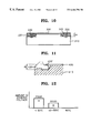
- FIG. 11 is a sectional view showing a focus ring used in a process chamber in accordance with an aspect of the present invention.
- FIG. 12 is a graph showing the adhering condition of polymer and the amount of adhering polymer with respect to the temperature across the surface of the focus ring shown in FIG. 11;
- FIG. 13 is a sectional view showing a sidewall of a process chamber in accordance with an aspect of the present invention.
- FIG. 14 is a sectional view showing a gas supply portion in a process chamber used in the manufacture of a semiconductor device in accordance with an aspect of the present invention.
- FIG. 15 is a sectional view showing a part of a process chamber used in the manufacture of a semiconductor device in accordance with an aspect of the present invention.
- FIG. 16 is a graph comparatively showing the amount of particulates generated in the processor chamber of FIG. 15 and in a conventional processor chamber;
- FIG. 17 is a sectional view of a wafer support portion in a process chamber used in the manufacture of a semiconductor device in accordance with an aspect of the present invention.
- FIG. 18 is an enlarged view of the portion E of FIG. 17;
- FIG. 19 is a plan view of FIG. 17;
- FIG. 20 is a plan view showing another example of the guide ring of FIG. 17.
- FIGS. 21A and 21B are graphs comparatively showing the amount of particulates generated in a conventional process chamber and the process chamber of FIG. 17 .
- the annular edge ring has a first side which faces the side of the semiconductor wafer and contacts the side of the semiconductor wafer.
- the edge ring preferably has a first upper surface which overlaps the periphery of the bottom surface of the semiconductor wafer and contacts the bottom surface of the semiconductor wafer.
- the edge ring may have a second side facing the side of the electrostatic chuck, the second side having a shape such that the contact area between the second side and the side of the electrostatic chuck is minimal.
- the second side of the edge ring may be slanted such that only the edge of the second side contacts the side of the electrostatic chuck.
- the edge ring may be fixed such that the edge ring cannot rotate. In this case, the edge ring may be fixed by a fixing pin, and may be fixed at two or more points separated from each other by a maximum distance.
- the edge ring is preferably made of quartz, silicon or aluminum nitride.
- the process chamber may further comprise a focus ring formed around the edge ring to make distribution of the plasma uniform.
- the focus ring preferably has a first upper surface which overlaps the periphery of the bottom surface of the semiconductor wafer and contacts the bottom surface of the semiconductor wafer.
- the focus ring may have a second side facing the side of the electrostatic chuck, and the second side preferably has a shape such that the contact area between the second side and the side of the electrostatic chuck is minimal.
- the second side of the focus ring may be slanted such that only the edge of the second side contacts the side of the electrostatic chuck.
- the focus ring is preferably fixed such that the edge ring cannot rotate.
- the edge ring may be fixed by a fixing pin.
- the focus ring may be fixed at two or more points separated from each other by a maximum distance.
- the focus ring is made of quartz, silicon or aluminum nitride.
- the surface temperature of the focus ring is maintained to be above at least 50° C. across the entire surface of the focus ring during a reaction.
- the upper surface of the focus ring is preferably flat without protrusions, and the upper surface, which is the farthest away from a heat source, is maintained to be above the surface temperature.
- the thickness of the focus ring, from the flat upper surface to the base thereof may be equal to or less than 20 mm.
- the slant angle of the gas supply path in the vertical direction is preferably at least 2 degrees, and the gas supply plate is preferably formed of quartz, silicon or aluminum nitride.
- Heat transfer lines are preferably formed to pass near the slit valve, and the number of the heat transfer lines formed near the slit valve is larger than the number of heat transfer lines formed passing through the sidewall. Also, the temperature of the upper part of the sidewall, which is positioned above the wafer transfer path, is the same as or higher than that of the lower part of the sidewall.
- the inner circumference of the guide ring comprises a first portion protruding toward the semiconductor wafer and separated from the semiconductor wafer by a first interval, and a second portion separated from the semiconductor wafer by a second interval which is longer than the first interval, to guide the semiconductor wafer.
- the first interval may be 0.5-1.0 mm
- the second interval may be 2-30 mm.
- the edge ring (or focus ring) and a semiconductor wafer preferably contact each other firmly, such that the plasma cannot enter below the bottom surface of the semiconductor wafer, thereby suppressing generation of particulates. Also, because the contact area between the edge ring (or focus ring) and the electrostatic chuck is minimized, the edge ring (or focus ring) can be easily separated from the electrostatic chuck even when particulates are generated. Also, the edge ring (or focus ring) is preferably fixed, so that bumping into the semiconductor wafer due to rotation of the edge ring can be prevented. Also, by changing the temperature distribution in the process chamber or the materials used for the process chamber, the generation of particulates, which depends on the temperature and materials of the process chamber, can be reduced such that the effect of the particulates on the semiconductor wafer can be minimized.
- the space between the guide ring and the wafer chuck can be maintained at a predetermined level such that reaction gases flow smoothly in the space, thereby suppressing the deposition of a foreign layer by reaction gases in the space between the guide ring and wafer chuck.
- FIG. 7 is a sectional view of an electrostatic chuck for supporting a semiconductor wafer in a process chamber used in the manufacture of a semiconductor device in accordance with an aspect of the present invention.
- FIG. 8 is an enlarged sectional view of the edge (portion D) of the semiconductor wafer of FIG. 7, and
- FIG. 9 is a plan view of FIG. 7 .
- an electrostatic chuck 200 holds a semiconductor wafer 100 by electrostatic adsorption.
- a power supply (not shown) for supplying a high voltage is connected to the electrostatic chuck 200 in order to induce static electricity.
- Lift pins 210 for moving the semiconductor wafer 100 up and down when loading or unloading the semiconductor wafer 100 pass through the center of the electrostatic chuck 200 .
- the lift pins 210 are in contact with a support plate 220 installed below the electrostatic chuck 200 .
- the support plate 220 can move upwards in response to a force applied by an external lifter (not shown), in a direction indicated by an arrow 230 .
- the lift pins 210 move upwards in response to upward movement of the support plate 220 . Then, the lift pins 210 protrude past the surface of the electrostatic chuck 200 and the semiconductor wafer 100 supported by the lift pins 210 is separated from the surface of the electrostatic chuck 200 .
- Edge rings 240 are installed at the upper edge of the electrostatic chuck 200 to fix the semiconductor wafer 100 .
- a coupling ring 270 made of, for example, aluminum (Al), is interposed between the edge ring 240 and the electrostatic chuck 200 .
- the semiconductor wafer 100 is surrounded by a focus ring 280 .
- the focus ring 280 draws a plasma forming region to the edge of the semiconductor wafer 100 during the etching process, such that the plasma forming region is uniformly formed across the semiconductor wafer 100 .
- FIG. 8 there is almost no gap between the edge ring 240 and the semiconductor wafer 100 .
- Such a gap between the edge ring 240 and the semiconductor wafer 100 can be reduced to about 0.1-0.15 mm. However, it is preferable to reduce the gap as much as possible.
- a space between the edge ring 240 and the periphery of the bottom surface of the semiconductor wafer 100 is reduced to a minimal distance. By minimizing the distance between the edge ring 240 and the semiconductor wafer 100 , infiltration of parasitic plasma into the space between the edge ring 240 and the bottom surface of the semiconductor wafer 100 can be suppressed as much as possible.
- the edge of the edge ring 240 which contacts the electrostatic chuck 200 , is preferably slanted, forming a triangular space at the contact region. As a result, only one edge point of the edge ring 240 contacts the electrostatic chuck 200 , so that the contact area between the edge ring and the electrostatic chuck 200 is minimized.
- the edge of the chuck may be slanted to create the triangular space. Thus, even when polymers accumulate at the periphery of the bottom surface of the semiconductor wafer 100 , a binding area between the edge ring 240 and the electrostatic chuck 200 by the polymers is minimized, so that the edge ring 240 can be easily separated from the semiconductor wafer 100 .
- the edge ring 240 is preferably fixed to the coupling ring 270 or the electrostatic chuck 200 (see FIGS. 7 and 8) by fixing pins 290 .
- the rotation of the edge ring 240 is prevented by the fixing pin 290 , so that damage to the semiconductor wafer, which may occur by the rotation of the edge ring 240 , can also be prevented.
- FIG. 10 is a sectional view of an electrostatic chuck for supporting a semiconductor wafer in a process chamber used in the manufacture of a semiconductor device in accordance with an aspect of the present invention.
- the process chamber of FIG. 10 is different from that of FIG. 7 in that only a focus ring is used without an edge ring.
- an electrostatic chuck 310 holds a semiconductor wafer 300 by electrostatic adsorption.
- a power supply (not shown) for supplying a high voltage is connected to the electrostatic chuck 310 in order to induce static electricity, and lift pins (not shown) which are moved when loading or unloading the semiconductor wafer 100 , pass through the electrostatic chuck 310 .
- an annular focus ring 320 is installed around the edge of the electrostatic chuck 310 .
- the focus ring 320 draws a plasma forming region to the edge of the semiconductor wafer 300 during the etching process, such that the plasma forming region is uniformly formed across the semiconductor wafer 300 .
- the focus ring 320 can also fix the semiconductor wafer 300 .
- the gap between the focus ring 320 and the semiconductor wafer 300 and the space between the focus ring 320 and the periphery of the bottom surface of the semiconductor wafer 300 are both minimized.
- the edge of the focus ring 320 facing the upper side of the electrostatic chuck 310 , is preferably slanted to reduce the contact area between the focus ring 320 and the electrostatic chuck 310 as much as possible.
- the edge of the chuck may be slanted to create the triangular space.
- the area between the focus ring 320 and the electrostatic chuck 310 , which is bound by polymers can be minimized, so that the focus ring 320 can be easily separated from the electrostatic chuck 310 without damage to the focus ring 320 .
- the focus ring 320 is fixed to the electrostatic chuck 310 by fixing pins 330 . Because the focus ring 320 is fixed, the focus ring 320 does not rotate even though the focus ring 320 is spaced further apart from the semiconductor wafer 300 . As a result, bumping of the focus ring 320 into the semiconductor wafer can be minimized or prevented.
- the upper surface of the focus ring 320 is partially etched during the etching process, so that the lifetime of the focus ring 320 is shortened.
- the thickness d 1 , of the focus ring 320 may affect the processing result, the thickness of the focus ring 320 must be restricted.
- the thickness d 1 of the focus ring 320 which is widely in use, is approximately 3.6 mm.
- the thickness d 1 of the focus ring was increased to approximately 4.5 mm.
- the lifetime of the focus ring 320 was increased by about 2-3 times, without affecting the processing result.
- FIG. 11 shows a focus ring in a process chamber used in the manufacture of a semiconductor device in accordance with an aspect of the present invention.
- a focus ring 420 used in a process chamber used in the manufacture of a semiconductor device is installed around the edge of the electrostatic chuck 410 and has an annular shape, such that the focus ring 420 is separated from the edge of the semiconductor wafer 400 by a predetermined distance.
- a portion 420 ′ of the focus ring 420 contacts firmly with the periphery of the bottom surface of the semiconductor wafer 400 in order to prevent parasitic plasma from infiltrating into the space between the bottom surface of the semiconductor wafer 400 and the focus ring 420 .
- the total height d 2 of the focus ring 420 is half that of the conventional focus ring.
- the total height d 2 of the focus ring used in a process chamber for manufacturing a semiconductor device can be less than 20 mm, preferably approximately 15 mm. That is, as shown in FIG. 11, the upper surface of the focus ring can be flattened by removing the protruding portion from a conventional focus ring (drawn with dashed lines), such that the temperature distribution across the surface of the focus ring 420 becomes uniform.
- the amount of polymer accumulated on the focus ring varies according to the difference in temperature of the focus ring.
- FIG. 12 is a graph showing the amount of adhered polymer with respect to the temperature at the surface of the focus ring.
- portion A at a portion of the focus ring at below 50° C.
- portion B Polymer also adheres to a portion of the focus ring at 50-55° C.
- portion B the amount of polymer adhering to the portion B is less than that adhering to the portion A, and the adhesion status is better than in the portion A.
- polymers do not adhere to a portion of the focus ring, at a temperature higher than 60° C.
- the amount of polymers adhering to the focus ring and the adhesion status of the polymers vary according to the difference in temperature at the surface of the focus ring.
- the reason for the occurrence of a temperature difference in the focus ring is that the distance from a heat source to each portion of the focus ring is different.
- a heater is installed below an electrostatic chuck as a heat source.
- the temperature of the focus ring is the highest at the base, and the temperature of the focus ring decreases toward the upper portion of the focus ring.
- the largest amount of polymers adheres to the upper protruding portion of the focus ring having the lowest temperature, and the adhesion status of the polymers at the upper portion is worst.
- a semiconductor wafer is placed adjacent to the protruding portion of the focus ring, and the semiconductor wafer can be deteriorated by the large amount of polymers which are poorly adhered to the focus ring.
- the temperature can be evenly distributed over the focus ring.
- the thickness of the focus ring is controlled such that the temperature of the focus ring is maintained at above 60° C., thereby reducing the amount of loosely adhered polymers.
- FIG. 13 is a sectional view showing a sidewall of a process chamber used for manufacturing a semiconductor device in accordance with an aspect of the present invention.
- a slit valve 520 for transferring a semiconductor wafer 560 is installed in a sidewall 510 attached to an external wall 500 of the process chamber.
- the sidewall 510 is formed of anodized aluminum (Al) and liners 530 a and 530 b are attached to the sidewall 510 , facing the inner space of the process chamber.
- the liners 530 a and 530 b are for preventing polymers from adhering to the sidewall 510 of the process chamber.
- the semiconductor wafer 560 is guided by a focus ring 550 placed on the wafer chuck 540 , and the liners 530 a and 530 b are separated from the semiconductor wafer 560 by a predetermined distance d 3 .
- a heater is placed below the wafer chuck 540 as a heat source.
- the temperatures of the liners 530 a and 530 b vary according to their height. For example, temperature of the lower liner 530 b, which is closer to the heater, is higher than that of the upper liner 530 b, which is farther from the heater.
- the temperature of the slit valve 520 which forms the wafer transfer path, can be increased as much as possible, thereby preventing the slit valve 520 from being contaminated by the polymers.
- more heat transfer lines passing near the slit valve 520 are installed than those passing through the sidewall 510 of the process chamber.
- FIG. 14 is a sectional view showing a gas supply portion used in a process chamber for manufacturing a semiconductor device in accordance with an aspect of the present invention.
- a gas supply plate 600 is located in a cover 610 of the process chamber.
- a gas supply line (not shown) for supplying gas is connected to the upper portion of the gas supply plate 600 .
- a reaction gas, such as an etching gas is supplied into the process chamber through holes 620 formed in the gas supply plate 600 .
- the energy of the etching gas supplied into the process chamber is increased by a high radio frequency (RF) power.
- RF radio frequency
- High energy gas molecules collide with neighboring neutral molecules, generating electrons and ions. Due to repeated collisions, a plasma 630 is formed in the reaction chamber, and in particular, above the semiconductor wafer 640 .
- the level of uniformity with which the plasma 630 is distributed greatly affects the result of the process. That is, the distribution of the plasma 630 must be uniform in the space on the semiconductor wafer 640 . However, the plasma 630 can be drawn to the edge of the semiconductor wafer 640 due to the focus ring formed around the semiconductor wafer 640 , so that the plasma 630 may be concentrated near the edge of the semiconductor wafer 640 . Thus, the structure of the holes 620 of the gas supply plate 600 , which directly affects the distribution of plasma 630 , is changed such that the density of the plasma 630 is higher at the center than near the edge of the semiconductor wafer 640 .
- the gas supply lines 620 which pass through the gas supply plate 600 are slanted such that gas discharge portions thereof point toward the center of the semiconductor wafer.
- the slant angle ⁇ of the gas discharge portion with respect to the vertical direction of the gas supply line 632 can be about 2-5°. If the angle a of the gas supply line 620 is too large, the plasma 630 is so dense at the center of the semiconductor substrate that the plasma 630 cannot distribute uniformly. Because the reaction gas is supplied toward the center of the semiconductor wafer 640 , the plasma density is locally increased at the center. However, since the focus ring draws the plasma, the distribution of plasma becomes uniform.
- the sidewall, gas supply plate, focus ring or edge ring of FIGS. 7-14 can be made of, for example, quartz, silicon or aluminum nitride. That is, when a metal layer to be etched is formed of tungsten (W), SF 3 is used as an etching gas for removing the tungsten layer, and Cl 2 and BCl 3 are used as etching gases for removing a barrier metal layer.
- SF 6 gas leads to isotropic etching by a reaction with Al 2 O 3 which is used to form a conventional focus ring, and increases etching damage by F ions, resulting in Al, F and O byproducts.
- the generation of byproducts can be suppressed by using quartz, silicon or aluminum nitride.
- FIG. 15 is a sectional view showing a part of a process chamber used in the manufacture of a semiconductor device in accordance with an aspect of the present invention.
- a semiconductor wafer 710 is seated on an electrostatic chuck 720 in a process chamber 700 .
- the electrostatic chuck 720 is placed on a support stand 730 .
- a semiconductor wafer 710 is guided by an annular focus ring 740 formed around the edge of the electrostatic chuck 720 .
- the focus ring 740 also makes the density of plasma uniform across the semiconductor wafer 710 .
- the focus ring 740 for these functions has an upper portion 750 .
- the thickness d 4 of the upper portion 750 of the focus ring 740 is controlled to be higher than the upper surface of the semiconductor wafer 710 .
- the thickness d 4 of the upper portion 750 is approximately 2.4-3.0 mm. If the thickness d 4 of the upper portion 750 is more than 3 mm, a wafer transfer means, for example, a robotic arm (not shown), used to transfer the semiconductor wafer 710 , may contact the upper portion 750 . If the thickness d 4 of the upper portion 750 is less than 2.4 mm, the original function of the upper portion 750 is deteriorated, thereby shortening the lifetime of the upper portion 750 .
- FIG. 16 is a graph comparatively showing the amount of particulates generated in a conventional process chamber and in a process chamber as shown in FIG. 15 .
- the conventional process chamber used for this comparison was a process chamber having a focus ring which has a wing extended in the vertical direction.
- FIG. 17 is a sectional view of another process chamber used in manufacturing a semiconductor device in accordance with an aspect of the present invention, and in particular, showing a wafer support portion in a process chamber for chemical vapor deposition (CVD).
- FIG. 18 is an enlarged view of the portion E of FIG. 17, and
- FIG. 19 is a plan view of FIG. 17 .
- a semiconductor wafer 800 is seated on a wafer chuck 810 , and a heater 820 is installed below the wafer chuck 810 .
- an annular guide ring 830 is arranged around the edge of the upper surface of the wafer chuck 810 .
- the guide ring 830 is for preventing the semiconductor wafer 800 from departing from its original position during the CVD process.
- the guide ring 830 is separated by a predetermined distance, for example, about 0.1-1.0 mm, from the semiconductor wafer 800 .
- the guide ring 830 is separated by a distance of approximately 15-25 mm from the upper surface of the wafer chuck 810 , which allows reaction gases to flow smoothly in the space. As a result, the formation of an undesirable layer can be suppressed.
- FIG. 20 is a plan view showing another example of the guide ring shown in FIG. 17 .
- a guide ring 830 ′ is separated by a first interval, for example, about 2-30 mm, from a semiconductor wafer 800 around its inner circumference, which permits the reaction gas to flow smoothly in the space between the semiconductor wafer 800 and the guide ring 830 ′.
- a plurality of protrusions 831 are spaced around the inner circumstance of the guide ring 830 ′, and the plurality of protrusions 831 are separated by a second interval which is smaller than the first interval, for example, about 0.5-1.0 mm, from the semiconductor wafer 800 .
- FIG. 21A is a graph showing the number of particulates generated in a conventional process chamber with respect to the number of processed wafers
- FIG. 21B is a graph showing the number of particulates in a process chamber as shown in FIG. 17 with respect to the number of processed wafers.
- ⁇ indicates the number of particulates having a diameter larger than 0.2 ⁇ m which are generated on the semiconductor wafer
- ⁇ indicates the number of particulates having a diameter larger than 0.2 ⁇ m which are generated in the process chamber.
- a cleaning process has to be performed using a predetermined cleaning gas, such as CIF 3 , after processing 500 sheets of semiconductor wafers. Nevertheless, when the number of processed semiconductor wafers reaches about 1000 sheets, a large amount of particulates are generated as shown in FIG. 21 A.
Abstract
Description
Claims (9)
Priority Applications (4)
| Application Number | Priority Date | Filing Date | Title |
|---|---|---|---|
| US10/234,135 US20030000648A1 (en) | 1998-09-23 | 2002-09-05 | Process chamber used in manufacture of semiconductor device, capable of reducing contamination by particulates |
| US10/235,976 US6797109B2 (en) | 1998-09-23 | 2002-09-06 | Process chamber used in manufacture of semiconductor device, capable of reducing contamination by particulates |
| US10/237,111 US20030013315A1 (en) | 1998-09-23 | 2002-09-09 | Process chamber used in manufacture of semiconductor device, capable of reducing contamination by particulates |
| US11/506,833 US20060278341A1 (en) | 1998-09-23 | 2006-08-21 | Process chamber used in manufacture of semiconductor device, capable of reducing contamination by particulates |
Applications Claiming Priority (4)
| Application Number | Priority Date | Filing Date | Title |
|---|---|---|---|
| KR19980039486 | 1998-09-23 | ||
| KR98-39486 | 1998-09-23 | ||
| KR99-22541 | 1999-06-16 | ||
| KR1019990022541A KR100292410B1 (en) | 1998-09-23 | 1999-06-16 | Process chamber for reducing particulate contamination for manufacturing semiconductor device |
Related Child Applications (3)
| Application Number | Title | Priority Date | Filing Date |
|---|---|---|---|
| US10/234,135 Division US20030000648A1 (en) | 1998-09-23 | 2002-09-05 | Process chamber used in manufacture of semiconductor device, capable of reducing contamination by particulates |
| US10/235,976 Division US6797109B2 (en) | 1998-09-23 | 2002-09-06 | Process chamber used in manufacture of semiconductor device, capable of reducing contamination by particulates |
| US10/237,111 Division US20030013315A1 (en) | 1998-09-23 | 2002-09-09 | Process chamber used in manufacture of semiconductor device, capable of reducing contamination by particulates |
Publications (1)
| Publication Number | Publication Date |
|---|---|
| US6464794B1 true US6464794B1 (en) | 2002-10-15 |
Family
ID=26634146
Family Applications (5)
| Application Number | Title | Priority Date | Filing Date |
|---|---|---|---|
| US09/404,631 Expired - Fee Related US6464794B1 (en) | 1998-09-23 | 1999-09-23 | Process chamber used in manufacture of semiconductor device, capable of reducing contamination by particulates |
| US10/234,135 Abandoned US20030000648A1 (en) | 1998-09-23 | 2002-09-05 | Process chamber used in manufacture of semiconductor device, capable of reducing contamination by particulates |
| US10/235,976 Expired - Fee Related US6797109B2 (en) | 1998-09-23 | 2002-09-06 | Process chamber used in manufacture of semiconductor device, capable of reducing contamination by particulates |
| US10/237,111 Abandoned US20030013315A1 (en) | 1998-09-23 | 2002-09-09 | Process chamber used in manufacture of semiconductor device, capable of reducing contamination by particulates |
| US11/506,833 Abandoned US20060278341A1 (en) | 1998-09-23 | 2006-08-21 | Process chamber used in manufacture of semiconductor device, capable of reducing contamination by particulates |
Family Applications After (4)
| Application Number | Title | Priority Date | Filing Date |
|---|---|---|---|
| US10/234,135 Abandoned US20030000648A1 (en) | 1998-09-23 | 2002-09-05 | Process chamber used in manufacture of semiconductor device, capable of reducing contamination by particulates |
| US10/235,976 Expired - Fee Related US6797109B2 (en) | 1998-09-23 | 2002-09-06 | Process chamber used in manufacture of semiconductor device, capable of reducing contamination by particulates |
| US10/237,111 Abandoned US20030013315A1 (en) | 1998-09-23 | 2002-09-09 | Process chamber used in manufacture of semiconductor device, capable of reducing contamination by particulates |
| US11/506,833 Abandoned US20060278341A1 (en) | 1998-09-23 | 2006-08-21 | Process chamber used in manufacture of semiconductor device, capable of reducing contamination by particulates |
Country Status (2)
| Country | Link |
|---|---|
| US (5) | US6464794B1 (en) |
| KR (1) | KR100292410B1 (en) |
Cited By (44)
| Publication number | Priority date | Publication date | Assignee | Title |
|---|---|---|---|---|
| US20020088546A1 (en) * | 2001-01-05 | 2002-07-11 | Seiko Epson Corporation | Dry etching apparatus |
| US6620736B2 (en) * | 2001-07-24 | 2003-09-16 | Tokyo Electron Limited | Electrostatic control of deposition of, and etching by, ionized materials in semiconductor processing |
| US20030192478A1 (en) * | 2002-04-16 | 2003-10-16 | Asm Japan K.K. | Plasma CVD apparatus comprising susceptor with ring |
| US20030224604A1 (en) * | 2002-05-31 | 2003-12-04 | Intel Corporation | Sacrificial polishing substrate for improved film thickness uniformity and planarity |
| US20040000375A1 (en) * | 2002-06-27 | 2004-01-01 | Taiwan Semiconductor Manufacturing Co., Ltd. | Plasma etch chamber equipped with multi-layer insert ring |
| US6676804B1 (en) * | 1998-07-16 | 2004-01-13 | Tokyo Electron At Limited | Method and apparatus for plasma processing |
| US20040040663A1 (en) * | 2002-08-29 | 2004-03-04 | Ryujiro Udo | Plasma processing apparatus |
| US20040083975A1 (en) * | 2002-09-20 | 2004-05-06 | Lam Research Corporation | Apparatus for reducing polymer deposition on a substrate and substrate support |
| US20040168642A1 (en) * | 1999-12-22 | 2004-09-02 | Kentaro Asakura | Film deposition system |
| US6828243B2 (en) * | 2000-02-14 | 2004-12-07 | Tokyo Electron Limited | Apparatus and method for plasma treatment |
| US20050078953A1 (en) * | 2003-10-10 | 2005-04-14 | Applied Materials, Inc. | Substrate heater assembly |
| US20050155718A1 (en) * | 2004-01-20 | 2005-07-21 | Taiwan Semiconductor Manufacturing Co., Ltd. | Step edge insert ring for etch chamber |
| US20060090706A1 (en) * | 2004-11-03 | 2006-05-04 | Applied Materials, Inc. | Support ring assembly |
| US20060102081A1 (en) * | 2004-11-16 | 2006-05-18 | Sumitomo Electric Industries, Ltd. | Wafer Guide, MOCVD Equipment, and Nitride Semiconductor Growth Method |
| EP1332241A4 (en) * | 2000-10-06 | 2006-08-16 | Lam Res Corp | Electrostatically clamped edge ring for plasma processing |
| US20070000614A1 (en) * | 2003-03-21 | 2007-01-04 | Tokyo Electron Limited | Method and apparatus for reducing substrate backside deposition during processing |
| US20080239691A1 (en) * | 2007-03-27 | 2008-10-02 | Tokyo Electron Limited | Thermally conductive sheet and substrate mounting device including same |
| US20090162952A1 (en) * | 2007-12-19 | 2009-06-25 | Applied Materials, Inc. | Apparatus and method for controlling edge performance in an inductively coupled plasma chamber |
| US20090162570A1 (en) * | 2007-12-19 | 2009-06-25 | Applied Materials, Inc. | Apparatus and method for processing a substrate using inductively coupled plasma technology |
| US20100018648A1 (en) * | 2008-07-23 | 2010-01-28 | Applied Marterials, Inc. | Workpiece support for a plasma reactor with controlled apportionment of rf power to a process kit ring |
| US20100078899A1 (en) * | 2008-09-26 | 2010-04-01 | Lam Research Corporation | Adjustable thermal contact between an electrostatic chuck and a hot edge ring by clocking a coupling ring |
| CN101488468B (en) * | 2008-01-17 | 2010-12-08 | 北京北方微电子基地设备工艺研究中心有限责任公司 | Wafer retaining system and semiconductor processing apparatus applying the system |
| US7910218B2 (en) | 2003-10-22 | 2011-03-22 | Applied Materials, Inc. | Cleaning and refurbishing chamber components having metal coatings |
| US20110089166A1 (en) * | 2007-01-15 | 2011-04-21 | Aaron Muir Hunter | Temperature measurement and control of wafer support in thermal processing chamber |
| US20110295554A1 (en) * | 2010-05-26 | 2011-12-01 | Samsung Electronics Co., Ltd. | Equipment For Manufacturing Semiconductor Device And Seasoning Process Method Of The Same |
| US20120055403A1 (en) * | 2009-03-03 | 2012-03-08 | Tokyo Electron Limited | Mounting table structure, film forming apparatus and raw material recovery method |
| WO2012069208A1 (en) * | 2010-11-26 | 2012-05-31 | Fraunhofer-Gesellschaft zur Förderung der angewandten Forschung e.V. | Substrate holder for the surface treatment of substrates, and use of the substrate holder |
| US20140146434A1 (en) * | 2012-11-27 | 2014-05-29 | Tokyo Electron Limited | Mounting table structure and method of holding focus ring |
| US8790499B2 (en) | 2005-11-25 | 2014-07-29 | Applied Materials, Inc. | Process kit components for titanium sputtering chamber |
| US20150083332A1 (en) * | 2001-07-10 | 2015-03-26 | Tokyo Electron Limited | Plasma processor and plasma processing method |
| US9127362B2 (en) | 2005-10-31 | 2015-09-08 | Applied Materials, Inc. | Process kit and target for substrate processing chamber |
| US9251999B2 (en) | 2006-12-29 | 2016-02-02 | Lam Research Corporation | Capacitively-coupled plasma processing system having a plasma processing chamber for processing a substrate |
| US20160099162A1 (en) * | 2013-06-26 | 2016-04-07 | Applied Materials, Inc. | Single ring design for high yield, substrate extreme edge defect reduction in icp plasma processing chamber |
| US20160351378A1 (en) * | 2015-05-27 | 2016-12-01 | Tokyo Electron Limited | Plasma processing apparatus and focus ring |
| US9536711B2 (en) | 2007-03-30 | 2017-01-03 | Lam Research Corporation | Method and apparatus for DC voltage control on RF-powered electrode |
| US20170053820A1 (en) * | 2015-08-18 | 2017-02-23 | Lam Research Corporation | Edge ring assembly for improving feature profile tilting at extreme edge of wafer |
| US9659758B2 (en) | 2005-03-22 | 2017-05-23 | Honeywell International Inc. | Coils utilized in vapor deposition applications and methods of production |
| US20190145001A1 (en) * | 2017-11-16 | 2019-05-16 | Samsung Electronics Co., Ltd. | Deposition apparatus including upper shower head and lower shower head |
| US10584417B2 (en) * | 2014-07-24 | 2020-03-10 | Nuflare Technology, Inc. | Film forming apparatus, susceptor, and film forming method |
| US10600622B2 (en) * | 2017-01-04 | 2020-03-24 | Samusung Electronics Co., Ltd. | Focus ring with uneven pattern and plasma-processing apparatus including the same |
| CN112614769A (en) * | 2020-12-11 | 2021-04-06 | 无锡邑文电子科技有限公司 | Silicon carbide etching process cavity device and using method |
| US11018045B2 (en) | 2017-11-16 | 2021-05-25 | Samsung Electronics Co., Ltd. | Deposition apparatus including upper shower head and lower shower head |
| US11183373B2 (en) | 2017-10-11 | 2021-11-23 | Honeywell International Inc. | Multi-patterned sputter traps and methods of making |
| CN113921365A (en) * | 2021-09-29 | 2022-01-11 | 北京北方华创微电子装备有限公司 | Semiconductor processing equipment and edge protection mechanism thereof |
Families Citing this family (32)
| Publication number | Priority date | Publication date | Assignee | Title |
|---|---|---|---|---|
| JP3393118B2 (en) * | 2000-12-21 | 2003-04-07 | 株式会社半導体先端テクノロジーズ | Plasma etching apparatus and method of manufacturing semiconductor device |
| US6963043B2 (en) * | 2002-08-28 | 2005-11-08 | Tokyo Electron Limited | Asymmetrical focus ring |
| US6907841B2 (en) * | 2002-12-27 | 2005-06-21 | Korea Institute Of Science And Technology | Apparatus and method for synthesizing spherical diamond powder by using chemical vapor deposition method |
| US20060226003A1 (en) * | 2003-01-22 | 2006-10-12 | John Mize | Apparatus and methods for ionized deposition of a film or thin layer |
| DE10319894A1 (en) * | 2003-04-28 | 2004-11-25 | Infineon Technologies Ag | Dielectric focus ring for wafer located in processing position on electrostatic chuck in plasma etching installation with potential difference between wafer potential and focus ring potential |
| DE10329762A1 (en) * | 2003-07-02 | 2005-01-27 | Mtu Friedrichshafen Gmbh | Cover plate for a crankcase |
| KR100520229B1 (en) * | 2004-03-11 | 2005-10-11 | 삼성전자주식회사 | Dry etching apparatus for semiconductor |
| KR100610010B1 (en) * | 2004-07-20 | 2006-08-08 | 삼성전자주식회사 | Apparatus for |
| US7578945B2 (en) * | 2004-09-27 | 2009-08-25 | Lam Research Corporation | Method and apparatus for tuning a set of plasma processing steps |
| US7552521B2 (en) * | 2004-12-08 | 2009-06-30 | Tokyo Electron Limited | Method and apparatus for improved baffle plate |
| US7601242B2 (en) * | 2005-01-11 | 2009-10-13 | Tokyo Electron Limited | Plasma processing system and baffle assembly for use in plasma processing system |
| US20060172542A1 (en) * | 2005-01-28 | 2006-08-03 | Applied Materials, Inc. | Method and apparatus to confine plasma and to enhance flow conductance |
| US20060225654A1 (en) * | 2005-03-29 | 2006-10-12 | Fink Steven T | Disposable plasma reactor materials and methods |
| US20060278520A1 (en) * | 2005-06-13 | 2006-12-14 | Lee Eal H | Use of DC magnetron sputtering systems |
| US20070032081A1 (en) | 2005-08-08 | 2007-02-08 | Jeremy Chang | Edge ring assembly with dielectric spacer ring |
| KR100733269B1 (en) * | 2005-08-18 | 2007-06-28 | 피에스케이 주식회사 | chuck assembly of ashing equipment for fabricating semiconductor device |
| TWI354320B (en) * | 2006-02-21 | 2011-12-11 | Nuflare Technology Inc | Vopor phase deposition apparatus and support table |
| WO2007099786A1 (en) * | 2006-02-23 | 2007-09-07 | Hitachi Kokusai Electric Inc. | Substrate processing apparatus and semiconductor device manufacturing method |
| US20080289766A1 (en) * | 2007-05-22 | 2008-11-27 | Samsung Austin Semiconductor Lp | Hot edge ring apparatus and method for increased etch rate uniformity and reduced polymer buildup |
| US20090194414A1 (en) * | 2008-01-31 | 2009-08-06 | Nolander Ira G | Modified sputtering target and deposition components, methods of production and uses thereof |
| CN102368467A (en) * | 2011-11-24 | 2012-03-07 | 上海宏力半导体制造有限公司 | Plasma processing apparatus and protection ring thereof |
| US8988848B2 (en) | 2011-12-15 | 2015-03-24 | Applied Materials, Inc. | Extended and independent RF powered cathode substrate for extreme edge tunability |
| JP6069654B2 (en) * | 2013-03-29 | 2017-02-01 | Sppテクノロジーズ株式会社 | Plasma processing stage for substrate to be processed and plasma processing apparatus using the same |
| JP6354539B2 (en) * | 2014-11-25 | 2018-07-11 | 東京エレクトロン株式会社 | Substrate processing apparatus, substrate processing method, and storage medium |
| US9953843B2 (en) * | 2016-02-05 | 2018-04-24 | Lam Research Corporation | Chamber for patterning non-volatile metals |
| CN105895513A (en) * | 2016-05-25 | 2016-08-24 | 上海华力微电子有限公司 | Atomic layer oxide thin film deposition equipment |
| KR102102320B1 (en) * | 2016-06-28 | 2020-04-22 | 주식회사 원익아이피에스 | Wafer Processing Apparatus And Method of depositing Thin film Using The Same |
| JP2022537038A (en) * | 2019-06-18 | 2022-08-23 | ラム リサーチ コーポレーション | Reduced diameter carrier ring hardware for substrate processing systems |
| CN113078091B (en) * | 2020-01-06 | 2023-03-14 | 中芯国际集成电路制造(北京)有限公司 | Wafer sucking disc protection device and semiconductor manufacturing equipment |
| CN115440558A (en) * | 2021-06-03 | 2022-12-06 | 长鑫存储技术有限公司 | Semiconductor etching equipment |
| CN113436955B (en) * | 2021-06-24 | 2022-05-27 | 长江存储科技有限责任公司 | Focusing ring and etching equipment |
| WO2024040526A1 (en) * | 2022-08-25 | 2024-02-29 | Beijing Naura Microelectronics Equipment Co., Ltd. | Multi-layer focus ring for plasma semiconductor processing |
Citations (10)
| Publication number | Priority date | Publication date | Assignee | Title |
|---|---|---|---|---|
| JPH0794480A (en) * | 1993-09-24 | 1995-04-07 | Sumitomo Metal Ind Ltd | Plasma processing and plasma processing device |
| US5437757A (en) * | 1994-01-21 | 1995-08-01 | Applied Materials, Inc. | Clamp ring for domed pedestal in wafer processing chamber |
| JPH08335568A (en) * | 1995-06-07 | 1996-12-17 | Tokyo Electron Ltd | Etching apparatus |
| US5707485A (en) | 1995-12-20 | 1998-01-13 | Micron Technology, Inc. | Method and apparatus for facilitating removal of material from the backside of wafers via a plasma etch |
| US5805408A (en) * | 1995-12-22 | 1998-09-08 | Lam Research Corporation | Electrostatic clamp with lip seal for clamping substrates |
| US5830808A (en) | 1993-10-29 | 1998-11-03 | Applied Materials, Inc. | Plasma reactor with magnet for protecting an electroacoustic chuck from the plasma |
| US5920797A (en) * | 1996-12-03 | 1999-07-06 | Applied Materials, Inc. | Method for gaseous substrate support |
| US5922133A (en) * | 1997-09-12 | 1999-07-13 | Applied Materials, Inc. | Multiple edge deposition exclusion rings |
| US6117349A (en) * | 1998-08-28 | 2000-09-12 | Taiwan Semiconductor Manufacturing Company, Ltd. | Composite shadow ring equipped with a sacrificial inner ring |
| US6200388B1 (en) * | 1998-02-11 | 2001-03-13 | Applied Materials, Inc. | Substrate support for a thermal processing chamber |
Family Cites Families (24)
| Publication number | Priority date | Publication date | Assignee | Title |
|---|---|---|---|---|
| US5447570A (en) * | 1990-04-23 | 1995-09-05 | Genus, Inc. | Purge gas in wafer coating area selection |
| JPH0521670A (en) * | 1991-07-12 | 1993-01-29 | Sumitomo Electric Ind Ltd | Heat sink, and method and apparatus for manufacture thereof |
| US5411624A (en) * | 1991-07-23 | 1995-05-02 | Tokyo Electron Limited | Magnetron plasma processing apparatus |
| US5803977A (en) * | 1992-09-30 | 1998-09-08 | Applied Materials, Inc. | Apparatus for full wafer deposition |
| US5534110A (en) * | 1993-07-30 | 1996-07-09 | Lam Research Corporation | Shadow clamp |
| KR100264445B1 (en) * | 1993-10-04 | 2000-11-01 | 히가시 데쓰로 | Plasma treatment equipment |
| JP3257741B2 (en) * | 1994-03-03 | 2002-02-18 | 東京エレクトロン株式会社 | Plasma etching apparatus and method |
| US5783492A (en) * | 1994-03-04 | 1998-07-21 | Tokyo Electron Limited | Plasma processing method, plasma processing apparatus, and plasma generating apparatus |
| US5641375A (en) * | 1994-08-15 | 1997-06-24 | Applied Materials, Inc. | Plasma etching reactor with surface protection means against erosion of walls |
| US5643394A (en) * | 1994-09-16 | 1997-07-01 | Applied Materials, Inc. | Gas injection slit nozzle for a plasma process reactor |
| US5891350A (en) * | 1994-12-15 | 1999-04-06 | Applied Materials, Inc. | Adjusting DC bias voltage in plasma chambers |
| US5673922A (en) * | 1995-03-13 | 1997-10-07 | Applied Materials, Inc. | Apparatus for centering substrates on support members |
| US5635244A (en) * | 1995-08-28 | 1997-06-03 | Lsi Logic Corporation | Method of forming a layer of material on a wafer |
| US5891348A (en) * | 1996-01-26 | 1999-04-06 | Applied Materials, Inc. | Process gas focusing apparatus and method |
| US6070551A (en) * | 1996-05-13 | 2000-06-06 | Applied Materials, Inc. | Deposition chamber and method for depositing low dielectric constant films |
| US5788799A (en) * | 1996-06-11 | 1998-08-04 | Applied Materials, Inc. | Apparatus and method for cleaning of semiconductor process chamber surfaces |
| US6013155A (en) * | 1996-06-28 | 2000-01-11 | Lam Research Corporation | Gas injection system for plasma processing |
| US5740009A (en) * | 1996-11-29 | 1998-04-14 | Applied Materials, Inc. | Apparatus for improving wafer and chuck edge protection |
| US6113731A (en) * | 1997-01-02 | 2000-09-05 | Applied Materials, Inc. | Magnetically-enhanced plasma chamber with non-uniform magnetic field |
| US6055927A (en) * | 1997-01-14 | 2000-05-02 | Applied Komatsu Technology, Inc. | Apparatus and method for white powder reduction in silicon nitride deposition using remote plasma source cleaning technology |
| US6158384A (en) * | 1997-06-05 | 2000-12-12 | Applied Materials, Inc. | Plasma reactor with multiple small internal inductive antennas |
| US6051122A (en) * | 1997-08-21 | 2000-04-18 | Applied Materials, Inc. | Deposition shield assembly for a semiconductor wafer processing system |
| US6258170B1 (en) * | 1997-09-11 | 2001-07-10 | Applied Materials, Inc. | Vaporization and deposition apparatus |
| US6406545B2 (en) * | 1999-07-27 | 2002-06-18 | Kabushiki Kaisha Toshiba | Semiconductor workpiece processing apparatus and method |
-
1999
- 1999-06-16 KR KR1019990022541A patent/KR100292410B1/en not_active IP Right Cessation
- 1999-09-23 US US09/404,631 patent/US6464794B1/en not_active Expired - Fee Related
-
2002
- 2002-09-05 US US10/234,135 patent/US20030000648A1/en not_active Abandoned
- 2002-09-06 US US10/235,976 patent/US6797109B2/en not_active Expired - Fee Related
- 2002-09-09 US US10/237,111 patent/US20030013315A1/en not_active Abandoned
-
2006
- 2006-08-21 US US11/506,833 patent/US20060278341A1/en not_active Abandoned
Patent Citations (10)
| Publication number | Priority date | Publication date | Assignee | Title |
|---|---|---|---|---|
| JPH0794480A (en) * | 1993-09-24 | 1995-04-07 | Sumitomo Metal Ind Ltd | Plasma processing and plasma processing device |
| US5830808A (en) | 1993-10-29 | 1998-11-03 | Applied Materials, Inc. | Plasma reactor with magnet for protecting an electroacoustic chuck from the plasma |
| US5437757A (en) * | 1994-01-21 | 1995-08-01 | Applied Materials, Inc. | Clamp ring for domed pedestal in wafer processing chamber |
| JPH08335568A (en) * | 1995-06-07 | 1996-12-17 | Tokyo Electron Ltd | Etching apparatus |
| US5707485A (en) | 1995-12-20 | 1998-01-13 | Micron Technology, Inc. | Method and apparatus for facilitating removal of material from the backside of wafers via a plasma etch |
| US5805408A (en) * | 1995-12-22 | 1998-09-08 | Lam Research Corporation | Electrostatic clamp with lip seal for clamping substrates |
| US5920797A (en) * | 1996-12-03 | 1999-07-06 | Applied Materials, Inc. | Method for gaseous substrate support |
| US5922133A (en) * | 1997-09-12 | 1999-07-13 | Applied Materials, Inc. | Multiple edge deposition exclusion rings |
| US6200388B1 (en) * | 1998-02-11 | 2001-03-13 | Applied Materials, Inc. | Substrate support for a thermal processing chamber |
| US6117349A (en) * | 1998-08-28 | 2000-09-12 | Taiwan Semiconductor Manufacturing Company, Ltd. | Composite shadow ring equipped with a sacrificial inner ring |
Cited By (68)
| Publication number | Priority date | Publication date | Assignee | Title |
|---|---|---|---|---|
| US7335278B2 (en) | 1998-07-16 | 2008-02-26 | Tokyo Electron At Limited | Plasma processing apparatus and plasma processing method |
| US6676804B1 (en) * | 1998-07-16 | 2004-01-13 | Tokyo Electron At Limited | Method and apparatus for plasma processing |
| US20050172904A1 (en) * | 1998-07-16 | 2005-08-11 | Tokyo Electron At Limited And Japan Science And Technology Corporation | Plasma processing apparatus and plasma processing method |
| US20040168642A1 (en) * | 1999-12-22 | 2004-09-02 | Kentaro Asakura | Film deposition system |
| US6828243B2 (en) * | 2000-02-14 | 2004-12-07 | Tokyo Electron Limited | Apparatus and method for plasma treatment |
| EP1332241A4 (en) * | 2000-10-06 | 2006-08-16 | Lam Res Corp | Electrostatically clamped edge ring for plasma processing |
| US20020088546A1 (en) * | 2001-01-05 | 2002-07-11 | Seiko Epson Corporation | Dry etching apparatus |
| US9728381B2 (en) * | 2001-07-10 | 2017-08-08 | Tokyo Electron Limited | Plasma processor and plasma processing method |
| US20150083332A1 (en) * | 2001-07-10 | 2015-03-26 | Tokyo Electron Limited | Plasma processor and plasma processing method |
| US6620736B2 (en) * | 2001-07-24 | 2003-09-16 | Tokyo Electron Limited | Electrostatic control of deposition of, and etching by, ionized materials in semiconductor processing |
| US20030192478A1 (en) * | 2002-04-16 | 2003-10-16 | Asm Japan K.K. | Plasma CVD apparatus comprising susceptor with ring |
| US20030224604A1 (en) * | 2002-05-31 | 2003-12-04 | Intel Corporation | Sacrificial polishing substrate for improved film thickness uniformity and planarity |
| US20040000375A1 (en) * | 2002-06-27 | 2004-01-01 | Taiwan Semiconductor Manufacturing Co., Ltd. | Plasma etch chamber equipped with multi-layer insert ring |
| US20040040663A1 (en) * | 2002-08-29 | 2004-03-04 | Ryujiro Udo | Plasma processing apparatus |
| US7252738B2 (en) * | 2002-09-20 | 2007-08-07 | Lam Research Corporation | Apparatus for reducing polymer deposition on a substrate and substrate support |
| US20040083975A1 (en) * | 2002-09-20 | 2004-05-06 | Lam Research Corporation | Apparatus for reducing polymer deposition on a substrate and substrate support |
| US20080041820A1 (en) * | 2002-09-20 | 2008-02-21 | Lam Research Corporation | Apparatus for reducing polymer deposition on a substrate and substrate support |
| US7867356B2 (en) * | 2002-09-20 | 2011-01-11 | Lam Research Corporation | Apparatus for reducing polymer deposition on a substrate and substrate support |
| US8382942B2 (en) * | 2003-03-21 | 2013-02-26 | Tokyo Electron Limited | Method and apparatus for reducing substrate backside deposition during processing |
| US20070000614A1 (en) * | 2003-03-21 | 2007-01-04 | Tokyo Electron Limited | Method and apparatus for reducing substrate backside deposition during processing |
| US20050078953A1 (en) * | 2003-10-10 | 2005-04-14 | Applied Materials, Inc. | Substrate heater assembly |
| US7024105B2 (en) | 2003-10-10 | 2006-04-04 | Applied Materials Inc. | Substrate heater assembly |
| US7910218B2 (en) | 2003-10-22 | 2011-03-22 | Applied Materials, Inc. | Cleaning and refurbishing chamber components having metal coatings |
| US20050155718A1 (en) * | 2004-01-20 | 2005-07-21 | Taiwan Semiconductor Manufacturing Co., Ltd. | Step edge insert ring for etch chamber |
| US7338578B2 (en) * | 2004-01-20 | 2008-03-04 | Taiwan Semiconductor Manufacturing Co., Ltd. | Step edge insert ring for etch chamber |
| US7670436B2 (en) * | 2004-11-03 | 2010-03-02 | Applied Materials, Inc. | Support ring assembly |
| US20060090706A1 (en) * | 2004-11-03 | 2006-05-04 | Applied Materials, Inc. | Support ring assembly |
| US20060102081A1 (en) * | 2004-11-16 | 2006-05-18 | Sumitomo Electric Industries, Ltd. | Wafer Guide, MOCVD Equipment, and Nitride Semiconductor Growth Method |
| US9659758B2 (en) | 2005-03-22 | 2017-05-23 | Honeywell International Inc. | Coils utilized in vapor deposition applications and methods of production |
| US11658016B2 (en) | 2005-10-31 | 2023-05-23 | Applied Materials, Inc. | Shield for a substrate processing chamber |
| US10347475B2 (en) | 2005-10-31 | 2019-07-09 | Applied Materials, Inc. | Holding assembly for substrate processing chamber |
| US9127362B2 (en) | 2005-10-31 | 2015-09-08 | Applied Materials, Inc. | Process kit and target for substrate processing chamber |
| US8790499B2 (en) | 2005-11-25 | 2014-07-29 | Applied Materials, Inc. | Process kit components for titanium sputtering chamber |
| US9251999B2 (en) | 2006-12-29 | 2016-02-02 | Lam Research Corporation | Capacitively-coupled plasma processing system having a plasma processing chamber for processing a substrate |
| US20110089166A1 (en) * | 2007-01-15 | 2011-04-21 | Aaron Muir Hunter | Temperature measurement and control of wafer support in thermal processing chamber |
| US20080239691A1 (en) * | 2007-03-27 | 2008-10-02 | Tokyo Electron Limited | Thermally conductive sheet and substrate mounting device including same |
| US8702903B2 (en) * | 2007-03-27 | 2014-04-22 | Tokyo Electron Limited | Thermally conductive sheet and substrate mounting device including same |
| US9536711B2 (en) | 2007-03-30 | 2017-01-03 | Lam Research Corporation | Method and apparatus for DC voltage control on RF-powered electrode |
| TWI501336B (en) * | 2007-12-19 | 2015-09-21 | Applied Materials Inc | Apparatus and method for controlling edge performance in an inductively coupled plasma chamber |
| US20090162952A1 (en) * | 2007-12-19 | 2009-06-25 | Applied Materials, Inc. | Apparatus and method for controlling edge performance in an inductively coupled plasma chamber |
| US20090162570A1 (en) * | 2007-12-19 | 2009-06-25 | Applied Materials, Inc. | Apparatus and method for processing a substrate using inductively coupled plasma technology |
| US8999106B2 (en) | 2007-12-19 | 2015-04-07 | Applied Materials, Inc. | Apparatus and method for controlling edge performance in an inductively coupled plasma chamber |
| CN101488468B (en) * | 2008-01-17 | 2010-12-08 | 北京北方微电子基地设备工艺研究中心有限责任公司 | Wafer retaining system and semiconductor processing apparatus applying the system |
| US20100018648A1 (en) * | 2008-07-23 | 2010-01-28 | Applied Marterials, Inc. | Workpiece support for a plasma reactor with controlled apportionment of rf power to a process kit ring |
| US20100078899A1 (en) * | 2008-09-26 | 2010-04-01 | Lam Research Corporation | Adjustable thermal contact between an electrostatic chuck and a hot edge ring by clocking a coupling ring |
| US8454027B2 (en) * | 2008-09-26 | 2013-06-04 | Lam Research Corporation | Adjustable thermal contact between an electrostatic chuck and a hot edge ring by clocking a coupling ring |
| US20120055403A1 (en) * | 2009-03-03 | 2012-03-08 | Tokyo Electron Limited | Mounting table structure, film forming apparatus and raw material recovery method |
| US8992686B2 (en) * | 2009-03-03 | 2015-03-31 | Tokyo Electron Limited | Mounting table structure, film forming apparatus and raw material recovery method |
| US20110295554A1 (en) * | 2010-05-26 | 2011-12-01 | Samsung Electronics Co., Ltd. | Equipment For Manufacturing Semiconductor Device And Seasoning Process Method Of The Same |
| US9136138B2 (en) * | 2010-05-26 | 2015-09-15 | Samsung Electronics Co., Ltd. | Equipment for manufacturing semiconductor device and seasoning process method of the same |
| WO2012069208A1 (en) * | 2010-11-26 | 2012-05-31 | Fraunhofer-Gesellschaft zur Förderung der angewandten Forschung e.V. | Substrate holder for the surface treatment of substrates, and use of the substrate holder |
| US20140146434A1 (en) * | 2012-11-27 | 2014-05-29 | Tokyo Electron Limited | Mounting table structure and method of holding focus ring |
| US9209060B2 (en) * | 2012-11-27 | 2015-12-08 | Tokyo Electron Limited | Mounting table structure and method of holding focus ring |
| US20160099162A1 (en) * | 2013-06-26 | 2016-04-07 | Applied Materials, Inc. | Single ring design for high yield, substrate extreme edge defect reduction in icp plasma processing chamber |
| US10584417B2 (en) * | 2014-07-24 | 2020-03-10 | Nuflare Technology, Inc. | Film forming apparatus, susceptor, and film forming method |
| US10755902B2 (en) * | 2015-05-27 | 2020-08-25 | Tokyo Electron Limited | Plasma processing apparatus and focus ring |
| US20160351378A1 (en) * | 2015-05-27 | 2016-12-01 | Tokyo Electron Limited | Plasma processing apparatus and focus ring |
| US10854492B2 (en) * | 2015-08-18 | 2020-12-01 | Lam Research Corporation | Edge ring assembly for improving feature profile tilting at extreme edge of wafer |
| US20170053820A1 (en) * | 2015-08-18 | 2017-02-23 | Lam Research Corporation | Edge ring assembly for improving feature profile tilting at extreme edge of wafer |
| TWI747837B (en) * | 2015-08-18 | 2021-12-01 | 美商蘭姆研究公司 | Edge ring assembly for plasma processing chamber and system for plasma processing |
| US10600622B2 (en) * | 2017-01-04 | 2020-03-24 | Samusung Electronics Co., Ltd. | Focus ring with uneven pattern and plasma-processing apparatus including the same |
| US11183373B2 (en) | 2017-10-11 | 2021-11-23 | Honeywell International Inc. | Multi-patterned sputter traps and methods of making |
| US11018045B2 (en) | 2017-11-16 | 2021-05-25 | Samsung Electronics Co., Ltd. | Deposition apparatus including upper shower head and lower shower head |
| US11345998B2 (en) * | 2017-11-16 | 2022-05-31 | Samsung Electronics Co., Ltd. | Deposition apparatus including upper shower head and lower shower head |
| US20190145001A1 (en) * | 2017-11-16 | 2019-05-16 | Samsung Electronics Co., Ltd. | Deposition apparatus including upper shower head and lower shower head |
| CN112614769A (en) * | 2020-12-11 | 2021-04-06 | 无锡邑文电子科技有限公司 | Silicon carbide etching process cavity device and using method |
| CN113921365A (en) * | 2021-09-29 | 2022-01-11 | 北京北方华创微电子装备有限公司 | Semiconductor processing equipment and edge protection mechanism thereof |
| CN113921365B (en) * | 2021-09-29 | 2024-03-26 | 北京北方华创微电子装备有限公司 | Semiconductor process equipment and edge protection mechanism thereof |
Also Published As
| Publication number | Publication date |
|---|---|
| US20030000459A1 (en) | 2003-01-02 |
| US20030000648A1 (en) | 2003-01-02 |
| KR100292410B1 (en) | 2001-06-01 |
| US20030013315A1 (en) | 2003-01-16 |
| US20060278341A1 (en) | 2006-12-14 |
| KR20000022645A (en) | 2000-04-25 |
| US6797109B2 (en) | 2004-09-28 |
Similar Documents
| Publication | Publication Date | Title |
|---|---|---|
| US6464794B1 (en) | Process chamber used in manufacture of semiconductor device, capable of reducing contamination by particulates | |
| US5762714A (en) | Plasma guard for chamber equipped with electrostatic chuck | |
| US7160392B2 (en) | Method for dechucking a substrate | |
| KR101174816B1 (en) | Focus Ring of Plasma Processing Apparatus and Plasma Processing Apparatus Having the Same | |
| US7527694B2 (en) | Substrate gripping apparatus | |
| US7922440B2 (en) | Apparatus and method for centering a substrate in a process chamber | |
| US20080194113A1 (en) | Methods and apparatus for semiconductor etching including an electro static chuck | |
| KR100315088B1 (en) | Apparatus for processing semiconductor wafer having focus ring | |
| US20090014127A1 (en) | Systems for plasma enhanced chemical vapor deposition and bevel edge etching | |
| US20180182635A1 (en) | Focus ring and substrate processing apparatus | |
| TWI686861B (en) | Edge ring for bevel polymer reduction | |
| US20080149032A1 (en) | Lift pin, apparatus for processing a substrate and method of processing a substrate | |
| KR20210063478A (en) | Moveable edge ring designs | |
| US20060272561A1 (en) | Deposition apparatus | |
| US7764483B2 (en) | Semiconductor etching apparatus | |
| US10036091B2 (en) | Semiconductor manufacturing apparatus and manufacturing method of semiconductor device | |
| US11515194B2 (en) | Substrate processing apparatus, substrate processing system, and substrate transporting method | |
| US20230215705A1 (en) | Lift pin assembly and substrate treating apparatus | |
| CN111463146A (en) | Susceptor design for heating with improved heat transfer and temperature uniformity | |
| US20230369026A1 (en) | Moveable edge rings for plasma processing systems | |
| US11380524B2 (en) | Low resistance confinement liner for use in plasma chamber | |
| US6350698B1 (en) | Dry etching apparatus and its manufacturing method | |
| US8854790B1 (en) | Electrostatic chuck assembly | |
| US20230114751A1 (en) | Substrate support | |
| US10971390B2 (en) | Methods of minimizing wafer backside damage in semiconductor wafer processing |
Legal Events
| Date | Code | Title | Description |
|---|---|---|---|
| AS | Assignment |
Owner name: SAMSUNG ELECTRONICS CO., LTD., KOREA, REPUBLIC OF Free format text: ASSIGNMENT OF ASSIGNORS INTEREST;ASSIGNORS:PARK, JEONG-HYUCK;KIM, HEE-DUK;CHO, JUNG-HUN;AND OTHERS;REEL/FRAME:010445/0245 Effective date: 19991103 |
|
| FEPP | Fee payment procedure |
Free format text: PAYOR NUMBER ASSIGNED (ORIGINAL EVENT CODE: ASPN); ENTITY STATUS OF PATENT OWNER: LARGE ENTITY |
|
| FPAY | Fee payment |
Year of fee payment: 4 |
|
| FPAY | Fee payment |
Year of fee payment: 8 |
|
| REMI | Maintenance fee reminder mailed | ||
| LAPS | Lapse for failure to pay maintenance fees | ||
| STCH | Information on status: patent discontinuation |
Free format text: PATENT EXPIRED DUE TO NONPAYMENT OF MAINTENANCE FEES UNDER 37 CFR 1.362 |
|
| FP | Lapsed due to failure to pay maintenance fee |
Effective date: 20141015 |