US6466470B1 - Circuitry and method for resetting memory without a write cycle - Google Patents
Circuitry and method for resetting memory without a write cycle Download PDFInfo
- Publication number
- US6466470B1 US6466470B1 US09/706,314 US70631400A US6466470B1 US 6466470 B1 US6466470 B1 US 6466470B1 US 70631400 A US70631400 A US 70631400A US 6466470 B1 US6466470 B1 US 6466470B1
- Authority
- US
- United States
- Prior art keywords
- data
- cell
- age
- set forth
- storage cell
- Prior art date
- Legal status (The legal status is an assumption and is not a legal conclusion. Google has not performed a legal analysis and makes no representation as to the accuracy of the status listed.)
- Expired - Lifetime
Links
Images


Classifications
-
- G—PHYSICS
- G11—INFORMATION STORAGE
- G11C—STATIC STORES
- G11C7/00—Arrangements for writing information into, or reading information out from, a digital store
- G11C7/20—Memory cell initialisation circuits, e.g. when powering up or down, memory clear, latent image memory
-
- G—PHYSICS
- G11—INFORMATION STORAGE
- G11C—STATIC STORES
- G11C15/00—Digital stores in which information comprising one or more characteristic parts is written into the store and in which information is read-out by searching for one or more of these characteristic parts, i.e. associative or content-addressed stores
Definitions
- the present invention relates generally to semiconductor memories, and more particularly, to a memory array where memory cells can be reset without a write cycle following a read cycle.
- CAM Content Addressable Memory
- CAM cells are memory cells that are addressed in response to their content, rather than by a physical address within the array.
- a compare operation is performed by the CAM cells.
- results of the compare operation are typically used in conjunction with another associative memory that is periodically read for determining CAM usage.
- the associative memory is required to be reset to zero in order to be able to detect if one or more corresponding CAM cells are available for new data entry.
- resetting the associative memory typically involves effectuating write cycles for storing binary 0's in selected cell locations and such write cycles expend time that might be otherwise used more beneficially. Further, reducing or eliminating the write cycles also optimizes the overall performance of a system, for example, the CAM memory usage management exemplified hereinabove.
- the present invention advantageously provides circuitry and associated method for resetting a memory storage cell without a dedicated write cycle therefor.
- the storage cell is provided as part of an age_array employed for monitoring the usage of a Content Addressable Memory (CAM).
- CAM Content Addressable Memory
- a Match signal is generated to set a memory storage cell of the age_array (referred to as an age_cell) corresponding to the particular CAM location.
- the age_array is read, the wordline (WL) associated with the age_cell is driven high.
- a sense amp senses the data value on the corresponding bit (BT) and bit bar (BB) lines coupled thereto.
- a suitable data out signal is generated for outputting the sensed data.
- a control signal (hereinafter referred to as reset control signal) is generated to indicate that the data sense operation is substantially complete with respect to that age_cell.
- the reset control signal is applied during the read cycle to the age_cell to drive the data node thereof to ground in order to store a binary 0 thereat.
- the control signal is also provided to the age_array control block in order to deactivate the selected WL. Accordingly, the need for dedicated write cycles to reset the age_array for further monitoring of the CAM usage after the read cycles is advantageously obviated.
- the reset circuitry provided with the age_cells comprises two NMOS transistors wherein one transistor (data discharge transistor) is coupled to the data node of the age_cell and the other transistor (pull-down transistor) is coupled thereto and ground.
- the reset control signal is applied to the gate of the pull-down transistor and the selected WL is applied to the gate of the data discharge transistor.
- the present invention is directed to semiconductor memory circuit which comprises a plurality of storage cells, each having a data node and a data bar node; and circuitry coupled to at least one storage cell for discharging the data node associated therewith during a read cycle with respect to the storage cell being accessed.
- the present invention is directed to a memory system which comprises a CAM block including a plurality of locations operable to store a plurality of contents and an age_array operably associated with the CAM block for monitoring the plurality of locations to determine whether a particular location of the CAM block is available for storing new content data thereat.
- the age_array preferably comprises a plurality of age_cells organized as an N-by-1 array, wherein each age_cell corresponds to a specific location in the CAM block.
- An age_cell is set to a binary one when a match is found between the contents of a select location of the CAM block corresponding to the age_cell and an externally supplied search data.
- the memory system also includes reset circuitry provided with each age_cell to clear the age_cell during a read operation with respect to the age_cell.
- the reset circuitry is operable in response to a reset control signal generated to indicate that the read operation is substantially complete.
- FIG. 1 depicts an exemplary embodiment of a CAM usage management system wherein the teachings of the present invention may be advantageously practiced
- FIG. 2A depicts a presently preferred exemplary embodiment of a memory storage cell including reset circuitry provided in accordance with the teachings of the present invention
- FIG. 2B depicts an exemplary semiconductor memory circuit embodiment including a plurality of memory storage cells of the present invention
- FIG. 3 depicts a timing diagram for a read cycle which allows storage of a binary 0 in the memory cell being read without a write cycle
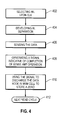
- FIG. 4 is a flow chart of the various steps involved in an exemplary memory cell reset operation in accordance with the teachings of the present invention.
- FIG. 1 depicted therein is a physical architectural view of a presently preferred exemplary embodiment of a CAM usage management system 100 wherein the teachings of the teachings of the present invention may be advantageously practiced.
- An exemplary CAM block 102 includes a CAM array 106 organized as N locations, each location preferably comprising a select width, e.g., a word.
- a CAM control block 110 is provided to direct an X-Decoder (XDEC) block 108 for generating appropriate row address signals (ADD- 0 through ADD-(N- 1 )) with respect to the N CAM locations.
- XDEC X-Decoder
- the array of CAM locations is addressed by providing a data value (i.e., search data) to each column of CAM cells via a suitable input/output (I/O) control block 112 .
- the CAM cells may be comprised of conventional twelve-transistor ( 12 -T) or nine-transistor ( 9 -T) cells (each cell being a static random access memory (SRAM) cell coupled to an exclusive-OR (XOR) gate) (not specifically shown in this FIG.).
- SRAM static random access memory
- XOR exclusive-OR
- complementary data values are also provided to the CAM columns.
- the CAM memory management system 100 provides a plurality of Match signals (Match- 0 through Match-(N- 1 )) that correspond to the N locations of CAM array 106 for determining whether or not the data of a location has changed since its storage thereat.
- the CAM array 106 For example, once the CAM array 106 is initialized, data can be searched through the entire CAM in a single search operation. If there is any match, the array can generate the address of the location (Match_Location) where the search data matches with the stored data. For maximum utilization of the CAM array and improved system performance, the array may be checked periodically whether the contents of the locations have changed since the previous check. If any location of the CAM array 106 is not used for valid data storage since the previous check (i.e., the contents of that location have changed and the corresponding Match signal is accordingly driven low during the search cycle), the location can be updated with new data.
- a separate memory 114 (referred to as an age_array) is provided for monitoring the CAM array usage.
- Age_array 114 is comprised of a plurality of cells (referred to as age_cells, Age Cell_ 0 through Age_Cell_N- 1 )) organized as an N-by-1 unidimensional array, wherein each cell corresponds to a particular location of the CAM array 106 and is set by the Match signal associated therewith.
- SA control/sense amp
- a control signal, Age_In 118 is applied as an input to the control/SA block 116 for effectuating the selection of a wordline (not shown in this FIG.) for a particular age_cell.
- a counter (age_counter) initialized with the size of the age_array 114 may be employed to generate at least a part of such control signal.
- An Age_Out signal 120 is available for outputting data read from a selected age_cell during a read operation with respect thereto.
- the functionality of the age_cells is to monitor if and when the CAM locations are available for new data storage.
- the age_array 114 is read (from one end to the other, using the age_counter, for example). Upon reading each age_cell, it is reset to 0.
- the corresponding age_cell is set to 1. Accordingly, when the age_array is 114 read again and the value of an age_cell is 0, it means that the particular age_cell has not been set to 1 by its Match signal during the CAM array search cycle. That is, the corresponding CAM location contains data that is no longer in use and, therefore, the location can be used for storing new data.
- conventional resetting of the age_array cells employs a separate write cycle following the read cycle for storing a binary 0 at a particular age_cell, which is wastefull of memory cycles and system resources.
- FIG. 2A depicts a presently preferred exemplary embodiment of a memory storage cell 200 A (such as an age_cell set forth hereinabove) including reset circuitry provided in accordance with the teachings of the present invention for storing a binary 0 without a separate write cycle.
- the memory storage cell 200 A includes a storage portion 202 comprised of an SRAM cell (e.g., 6-T cell) that can be read using a WL 210 associated therewith.
- Access transistors N 1 and N 2 are coupled to data (TRUE or T) and data bar (FALSE or F) nodes (reference numerals 206 and 208 , respectively) formed at the termini of a coupled inverter pair that is comprised of inverters 204 A and 204 B.
- Bitline (BT) 212 A and bitline bar (BB) 212 B are coupled to the data and data bar nodes via access transistors N 1 and N 2 , respectively.
- access transistors N 1 and N 2 access transistors
- the pair of bitline and bitline bar signals may be conventionally provided to a sense amp circuit for purposes of sensing data using well known techniques in the memory design art.
- a set/reset circuitry portion 203 is preferably provided as part of the memory storage cell 200 A for achieving combined setting and resetting functionality with respect to the storage portion 202 in accordance with the teachings of the present invention.
- Transistors N 3 and N 4 are coupled in series to the data node 206 , whereas transistor N 5 is coupled to the data bar node 208 .
- transistors N 3 , N 4 and N 5 are provided as n-channel MOS (NMOS) devices, wherein N 3 may be referred to as the discharge device, N 4 may be referred to as the pull-down device and N 5 may be referred to as the set device for the sake of convenience.
- NMOS n-channel MOS
- the WL signal 210 associated with the memory storage cell 200 A is provided to the gates of access transistors N 1 and N 2 as well as the gate of transistor N 3 .
- a Match signal 214 which corresponds to a particular CAM location (as described in detail hereinabove) is provided to the gate of transistor N 5 .
- a reset control signal 216 referred to as SA_END, is provided to the gate of transistor N 4 .
- WL 210 and SA_END 216 are inactive and Match signal 214 is driven high, provided a match condition is detected with respect to the corresponding CAM location. Accordingly, the set device N 5 is turned on and the data bar node 208 is pulled to ground. Thus, a binary value of 1 is stored at the data node 206 of the storage cell portion 202 .
- a sense amp block (e.g., SA block 116 depicted in FIG. 1) senses the voltage differential and stores the data value associated therewith for subsequent data out operations.
- the reset control signal 216 i.e., SA_END
- SA_END the reset control signal 216
- SA_END 216 is also provided to the address control block to deactivate the WL signal to complete the read cycle.
- the data value sensed by the SA is in the meantime outputted normally for subsequent operations.
- FIG. 2B depicts an exemplary embodiment of a semiconductor memory circuit 200 B comprising N memory storage cells (reference numerals 250 - 1 through 250 -N), each of which is preferably formed such as the memory storage cell 200 A described in detail hereinabove.
- the semiconductor memory circuit 200 B may preferably be operable as the age_array 114 shown in FIG. 1 .
- Each storage cell e.g., cell 250 - 1
- Each storage cell is comprised of a set port 252 , a reset port 254 , and a read/write port 256 .
- a main read/reset control circuitry 258 is provided for controlling read/write operations and reset operations with respect to the storage cell functionality as elucidated hereinabove.
- the read/write port 256 is operable with WL and Data In signals to sense data from and write data into the cell, respectively.
- the reset port 254 which is preferably activated only for the WL selected for a read operation with respect to a specific storage cell, is operable with a reset control signal (i.e, SA_END) for resetting the selected storage cell.
- SA_END reset control signal
- the reset control signal is also operable to deactivate the selected WL, wherein the reset path to the storage cell is faster than the reset path to the selected WL.
- the set port 252 of the memory storage cells (each of N rows having a set port) is preferably activatable by a Match signal emanating therefrom.
- FIG. 3 depicted therein is a timing diagram for the set/read/reset operations set forth above as exemplified with respect to the memory storage cell (or age cell) provided in accordance with the teachings of the present invention.
- WL and SA_END are inactive and Match 214 is driven high (exemplified by a rising edge 315 ).
- Data in the age_cell which is exemplified by AGE_CELL 304 , is set to 1 in response to the rising edge of the Match signal, as indicated by a rising edge 319 in AGE_CELL 304 .
- WL 210 Upon asserting a clock (CLK) signal 302 to indicate a read cycle (rising edge 308 in CLK), WL 210 is driven high (rising edge 310 ) responsive thereto.
- CLK clock
- WL 210 is driven high (rising edge 310 ) responsive thereto.
- the development of a voltage separation between BT and BB lines is exemplified by differential voltage 312 .
- Age_Out 120 is driven high (rising edge 314 ) to output the sensed data.
- SA_END 216 is asserted high (rising edge 316 ) which overlaps with the duration 322 when WL 210 is also high.
- VWL is deactivated (falling edge 320 ) and the data node is discharged as described in detail hereinabove.
- AGE_CELL 304 is accordingly driven low (exemplified by falling edge 318 ) to indicate storing of a binary 0.
- FIG. 4 is a flow chart of summarizing the various steps involved in the exemplary memory storage cell reset operation set forth above in accordance with the teachings of the present invention.
- a WL is selected (step 402 ) to initiate the read operation.
- Bitline separation is developed pursuant to the stored data value in the storage cell (step 404 ), which is subsequently sensed by SA circuitry (step 406 ).
- SA circuitry step 406
- a reset control signal indicative of the sensing operation condition is generated (step 408 ) and applied in accordance with the teachings herein in order to discharge the stored data.
- a binary 0 is therefore stored thereat without a dedicated write cycle therefor (step 410 ).
- This sequence of “built-in read/write” operations continues to take place thereafter for the next read cycle (step 412 ).
- the present invention provides a simple yet effective solution for advantageously eliminating dedicated write cycles in order to reset a memory.
- the present invention optimizes memory usage and system resources in a demanding application such as, e.g., network processors in routers, etc.
- the present invention is particularly advantageous with respect to more expensive memory such as CAM.
Abstract
Description
Claims (27)
Priority Applications (1)
| Application Number | Priority Date | Filing Date | Title |
|---|---|---|---|
| US09/706,314 US6466470B1 (en) | 2000-11-04 | 2000-11-04 | Circuitry and method for resetting memory without a write cycle |
Applications Claiming Priority (1)
| Application Number | Priority Date | Filing Date | Title |
|---|---|---|---|
| US09/706,314 US6466470B1 (en) | 2000-11-04 | 2000-11-04 | Circuitry and method for resetting memory without a write cycle |
Publications (1)
| Publication Number | Publication Date |
|---|---|
| US6466470B1 true US6466470B1 (en) | 2002-10-15 |
Family
ID=24837040
Family Applications (1)
| Application Number | Title | Priority Date | Filing Date |
|---|---|---|---|
| US09/706,314 Expired - Lifetime US6466470B1 (en) | 2000-11-04 | 2000-11-04 | Circuitry and method for resetting memory without a write cycle |
Country Status (1)
| Country | Link |
|---|---|
| US (1) | US6466470B1 (en) |
Cited By (12)
| Publication number | Priority date | Publication date | Assignee | Title |
|---|---|---|---|---|
| US20040017711A1 (en) * | 2002-03-27 | 2004-01-29 | Sung-Mo Kang | Self reverse bias low-power high-performance storage circuitry and related methods |
| US20050190639A1 (en) * | 2002-03-08 | 2005-09-01 | Hu Shane C. | Static content addressable memory cell |
| US20050190633A1 (en) * | 2001-05-22 | 2005-09-01 | The Regents Of The University Of California | Low-power high-performance integrated circuit and related methods |
| US20100030972A1 (en) * | 2008-07-29 | 2010-02-04 | Entropic Communications, Inc. | Device, system and method of accessing data stored in a memory. |
| US20150012757A1 (en) * | 2010-12-22 | 2015-01-08 | May Patents Ltd. | System and method for routing-based internet security |
| US9293193B2 (en) * | 2011-11-25 | 2016-03-22 | Semiconductor Energy Laboratory Co., Ltd. | Memory circuit and memory device |
| US9699193B2 (en) | 2013-07-03 | 2017-07-04 | Airwatch, Llc | Enterprise-specific functionality watermarking and management |
| US9703949B2 (en) | 2013-05-02 | 2017-07-11 | Airwatch, Llc | Time-based configuration profile toggling |
| US10069936B2 (en) | 2009-10-08 | 2018-09-04 | Hola Newco Ltd. | System providing faster and more efficient data communication |
| US10277711B2 (en) | 2013-08-28 | 2019-04-30 | Luminati Networks Ltd. | System and method for improving internet communication by using intermediate nodes |
| US10616294B2 (en) | 2015-05-14 | 2020-04-07 | Web Spark Ltd. | System and method for streaming content from multiple servers |
| US11956299B2 (en) | 2023-09-27 | 2024-04-09 | Bright Data Ltd. | System providing faster and more efficient data communication |
Citations (9)
| Publication number | Priority date | Publication date | Assignee | Title |
|---|---|---|---|---|
| US627788A (en) * | 1898-12-27 | 1899-06-27 | Anthony Wayne Mfg Company | Washing-machine. |
| US5226009A (en) * | 1990-03-30 | 1993-07-06 | Mitsubishi Denki Kabushiki Kaisha | Semiconductor memory device supporting cache and method of driving the same |
| US5325325A (en) * | 1990-03-30 | 1994-06-28 | Sharp Kabushiki Kaisha | Semiconductor memory device capable of initializing storage data |
| US5790461A (en) * | 1995-01-12 | 1998-08-04 | Intergraph Corporation | Register file with bypass capability |
| US5894432A (en) * | 1997-07-08 | 1999-04-13 | International Business Machines Corporation | CMOS memory cell with improved read port |
| US5999478A (en) * | 1998-05-21 | 1999-12-07 | Integrated Device Technology, Inc. | Highly integrated tri-port memory buffers having fast fall-through capability and methods of operating same |
| US6108233A (en) * | 1999-08-27 | 2000-08-22 | Lucent Technologies Inc. | Ultra low voltage static RAM memory cell |
| US6122707A (en) | 1997-09-04 | 2000-09-19 | Nortel Networks Corporation | Content addressable memory system with self-timed signals and cascaded memories for propagating hit signals |
| US6128207A (en) | 1998-11-02 | 2000-10-03 | Integrated Device Technology, Inc. | Low-power content addressable memory cell |
-
2000
- 2000-11-04 US US09/706,314 patent/US6466470B1/en not_active Expired - Lifetime
Patent Citations (9)
| Publication number | Priority date | Publication date | Assignee | Title |
|---|---|---|---|---|
| US627788A (en) * | 1898-12-27 | 1899-06-27 | Anthony Wayne Mfg Company | Washing-machine. |
| US5226009A (en) * | 1990-03-30 | 1993-07-06 | Mitsubishi Denki Kabushiki Kaisha | Semiconductor memory device supporting cache and method of driving the same |
| US5325325A (en) * | 1990-03-30 | 1994-06-28 | Sharp Kabushiki Kaisha | Semiconductor memory device capable of initializing storage data |
| US5790461A (en) * | 1995-01-12 | 1998-08-04 | Intergraph Corporation | Register file with bypass capability |
| US5894432A (en) * | 1997-07-08 | 1999-04-13 | International Business Machines Corporation | CMOS memory cell with improved read port |
| US6122707A (en) | 1997-09-04 | 2000-09-19 | Nortel Networks Corporation | Content addressable memory system with self-timed signals and cascaded memories for propagating hit signals |
| US5999478A (en) * | 1998-05-21 | 1999-12-07 | Integrated Device Technology, Inc. | Highly integrated tri-port memory buffers having fast fall-through capability and methods of operating same |
| US6128207A (en) | 1998-11-02 | 2000-10-03 | Integrated Device Technology, Inc. | Low-power content addressable memory cell |
| US6108233A (en) * | 1999-08-27 | 2000-08-22 | Lucent Technologies Inc. | Ultra low voltage static RAM memory cell |
Non-Patent Citations (1)
| Title |
|---|
| Content Addressable Memory Structures, IBM Technique Disclosure Bulletin, Mar. 1989 US, vol. 31, pp. 461-466. * |
Cited By (129)
| Publication number | Priority date | Publication date | Assignee | Title |
|---|---|---|---|---|
| US20050190633A1 (en) * | 2001-05-22 | 2005-09-01 | The Regents Of The University Of California | Low-power high-performance integrated circuit and related methods |
| US7190209B2 (en) | 2001-05-22 | 2007-03-13 | The Regents Of The University Of California | Low-power high-performance integrated circuit and related methods |
| US20050190639A1 (en) * | 2002-03-08 | 2005-09-01 | Hu Shane C. | Static content addressable memory cell |
| US20060114705A1 (en) * | 2002-03-08 | 2006-06-01 | Hu Shane C | Static content addressable memory cell |
| US20060181911A1 (en) * | 2002-03-08 | 2006-08-17 | Hu Shane C | Static content addressable memory cell |
| US7099172B2 (en) * | 2002-03-08 | 2006-08-29 | Micron Technology, Inc. | Static content addressable memory cell |
| US7269040B2 (en) | 2002-03-08 | 2007-09-11 | Micron Technology, Inc. | Static content addressable memory cell |
| US7307860B2 (en) | 2002-03-08 | 2007-12-11 | Micron Technology, Inc. | Static content addressable memory cell |
| US20040017711A1 (en) * | 2002-03-27 | 2004-01-29 | Sung-Mo Kang | Self reverse bias low-power high-performance storage circuitry and related methods |
| US9514060B2 (en) * | 2008-07-29 | 2016-12-06 | Entropic Communications, Llc | Device, system and method of accessing data stored in a memory |
| US20100030972A1 (en) * | 2008-07-29 | 2010-02-04 | Entropic Communications, Inc. | Device, system and method of accessing data stored in a memory. |
| US20170147508A1 (en) * | 2008-07-29 | 2017-05-25 | Entropic Communications, Llc | Device, system and method of accessing data stored in a memory |
| US11659017B2 (en) | 2009-10-08 | 2023-05-23 | Bright Data Ltd. | System providing faster and more efficient data communication |
| US11190622B2 (en) | 2009-10-08 | 2021-11-30 | Bright Data Ltd. | System providing faster and more efficient data communication |
| US11949729B2 (en) | 2009-10-08 | 2024-04-02 | Bright Data Ltd. | System providing faster and more efficient data communication |
| US11916993B2 (en) | 2009-10-08 | 2024-02-27 | Bright Data Ltd. | System providing faster and more efficient data communication |
| US11902351B2 (en) | 2009-10-08 | 2024-02-13 | Bright Data Ltd. | System providing faster and more efficient data communication |
| US10069936B2 (en) | 2009-10-08 | 2018-09-04 | Hola Newco Ltd. | System providing faster and more efficient data communication |
| US10225374B2 (en) | 2009-10-08 | 2019-03-05 | Hola Newco Ltd. | System providing faster and more efficient data communication |
| US10257319B2 (en) | 2009-10-08 | 2019-04-09 | Web Spark Ltd. | System providing faster and more efficient data communication |
| US11888922B2 (en) | 2009-10-08 | 2024-01-30 | Bright Data Ltd. | System providing faster and more efficient data communication |
| US10313484B2 (en) | 2009-10-08 | 2019-06-04 | Web Spark Ltd. | System providing faster and more efficient data communication |
| US11888921B2 (en) | 2009-10-08 | 2024-01-30 | Bright Data Ltd. | System providing faster and more efficient data communication |
| US11876853B2 (en) | 2009-10-08 | 2024-01-16 | Bright Data Ltd. | System providing faster and more efficient data communication |
| US10469628B2 (en) | 2009-10-08 | 2019-11-05 | Web Spark Ltd. | System providing faster and more efficient data communication |
| US11838119B2 (en) | 2009-10-08 | 2023-12-05 | Bright Data Ltd. | System providing faster and more efficient data communication |
| US11811849B2 (en) | 2009-10-08 | 2023-11-07 | Bright Data Ltd. | System providing faster and more efficient data communication |
| US10484510B2 (en) | 2009-10-08 | 2019-11-19 | Web Spark Ltd. | System providing faster and more efficient data communication |
| US10484511B2 (en) | 2009-10-08 | 2019-11-19 | Web Spark Ltd. | System providing faster and more efficient data communication |
| US10491712B2 (en) | 2009-10-08 | 2019-11-26 | Web Spark Ltd. | System providing faster and more efficient data communication |
| US10491713B2 (en) | 2009-10-08 | 2019-11-26 | Web Spark Ltd. | System providing faster and more efficient data communication |
| US10523788B2 (en) | 2009-10-08 | 2019-12-31 | Web Sparks Ltd. | System providing faster and more efficient data communication |
| US11233880B2 (en) | 2009-10-08 | 2022-01-25 | Bright Data Ltd. | System providing faster and more efficient data communication |
| US10582013B2 (en) | 2009-10-08 | 2020-03-03 | Luminati Networks Ltd. | System providing faster and more efficient data communication |
| US11811850B2 (en) | 2009-10-08 | 2023-11-07 | Bright Data Ltd. | System providing faster and more efficient data communication |
| US10616375B2 (en) | 2009-10-08 | 2020-04-07 | Luminati Networks Ltd. | System providing faster and more efficient data communication |
| US10637968B2 (en) | 2009-10-08 | 2020-04-28 | Luminati Networks Ltd. | System providing faster and more efficient data communication |
| US11811848B2 (en) | 2009-10-08 | 2023-11-07 | Bright Data Ltd. | System providing faster and more efficient data communication |
| US11770435B2 (en) | 2009-10-08 | 2023-09-26 | Bright Data Ltd. | System providing faster and more efficient data communication |
| US11700295B2 (en) | 2009-10-08 | 2023-07-11 | Bright Data Ltd. | System providing faster and more efficient data communication |
| US11671476B2 (en) | 2009-10-08 | 2023-06-06 | Bright Data Ltd. | System providing faster and more efficient data communication |
| US11659018B2 (en) | 2009-10-08 | 2023-05-23 | Bright Data Ltd. | System providing faster and more efficient data communication |
| US10785347B1 (en) | 2009-10-08 | 2020-09-22 | Luminati Networks Ltd. | System providing faster and more efficient data communication |
| US10805429B1 (en) | 2009-10-08 | 2020-10-13 | Luminati Networks Ltd. | System providing faster and more efficient data communication |
| US11616826B2 (en) | 2009-10-08 | 2023-03-28 | Bright Data Ltd. | System providing faster and more efficient data communication |
| US10931792B2 (en) | 2009-10-08 | 2021-02-23 | Luminati Networks Ltd. | System providing faster and more efficient data communication |
| US10958768B1 (en) | 2009-10-08 | 2021-03-23 | Luminati Networks Ltd. | System providing faster and more efficient data communication |
| US11611607B2 (en) | 2009-10-08 | 2023-03-21 | Bright Data Ltd. | System providing faster and more efficient data communication |
| US11539779B2 (en) | 2009-10-08 | 2022-12-27 | Bright Data Ltd. | System providing faster and more efficient data communication |
| US10986216B2 (en) | 2009-10-08 | 2021-04-20 | Luminati Networks Ltd. | System providing faster and more efficient data communication |
| US11457058B2 (en) | 2009-10-08 | 2022-09-27 | Bright Data Ltd. | System providing faster and more efficient data communication |
| US11412025B2 (en) | 2009-10-08 | 2022-08-09 | Bright Data Ltd. | System providing faster and more efficient data communication |
| US11303734B2 (en) | 2009-10-08 | 2022-04-12 | Bright Data Ltd. | System providing faster and more efficient data communication |
| US11297167B2 (en) | 2009-10-08 | 2022-04-05 | Bright Data Ltd. | System providing faster and more efficient data communication |
| US11038989B2 (en) | 2009-10-08 | 2021-06-15 | Bright Data Ltd. | System providing faster and more efficient data communication |
| US11044341B2 (en) | 2009-10-08 | 2021-06-22 | Bright Data Ltd. | System providing faster and more efficient data communication |
| US11044342B2 (en) | 2009-10-08 | 2021-06-22 | Bright Data Ltd. | System providing faster and more efficient data communication |
| US11044346B2 (en) | 2009-10-08 | 2021-06-22 | Bright Data Ltd. | System providing faster and more efficient data communication |
| US11044345B2 (en) | 2009-10-08 | 2021-06-22 | Bright Data Ltd. | System providing faster and more efficient data communication |
| US11044344B2 (en) | 2009-10-08 | 2021-06-22 | Bright Data Ltd. | System providing faster and more efficient data communication |
| US11050852B2 (en) | 2009-10-08 | 2021-06-29 | Bright Data Ltd. | System providing faster and more efficient data communication |
| US11233881B2 (en) | 2009-10-08 | 2022-01-25 | Bright Data Ltd. | System providing faster and more efficient data communication |
| US11089135B2 (en) | 2009-10-08 | 2021-08-10 | Bright Data Ltd. | System providing faster and more efficient data communication |
| US11233879B2 (en) | 2009-10-08 | 2022-01-25 | Bright Data Ltd. | System providing faster and more efficient data communication |
| US11128738B2 (en) | 2009-10-08 | 2021-09-21 | Bright Data Ltd. | Fetching content from multiple web servers using an intermediate client device |
| US10582014B2 (en) | 2009-10-08 | 2020-03-03 | Luminati Networks Ltd. | System providing faster and more efficient data communication |
| US11178258B2 (en) | 2009-10-08 | 2021-11-16 | Bright Data Ltd. | System providing faster and more efficient data communication |
| US11228666B2 (en) | 2009-10-08 | 2022-01-18 | Bright Data Ltd. | System providing faster and more efficient data communication |
| US11206317B2 (en) | 2009-10-08 | 2021-12-21 | Bright Data Ltd. | System providing faster and more efficient data communication |
| US11303612B2 (en) | 2010-12-22 | 2022-04-12 | May Patents Ltd. | System and method for routing-based internet security |
| US9762547B2 (en) * | 2010-12-22 | 2017-09-12 | May Patents Ltd. | System and method for routing-based internet security |
| US11876785B2 (en) | 2010-12-22 | 2024-01-16 | May Patents Ltd. | System and method for routing-based internet security |
| US10652214B2 (en) | 2010-12-22 | 2020-05-12 | May Patents Ltd. | System and method for routing-based internet security |
| US20150012757A1 (en) * | 2010-12-22 | 2015-01-08 | May Patents Ltd. | System and method for routing-based internet security |
| US9293193B2 (en) * | 2011-11-25 | 2016-03-22 | Semiconductor Energy Laboratory Co., Ltd. | Memory circuit and memory device |
| US9703949B2 (en) | 2013-05-02 | 2017-07-11 | Airwatch, Llc | Time-based configuration profile toggling |
| US9699193B2 (en) | 2013-07-03 | 2017-07-04 | Airwatch, Llc | Enterprise-specific functionality watermarking and management |
| US11949756B2 (en) | 2013-08-28 | 2024-04-02 | Bright Data Ltd. | System and method for improving internet communication by using intermediate nodes |
| US10721325B2 (en) | 2013-08-28 | 2020-07-21 | Luminati Networks Ltd. | System and method for improving internet communication by using intermediate nodes |
| US11310341B2 (en) | 2013-08-28 | 2022-04-19 | Bright Data Ltd. | System and method for improving internet communication by using intermediate nodes |
| US11316950B2 (en) | 2013-08-28 | 2022-04-26 | Bright Data Ltd. | System and method for improving internet communication by using intermediate nodes |
| US11336745B2 (en) | 2013-08-28 | 2022-05-17 | Bright Data Ltd. | System and method for improving internet communication by using intermediate nodes |
| US11336746B2 (en) | 2013-08-28 | 2022-05-17 | Bright Data Ltd. | System and method for improving Internet communication by using intermediate nodes |
| US11349953B2 (en) | 2013-08-28 | 2022-05-31 | Bright Data Ltd. | System and method for improving internet communication by using intermediate nodes |
| US11388257B2 (en) | 2013-08-28 | 2022-07-12 | Bright Data Ltd. | System and method for improving internet communication by using intermediate nodes |
| US11412066B2 (en) | 2013-08-28 | 2022-08-09 | Bright Data Ltd. | System and method for improving internet communication by using intermediate nodes |
| US11005967B2 (en) | 2013-08-28 | 2021-05-11 | Bright Data Ltd. | System and method for improving internet communication by using intermediate nodes |
| US11451640B2 (en) | 2013-08-28 | 2022-09-20 | Bright Data Ltd. | System and method for improving internet communication by using intermediate nodes |
| US10999402B2 (en) | 2013-08-28 | 2021-05-04 | Bright Data Ltd. | System and method for improving internet communication by using intermediate nodes |
| US10986208B2 (en) | 2013-08-28 | 2021-04-20 | Luminati Networks Ltd. | System and method for improving internet communication by using intermediate nodes |
| US11575771B2 (en) | 2013-08-28 | 2023-02-07 | Bright Data Ltd. | System and method for improving internet communication by using intermediate nodes |
| US11588920B2 (en) | 2013-08-28 | 2023-02-21 | Bright Data Ltd. | System and method for improving internet communication by using intermediate nodes |
| US11595497B2 (en) | 2013-08-28 | 2023-02-28 | Bright Data Ltd. | System and method for improving internet communication by using intermediate nodes |
| US11595496B2 (en) | 2013-08-28 | 2023-02-28 | Bright Data Ltd. | System and method for improving internet communication by using intermediate nodes |
| US10979533B2 (en) | 2013-08-28 | 2021-04-13 | Luminati Networks Ltd. | System and method for improving internet communication by using intermediate nodes |
| US10924580B2 (en) | 2013-08-28 | 2021-02-16 | Luminati Networks Ltd. | System and method for improving internet communication by using intermediate nodes |
| US11632439B2 (en) | 2013-08-28 | 2023-04-18 | Bright Data Ltd. | System and method for improving internet communication by using intermediate nodes |
| US11012529B2 (en) | 2013-08-28 | 2021-05-18 | Luminati Networks Ltd. | System and method for improving internet communication by using intermediate nodes |
| US11677856B2 (en) | 2013-08-28 | 2023-06-13 | Bright Data Ltd. | System and method for improving internet communication by using intermediate nodes |
| US11233872B2 (en) | 2013-08-28 | 2022-01-25 | Bright Data Ltd. | System and method for improving internet communication by using intermediate nodes |
| US11012530B2 (en) | 2013-08-28 | 2021-05-18 | Bright Data Ltd. | System and method for improving internet communication by using intermediate nodes |
| US11689639B2 (en) | 2013-08-28 | 2023-06-27 | Bright Data Ltd. | System and method for improving Internet communication by using intermediate nodes |
| US11303724B2 (en) | 2013-08-28 | 2022-04-12 | Bright Data Ltd. | System and method for improving internet communication by using intermediate nodes |
| US11729297B2 (en) | 2013-08-28 | 2023-08-15 | Bright Data Ltd. | System and method for improving internet communication by using intermediate nodes |
| US11178250B2 (en) | 2013-08-28 | 2021-11-16 | Bright Data Ltd. | System and method for improving internet communication by using intermediate nodes |
| US11758018B2 (en) | 2013-08-28 | 2023-09-12 | Bright Data Ltd. | System and method for improving internet communication by using intermediate nodes |
| US10652357B2 (en) | 2013-08-28 | 2020-05-12 | Luminati Networks Ltd. | System and method for improving internet communication by using intermediate nodes |
| US10659562B2 (en) | 2013-08-28 | 2020-05-19 | Luminati Networks Ltd. | System and method for improving internet communication by using intermediate nodes |
| US11799985B2 (en) | 2013-08-28 | 2023-10-24 | Bright Data Ltd. | System and method for improving internet communication by using intermediate nodes |
| US10652358B2 (en) | 2013-08-28 | 2020-05-12 | Luminati Networks Ltd. | System and method for improving internet communication by using intermediate nodes |
| US11949755B2 (en) | 2013-08-28 | 2024-04-02 | Bright Data Ltd. | System and method for improving internet communication by using intermediate nodes |
| US10469614B2 (en) | 2013-08-28 | 2019-11-05 | Luminati Networks Ltd. | System and method for improving Internet communication by using intermediate nodes |
| US11838386B2 (en) | 2013-08-28 | 2023-12-05 | Bright Data Ltd. | System and method for improving internet communication by using intermediate nodes |
| US10469615B2 (en) | 2013-08-28 | 2019-11-05 | Luminati Networks Ltd. | System and method for improving internet communication by using intermediate nodes |
| US11838388B2 (en) | 2013-08-28 | 2023-12-05 | Bright Data Ltd. | System and method for improving internet communication by using intermediate nodes |
| US11870874B2 (en) | 2013-08-28 | 2024-01-09 | Bright Data Ltd. | System and method for improving internet communication by using intermediate nodes |
| US11924307B2 (en) | 2013-08-28 | 2024-03-05 | Bright Data Ltd. | System and method for improving internet communication by using intermediate nodes |
| US10447809B2 (en) | 2013-08-28 | 2019-10-15 | Luminati Networks Ltd. | System and method for improving internet communication by using intermediate nodes |
| US10440146B2 (en) | 2013-08-28 | 2019-10-08 | Luminati Networks Ltd. | System and method for improving internet communication by using intermediate nodes |
| US10277711B2 (en) | 2013-08-28 | 2019-04-30 | Luminati Networks Ltd. | System and method for improving internet communication by using intermediate nodes |
| US11902400B2 (en) | 2013-08-28 | 2024-02-13 | Bright Data Ltd. | System and method for improving internet communication by using intermediate nodes |
| US11102326B2 (en) | 2013-08-28 | 2021-08-24 | Bright Data Ltd. | System and method for improving internet communication by using intermediate nodes |
| US11272034B2 (en) | 2013-08-28 | 2022-03-08 | Bright Data Ltd. | System and method for improving internet communication by using intermediate nodes |
| US11924306B2 (en) | 2013-08-28 | 2024-03-05 | Bright Data Ltd. | System and method for improving internet communication by using intermediate nodes |
| US11057446B2 (en) | 2015-05-14 | 2021-07-06 | Bright Data Ltd. | System and method for streaming content from multiple servers |
| US10616294B2 (en) | 2015-05-14 | 2020-04-07 | Web Spark Ltd. | System and method for streaming content from multiple servers |
| US11770429B2 (en) | 2015-05-14 | 2023-09-26 | Bright Data Ltd. | System and method for streaming content from multiple servers |
| US11757961B2 (en) | 2015-05-14 | 2023-09-12 | Bright Data Ltd. | System and method for streaming content from multiple servers |
| US11956299B2 (en) | 2023-09-27 | 2024-04-09 | Bright Data Ltd. | System providing faster and more efficient data communication |
Similar Documents
| Publication | Publication Date | Title |
|---|---|---|
| US5646878A (en) | Content addressable memory system | |
| US6081441A (en) | Content-addressable memory | |
| US6381673B1 (en) | Method and apparatus for performing a read next highest priority match instruction in a content addressable memory device | |
| EP0905709B1 (en) | Single ended match sense amplifier | |
| US6252814B1 (en) | Dummy wordline circuitry | |
| US6597596B2 (en) | Content addressable memory having cascaded sub-entry architecture | |
| US4930104A (en) | Content-addressed memory | |
| US6317351B2 (en) | Associative cache memory capable of reconfiguring a K-way and N-set cache memory into a M-unit, K-way and N/M-set cache memory | |
| US5991191A (en) | Methods and circuits for single-memory cell multivalue data storage | |
| US6466470B1 (en) | Circuitry and method for resetting memory without a write cycle | |
| JPH04325996A (en) | Associated semiconductor memory device | |
| JPH07312085A (en) | Memory device | |
| US5745421A (en) | Method and apparatus for self-timed precharge of bit lines in a memory | |
| US5668766A (en) | Method and apparatus for increasing memory read access speed using double-sensing | |
| US6172925B1 (en) | Memory array bitline timing circuit | |
| US5619464A (en) | High performance RAM array circuit employing self-time clock generator for enabling array accessess | |
| US7606054B2 (en) | Cache hit logic of cache memory and processor chip having the same | |
| US5724294A (en) | Self-tracking sense amplifier strobing circuit and method | |
| US5761700A (en) | ROM mapping and inversion apparatus and method | |
| US20040228155A1 (en) | Folded dram cam cell | |
| US7376038B2 (en) | Fast access memory architecture | |
| US5732255A (en) | Signal processing system with ROM storing instructions encoded for reducing power consumpton during reads and method for encoding such instructions | |
| US5592426A (en) | Extended segmented precharge architecture | |
| KR950020173A (en) | Data processing system with memory with low power operation mode and method thereof | |
| US7342814B2 (en) | Content addressable memory with reduced search current and power |
Legal Events
| Date | Code | Title | Description |
|---|---|---|---|
| AS | Assignment |
Owner name: VIRAGE LOGIC CORP., CALIFORNIA Free format text: ASSIGNMENT OF ASSIGNORS INTEREST;ASSIGNOR:CHANG, HOUN;REEL/FRAME:011282/0673 Effective date: 20001018 |
|
| STCF | Information on status: patent grant |
Free format text: PATENTED CASE |
|
| FPAY | Fee payment |
Year of fee payment: 4 |
|
| FPAY | Fee payment |
Year of fee payment: 8 |
|
| AS | Assignment |
Owner name: SYNOPSYS, INC., CALIFORNIA Free format text: ASSIGNMENT OF ASSIGNORS INTEREST;ASSIGNORS:VIRAGE LOGIC CORPORATION;VL C.V.;ARC CORES LIMITED;AND OTHERS;REEL/FRAME:025105/0907 Effective date: 20100902 |
|
| FEPP | Fee payment procedure |
Free format text: PAYER NUMBER DE-ASSIGNED (ORIGINAL EVENT CODE: RMPN); ENTITY STATUS OF PATENT OWNER: LARGE ENTITY Free format text: PAYOR NUMBER ASSIGNED (ORIGINAL EVENT CODE: ASPN); ENTITY STATUS OF PATENT OWNER: LARGE ENTITY |
|
| FEPP | Fee payment procedure |
Free format text: PAT HOLDER NO LONGER CLAIMS SMALL ENTITY STATUS, ENTITY STATUS SET TO UNDISCOUNTED (ORIGINAL EVENT CODE: STOL); ENTITY STATUS OF PATENT OWNER: LARGE ENTITY |
|
| REFU | Refund |
Free format text: REFUND - PAYMENT OF MAINTENANCE FEE, 12TH YR, SMALL ENTITY (ORIGINAL EVENT CODE: R2553); ENTITY STATUS OF PATENT OWNER: LARGE ENTITY |
|
| FPAY | Fee payment |
Year of fee payment: 12 |