US6469374B1 - Superposed printed substrates and insulating substrates having semiconductor elements inside - Google Patents
Superposed printed substrates and insulating substrates having semiconductor elements inside Download PDFInfo
- Publication number
- US6469374B1 US6469374B1 US09/648,373 US64837300A US6469374B1 US 6469374 B1 US6469374 B1 US 6469374B1 US 64837300 A US64837300 A US 64837300A US 6469374 B1 US6469374 B1 US 6469374B1
- Authority
- US
- United States
- Prior art keywords
- substrate
- conductive
- insulating substrate
- superposed
- provided insulating
- Prior art date
- Legal status (The legal status is an assumption and is not a legal conclusion. Google has not performed a legal analysis and makes no representation as to the accuracy of the status listed.)
- Expired - Lifetime
Links
- 239000000758 substrate Substances 0.000 title claims abstract description 427
- 239000004065 semiconductor Substances 0.000 title claims abstract description 235
- 239000004020 conductor Substances 0.000 claims abstract description 44
- 239000000853 adhesive Substances 0.000 claims description 45
- 238000004519 manufacturing process Methods 0.000 description 51
- RYGMFSIKBFXOCR-UHFFFAOYSA-N Copper Chemical compound [Cu] RYGMFSIKBFXOCR-UHFFFAOYSA-N 0.000 description 37
- 239000011889 copper foil Substances 0.000 description 30
- 238000000034 method Methods 0.000 description 16
- 239000004642 Polyimide Substances 0.000 description 12
- 229920001721 polyimide Polymers 0.000 description 12
- 229920002050 silicone resin Polymers 0.000 description 10
- 229910052802 copper Inorganic materials 0.000 description 7
- 239000010949 copper Substances 0.000 description 7
- 239000000463 material Substances 0.000 description 6
- 230000008901 benefit Effects 0.000 description 5
- CURLTUGMZLYLDI-UHFFFAOYSA-N Carbon dioxide Chemical compound O=C=O CURLTUGMZLYLDI-UHFFFAOYSA-N 0.000 description 4
- 239000003822 epoxy resin Substances 0.000 description 4
- 239000000945 filler Substances 0.000 description 4
- 229920000647 polyepoxide Polymers 0.000 description 4
- 229920001187 thermosetting polymer Polymers 0.000 description 4
- XUIMIQQOPSSXEZ-UHFFFAOYSA-N Silicon Chemical compound [Si] XUIMIQQOPSSXEZ-UHFFFAOYSA-N 0.000 description 3
- 229920001971 elastomer Polymers 0.000 description 3
- 239000000806 elastomer Substances 0.000 description 3
- PCHJSUWPFVWCPO-UHFFFAOYSA-N gold Chemical compound [Au] PCHJSUWPFVWCPO-UHFFFAOYSA-N 0.000 description 3
- 229910052737 gold Inorganic materials 0.000 description 3
- 239000010931 gold Substances 0.000 description 3
- BQCADISMDOOEFD-UHFFFAOYSA-N Silver Chemical compound [Ag] BQCADISMDOOEFD-UHFFFAOYSA-N 0.000 description 2
- XAGFODPZIPBFFR-UHFFFAOYSA-N aluminium Chemical compound [Al] XAGFODPZIPBFFR-UHFFFAOYSA-N 0.000 description 2
- 229910052782 aluminium Inorganic materials 0.000 description 2
- 229910002092 carbon dioxide Inorganic materials 0.000 description 2
- 239000001569 carbon dioxide Substances 0.000 description 2
- 230000000694 effects Effects 0.000 description 2
- 238000010438 heat treatment Methods 0.000 description 2
- 230000010354 integration Effects 0.000 description 2
- 238000012986 modification Methods 0.000 description 2
- 230000004048 modification Effects 0.000 description 2
- 229920005989 resin Polymers 0.000 description 2
- 239000011347 resin Substances 0.000 description 2
- 229910052709 silver Inorganic materials 0.000 description 2
- 239000004332 silver Substances 0.000 description 2
- 239000002313 adhesive film Substances 0.000 description 1
- 230000015572 biosynthetic process Effects 0.000 description 1
- 238000007796 conventional method Methods 0.000 description 1
- 239000011888 foil Substances 0.000 description 1
- 229910052710 silicon Inorganic materials 0.000 description 1
- 239000010703 silicon Substances 0.000 description 1
- 238000005476 soldering Methods 0.000 description 1
- 125000006850 spacer group Chemical group 0.000 description 1
Images


Classifications
-
- H—ELECTRICITY
- H01—ELECTRIC ELEMENTS
- H01L—SEMICONDUCTOR DEVICES NOT COVERED BY CLASS H10
- H01L23/00—Details of semiconductor or other solid state devices
- H01L23/12—Mountings, e.g. non-detachable insulating substrates
-
- H—ELECTRICITY
- H01—ELECTRIC ELEMENTS
- H01L—SEMICONDUCTOR DEVICES NOT COVERED BY CLASS H10
- H01L23/00—Details of semiconductor or other solid state devices
- H01L23/48—Arrangements for conducting electric current to or from the solid state body in operation, e.g. leads, terminal arrangements ; Selection of materials therefor
- H01L23/488—Arrangements for conducting electric current to or from the solid state body in operation, e.g. leads, terminal arrangements ; Selection of materials therefor consisting of soldered or bonded constructions
- H01L23/498—Leads, i.e. metallisations or lead-frames on insulating substrates, e.g. chip carriers
- H01L23/49833—Leads, i.e. metallisations or lead-frames on insulating substrates, e.g. chip carriers the chip support structure consisting of a plurality of insulating substrates
-
- H—ELECTRICITY
- H01—ELECTRIC ELEMENTS
- H01L—SEMICONDUCTOR DEVICES NOT COVERED BY CLASS H10
- H01L24/00—Arrangements for connecting or disconnecting semiconductor or solid-state bodies; Methods or apparatus related thereto
- H01L24/93—Batch processes
- H01L24/95—Batch processes at chip-level, i.e. with connecting carried out on a plurality of singulated devices, i.e. on diced chips
- H01L24/97—Batch processes at chip-level, i.e. with connecting carried out on a plurality of singulated devices, i.e. on diced chips the devices being connected to a common substrate, e.g. interposer, said common substrate being separable into individual assemblies after connecting
-
- H—ELECTRICITY
- H01—ELECTRIC ELEMENTS
- H01L—SEMICONDUCTOR DEVICES NOT COVERED BY CLASS H10
- H01L25/00—Assemblies consisting of a plurality of individual semiconductor or other solid state devices ; Multistep manufacturing processes thereof
- H01L25/03—Assemblies consisting of a plurality of individual semiconductor or other solid state devices ; Multistep manufacturing processes thereof all the devices being of a type provided for in the same subgroup of groups H01L27/00 - H01L33/00, or in a single subclass of H10K, H10N, e.g. assemblies of rectifier diodes
- H01L25/10—Assemblies consisting of a plurality of individual semiconductor or other solid state devices ; Multistep manufacturing processes thereof all the devices being of a type provided for in the same subgroup of groups H01L27/00 - H01L33/00, or in a single subclass of H10K, H10N, e.g. assemblies of rectifier diodes the devices having separate containers
- H01L25/105—Assemblies consisting of a plurality of individual semiconductor or other solid state devices ; Multistep manufacturing processes thereof all the devices being of a type provided for in the same subgroup of groups H01L27/00 - H01L33/00, or in a single subclass of H10K, H10N, e.g. assemblies of rectifier diodes the devices having separate containers the devices being of a type provided for in group H01L27/00
-
- H—ELECTRICITY
- H01—ELECTRIC ELEMENTS
- H01L—SEMICONDUCTOR DEVICES NOT COVERED BY CLASS H10
- H01L2224/00—Indexing scheme for arrangements for connecting or disconnecting semiconductor or solid-state bodies and methods related thereto as covered by H01L24/00
- H01L2224/01—Means for bonding being attached to, or being formed on, the surface to be connected, e.g. chip-to-package, die-attach, "first-level" interconnects; Manufacturing methods related thereto
- H01L2224/10—Bump connectors; Manufacturing methods related thereto
- H01L2224/15—Structure, shape, material or disposition of the bump connectors after the connecting process
- H01L2224/16—Structure, shape, material or disposition of the bump connectors after the connecting process of an individual bump connector
-
- H—ELECTRICITY
- H01—ELECTRIC ELEMENTS
- H01L—SEMICONDUCTOR DEVICES NOT COVERED BY CLASS H10
- H01L2225/00—Details relating to assemblies covered by the group H01L25/00 but not provided for in its subgroups
- H01L2225/03—All the devices being of a type provided for in the same subgroup of groups H01L27/00 - H01L33/648 and H10K99/00
- H01L2225/10—All the devices being of a type provided for in the same subgroup of groups H01L27/00 - H01L33/648 and H10K99/00 the devices having separate containers
- H01L2225/1005—All the devices being of a type provided for in the same subgroup of groups H01L27/00 - H01L33/648 and H10K99/00 the devices having separate containers the devices being of a type provided for in group H01L27/00
- H01L2225/1011—All the devices being of a type provided for in the same subgroup of groups H01L27/00 - H01L33/648 and H10K99/00 the devices having separate containers the devices being of a type provided for in group H01L27/00 the containers being in a stacked arrangement
- H01L2225/1017—All the devices being of a type provided for in the same subgroup of groups H01L27/00 - H01L33/648 and H10K99/00 the devices having separate containers the devices being of a type provided for in group H01L27/00 the containers being in a stacked arrangement the lowermost container comprising a device support
- H01L2225/1023—All the devices being of a type provided for in the same subgroup of groups H01L27/00 - H01L33/648 and H10K99/00 the devices having separate containers the devices being of a type provided for in group H01L27/00 the containers being in a stacked arrangement the lowermost container comprising a device support the support being an insulating substrate
-
- H—ELECTRICITY
- H01—ELECTRIC ELEMENTS
- H01L—SEMICONDUCTOR DEVICES NOT COVERED BY CLASS H10
- H01L2225/00—Details relating to assemblies covered by the group H01L25/00 but not provided for in its subgroups
- H01L2225/03—All the devices being of a type provided for in the same subgroup of groups H01L27/00 - H01L33/648 and H10K99/00
- H01L2225/10—All the devices being of a type provided for in the same subgroup of groups H01L27/00 - H01L33/648 and H10K99/00 the devices having separate containers
- H01L2225/1005—All the devices being of a type provided for in the same subgroup of groups H01L27/00 - H01L33/648 and H10K99/00 the devices having separate containers the devices being of a type provided for in group H01L27/00
- H01L2225/1011—All the devices being of a type provided for in the same subgroup of groups H01L27/00 - H01L33/648 and H10K99/00 the devices having separate containers the devices being of a type provided for in group H01L27/00 the containers being in a stacked arrangement
- H01L2225/1047—Details of electrical connections between containers
- H01L2225/1058—Bump or bump-like electrical connections, e.g. balls, pillars, posts
-
- H—ELECTRICITY
- H01—ELECTRIC ELEMENTS
- H01L—SEMICONDUCTOR DEVICES NOT COVERED BY CLASS H10
- H01L2924/00—Indexing scheme for arrangements or methods for connecting or disconnecting semiconductor or solid-state bodies as covered by H01L24/00
- H01L2924/0001—Technical content checked by a classifier
- H01L2924/00014—Technical content checked by a classifier the subject-matter covered by the group, the symbol of which is combined with the symbol of this group, being disclosed without further technical details
-
- H—ELECTRICITY
- H01—ELECTRIC ELEMENTS
- H01L—SEMICONDUCTOR DEVICES NOT COVERED BY CLASS H10
- H01L2924/00—Indexing scheme for arrangements or methods for connecting or disconnecting semiconductor or solid-state bodies as covered by H01L24/00
- H01L2924/01—Chemical elements
- H01L2924/01004—Beryllium [Be]
-
- H—ELECTRICITY
- H01—ELECTRIC ELEMENTS
- H01L—SEMICONDUCTOR DEVICES NOT COVERED BY CLASS H10
- H01L2924/00—Indexing scheme for arrangements or methods for connecting or disconnecting semiconductor or solid-state bodies as covered by H01L24/00
- H01L2924/01—Chemical elements
- H01L2924/01005—Boron [B]
-
- H—ELECTRICITY
- H01—ELECTRIC ELEMENTS
- H01L—SEMICONDUCTOR DEVICES NOT COVERED BY CLASS H10
- H01L2924/00—Indexing scheme for arrangements or methods for connecting or disconnecting semiconductor or solid-state bodies as covered by H01L24/00
- H01L2924/01—Chemical elements
- H01L2924/01006—Carbon [C]
-
- H—ELECTRICITY
- H01—ELECTRIC ELEMENTS
- H01L—SEMICONDUCTOR DEVICES NOT COVERED BY CLASS H10
- H01L2924/00—Indexing scheme for arrangements or methods for connecting or disconnecting semiconductor or solid-state bodies as covered by H01L24/00
- H01L2924/01—Chemical elements
- H01L2924/01013—Aluminum [Al]
-
- H—ELECTRICITY
- H01—ELECTRIC ELEMENTS
- H01L—SEMICONDUCTOR DEVICES NOT COVERED BY CLASS H10
- H01L2924/00—Indexing scheme for arrangements or methods for connecting or disconnecting semiconductor or solid-state bodies as covered by H01L24/00
- H01L2924/01—Chemical elements
- H01L2924/01029—Copper [Cu]
-
- H—ELECTRICITY
- H01—ELECTRIC ELEMENTS
- H01L—SEMICONDUCTOR DEVICES NOT COVERED BY CLASS H10
- H01L2924/00—Indexing scheme for arrangements or methods for connecting or disconnecting semiconductor or solid-state bodies as covered by H01L24/00
- H01L2924/01—Chemical elements
- H01L2924/01033—Arsenic [As]
-
- H—ELECTRICITY
- H01—ELECTRIC ELEMENTS
- H01L—SEMICONDUCTOR DEVICES NOT COVERED BY CLASS H10
- H01L2924/00—Indexing scheme for arrangements or methods for connecting or disconnecting semiconductor or solid-state bodies as covered by H01L24/00
- H01L2924/01—Chemical elements
- H01L2924/01047—Silver [Ag]
-
- H—ELECTRICITY
- H01—ELECTRIC ELEMENTS
- H01L—SEMICONDUCTOR DEVICES NOT COVERED BY CLASS H10
- H01L2924/00—Indexing scheme for arrangements or methods for connecting or disconnecting semiconductor or solid-state bodies as covered by H01L24/00
- H01L2924/01—Chemical elements
- H01L2924/01075—Rhenium [Re]
-
- H—ELECTRICITY
- H01—ELECTRIC ELEMENTS
- H01L—SEMICONDUCTOR DEVICES NOT COVERED BY CLASS H10
- H01L2924/00—Indexing scheme for arrangements or methods for connecting or disconnecting semiconductor or solid-state bodies as covered by H01L24/00
- H01L2924/01—Chemical elements
- H01L2924/01078—Platinum [Pt]
-
- H—ELECTRICITY
- H01—ELECTRIC ELEMENTS
- H01L—SEMICONDUCTOR DEVICES NOT COVERED BY CLASS H10
- H01L2924/00—Indexing scheme for arrangements or methods for connecting or disconnecting semiconductor or solid-state bodies as covered by H01L24/00
- H01L2924/01—Chemical elements
- H01L2924/01079—Gold [Au]
-
- H—ELECTRICITY
- H01—ELECTRIC ELEMENTS
- H01L—SEMICONDUCTOR DEVICES NOT COVERED BY CLASS H10
- H01L2924/00—Indexing scheme for arrangements or methods for connecting or disconnecting semiconductor or solid-state bodies as covered by H01L24/00
- H01L2924/10—Details of semiconductor or other solid state devices to be connected
- H01L2924/102—Material of the semiconductor or solid state bodies
- H01L2924/1025—Semiconducting materials
- H01L2924/10251—Elemental semiconductors, i.e. Group IV
- H01L2924/10253—Silicon [Si]
-
- H—ELECTRICITY
- H01—ELECTRIC ELEMENTS
- H01L—SEMICONDUCTOR DEVICES NOT COVERED BY CLASS H10
- H01L2924/00—Indexing scheme for arrangements or methods for connecting or disconnecting semiconductor or solid-state bodies as covered by H01L24/00
- H01L2924/15—Details of package parts other than the semiconductor or other solid state devices to be connected
- H01L2924/161—Cap
- H01L2924/162—Disposition
- H01L2924/1627—Disposition stacked type assemblies, e.g. stacked multi-cavities
-
- H—ELECTRICITY
- H01—ELECTRIC ELEMENTS
- H01L—SEMICONDUCTOR DEVICES NOT COVERED BY CLASS H10
- H01L2924/00—Indexing scheme for arrangements or methods for connecting or disconnecting semiconductor or solid-state bodies as covered by H01L24/00
- H01L2924/30—Technical effects
- H01L2924/301—Electrical effects
- H01L2924/3025—Electromagnetic shielding
Definitions
- the present invention relates to a semiconductor device having a superposed type package and a manufacturing method of the same.
- a conventionally used superposed type package has been described in for example, Jpn. Pat. Appln. KOKAI Publication No. 9-219490, Jpn. Pat. Appln. KOKAI Publication No. 10-135267 and Jpn. Pat. Appln. KOKAI Publication No. 10-163414.
- TSOP thin small outline package
- TCP tape carrier package
- BAG ball grid array
- the conventional method is not suitable for manufacturing a thin superposed package suitable for a thin semiconductor chip having a thickness of about 30 to 200 ⁇ m for development of a semiconductor device in which high density and thinning of the package have been accelerated so that its application field has been expanded to for example, IC card and portable telephone.
- the conventional thin package has a problem in terms of adaptability because it is lack of flexibility when it is used as such an elastic medium as IC card.
- an object of the invention is to provide a thin semiconductor device using an superposed package having an excellent airproof and elasticity which can be manufactured easily and a manufacturing method therefor.
- a semiconductor device including a superposed structure formed by superposing a plurality of superposed substrates each comprised of a wiring printed substrate loaded with a semiconductor element and an inner conductive-via provided insulating substrate, wherein the wiring printed substrate has a plurality of contact electrodes formed in a plurality of via holes formed in the wiring printed substrate in such a manner that the contact electrodes are buried in the via holes, and has a plurality of wiring conductors electrically connected to the contact electrodes, the semiconductor element loaded on the wiring printed substrate is electrically connected to the wiring conductors provided on the wiring printed substrate, the conductive-via provided insulating substrate has a chip cavity larger than the semiconductor element size for accommodating the semiconductor element loaded on the wiring printed substrate and a plurality of contact electrodes formed in a plurality of via holes formed in the conductive-via provided insulating substrate in such a manner that the contact holes are buried in the via holes, the conductive-via provided insulating substrate and the wiring printed substrate are
- the semiconductor element may be substantially 30 to 200 ⁇ m in thickness.
- a space for absorbing a stress may be formed between the chip cavity of the inner conductive-via provided insulating substrate of the superposed substrate and the semiconductor element accommodated in the chip cavity.
- the space may filled with flexible adhesive agent.
- the semiconductor device may further comprise a lower, outer conductive-via provided insulating substrate which is superposed on the wiring printed substrate of an lowermost superposed substrate, the outer conductive-via provided insulating substrate having a plurality of contact electrodes formed in a plurality of via holes formed in the outer conductive-via provided insulating substrate in such a manner that the contact electrodes are buried in the via holes, an upper surface of the lower conductive-via provided insulating substrate being in contact with the wiring printed substrate of the lowermost superposed substrate in such a manner that the plurality of contact electrodes of the lower conductive-via provided insulating substrate are electrically connected to the plurality of contact electrodes in the wiring printed substrate of the lowermost superposed substrate and a lower surface of the lower conductive-via provided insulating substrate having a plurality of external terminals connected to the plurality of contact electrodes formed in the plurality of the holes in the lower conductive-via provided insulating substrate.
- a space for absorbing a stress may
- a semiconductor device including a superposed structure formed by superposing a plurality of superposed substrates each comprised of a wiring printed substrate loaded with a semiconductor element and an inner conductive-via provided insulating substrate, and including an upper, outer conductive-via provided insulating substrate which is superposed on the inner conductive-via provided insulating substrate of an uppermost superposed substrate and has a plurality of contact electrodes formed in a plurality of via holes formed in the upper conductive-via provided insulating substrate in such a manner that the contact electrodes are buried in the via holes, wherein the wiring printed substrate has a plurality of contact electrodes formed in a plurality of via holes formed in the wiring printed substrate in such a manner that the contact electrodes are buried in the via holes and a plurality of wiring conductors electrically connected to the contact electrodes of the wiring printed substrate, the semiconductor element loaded on the wiring printed substrate is electrically connected to the wiring conductors provided on the wiring printed substrate, the inner conductive
- the semiconductor element may be substantially 30 to 200 ⁇ m in thickness.
- a space for absorbing a stress may be formed between the chip cavity of the inner conductive-via provided insulating substrate of the superposed substrate and the semiconductor element accommodated in the chip cavity.
- the space may be filled with flexible adhesive agent.
- the semiconductor device may further comprise a lower, outer conductive-via provided insulating substrate which is superposed on the wiring printed substrate of an lowermost superposed substrate, the outer conductive-via provided insulating substrate having a plurality of contact electrodes formed in a plurality of via holes formed in the outer conductive-via provided insulating substrate in such a manner that the contact electrodes are buried in the via holes, an upper surface of the lower conductive-via provided insulating substrate being in contact with the wiring printed substrate of the lowermost superposed substrate in such a manner that the plurality of contact electrodes of the lower conductive-via provided insulating substrate are electrically connected to the plurality of contact electrodes in the wiring printed substrate of the lowermost superposed substrate and a lower surface of the lower conductive-via provided insulating substrate having a plurality of external terminals connected to the plurality of contact electrodes formed in the plurality of the holes in the lower conductive-via provided insulating substrate.
- a space for absorbing a stress may
- a method for manufacturing a semiconductor device comprising the steps of: forming a plurality of wiring printed substrates each having a plurality of contact electrodes formed in a plurality of via holes formed in a wiring printed substrate in such a manner that the contact electrodes are buried in the via holes and a plurality of wiring conductors electrically connected to the contact electrodes; loading a semiconductor element on each of the wiring printed substrates; electrically connecting the semiconductor element loaded on the wiring printed substrate to the wiring conductor of the wiring printed substrate; forming a plurality of inner conductive-via provided insulating substrates each having a chip cavity larger than the size of the semiconductor element for accommodating the semiconductor element loaded on the wiring printed substrate and a plurality of contact electrodes formed in a plurality of via holes formed in an inner conductive-via provided insulating substrate in such a manner that the contact electrodes are buried in the via holes, and each having a lower surface with an adhesive agent layer; superposing one of the conductive-via provided
- the manufacturing method may further comprise a step of cutting the superposed substrate in a direction of the superposition after the step of the integration.
- the semiconductor element may be substantially 30 to 200 ⁇ m in thickness.
- a method for manufacturing a semiconductor device comprising the steps of: forming a plurality of wiring printed substrates in each of which a wiring conductor is formed on a main surface thereof; loading a semiconductor element on each of the wiring printed substrates; electrically connecting the semiconductor element loaded on the wiring printed substrate to the wiring conductor of the wiring printed substrate; forming a plurality of inner conductive-via provided insulating substrates each having a chip cavity larger than a size of the semiconductor element for accommodating the semiconductor element loaded on the wiring printed substrate, and each having a lower surface with an adhesive agent layer; superposing the plurality of conductive-via provided insulating substrates and the plurality of wiring printed substrates alternately in such a manner that the semiconductor element loaded on the wiring printed substrate is accommodated in the chip cavity in the conductive-via provided insulating substrate so as to form an superposed structure of the substrates; integrating the conductive-via provided insulating substrates with the wiring printed substrates by bonding the plurality of the
- the manufacturing method may further comprise a step of cutting the superposed substrate in a direction of the superposition after the step of the integration.
- the semiconductor element may be substantially 30 to 200 ⁇ m in thickness.
- FIG. 1A is an exploded perspective view of a semiconductor device according to a first embodiment of the present invention
- FIG. 1B is a perspective view of a lower, outer conductive-via provided insulating substrate of the semiconductor device of FIG. 1A, in which the insulating substrate is upside down to show the lower surface of the insulating substrate, and shows, in particular, external terminals of the lower insulating substrate in the practical shape;
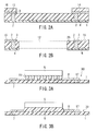
- FIG. 2A is a sectional view of an upper or inner conductive-via provided insulating substrate in a step of a method of manufacturing the semiconductor device according to the first embodiment of the present invention
- FIG. 2B is a sectional view of the inner conductive-via provided insulating substrate in a step of the method of manufacturing the semiconductor device according to the first embodiment of the present invention
- FIG. 3A is a sectional view of a wiring printed substrate in a step of the method of manufacturing the semiconductor device according to the first embodiment of the present invention
- FIG. 3B is a sectional view of the wiring printed substrate in a step of the method of manufacturing the semiconductor device according to the first embodiment of the present invention
- FIG. 4 is a sectional view of the inner conductive-via provided insulating substrate and the wiring printed substrate in a superposing step of the method of manufacturing the semiconductor device according to the first embodiment of the present invention
- FIG. 5 is a sectional view of the semiconductor device manufactured by the manufacturing method according to the first embodiment of the present invention.
- FIG. 6 is a sectional view of a semiconductor device manufactured by a manufacturing method according to a second embodiment of the present invention.
- FIG. 7A is a sectional view of an upper, outer conductive-via provided insulating substrate in a step of a method of manufacturing a semiconductor device according to a third embodiment of the present invention.
- FIG. 7B is a sectional view of an inner conductive-via provided insulating substrate in a step of the method of manufacturing the semiconductor device according to the third embodiment of the present invention.
- FIG. 7C is a sectional view of a wiring printed substrate in a step of the method of manufacturing the semiconductor device according to the third embodiment of the present invention.
- FIG. 7D is a sectional view of a superposed structure in a step of the method of manufacturing the semiconductor device according to the third embodiment of the present invention.
- FIG. 7E is a sectional view of the superposed structure in a step of the method of manufacturing the semiconductor device according to the third embodiment of the present invention.
- FIG. 7F is a sectional view of the semiconductor device manufactured by the manufacturing method according to the third embodiment of the present invention.
- FIG. 8 is a sectional view of a semiconductor device manufactured by a manufacturing method according to a fourth embodiment of the present invention.
- FIG. 9A is a sectional view of a semiconductor device manufactured by a manufacturing method according to a fifth embodiment of the present invention.
- FIG. 9B is a sectional view of a detailed structure of a semiconductor element portion of a semiconductor device shown in FIG. 9 A.
- FIGS. 1A, 1 B, 4 , and 5 the semiconductor device of the first embodiment of the present invention will be described with reference to FIGS. 1A, 1 B, 4 , and 5 .
- FIG. 1A is an exploded perspective view of the semiconductor device according to a first embodiment of the present invention.
- FIG. 1B is a perspective view of a lower, outer conductive-via provided insulating substrate of the semiconductor device of FIG. 1A, in which the insulating substrate is upside down to show the lower surface of the insulating substrate, and shows, in particular, external terminals of the lower insulating substrate in the practical shape.
- FIG. 4 is a sectional view of the inner conductive-via provided insulating substrate and the wiring printed substrate in a superposing step of the method of manufacturing the semiconductor device according to the first embodiment of the present invention.
- FIG. 5 is a sectional view of the semiconductor device manufactured by the manufacturing method according to the first embodiment of the present invention.
- the superposed type package is comprised of a conductive-via provided insulating substrate 20 having an opening 12 in the center thereof for accommodating a semiconductor element 5 , a wiring printed substrate 30 which carries the semiconductor element 5 , an upper, outer conductive-via provided insulating substrate 20 a constituting an upper cover plate, and a lower, outer conductive-via provided insulating substrate 20 b constituting a lower cover plate and having external terminals 10 .
- An insulating substrate 1 in which copper foil is formed on the surface thereof as a conductive film for example, a polyimide substrate in which a copper foil of about 40 ⁇ m in thickness is formed on the surface is utilized as the wiring printed substrate 30 for carrying the semiconductor element.
- the conductive film is not restricted to copper foil, and any conductive material film suitable for the wiring conductor layer can be used.
- the thickness of the conductive film of about 40 ⁇ m is just an ordinary value and therefore the thickness is not restricted to this value.
- As the wiring printed substrate 30 it is permissible to use an insulating substrate comprised of multiple layers of the polyimide substrates each in which the conductive film is formed on the surface thereof.
- Via holes are provided in the insulating substrate 6 and a contact electrode 7 is buried in each via hole.
- the copper foil on the insulating substrate 1 is patterned and lands 17 are formed on the contact electrodes 7 by the patterned copper foil.
- Wirings 8 electrically connected to the conductor element 5 are formed by the patterned copper foil.
- the thickness (substantially, the thickness of a silicon chip) of the semiconductor element 5 is about 30 to 200 ⁇ m, preferably about 50 to 150 ⁇ m (FIG. 4 ).
- the insulating substrate 6 in which a conductive film of copper foil is formed on the surface thereof is utilized, like the polyimide substrate in which copper foil of about 75 ⁇ m in thickness is formed on the surface thereof.
- the conductive film is not restricted to copper foil, and any conductive material film suitable for a wiring conductor layer may be used.
- the thickness of the conductive film of about 75 ⁇ m is just an ordinary value and therefore the thickness is not restricted to this value.
- Via holes are provided in the insulating substrate 6 and a contact electrode 2 is buried in each via hole.
- the copper foil on the insulating substrate 6 is patterned and the lands 3 are formed on the contact electrodes 2 with the patterned copper foil. Further, the wiring conductors 16 are formed by the patterned copper foil.
- An opening (chip cavity) 12 for accommodating the semiconductor element 5 is formed in the center of the insulating substrate 6 .
- the size of the cavity 12 is larger than that of the semiconductor element 5 to accommodate the semiconductor element 5 in the cavity 12 .
- a thermosetting adhesive agent 4 such as epoxy resin is applied to the lower surface of the conductive-via provided insulating substrate 20 (FIG. 4 ). Such adhesive agent 4 may be applied to both of the lower and upper surfaces of the insulating substrate 6 .
- the conductive-via provided insulating substrate 20 and the wiring printed substrate 30 are superposed and integrated to each other by adhesive agent 4 charged in the chip cavity 12 to form a superposed substrate (FIG. 4 ). That is, the conductive-via provided insulating substrate 20 and the wiring printed substrate 30 are pressured in opposing directions while being heated to integrate the substrates 20 and the substrate 30 . When the conductive-via provided insulating substrate 20 and the wiring printed substrate 30 are pressured in opposing directions while being heated, then the substrates 20 and the substrate 30 are integrated to each other by adhesive agent 4 which is coated on the lower surface of the conductive-via provided insulating substrate 20 .
- a flexible material of an flexible adhesive film 15 made of, for example silicone resin, provided on the surface of the semiconductor element is charged into a space between the semiconductor element and the inner wall of the chip cavity 12 .
- Via holes are provided in the upper conductive-via provided insulating substrate 20 a, and the contact electrode 2 is buried in each via hole (FIG. 5 ).
- the land 3 is formed on each contact electrode 2 .
- the upper conductive-via provided insulating substrate 20 a is provided with a wiring conductor, if it is necessary.
- the lower conductive-via provided insulating substrate 20 b also includes via holes and the contact electrode 2 is buried in the via hole (FIG. 5 ).
- the lower conductive-via provided insulating substrate 20 b contains the wiring conductors 16 and lands 3 and the external terminals 10 are formed on the rear face thereof (FIGS. 1 A and 1 B).
- One surface of the lower conductive-via provided insulating substrate 20 b is in contact with the lower surface of the wiring printed substrate 30 of the lowermost superposed substrate so that the contact electrodes 2 the lower conductive-via provided insulating substrate 20 b are electrically connected to the contact electrodes 7 of the lower surface of the wiring printed substrate 30 of the lowermost superposed substrate.
- the external terminals 10 are formed on the other surface of the conductive-via provided insulating substrate 20 b, and electrically connected to the contact electrodes 2 of lower conductive-via provided insulating substrate 20 b. In FIG. 5, the external terminals 10 are omitted for simplicity.
- the semiconductor device comprised of thin superposed type package can be obtained.
- the superposed structure comprising a plurality of superposed substrates (in this embodiment, four superposed substrates) each composed of the conductive-via provided insulating substrate 20 and the wiring printed substrate 30 is sandwiched between the upper and lower conductive-via provided insulating substrates, airproof of the semiconductor elements is secured.
- the semiconductor element is accommodated in the chip cavity formed in the conductive-via provided insulating substrate of each superposed substrate. Since the chip cavity is smaller than the semiconductor element, when the semiconductor element is accommodated in the chip cavity, there is formed a space between the semiconductor element and an inner wall of the chip cavity.
- a flexible adhesive agent such as elastomer, for example silicone resin, is filled in this space.
- elastomer for example silicone resin
- airproof is increased so that moisture resistance of the semiconductor element is improved.
- the adhesive agent is flexible, then stress can be absorbed. Therefore, even if the semiconductor device is a little bent and thus the semiconductor element is elongated, the flexible adhesive agent absorbs the elongation of the semiconductor element. That is, even if an external force is applied to the semiconductor device, a generated stress can be absorbed by the flexible adhesive agent.
- the flexible adhesive agent need not necessarily be provided, and the space may leave as it is. Even the space can absorb the elongation of the semiconductor element.
- FIGS. 2A, 2 B, 3 A, 3 B, 4 and 5 A second embodiment of the present invention will be described with reference to FIGS. 2A, 2 B, 3 A, 3 B, 4 and 5 .
- FIG. 2A is a sectional view of an upper or inner conductive-via provided insulating substrate in a step of a method of manufacturing the semiconductor device shown in FIGS. 1 and 5.
- FIG. 2B is a sectional view of the inner conductive-via provided insulating substrate in a step of the method of manufacturing the semiconductor device shown in FIGS. 1 and 5.
- FIG. 3A is a sectional view of a wiring printed substrate in a step of the method of manufacturing the semiconductor device shown in FIGS. 1 and 5.
- FIG. 3B is a sectional view of the wiring printed substrate in a step of the method of manufacturing the semiconductor device shown in FIGS. 1 and 5.
- FIG. 4 is a sectional view of the inner conductive-via provided insulating substrate and the wiring printed substrate in a superposing step of the method of manufacturing the semiconductor device according to the first embodiment of the present invention.
- FIG. 5 is a sectional view of the semiconductor device manufactured by the manufacturing method according to the first embodiment of the present invention.
- the insulating substrate 6 in which a conductive film of copper foil is formed on the surface thereof is utilized, like the polyimide substrate in which copper foil of about 75 ⁇ m in thickness is formed on the surface thereof.
- the conductive film is not restricted to copper foil, and any conductive material film suitable for a wiring conductor layer may be used.
- the thickness of the conductive film of about 75 ⁇ m is just an ordinary value and therefore the thickness is not restricted to this value.
- via holes 13 are formed at portions of the insulating substrate 6 in which the contact electrodes 2 are to be buried using YAG laser, carbon dioxide gas laser or the like. Then, after resist films 14 are formed on regions corresponding to the via and the wiring conductor, the copper foil formed on the insulating substrate 6 is etched, using the resist films 14 as masks, so as to form the land 3 and the wiring conductor patterns 16 . Thereafter, the masks 14 are removed. After that, silver filler or copper filler contained conductive resin paste is screen-printed into the via holes 13 from the lower surface of the insulating substrate 6 so as to form the contact electrodes 2 in the via holes 13 .
- thermosetting adhesive agent 4 such as epoxy resin is applied to the lower face of the insulating substrate 6 .
- an upper, outer conductive-via provided insulating substrate 20 a is formed (FIG. 2 A).
- the substrate shown in FIG. 2A is further processed so that a region in which the semiconductor element is to be accommodated of the insulating substrate 6 is punched out (FIG. 2 B). The punched-out region is used as the chip cavity 12 .
- An insulating substrate 1 in which copper foil is formed on the surface thereof as a conductive film for example, a polyimide substrate in which a copper foil of about 40 ⁇ m in thickness is formed on the surface is utilized as the wiring printed substrate 30 for carrying the semiconductor element.
- the conductive film is not restricted to copper foil, and any conductive material film suitable for the wiring conductor layer can be used.
- the thickness of the conductive film of about 40 ⁇ m is just an ordinary value and therefore the thickness is not restricted to this value.
- As the wiring printed substrate 30 it is permissible to use an insulating substrate comprised of multiple layers of the polyimide substrates each in which the conductive film is formed on the surface thereof.
- Via holes are formed at portions of the insulating substrate 1 of the wiring printed substrate 30 in which the contact electrodes 7 are to be buried using YAG laser, carbon dioxide laser or the like. Then, after masks (not shown) are formed at regions corresponding to the via holes and the wiring conductors of the insulating substrate 1 , the copper foil is etched so as to form the lands 17 and the wiring conductor patterns 8 . After that, silver filler or copper filler contained conductive resin paste is screen-printed in the via holes so as to form the contact electrodes 7 in the via holes 13 . As the method for forming the contact electrodes 7 , it is permissible to plate an inner walls of the via holes with copper or gold and then fill the via holes with conductive material.
- the semiconductor element (semiconductor chip) 5 is loaded on the wiring printed substrate 30 by die bonding.
- the contact electrodes 11 such as soldering ball are connected to the wiring conductor patterns 8 (FIG. 3 A).
- the semiconductor element 5 is electrically connected to the contact electrodes 7 of the wiring printed substrate 30 through the wiring conductor patterns 8 .
- the contact electrodes 11 are covered with and protected by a flexible adhesive agent 9 such as silicone resin (FIG. 3 B).
- a film 15 made of a flexible adhesive agent such as silicone resin is formed on the surface of the semiconductor element 5 (FIG. 3 C).
- the film 15 and the adhesive agent 9 may be the same material, for example, silicone resin.
- the film 15 is not shown in FIGS. 3A and 3B for simplicity.
- the conductive-via provided insulating substrate 20 is positioned and superposed on the wiring printed substrate 30 to form a superposed substrate.
- the conductive-via provided insulating substrate 20 and the wiring printed substrate 30 are positioned such that the semiconductor element 5 loaded on the wiring printed substrate 30 is disposed in the chip cavity 12 of the conductive-via provided insulating substrate 20 (FIG. 4) and the contact electrodes 2 of the conductive-via provided insulating substrate 20 are electrically connected to the contact electrodes 7 of the wiring printed substrate 30 .
- the superposed structure includes four such superposed substrates.
- the upper conductive-via provided insulating substrate 20 a and the lower conductive-via provided insulating substrate 20 b are provided on the upper surface and the lower surface of the superposed structure, respectively.
- the superposed structure is pressed with a heating press machine such as a vacuum press at a hardening temperature of the adhesive agent 4 to provide the semiconductor device of a superposed type package (FIG. 5 ).
- FIG. 6 is a sectional view of a semiconductor device manufactured by a manufacturing method according to the second embodiment of the present invention.
- a plurality of chip cavities 12 are formed in the conductive-via provided insulating substrate 20 , and a plurality of semiconductor elements 5 are loaded on the wiring printed substrate 30 .
- This embodiment is substantially the same as the first embodiment except for this feature.
- the semiconductor device of this embodiment comprises a plurality of the conductive-via provided insulating substrates 20 each having a plurality of chip cavities 12 (in this embodiment, two chip cavities) and a plurality of the wiring printed substrates 30 (in this embodiment, four wiring printed substrates) each having a plurality of semiconductor elements 5 (in this embodiment, two semiconductor elements).
- the conductive-via provided insulating substrate 20 and the wiring printed substrate 30 are alternately superposed to form a superposed structure.
- the superposed structure is cut out along an outer shape of each package, i.e., along a semiconductor element region as a unit to form individual superposed packages, thereby increasing the effectiveness in manufacturing the semiconductor device with the superposed type package.
- FIG. 6 the corresponding portions or parts to those in FIG. 5 are denoted by the same reference numerals.
- the semiconductor device of this embodiment comprises a plurality of the conductive-via provided insulating substrates 20 each having a plurality of chip cavities 12 (in this embodiment, two chip cavities) and a plurality of the wiring printed substrates 30 (in this embodiment, four wiring printed substrates) each having a plurality of semiconductor elements 5 (in this embodiment, two semiconductor elements).
- the conductive-via provided insulating substrate 20 and the wiring printed substrate 30 are alternately superposed to form a superposed structure.
- the upper conductive-via provided insulating substrate 40 a and the lower conductive-via provided insulating substrate 40 b are provided on the upper surface and the lower surface of the superposed structure, respectively.
- the semiconductor device shown in FIG. 6 comprises four inner conductive-via provided insulating substrates 20 each having two chip cavities 12 and four wiring printed substrates 30 each having four semiconductor elements 5 , an upper, outer conductive-via provided insulating substrate 20 a constituting an upper cover plate, and a lower, outer conductive-via provided insulating substrate 20 b constituting a lower cover plate. That is, in the superposed type package, superposed substrates each including the conductive-via provided insulating substrates 20 and the wiring printed substrates 30 superposed to each other are superposed between the upper layer conductive-via provided insulating substrate 20 a and the lower conductive-via provided insulating substrate 20 b. The superposed layers are heated with pressure so that they are integrated together. The superposed structure is cut out along an outer shape of each package, i.e., along a semiconductor element region as a unit to form individual superposed packages.
- a plurality of the conductive-via provided insulating substrates 20 each having a plurality of chip cavities 12 and a plurality of the wiring printed substrates 30 each having a plurality of semiconductor elements 5 are alternately superposed to form a superposed structure, and the superposed structure is cut out along a semiconductor element region as a unit to form individual superposed packages.
- the same advantages as those provided in the first embodiment can be obtained. That is, since the superposed structure comprising a plurality of superposed substrates each composed of the conductive-via provided insulating substrate 20 and the wiring printed substrate 30 is sandwiched between the upper and lower conductive-via provided insulating substrates, airproof to the semiconductor elements is secured. Further, the semiconductor element is accommodated in the chip cavity formed in the conductive-via provided insulating substrate of each superposed substrate. Since the chip cavity is smaller than the semiconductor element, when the semiconductor element is accommodated in the chip cavity, there is formed a space between the semiconductor element and an inner wall of the chip cavity. A flexible adhesive agent such as elastomer, for example silicone resin, is filled in this space.
- elastomer for example silicone resin
- the adhesive agent By filling such an adhesive agent, airproof is increased so that moisture resistance of the semiconductor element is improved. Furthermore, since the adhesive agent is flexible, then stress can be absorbed. Therefore, even if the semiconductor device is a little bent and thus the semiconductor element is elongated, the flexible adhesive agent absorbs the elongation of the semiconductor element. That is, even if an external force is applied to the semiconductor device, a generated stress can be absorbed by the flexible adhesive agent.
- the flexible adhesive agent need not necessarily be provided, and the space may leave as it is. Even the space can absorb the elongation of the semiconductor element.
- FIGS. 7A to 7 F A third embodiment of the present invention will be described with reference to FIGS. 7A to 7 F.
- FIG. 7A is a sectional view of an upper, outer conductive-via provided insulating substrate 40 a in a step of a method of manufacturing a semiconductor device according to a third embodiment of the present invention.
- FIG. 7B is a sectional view of an inner conductive-via provided insulating substrate 40 in a step of the method of manufacturing the semiconductor device according to the third embodiment of the present invention.
- FIG. 7C is a sectional view of a wiring printed substrate 50 in a step of the method of manufacturing the semiconductor device according to the third embodiment of the present invention.
- FIG. 7D is a sectional view of a superposed structure in a step of the method of manufacturing the semiconductor device according to the third embodiment of the present invention.
- FIG. 7A is a sectional view of an upper, outer conductive-via provided insulating substrate 40 a in a step of a method of manufacturing a semiconductor device according to a third embodiment of the present invention.
- FIG. 7B is a sectional view of an inner conductive-via provided
- FIG. 7E is a sectional view of the superposed structure in a step of the method of manufacturing the semiconductor device according to the third embodiment of the present invention.
- FIG. 7F is a sectional view of the semiconductor device manufactured by the manufacturing method according to the third embodiment of the present invention.
- a plurality of chip cavities 32 are formed in the conductive-via provided insulating substrate 40 , and a plurality of semiconductor elements 25 are loaded on the wiring printed substrate 50 .
- the semiconductor device of this embodiment comprises a plurality of the conductive-via provided insulating substrates 40 each having a plurality of chip cavities 32 (in this embodiment, two chip cavities) and a plurality of the wiring printed substrates 50 (in this embodiment, four wiring printed substrates) each having a plurality of semiconductor elements 25 (in this embodiment, two semiconductor elements).
- the conductive-via provided insulating substrate 40 and the wiring printed substrate 50 are alternately superposed to form a superposed structure.
- the upper conductive-via provided insulating substrate 40 a and the lower conductive-via provided insulating substrate 40 b are provided on the upper surface and the lower surface of the superposed structure, respectively.
- the insulating substrate 26 in which conductive film of copper foil is formed on the surface thereof is utilized, like the polyimide substrate in which copper foil is formed on the surface thereof as conductive film.
- the conductive film is not restricted to copper foil and any conductive material film suitable for the wiring conductor layer may be used.
- the conductive-via provided insulating substrate 40 a and 40 b and the conductive-via provided insulating substrate 40 it is permissible to use such a superposed substrate comprised of plural superposed polyimide substrates each in which conductive film of copper foil is formed on the surface thereof.
- the outer, upper conductive-via provided insulating substrate 40 a masks (not shown) are formed on region corresponding to the via holes and the wiring conductors of the insulating substrate 26 . Then, the copper foil is etched so as to form the lands 23 and the wiring conductor patterns. Thermosetting adhesive agent 24 such as epoxy resin is applied to the lower surface of the insulating substrate 26 (FIG. 7 A). Similarly, in forming the inner conductive-via provided insulating substrate 40 , masks (not shown) are formed on region corresponding to the via holes and the wiring conductors of the insulating substrate 26 . Thermosetting adhesive agent 24 such as epoxy resin is applied to the lower surface of the insulating substrate 26 .
- a region of the insulating substrate 26 in which the semiconductor element is to be accommodated is punched out so that it is used as the chip cavity 32 (FIG. 7 B).
- the chip cavity 32 (FIG. 7 B).
- two chip cavities are provided. It is preferable to provide two or more chip cavities to more improve effectiveness in manufacturing process.
- the insulating substrate 21 in which copper foil conductive film is formed on the surface thereof is utilized, like the polyimide substrate in which the copper foil conductive film is formed on the surface thereof.
- the conductive film is not restricted to the copper foil, however any conductive material film suitable for the wiring conductor layer may be used.
- the wiring printed substrate 30 it is permissible to use the printed superposed plate comprised of multiple superposed polyimide substrates each in which conductive film of copper foil is formed on the surface thereof.
- Masks are formed on regions of the insulating substrate 21 corresponding to the via holes and the wiring conductors and after that, the copper foil is etched so as to form the lands 37 and the wiring conductor patterns 28 FIG.
- the surface of the semiconductor element 25 in which the contact electrodes (not shown) are provided is covered with and protected by a flexible adhesive agent 29 such as silicone resin (FIG. 3 B). Furthermore, a film 30 made of a flexible adhesive agent such as silicone resin is formed on the opposite surface of the semiconductor element 25 .
- the film 30 and the adhesive agent 29 may be the same material, for example, silicone resin.
- the semiconductor element 25 (semiconductor chip) is loaded on the wiring printed substrate 50 by means of, for example, the flip chip method. According to this embodiment, two semiconductor elements 25 are loaded on the wiring printed substrate 50 (FIG. 7 C).
- the conductive-via provided insulating substrate 40 is positioned and superposed on the wiring printed substrate 50 so that the semiconductor element 25 loaded on the wiring printed substrate 50 is disposed in the chip cavity 32 of the conductive-via provided insulating substrate 40 .
- the superposed structure includes four such superposed substrates each comprising the conductive-via provided insulating substrate 40 and the wiring printed substrate 50 .
- the upper conductive-via provided insulating substrate 40 a and the lower conductive-via provided insulating substrate 40 b are provided on the upper surface and the lower surface of the superposed structure, respectively.
- the superposed structure is pressed with a heating press machine such as a vacuum press at a hardening temperature of the adhesive agent 24 to provide the semiconductor device of a superposed type package (FIG. 7 D).
- the above superposed structure having the contact electrodes 31 is cut out along an outer shape of each package, i.e., with a region including one semiconductor element as a unit, by means of a blade, router or the like so as to form individual superposed packages (FIG. 7 E).
- a plurality of chip cavities 32 are formed in the conductive-via provided insulating substrate 40 , and a plurality of semiconductor elements 25 are loaded on the wiring printed substrate 50 . Then, by superposing the substrates 40 and 50 alternately, an superposed structure is formed and finally, the superposed structure is cut to multiple packages by means of a blade. Consequently, effectiveness of formation of the superposed package is achieved.
- this superposed structure is sandwiched between the upper conductive-via provided insulating substrate 40 a in which the chip cavity is not formed and the lower conductive-via provided insulating substrate 40 b in which the chip cavity is not formed.
- the semiconductor elements 25 are sealed tightly so that the reliability of the package structure is improved.
- External terminals (not shown) of an appropriate shape are formed on the lower conductive-via provided insulating substrate 40 b.
- the wiring printed substrates 50 loaded with the semiconductor element 25 and the conductive-via provided insulating substrate 40 are superposed and finally, by cutting the superposed structure, the superposed packages can be produced with fewer processes than the conventional manufacturing method for the package.
- FIG. 8 is a sectional view of a semiconductor device manufactured by a manufacturing method according to a fourth embodiment of the present invention.
- This semiconductor device is comprised of a plurality of wiring printed substrates 50 each having the semiconductor element 25 mounted thereon and a plurality of conductive-via provided insulating substrates 40 each having the chip cavity 32 which is a space for accommodating the semiconductor element 25 loaded on the wiring printed substrate 50 .
- the conductive-via provided insulating substrates 40 and the wiring printed substrates 50 are alternately superposed so as to provide the superposed structure for the semiconductor elements.
- four pieces of semiconductor elements 25 are superposed to provide the superposed structure.
- This superposed structure is sandwiched between the upper conductive-via provided insulating substrate 40 a in which the chip cavity is not formed and the lower conductive-via provided insulating substrate 40 b in which the chip cavity is not formed, so that the semiconductor elements 25 are sealed completely thereby improving the reliability of the package structure.
- the contact electrode connected to each semiconductor element 25 through the wiring conductor is formed inside the via hole.
- the contact electrode is comprised of a contact electrode 31 a connected to a ground (GND) wire line, and contact electrodes 31 b, 31 c connected to a signal wire line.
- metallic film 33 composed of aluminum, copper or the like is formed on the upper and lower conductive-via provided insulating substrates 40 a, 40 b.
- the metallic film 33 is formed of, for example, metallic foil.
- the metallic film 33 is formed of a metallic layer obtained by spattering aluminum or copper.
- This metallic film 33 is electrically connected to the contact electrode 31 a connected to the ground wire line and not connected to the contact electrodes 31 b, 31 c connected to the signal wire line.
- FIGS. 9A and 9B a fifth embodiment of the present invention will be described with reference to FIGS. 9A and 9B.
- FIG. 9A is a sectional view of a semiconductor device manufactured by a manufacturing method according to a fifth embodiment of the present invention
- FIG. 9B is a sectional view of a detailed structure of a semiconductor element portion of a semiconductor device shown in FIG. 9 A.
- the semiconductor device of this embodiment is comprised of a plurality of wiring printed substrates 50 each having the semiconductor element 25 mounted thereon and a plurality of conductive-via provided insulating substrates 40 including the chip cavity 32 which is a space for accommodating the semiconductor element 25 loaded on the wiring printed substrate 50 so as to realize the superposed structure for the semiconductor elements (FIG. 9 A).
- the superposed structure of this embodiment four pieces of the semiconductor elements 25 are superposed. This superposed structure is sandwiched between the upper conductive-via provided insulating substrate 40 a in which the chip cavity is not formed and the lower conductive-via provided insulating substrate 40 b in which the chip cavity is not formed. Consequently, the semiconductor elements 25 are tightly sealed thereby improving the reliability of the package structure.
- the semiconductor element 25 is comprised of silicon chips 25 a, 25 b, 25 c, 25 d and the silicon chips 25 a, 25 b, 25 c, 25 d are superposed successively through a bump 34 which is a contact electrode (FIG. 9 B).
- the superposed structure can be formed in more layers than the semiconductor device of the first to fourth embodiments and the superposed package can be formed thinner.
- the semiconductor device comprised of such thinner superposed packages can be obtained. Further, this superposed structure is sandwiched between the upper conductive-via provided insulating substrate in which the chip cavity is not formed and the lower conductive-via provided insulating substrate in which the chip cavity is not formed. Consequently, the semiconductor elements are sealed completely thereby improving the reliability of the package structure.
- the semiconductor element is accommodated in the chip cavity formed in the conductive-via provided insulating substrate of each superposed substrate. Because the size of the chip cavity is smaller than that of the semiconductor element, when the semiconductor element is accommodated in the chip cavity, there is formed a space between the semiconductor element and an inner wall of the chip cavity.
- a flexible adhesive agent such as elastomer, for example silicone resin, is filled in this space.
- elastomer for example silicone resin
- the flexible adhesive agent absorbs the elongation of the semiconductor element. That is, even if an external force is applied to the semiconductor device, a generated stress can be absorbed by the flexible adhesive agent.
- the flexible adhesive agent need not necessarily be provided, and the space may leave as it is. Even the space can absorb the elongation of the semiconductor element. Further, by superposing plurality of the wiring printed substrates each containing the semiconductor element and the conductive-via provided insulating substrates and cutting that superposed structure, the superposed packages can be manufactured with fewer manufacturing processes than a conventional manufacturing process.
Abstract
Description
Claims (14)
Applications Claiming Priority (2)
| Application Number | Priority Date | Filing Date | Title |
|---|---|---|---|
| JP11-239033 | 1999-08-26 | ||
| JP1999239033A JP3934284B6 (en) | 1999-08-26 | Semiconductor device and manufacturing method of semiconductor device |
Publications (1)
| Publication Number | Publication Date |
|---|---|
| US6469374B1 true US6469374B1 (en) | 2002-10-22 |
Family
ID=17038891
Family Applications (1)
| Application Number | Title | Priority Date | Filing Date |
|---|---|---|---|
| US09/648,373 Expired - Lifetime US6469374B1 (en) | 1999-08-26 | 2000-08-25 | Superposed printed substrates and insulating substrates having semiconductor elements inside |
Country Status (3)
| Country | Link |
|---|---|
| US (1) | US6469374B1 (en) |
| KR (1) | KR100375118B1 (en) |
| TW (1) | TW472330B (en) |
Cited By (43)
| Publication number | Priority date | Publication date | Assignee | Title |
|---|---|---|---|---|
| US20010008794A1 (en) * | 2000-01-13 | 2001-07-19 | Masatoshi Akagawa | Semiconductor device and manufacturing method therefor |
| US20010054756A1 (en) * | 2000-06-21 | 2001-12-27 | Michio Horiuchi | Multi-layered semiconductor device and method for producing the same |
| US20030030143A1 (en) * | 2001-08-10 | 2003-02-13 | Ingo Wennemuth | Electronic component with stacked electronic elements and method for fabricating an electronic component |
| US20030137045A1 (en) * | 2002-01-23 | 2003-07-24 | Matsushita Electric Industrial Co., Ltd. | Circuit component built-in module and method of manufacturing the same |
| US20030159852A1 (en) * | 2002-02-25 | 2003-08-28 | Fujitsu Limited | Multilayer wiring board, manufacturing method therefor and test apparatus thereof |
| US20040004280A1 (en) * | 2002-07-04 | 2004-01-08 | Manabu Shibata | Semiconductor device and system having semiconductor device mounted thereon |
| US6680441B2 (en) | 2001-06-13 | 2004-01-20 | Denso Corporation | Printed wiring board with embedded electric device and method for manufacturing printed wiring board with embedded electric device |
| US6686222B2 (en) * | 2001-05-18 | 2004-02-03 | Kabushiki Kaisha Toshiba | Stacked semiconductor device manufacturing method |
| US20040080045A1 (en) * | 2002-10-28 | 2004-04-29 | Sharp Kabushiki Kaisha | Semiconductor device and chip-stack semiconductor device |
| US6768186B2 (en) | 2002-10-15 | 2004-07-27 | Semiconductor Components Industries, L.L.C. | Semiconductor device and laminated leadframe package |
| US20040157410A1 (en) * | 2003-01-16 | 2004-08-12 | Seiko Epson Corporation | Semiconductor device, semiconductor module, electronic equipment, method for manufacturing semiconductor device, and method for manufacturing semiconductor module |
| US20040183192A1 (en) * | 2003-01-31 | 2004-09-23 | Masashi Otsuka | Semiconductor device assembled into a chip size package |
| US20040188855A1 (en) * | 2002-04-19 | 2004-09-30 | Fujitsu Limited | Semiconductor device and manufacturing methods thereof |
| US20040238935A1 (en) * | 2001-09-28 | 2004-12-02 | Atsushi Yoshimura | Semiconductor device and method of manufacturing semiconductor device |
| EP1489657A1 (en) * | 2002-02-06 | 2004-12-22 | Ibiden Co., Ltd. | Semiconductor chip mounting board, its manufacturing method, and semiconductor module |
| WO2005006438A1 (en) | 2003-06-30 | 2005-01-20 | Intel Corporation | Microelectronic package method and apparatus |
| US20050253247A1 (en) * | 2004-04-30 | 2005-11-17 | Takashi Imoto | Semiconductor device and manufacturing method therefor |
| EP1601017A1 (en) * | 2003-02-26 | 2005-11-30 | Ibiden Co., Ltd. | Multilayer printed wiring board |
| US20060049995A1 (en) * | 2004-09-01 | 2006-03-09 | Toshikazu Imaoka | Integrated antenna type circuit apparatus |
| US20060079020A1 (en) * | 2004-10-13 | 2006-04-13 | Shoko Omizo | Semiconductor device and a method of assembling a semiconductor device |
| US20060087020A1 (en) * | 2004-10-22 | 2006-04-27 | Matsushita Electric Industrial Co., Ltd. | Semiconductor device and method for producing the same |
| DE102005043557A1 (en) * | 2005-09-12 | 2006-09-28 | Infineon Technologies Ag | Semiconductor device for electronic device, has through contact arranged in prefabricated through contact flat rod, which is positioned in end region of device and exhibits through opening which is filled with metal |
| EP1724832A2 (en) * | 2005-05-20 | 2006-11-22 | Matsushita Electric Industrial Co., Ltd. | Multilayer module formed of modules stacked on top of each other and method of manufacturing the same |
| US20070018313A1 (en) * | 2005-07-21 | 2007-01-25 | Shinko Electric Industries Co., Ltd. | Electronic parts packaging structure and method of manufacturing the same |
| US20070120248A1 (en) * | 2005-11-25 | 2007-05-31 | Atsushi Yoshimura | Semiconductor device |
| US20070158806A1 (en) * | 2006-01-12 | 2007-07-12 | Stats Chippac Ltd. | Integrated circuit package system including honeycomb molding |
| US20070210429A1 (en) * | 2006-03-07 | 2007-09-13 | Industrial Technology Research Institute | Package structure for electronic device |
| US20070296073A1 (en) * | 2006-06-27 | 2007-12-27 | Taiwan Semiconductor Manufacturing Co., Ltd. | Three dimensional integrated circuit and method of making the same |
| US20080099903A1 (en) * | 2006-10-31 | 2008-05-01 | Industrial Technology Research Institute | Stacked chip package, embedded chip package and fabricating method thereof |
| US20080142943A1 (en) * | 2006-12-18 | 2008-06-19 | Hyun Joung Kim | Integrated circuit package system with thermo-mechanical interlocking substrates |
| US20080224298A1 (en) * | 2007-03-12 | 2008-09-18 | Micron Technology, Inc. | Apparatus for packaging semiconductor devices, packaged semiconductor components, methods of manufacturing apparatus for packaging semiconductor devices, and methods of manufacturing semiconductor components |
| US20080304242A1 (en) * | 2007-06-07 | 2008-12-11 | Samsung Electronics Co., Ltd. | Stack module, card including the stack module, and system including the stack module |
| US20090020885A1 (en) * | 2006-12-28 | 2009-01-22 | Masanori Onodera | Semiconductor device and method of manufacturing the same |
| US20090250801A1 (en) * | 2008-04-03 | 2009-10-08 | Elpida Memory, Inc. | Semiconductor device |
| US20100052187A1 (en) * | 2008-09-01 | 2010-03-04 | Woong Sun Lee | Stacked semiconductor package and method for fabricating the same |
| US20100148339A1 (en) * | 2008-12-11 | 2010-06-17 | Stmicroelectronics (Grenoble) Sas | Process for fabricating a semiconductor component support, support and semiconductor device |
| US20100246141A1 (en) * | 2009-03-31 | 2010-09-30 | Hong Kong Applied Science and Technology Research Institute Co. Ltd. (ASTRI) | Electronic package and method of fabrication thereof |
| WO2010111825A1 (en) * | 2009-03-30 | 2010-10-07 | Hong Kong Applied Science And Technology Research Institute Co., Ltd. | Electronic package and method of fabrication thereof |
| US20100279504A1 (en) * | 2006-01-12 | 2010-11-04 | Heap Hoe Kuan | Integrated circuit package system including honeycomb molding |
| US20120262974A1 (en) * | 2003-04-21 | 2012-10-18 | Elpida Memory, Inc. | Memory module and memory system |
| US20120313245A1 (en) * | 2011-06-13 | 2012-12-13 | Shinko Electric Industries Co., Ltd. | Semiconductor device |
| US8860202B2 (en) * | 2012-08-29 | 2014-10-14 | Macronix International Co., Ltd. | Chip stack structure and manufacturing method thereof |
| US20150221570A1 (en) * | 2014-02-04 | 2015-08-06 | Amkor Technology, Inc. | Thin sandwich embedded package |
Families Citing this family (2)
| Publication number | Priority date | Publication date | Assignee | Title |
|---|---|---|---|---|
| KR100621437B1 (en) * | 2004-11-15 | 2006-09-08 | 삼성전자주식회사 | Mounting structure of easily reparable semiconductor package, stack package and semiconductor module |
| KR100833589B1 (en) | 2006-03-29 | 2008-05-30 | 주식회사 하이닉스반도체 | Stack package |
Citations (11)
| Publication number | Priority date | Publication date | Assignee | Title |
|---|---|---|---|---|
| JPH05291318A (en) | 1992-04-07 | 1993-11-05 | Toshiba Corp | Resin sealing-type semiconductor device |
| JPH08236694A (en) | 1995-02-24 | 1996-09-13 | Nec Corp | Semiconductor package and manufacture thereof |
| JPH09219490A (en) | 1995-11-28 | 1997-08-19 | Samsung Electron Co Ltd | Three-dimensional laminated package element |
| JPH10135267A (en) | 1996-10-30 | 1998-05-22 | Oki Electric Ind Co Ltd | Structure of mounting board and its manufacture |
| JPH10163414A (en) | 1996-09-17 | 1998-06-19 | Hitachi Ltd | Multi chip semiconductor device |
| JPH11145381A (en) | 1997-11-12 | 1999-05-28 | Denso Corp | Semiconductor multi-chip module |
| US6180881B1 (en) * | 1998-05-05 | 2001-01-30 | Harlan Ruben Isaak | Chip stack and method of making same |
| US6239496B1 (en) * | 1999-01-18 | 2001-05-29 | Kabushiki Kaisha Toshiba | Package having very thin semiconductor chip, multichip module assembled by the package, and method for manufacturing the same |
| US6239495B1 (en) * | 1998-07-29 | 2001-05-29 | Kabushiki Kaisha Toshiba | Multichip semiconductor device and memory card |
| US6274929B1 (en) * | 1998-09-01 | 2001-08-14 | Texas Instruments Incorporated | Stacked double sided integrated circuit package |
| US20010054758A1 (en) * | 2000-06-21 | 2001-12-27 | Isaak Harlan R. | Three-dimensional memory stacking using anisotropic epoxy interconnections |
-
2000
- 2000-08-18 TW TW089116706A patent/TW472330B/en not_active IP Right Cessation
- 2000-08-25 US US09/648,373 patent/US6469374B1/en not_active Expired - Lifetime
- 2000-08-25 KR KR10-2000-0049496A patent/KR100375118B1/en active IP Right Grant
Patent Citations (13)
| Publication number | Priority date | Publication date | Assignee | Title |
|---|---|---|---|---|
| JPH05291318A (en) | 1992-04-07 | 1993-11-05 | Toshiba Corp | Resin sealing-type semiconductor device |
| US6188127B1 (en) * | 1995-02-24 | 2001-02-13 | Nec Corporation | Semiconductor packing stack module and method of producing the same |
| JPH08236694A (en) | 1995-02-24 | 1996-09-13 | Nec Corp | Semiconductor package and manufacture thereof |
| JPH09219490A (en) | 1995-11-28 | 1997-08-19 | Samsung Electron Co Ltd | Three-dimensional laminated package element |
| US5744827A (en) | 1995-11-28 | 1998-04-28 | Samsung Electronics Co., Ltd. | Three dimensional stack package device having exposed coupling lead portions and vertical interconnection elements |
| JPH10163414A (en) | 1996-09-17 | 1998-06-19 | Hitachi Ltd | Multi chip semiconductor device |
| JPH10135267A (en) | 1996-10-30 | 1998-05-22 | Oki Electric Ind Co Ltd | Structure of mounting board and its manufacture |
| JPH11145381A (en) | 1997-11-12 | 1999-05-28 | Denso Corp | Semiconductor multi-chip module |
| US6180881B1 (en) * | 1998-05-05 | 2001-01-30 | Harlan Ruben Isaak | Chip stack and method of making same |
| US6239495B1 (en) * | 1998-07-29 | 2001-05-29 | Kabushiki Kaisha Toshiba | Multichip semiconductor device and memory card |
| US6274929B1 (en) * | 1998-09-01 | 2001-08-14 | Texas Instruments Incorporated | Stacked double sided integrated circuit package |
| US6239496B1 (en) * | 1999-01-18 | 2001-05-29 | Kabushiki Kaisha Toshiba | Package having very thin semiconductor chip, multichip module assembled by the package, and method for manufacturing the same |
| US20010054758A1 (en) * | 2000-06-21 | 2001-12-27 | Isaak Harlan R. | Three-dimensional memory stacking using anisotropic epoxy interconnections |
Cited By (98)
| Publication number | Priority date | Publication date | Assignee | Title |
|---|---|---|---|---|
| US7053475B2 (en) * | 2000-01-13 | 2006-05-30 | Shinko Electric Industries Co., Ltd. | Semiconductor device and manufacturing method therefor |
| US20010008794A1 (en) * | 2000-01-13 | 2001-07-19 | Masatoshi Akagawa | Semiconductor device and manufacturing method therefor |
| US20010054756A1 (en) * | 2000-06-21 | 2001-12-27 | Michio Horiuchi | Multi-layered semiconductor device and method for producing the same |
| US6849945B2 (en) * | 2000-06-21 | 2005-02-01 | Shinko Electric Industries Co., Ltd | Multi-layered semiconductor device and method for producing the same |
| US6686222B2 (en) * | 2001-05-18 | 2004-02-03 | Kabushiki Kaisha Toshiba | Stacked semiconductor device manufacturing method |
| SG102054A1 (en) * | 2001-06-13 | 2004-02-27 | Denso Corp | Printed wiring board with embedded electric device and method for manufacturing printed wiring board with embedded electric device |
| US6680441B2 (en) | 2001-06-13 | 2004-01-20 | Denso Corporation | Printed wiring board with embedded electric device and method for manufacturing printed wiring board with embedded electric device |
| US7165321B2 (en) | 2001-06-13 | 2007-01-23 | Denso Corporation | Method for manufacturing printed wiring board with embedded electric device |
| US20040091687A1 (en) * | 2001-06-13 | 2004-05-13 | Koji Kondo | Method for manufacturing printed wiring board with embedded electric device |
| US20030030143A1 (en) * | 2001-08-10 | 2003-02-13 | Ingo Wennemuth | Electronic component with stacked electronic elements and method for fabricating an electronic component |
| US20040238935A1 (en) * | 2001-09-28 | 2004-12-02 | Atsushi Yoshimura | Semiconductor device and method of manufacturing semiconductor device |
| US7141872B2 (en) | 2001-09-28 | 2006-11-28 | Kabushiki Kaisha Toshiba | Semiconductor device and method of manufacturing semiconductor device |
| US20030137045A1 (en) * | 2002-01-23 | 2003-07-24 | Matsushita Electric Industrial Co., Ltd. | Circuit component built-in module and method of manufacturing the same |
| US7018866B2 (en) * | 2002-01-23 | 2006-03-28 | Matsushita Electric Industrial Co., Ltd. | Circuit component built-in module with embedded semiconductor chip and method of manufacturing |
| US20040145044A1 (en) * | 2002-01-23 | 2004-07-29 | Matsushita Electric Industrial Co., Ltd. | Circuit component built-in module with embedded semiconductor chip and method of manufacturing |
| US6784530B2 (en) | 2002-01-23 | 2004-08-31 | Matsushita Electric Industrial Co., Ltd. | Circuit component built-in module with embedded semiconductor chip and method of manufacturing |
| EP1489657A4 (en) * | 2002-02-06 | 2011-06-29 | Ibiden Co Ltd | Semiconductor chip mounting board, its manufacturing method, and semiconductor module |
| EP1489657A1 (en) * | 2002-02-06 | 2004-12-22 | Ibiden Co., Ltd. | Semiconductor chip mounting board, its manufacturing method, and semiconductor module |
| US20030159852A1 (en) * | 2002-02-25 | 2003-08-28 | Fujitsu Limited | Multilayer wiring board, manufacturing method therefor and test apparatus thereof |
| US20050246891A1 (en) * | 2002-02-25 | 2005-11-10 | Fujitsu Limited | Multilayer wiring board, manufacturing method therefor and test apparatus thereof |
| US20040066634A1 (en) * | 2002-02-25 | 2004-04-08 | Fujitsu Limited | Multilayer wiring board, manufacturing method therefor and test apparatus thereof |
| US7284311B2 (en) | 2002-02-25 | 2007-10-23 | Fujitsu Limited | Multilayer wiring board, manufacturing method therefor and test apparatus thereof |
| US7091716B2 (en) | 2002-02-25 | 2006-08-15 | Fujitsu Limited | Multilayer wiring board, manufacturing method therefor and test apparatus thereof |
| US20040188855A1 (en) * | 2002-04-19 | 2004-09-30 | Fujitsu Limited | Semiconductor device and manufacturing methods thereof |
| US6960827B2 (en) * | 2002-04-19 | 2005-11-01 | Fujitsu Limited | Semiconductor device and manufacturing method thereof |
| US7224054B2 (en) * | 2002-07-04 | 2007-05-29 | Fujitsu Limited | Semiconductor device and system having semiconductor device mounted thereon |
| US20040004280A1 (en) * | 2002-07-04 | 2004-01-08 | Manabu Shibata | Semiconductor device and system having semiconductor device mounted thereon |
| US20060286714A1 (en) * | 2002-07-04 | 2006-12-21 | Manabu Shibata | Semiconductor device and system having semiconductor device mounted thereon |
| US6768186B2 (en) | 2002-10-15 | 2004-07-27 | Semiconductor Components Industries, L.L.C. | Semiconductor device and laminated leadframe package |
| US20040080045A1 (en) * | 2002-10-28 | 2004-04-29 | Sharp Kabushiki Kaisha | Semiconductor device and chip-stack semiconductor device |
| US20040157410A1 (en) * | 2003-01-16 | 2004-08-12 | Seiko Epson Corporation | Semiconductor device, semiconductor module, electronic equipment, method for manufacturing semiconductor device, and method for manufacturing semiconductor module |
| US20040183192A1 (en) * | 2003-01-31 | 2004-09-23 | Masashi Otsuka | Semiconductor device assembled into a chip size package |
| US20060237225A1 (en) * | 2003-02-26 | 2006-10-26 | Takashi Kariya | Multilayer printed wiring board |
| US7894203B2 (en) | 2003-02-26 | 2011-02-22 | Ibiden Co., Ltd. | Multilayer printed wiring board |
| EP1601017A4 (en) * | 2003-02-26 | 2009-04-29 | Ibiden Co Ltd | Multilayer printed wiring board |
| EP1601017A1 (en) * | 2003-02-26 | 2005-11-30 | Ibiden Co., Ltd. | Multilayer printed wiring board |
| US20120262974A1 (en) * | 2003-04-21 | 2012-10-18 | Elpida Memory, Inc. | Memory module and memory system |
| US8854854B2 (en) * | 2003-04-21 | 2014-10-07 | Ps4 Luxco S.A.R.L. | Memory module and memory system |
| EP1639645A1 (en) * | 2003-06-30 | 2006-03-29 | Intel Corporation | Microelectronic package method and apparatus |
| WO2005006438A1 (en) | 2003-06-30 | 2005-01-20 | Intel Corporation | Microelectronic package method and apparatus |
| US7932605B2 (en) | 2004-04-30 | 2011-04-26 | Kabushiki Kaisha Toshiba | Semiconductor device and manufacturing method therefor |
| US20050253247A1 (en) * | 2004-04-30 | 2005-11-17 | Takashi Imoto | Semiconductor device and manufacturing method therefor |
| US7352052B2 (en) | 2004-04-30 | 2008-04-01 | Kabushiki Kaisha Toshiba | Semiconductor device and manufacturing method therefor |
| US20080017973A1 (en) * | 2004-04-30 | 2008-01-24 | Kabushiki Kaisha Toshiba | Semiconductor device and manufacturing method therefor |
| US20060049995A1 (en) * | 2004-09-01 | 2006-03-09 | Toshikazu Imaoka | Integrated antenna type circuit apparatus |
| US7615856B2 (en) * | 2004-09-01 | 2009-11-10 | Sanyo Electric Co., Ltd. | Integrated antenna type circuit apparatus |
| US20070292989A1 (en) * | 2004-10-13 | 2007-12-20 | Kabushiki Kaisha Toshiba | Semiconductor device and a method of assembling a semiconductor device |
| US7276784B2 (en) * | 2004-10-13 | 2007-10-02 | Kabushiki Kaisha Toshiba | Semiconductor device and a method of assembling a semiconductor device |
| US20060079020A1 (en) * | 2004-10-13 | 2006-04-13 | Shoko Omizo | Semiconductor device and a method of assembling a semiconductor device |
| US20060087020A1 (en) * | 2004-10-22 | 2006-04-27 | Matsushita Electric Industrial Co., Ltd. | Semiconductor device and method for producing the same |
| EP1724832A2 (en) * | 2005-05-20 | 2006-11-22 | Matsushita Electric Industrial Co., Ltd. | Multilayer module formed of modules stacked on top of each other and method of manufacturing the same |
| EP1724832A3 (en) * | 2005-05-20 | 2010-09-01 | Panasonic Corporation | Multilayer module formed of modules stacked on top of each other and method of manufacturing the same |
| US8402644B2 (en) | 2005-07-21 | 2013-03-26 | Shinko Electric Industries Co., Ltd. | Method of manufacturing an electronic parts packaging structure |
| US7843059B2 (en) * | 2005-07-21 | 2010-11-30 | Shinko Electric Industries Co., Ltd. | Electronic parts packaging structure |
| US20070018313A1 (en) * | 2005-07-21 | 2007-01-25 | Shinko Electric Industries Co., Ltd. | Electronic parts packaging structure and method of manufacturing the same |
| US20110039370A1 (en) * | 2005-07-21 | 2011-02-17 | Shinko Electric Industries Co., Ltd. | Electronic parts packaging structure and method of manufacturing the same |
| DE102005043557B4 (en) * | 2005-09-12 | 2007-03-01 | Infineon Technologies Ag | Method for producing a semiconductor device with through contacts between top side and rear side |
| DE102005043557A1 (en) * | 2005-09-12 | 2006-09-28 | Infineon Technologies Ag | Semiconductor device for electronic device, has through contact arranged in prefabricated through contact flat rod, which is positioned in end region of device and exhibits through opening which is filled with metal |
| US7880308B2 (en) * | 2005-11-25 | 2011-02-01 | Kabushiki Kaisha Toshiba | Semiconductor device |
| US20070120248A1 (en) * | 2005-11-25 | 2007-05-31 | Atsushi Yoshimura | Semiconductor device |
| US7737539B2 (en) | 2006-01-12 | 2010-06-15 | Stats Chippac Ltd. | Integrated circuit package system including honeycomb molding |
| US8409921B2 (en) | 2006-01-12 | 2013-04-02 | Stats Chippac Ltd. | Integrated circuit package system including honeycomb molding |
| US20100279504A1 (en) * | 2006-01-12 | 2010-11-04 | Heap Hoe Kuan | Integrated circuit package system including honeycomb molding |
| US20070158806A1 (en) * | 2006-01-12 | 2007-07-12 | Stats Chippac Ltd. | Integrated circuit package system including honeycomb molding |
| US20100237488A1 (en) * | 2006-01-12 | 2010-09-23 | Hyeog Chan Kwon | Integrated circuit package system including honeycomb molding |
| US8217501B2 (en) | 2006-01-12 | 2012-07-10 | Stats Chippac Ltd. | Integrated circuit package system including honeycomb molding |
| US7531900B2 (en) | 2006-03-07 | 2009-05-12 | Industrial Technology Research Institute | Package structure for electronic device |
| US20070210429A1 (en) * | 2006-03-07 | 2007-09-13 | Industrial Technology Research Institute | Package structure for electronic device |
| US7385283B2 (en) * | 2006-06-27 | 2008-06-10 | Taiwan Semiconductor Manufacturing Co., Ltd. | Three dimensional integrated circuit and method of making the same |
| US20070296073A1 (en) * | 2006-06-27 | 2007-12-27 | Taiwan Semiconductor Manufacturing Co., Ltd. | Three dimensional integrated circuit and method of making the same |
| US7973399B2 (en) * | 2006-10-31 | 2011-07-05 | Industrial Technology Research Institute | Embedded chip package |
| US20080099903A1 (en) * | 2006-10-31 | 2008-05-01 | Industrial Technology Research Institute | Stacked chip package, embedded chip package and fabricating method thereof |
| US7656017B2 (en) | 2006-12-18 | 2010-02-02 | Stats Chippac Ltd. | Integrated circuit package system with thermo-mechanical interlocking substrates |
| US20080142943A1 (en) * | 2006-12-18 | 2008-06-19 | Hyun Joung Kim | Integrated circuit package system with thermo-mechanical interlocking substrates |
| US20090020885A1 (en) * | 2006-12-28 | 2009-01-22 | Masanori Onodera | Semiconductor device and method of manufacturing the same |
| US8138021B2 (en) | 2007-03-12 | 2012-03-20 | Micron Technology, Inc. | Apparatus for packaging semiconductor devices, packaged semiconductor components, methods of manufacturing apparatus for packaging semiconductor devices, and methods of manufacturing semiconductor components |
| US20100279466A1 (en) * | 2007-03-12 | 2010-11-04 | Micron Technology, Inc. | Apparatus for packaging semiconductor devices, packaged semiconductor components, methods of manufacturing apparatus for packaging semiconductor devices, and methods of manufacturing semiconductor components |
| US7759785B2 (en) | 2007-03-12 | 2010-07-20 | Micron Technology, Inc. | Apparatus for packaging semiconductor devices, packaged semiconductor components, methods of manufacturing apparatus for packaging semiconductor devices, and methods of manufacturing semiconductor components |
| KR101407773B1 (en) | 2007-03-12 | 2014-07-02 | 마이크론 테크놀로지, 인크 | Apparatus for packaging semiconductor devices, packaged semiconductor components, methods of manufacturing apparatus for packaging semiconductor devices, and methods of manufacturing semiconductor components |
| WO2008112643A3 (en) * | 2007-03-12 | 2008-12-18 | Micron Technology Inc | Apparatus for packaging semiconductor devices, packaged semiconductor components, methods of manufacturing apparatus for packaging semiconductor devices, and methods of manufacturing semiconductor components |
| WO2008112643A2 (en) | 2007-03-12 | 2008-09-18 | Micron Technology, Inc. | Apparatus for packaging semiconductor devices, packaged semiconductor components, methods of manufacturing apparatus for packaging semiconductor devices, and methods of manufacturing semiconductor components |
| US20080224298A1 (en) * | 2007-03-12 | 2008-09-18 | Micron Technology, Inc. | Apparatus for packaging semiconductor devices, packaged semiconductor components, methods of manufacturing apparatus for packaging semiconductor devices, and methods of manufacturing semiconductor components |
| US8004848B2 (en) * | 2007-06-07 | 2011-08-23 | Samsung Electronics Co., Ltd. | Stack module, card including the stack module, and system including the stack module |
| US20080304242A1 (en) * | 2007-06-07 | 2008-12-11 | Samsung Electronics Co., Ltd. | Stack module, card including the stack module, and system including the stack module |
| US20090250801A1 (en) * | 2008-04-03 | 2009-10-08 | Elpida Memory, Inc. | Semiconductor device |
| US8445322B2 (en) | 2008-09-01 | 2013-05-21 | SK Hynix Inc. | Method of fabricating semiconductor package |
| US8053879B2 (en) * | 2008-09-01 | 2011-11-08 | Hynix Semiconductor Inc. | Stacked semiconductor package and method for fabricating the same |
| US20100052187A1 (en) * | 2008-09-01 | 2010-03-04 | Woong Sun Lee | Stacked semiconductor package and method for fabricating the same |
| US8178959B2 (en) | 2008-12-11 | 2012-05-15 | Stmicroelectronics (Grenoble) Sas | Process for fabricating a semiconductor component support, support and semiconductor device |
| FR2939963A1 (en) * | 2008-12-11 | 2010-06-18 | St Microelectronics Grenoble | METHOD FOR MANUFACTURING SEMICONDUCTOR COMPONENT CARRIER, SUPPORT AND SEMICONDUCTOR DEVICE |
| US20100148339A1 (en) * | 2008-12-11 | 2010-06-17 | Stmicroelectronics (Grenoble) Sas | Process for fabricating a semiconductor component support, support and semiconductor device |
| WO2010111825A1 (en) * | 2009-03-30 | 2010-10-07 | Hong Kong Applied Science And Technology Research Institute Co., Ltd. | Electronic package and method of fabrication thereof |
| US8194411B2 (en) | 2009-03-31 | 2012-06-05 | Hong Kong Applied Science and Technology Research Institute Co. Ltd | Electronic package with stacked modules with channels passing through metal layers of the modules |
| US20100246141A1 (en) * | 2009-03-31 | 2010-09-30 | Hong Kong Applied Science and Technology Research Institute Co. Ltd. (ASTRI) | Electronic package and method of fabrication thereof |
| US8664764B2 (en) * | 2011-06-13 | 2014-03-04 | Shinko Electric Industries Co., Ltd. | Semiconductor device including a core substrate and a semiconductor element |
| US20120313245A1 (en) * | 2011-06-13 | 2012-12-13 | Shinko Electric Industries Co., Ltd. | Semiconductor device |
| US8860202B2 (en) * | 2012-08-29 | 2014-10-14 | Macronix International Co., Ltd. | Chip stack structure and manufacturing method thereof |
| US20150221570A1 (en) * | 2014-02-04 | 2015-08-06 | Amkor Technology, Inc. | Thin sandwich embedded package |
Also Published As
| Publication number | Publication date |
|---|---|
| JP3934284B2 (en) | 2007-06-20 |
| KR20010067110A (en) | 2001-07-12 |
| KR100375118B1 (en) | 2003-03-08 |
| JP2001068624A (en) | 2001-03-16 |
| TW472330B (en) | 2002-01-11 |
Similar Documents
| Publication | Publication Date | Title |
|---|---|---|
| US6469374B1 (en) | Superposed printed substrates and insulating substrates having semiconductor elements inside | |
| KR100537972B1 (en) | Chip scale ball grid array for integrated circuit package | |
| US7514297B2 (en) | Methods for a multiple die integrated circuit package | |
| US7939920B2 (en) | Multiple die integrated circuit package | |
| US6020629A (en) | Stacked semiconductor package and method of fabrication | |
| US6144102A (en) | Semiconductor device package | |
| US5661088A (en) | Electronic component and method of packaging | |
| US6849945B2 (en) | Multi-layered semiconductor device and method for producing the same | |
| US7193329B2 (en) | Semiconductor device | |
| US8450853B2 (en) | Semiconductor device and a method of manufacturing the same, and an electronic device | |
| US20020098617A1 (en) | CD BGA package and a fabrication method thereof | |
| KR20010034154A (en) | Semiconductor component with several substrate layers and at least one semiconductor chip and method for producing a semiconductor component | |
| KR100240748B1 (en) | Semiconductor chip package having substrate and manufacturing method thereof, and stack package | |
| JP2005005709A (en) | Chip stacked package, connected substrate and chip connecting method | |
| JP3776637B2 (en) | Semiconductor device | |
| JP2001077294A (en) | Semiconductor device | |
| US6320250B1 (en) | Semiconductor package and process for manufacturing the same | |
| JP3781998B2 (en) | Manufacturing method of stacked semiconductor device | |
| CN112992776A (en) | Packaging method, packaging structure and packaging module | |
| JP3934284B6 (en) | Semiconductor device and manufacturing method of semiconductor device | |
| KR100533761B1 (en) | semi-conduSSor package | |
| JP7467214B2 (en) | Wiring board, electronic device, and method for manufacturing wiring board | |
| TWI475662B (en) | Multiple die integrated circuit package | |
| KR100199287B1 (en) | Chip scaled package using clip lead | |
| JP2000174155A (en) | Semiconductor package and circuit board therefor |
Legal Events
| Date | Code | Title | Description |
|---|---|---|---|
| AS | Assignment |
Owner name: KABUSHIKI TAISHA TOSHIBA, JAPAN Free format text: ASSIGNMENT OF ASSIGNORS INTEREST;ASSIGNOR:IMOTO, TAKASHI;REEL/FRAME:011039/0564 Effective date: 20000821 Owner name: IBIDEN CO., LTD., JAPAN Free format text: ASSIGNMENT OF ASSIGNORS INTEREST;ASSIGNOR:IMOTO, TAKASHI;REEL/FRAME:011039/0564 Effective date: 20000821 |
|
| STCF | Information on status: patent grant |
Free format text: PATENTED CASE |
|
| CC | Certificate of correction | ||
| FPAY | Fee payment |
Year of fee payment: 4 |
|
| FPAY | Fee payment |
Year of fee payment: 8 |
|
| FEPP | Fee payment procedure |
Free format text: PAYER NUMBER DE-ASSIGNED (ORIGINAL EVENT CODE: RMPN); ENTITY STATUS OF PATENT OWNER: LARGE ENTITY Free format text: PAYOR NUMBER ASSIGNED (ORIGINAL EVENT CODE: ASPN); ENTITY STATUS OF PATENT OWNER: LARGE ENTITY |
|
| FPAY | Fee payment |
Year of fee payment: 12 |
|
| AS | Assignment |
Owner name: TOSHIBA MEMORY CORPORATION, JAPAN Free format text: ASSIGNMENT OF ASSIGNORS INTEREST;ASSIGNOR:KABUSHIKI KAISHA TOSHIBA;REEL/FRAME:044384/0225 Effective date: 20171205 |