US6469758B2 - Color filter - Google Patents
Color filter Download PDFInfo
- Publication number
- US6469758B2 US6469758B2 US09/735,512 US73551200A US6469758B2 US 6469758 B2 US6469758 B2 US 6469758B2 US 73551200 A US73551200 A US 73551200A US 6469758 B2 US6469758 B2 US 6469758B2
- Authority
- US
- United States
- Prior art keywords
- light
- shielding layer
- transparent substrate
- color filter
- filters
- Prior art date
- Legal status (The legal status is an assumption and is not a legal conclusion. Google has not performed a legal analysis and makes no representation as to the accuracy of the status listed.)
- Expired - Lifetime, expires
Links
Images


Classifications
-
- G—PHYSICS
- G02—OPTICS
- G02F—OPTICAL DEVICES OR ARRANGEMENTS FOR THE CONTROL OF LIGHT BY MODIFICATION OF THE OPTICAL PROPERTIES OF THE MEDIA OF THE ELEMENTS INVOLVED THEREIN; NON-LINEAR OPTICS; FREQUENCY-CHANGING OF LIGHT; OPTICAL LOGIC ELEMENTS; OPTICAL ANALOGUE/DIGITAL CONVERTERS
- G02F1/00—Devices or arrangements for the control of the intensity, colour, phase, polarisation or direction of light arriving from an independent light source, e.g. switching, gating or modulating; Non-linear optics
- G02F1/01—Devices or arrangements for the control of the intensity, colour, phase, polarisation or direction of light arriving from an independent light source, e.g. switching, gating or modulating; Non-linear optics for the control of the intensity, phase, polarisation or colour
- G02F1/13—Devices or arrangements for the control of the intensity, colour, phase, polarisation or direction of light arriving from an independent light source, e.g. switching, gating or modulating; Non-linear optics for the control of the intensity, phase, polarisation or colour based on liquid crystals, e.g. single liquid crystal display cells
- G02F1/133—Constructional arrangements; Operation of liquid crystal cells; Circuit arrangements
- G02F1/1333—Constructional arrangements; Manufacturing methods
- G02F1/1335—Structural association of cells with optical devices, e.g. polarisers or reflectors
-
- G—PHYSICS
- G02—OPTICS
- G02B—OPTICAL ELEMENTS, SYSTEMS OR APPARATUS
- G02B5/00—Optical elements other than lenses
- G02B5/20—Filters
- G02B5/22—Absorbing filters
-
- G—PHYSICS
- G02—OPTICS
- G02F—OPTICAL DEVICES OR ARRANGEMENTS FOR THE CONTROL OF LIGHT BY MODIFICATION OF THE OPTICAL PROPERTIES OF THE MEDIA OF THE ELEMENTS INVOLVED THEREIN; NON-LINEAR OPTICS; FREQUENCY-CHANGING OF LIGHT; OPTICAL LOGIC ELEMENTS; OPTICAL ANALOGUE/DIGITAL CONVERTERS
- G02F1/00—Devices or arrangements for the control of the intensity, colour, phase, polarisation or direction of light arriving from an independent light source, e.g. switching, gating or modulating; Non-linear optics
- G02F1/01—Devices or arrangements for the control of the intensity, colour, phase, polarisation or direction of light arriving from an independent light source, e.g. switching, gating or modulating; Non-linear optics for the control of the intensity, phase, polarisation or colour
- G02F1/13—Devices or arrangements for the control of the intensity, colour, phase, polarisation or direction of light arriving from an independent light source, e.g. switching, gating or modulating; Non-linear optics for the control of the intensity, phase, polarisation or colour based on liquid crystals, e.g. single liquid crystal display cells
- G02F1/133—Constructional arrangements; Operation of liquid crystal cells; Circuit arrangements
- G02F1/1333—Constructional arrangements; Manufacturing methods
- G02F1/1335—Structural association of cells with optical devices, e.g. polarisers or reflectors
- G02F1/133509—Filters, e.g. light shielding masks
- G02F1/133512—Light shielding layers, e.g. black matrix
-
- G—PHYSICS
- G02—OPTICS
- G02F—OPTICAL DEVICES OR ARRANGEMENTS FOR THE CONTROL OF LIGHT BY MODIFICATION OF THE OPTICAL PROPERTIES OF THE MEDIA OF THE ELEMENTS INVOLVED THEREIN; NON-LINEAR OPTICS; FREQUENCY-CHANGING OF LIGHT; OPTICAL LOGIC ELEMENTS; OPTICAL ANALOGUE/DIGITAL CONVERTERS
- G02F1/00—Devices or arrangements for the control of the intensity, colour, phase, polarisation or direction of light arriving from an independent light source, e.g. switching, gating or modulating; Non-linear optics
- G02F1/01—Devices or arrangements for the control of the intensity, colour, phase, polarisation or direction of light arriving from an independent light source, e.g. switching, gating or modulating; Non-linear optics for the control of the intensity, phase, polarisation or colour
- G02F1/13—Devices or arrangements for the control of the intensity, colour, phase, polarisation or direction of light arriving from an independent light source, e.g. switching, gating or modulating; Non-linear optics for the control of the intensity, phase, polarisation or colour based on liquid crystals, e.g. single liquid crystal display cells
- G02F1/133—Constructional arrangements; Operation of liquid crystal cells; Circuit arrangements
- G02F1/1333—Constructional arrangements; Manufacturing methods
- G02F1/1335—Structural association of cells with optical devices, e.g. polarisers or reflectors
- G02F1/133509—Filters, e.g. light shielding masks
- G02F1/133514—Colour filters
Definitions
- the present invention relates to a color filter for a liquid crystal display (LCD), and more particularly to a color filter that is adapted to be changeably used for a twisted nematic (TN) mode LCD and in a plane switching (IPS) mode LCD by forming a light-shielding layer at the rear side of a transparent substrate to improve surface morphology.
- LCD liquid crystal display
- IPS plane switching
- a liquid crystal display includes switching devices constituted by thin film transistors, each of which consists of a gate electrode, a gate insulating film, an active layer, an ohmic contact layer, source and drain electrodes, and a liquid crystal injected between a lower plate provided with pixel electrodes and an upper plate provided with color filters.
- the color filter includes red(R), green(G) and blue(B) unit filters on a transparent substrate, and a light-shielding layer for preventing deterioration of brightness and color purity among these unit filters.
- the color filter has a different configuration depending on the mode of the LCD. In the color filter used for the TN mode, a common electrode is formed on the unit filters.
- a protective film instead of the common electrode, is formed on the unit filters and the light-shielding layer is made from only a resin so as to prevent an undesired affect to a horizontal electric field of the lower plate.
- a transparent ground electrode for eliminating static electricity at the screen is formed at the rear surface of the transparent substrate, that is, at the surface in which the unit filters are not formed.
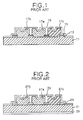
- FIG. 1 is a sectional view showing a structural example of a conventional color filter for a TN mode LCD.
- a first light-shielding layer 13 formed of a metal oxide film and a second light-shielding layer 15 formed of a metal film are disposed in a lattice shape on a transparent substrate 11 .
- the first light-shielding layer 13 may be formed of a twofold film consisting of a metal oxide film and a metal nitride film.
- First, second and third filters 17 a, 17 b and 17 c for transmitting R, G and B color lights, respectively are formed at a portion in which the first and second light-shielding layers 13 and 15 on the transparent substrate 11 are not formed.
- the first, second and third filters 17 a, 17 b and 17 c are made from an acrylic resin or polyimide group resin dispersed with pigments, and is separately formed on the first and second light-shielding layers 13 and 15 to prevent color mixture.
- the common electrode 19 allows the first to third filters 17 a, 17 b and 17 c to not contact a liquid crystal so as to prevent its damage.
- FIG. 2 is a sectional view showing a structural example of a conventional color filter for an IPS mode LCD.
- a light-shielding layer 23 in which a resin dispersed with an electrically insulated black pigment has a lattice shape is formed on transparent substrate 21 .
- First, second and third filters 27 a, 27 b and 27 c for transmitting R, G and B color lights, respectively are formed at a portion in which the light-shielding layer 23 are not formed.
- the first, second and third filters 27 a, 27 b and 27 c are made from an acrylic resin or polyimide group resin dispersed with pigments, and is separately formed on the light-shielding layer 23 so as to prevent color mixture.
- a horizontal electric field generated from the lower plate causes drive problems due to noise generated upon drive control due to a derivative electric field generated by the conductive material.
- a protective layer 25 is formed on the first to third filters 27 a, 27 b and 27 c.
- the protective layer 25 plays a role isolating the first to third filters 27 a, 27 b and 27 c from contact with a liquid crystal (to cause damage thereto), and is made from a transparent material having an insulating characteristic, such as polyimide.
- a ground electrode 29 is formed on the rear surface of the transparent substrate 21 , that is, on the surface in which the first to third filters 27 a, 27 b and 27 c are formed.
- the ground electrode 29 eliminates static electricity on a screen to prevent generation of domain stains, and is made from a transparent conductive material such as ITO, TO or IZO, etc.
- the conventional color filter has a problem in that a step difference is generated at a portion where each of the filters overlaps by a thickness of the light-shielding layer, to cause deterioration in surface morphology.
- the TN mode color filter has a problem in that, when a stacked structure of a metal oxide film and a metal film is formed, pinholes are generated during the cleaning after generation of stripped particles in a continuous film formation process to thereby cause a light leakage phenomenon.
- the IPS mode color filter has a problem in that, since the light-shielding layer is made from only a resin and formed after formation of the ground electrode, a stain is generated due to its contact with a conveyer machine (e.g., a roller and a robot hand, etc.) upon formation of the ground electrode at the rear side of the transparent substrate, or an adhesion between the light-shielding layer and the transparent substrate is weakened to cause stain formation.
- a conveyer machine e.g., a roller and a robot hand, etc.
- a further object of the present invention is to provide a color filter that is capable of preventing light leakage caused by pinholes generated at a light-shielding layer.
- a yet further object of the present invention is to provide a color filter that is capable of preventing stain formation caused by adhesion weakness between a light-shielding layer and a transparent substrate.
- a color filter includes a light-shielding layer having a lattice shape formed from a metal material on a second surface of a transparent substrate having first and second surfaces; and first, second and third filters, being formed at a portion which does not correspond to the light-shielding layer on the first surface of the transparent substrate in such a manner so as to have a desired portion overlapped with the light-shielding layer, to transmit red, green and blue color lights, respectively.
- FIG. 1 is a sectional view showing a structural example of a conventional color filter for a TN mode LCD
- FIG. 2 is a section view showing a structural example of a conventional color filter for an IPS mode LCD
- FIG. 3 is a section view showing a structure of a color filter for a TN mode LCD according to an embodiment of the present invention
- FIG. 4 is a section view showing a structure of a color filter for a IPS mode LCD according to another embodiment of the present invention.
- first and second light-shielding layers 33 and 35 are disposed in a lattice shape on a second surface of a transparent substrate 31 having first and second surfaces.
- the first light-shielding layer 33 is made from a metal such as chromium (Cr) having a thickness of more than 800 ⁇ while the second light-shielding layer 35 is made from a metal oxide such as chromium oxide (Cr 2 O 3 ) having a thickness of 300 to 1000 ⁇ .
- the first and second light-shielding layers 33 and 35 may be formed of a twofold film consisting of a metal oxide film and a metal nitride film. Incident light is reflected from each surface of the first and second light-shielding layers 33 and 35 . Light reflected from each of the surfaces of the first and second light-shielding layers 33 and 35 undergoes extinction interference to prevent progress of the light.
- a third light-shielding layer 37 is formed in a lattice shape on the first surface of the substrate, being opposed to the second surface having the first and second light-shielding layers 33 and 35 .
- the third light-shielding layer 37 is formed from a metal oxide film such as chromium oxide (Cr 2 O 3 ) having a thickness of 300 to 700 ⁇ at a portion opposite to the first and second light-shielding layers 33 and 35 .
- Cr 2 O 3 chromium oxide
- the first to third filters 39 a, 39 b and 39 c for transmitting R, G and B color light, respectively are formed at a portion where the third light-shielding layer 37 on the first surface of the transparent substrate 31 is not formed.
- the first to third filters 39 a, 39 b and 39 c are made from an acrylic or polyimide group resin dispersed with R, G and B pigments and are separately formed on the third light-shielding layer 37 so as to prevent color mixture. Since the third light-shielding layer 37 is formed having a small thickness, the first to third filters 39 a, 39 b and 39 c have a reduced step difference at a portion overlapping with the third light-shielding layer 37 to improve surface morphology.
- a common electrode 41 made from a transparent conductive material such as ITO, TO or IZO is formed on the first to third filters 39 a, 39 b and 39 c.
- the common electrode 41 drives a liquid crystal with a voltage difference from a pixel electrode at a lower plate (not shown). Also, the common electrode 41 prevents the first to third filters 39 a, 39 b and 39 c from contacting the liquid crystal to thereby cause their damage.
- Protective layer 61 made from a transparent insulation material such as an epoxy resin or an acrylic resin, etc. is formed on the first to third filters 59 a, 59 b and 59 c.
- the protective layer 61 prevents the first to third filters 59 a, 59 b and 59 c from contact with a liquid crystal, and thus prevents damage thereto.
- a conductive material layer does not exist on the first surface of the transparent substrate 51 , so that an undesired affect to a horizontal electric field of a lower plate (not shown) is prevented.
- the first light-shielding layer 53 formed from a metal such as a chromium (Cr) on the second surface of the transparent substrate 51 may be used as a ground electrode for eliminating static electricity on a screen.
- the first light-shielding layer 53 is made from a metal while the second and third light-shielding layers 55 and 57 are made from a metal oxide.Stain formation problems are prevented and adhesive force to the transparent substrate 51 is improved.
- FIG. 5A to FIG. 5B represent a process of fabricating the color filter shown in FIG. 3 .
- the first and second light-shielding layers 33 and 35 having a lattice shape are formed on the second surface of the transparent substrate 31 having the first and second surfaces.
- the first and second light-shielding layers 33 and 35 is formed by continuously depositing a metal oxide film such as a twofold film of a metal and a chromium oxide (Cr 2 O 3 ) or a metal nitride film such as a twofold film of a chromium oxide (Cr 2 O 3 ) and a chromium nitride (CrN y O x ) on the second surface of the transparent substrate 31 to a thickness of about 1000 to 2000 ⁇ ,and a thickness of about 300 to 700 ⁇ respectively, using the sputtering technique and then patterning the same using photolithography.
- a metal oxide film such as a twofold film of a metal and a chromium oxide (Cr 2 O 3 ) or a metal nitride film such as a twofold film of a chromium oxide (Cr 2 O 3 ) and a chromium nitride (CrN y O x )
- the third light-shielding layer 37 corresponding to the first and second light-shielding layers 33 and 35 is formed on the first surface of the transparent substrate 31 .
- the third light-shielding layer 37 is formed by depositing a metal oxide film such as chromium oxide (Cr 2 O 3 ) on the first surface of the transparent substrate 31 to a thickness of about 300 to 700 ⁇ using a sputtering technique and then patterning the same using photolithography. At this time, the third light-shielding layer 37 is patterned to correspond to the first and second light-shielding layers 33 and 35 .
- the third light-shielding layer 37 prevents generation of light leakage even though the first and second light-shielding layers 33 and 35 formed on the second surface of the substrate 31 are removed by stripped particles to provide pinholes.
- the first filter 39 A for transmitting only any one of R, G and B color light, for example, only the R color light is provided at a desired portion on the first surface of the transparent substrate 31 .
- the first filter 39 a is formed by coating an acrylic or polyimide group resin dispersed with a R color pigment on the first surface of the transparent substrate 31 and then exposing and developing the same and thereafter patterning the same in such a manner so as to be left only at a desired portion thereof. At this time, the first filter 39 a overlaps with the desired portion of the third light-shielding layer 37 .
- the first filter 39 a Since the third light-shielding layer 37 has a small thickness, the first filter 39 a has a reduced step difference at a portion overlapping with the third light-shielding layer 37 to thereby improve surface morphology in comparison to the case of forming the existent black matrix film of a metal or a resin.
- the second and third filters 39 b and 39 c are continuously formed at a desired portion on the first surface of the transparent substrate 31 in the same manner as the first filter 39 a.
- the second and third filters 39 b and 39 c transmit only G and B color lights except for an R color light in the R, G and B color lights.
- the second and third filters 39 b and 39 c also have a reduced step difference at a portion overlapping with the third light-shielding layer 37 to improve surface morphology.
- the transparent common electrode 41 is formed on the first to third filters 39 a, 39 b and 39 c.
- the common electrode 41 is formed by depositing a transparent conductive material such as ITO, TO or IZO, etc. on the first to third filters 39 a, 39 b and 39 c using a sputtering technique.
- the method of forming the first and second light-shielding layers 53 and 55 having a lattice shape on the second surface of the transparent substrate 51 , and then the third light-shielding layer 57 on the first surface and thereafter form the first to third filters 59 a, 59 b and 59 c on the first surface of the transparent substrate 51 in a method of fabricating the color filter shown in FIG. 4 is similar to the method of fabricating the color filter shown in FIG. 3 .
- the light-shielding layer is formed on the second surface of the transparent substrate to prevent a deterioration of surface morphology. Also, even though the first and second light-shielding layers are removed by stripped particles generated during the continuous deposition process to provide the pinholes, light leakage can be prevented by virtue of the third light-shielding layer.
- the first to third light-shielding layers are made from a metal or a metal oxide, so that it becomes possible to prevent stain formation caused by adhesion weakness between the light-shielding layer and the transparent substrate.
Abstract
Description
Claims (10)
Applications Claiming Priority (3)
| Application Number | Priority Date | Filing Date | Title |
|---|---|---|---|
| KR1019990057571A KR100313248B1 (en) | 1999-12-14 | 1999-12-14 | Color Filter |
| KRP99-57571 | 1999-12-14 | ||
| KR99-57571 | 1999-12-14 |
Publications (2)
| Publication Number | Publication Date |
|---|---|
| US20010053035A1 US20010053035A1 (en) | 2001-12-20 |
| US6469758B2 true US6469758B2 (en) | 2002-10-22 |
Family
ID=19625742
Family Applications (1)
| Application Number | Title | Priority Date | Filing Date |
|---|---|---|---|
| US09/735,512 Expired - Lifetime US6469758B2 (en) | 1999-12-14 | 2000-12-14 | Color filter |
Country Status (2)
| Country | Link |
|---|---|
| US (1) | US6469758B2 (en) |
| KR (1) | KR100313248B1 (en) |
Cited By (14)
| Publication number | Priority date | Publication date | Assignee | Title |
|---|---|---|---|---|
| US20040070706A1 (en) * | 2002-10-10 | 2004-04-15 | Freeman Gary A. | Parallax compensating color filter and black mask for display apparatus |
| US6750929B2 (en) * | 2000-10-31 | 2004-06-15 | Hitachi, Ltd. | Liquid crystal display device |
| US20040179153A1 (en) * | 2003-03-14 | 2004-09-16 | Sheng-Shiou Yeh | Color filter with low reflection and liquid crystal display device having same |
| US20050012445A1 (en) * | 1999-10-12 | 2005-01-20 | Shunpei Yamazaki | EL display device and a method of manufacturing the same |
| US6911772B2 (en) * | 2002-06-12 | 2005-06-28 | Eastman Kodak Company | Oled display having color filters for improving contrast |
| US20060029868A1 (en) * | 2004-08-06 | 2006-02-09 | Innolux Display Corp. | Method and device for manufacturing a color filter |
| US20070026324A1 (en) * | 2005-07-28 | 2007-02-01 | Mitsubishi Electric Corporation | Substrate with light-shielding film, color filter substrate, method of manufacture of both, and display device having substrate with light-shielding film |
| US20080006602A1 (en) * | 2006-07-07 | 2008-01-10 | Innolux Display Corp. | Apparatus and method for fabricating color filter |
| US7494837B2 (en) | 1999-10-13 | 2009-02-24 | Semiconductor Energy Laboratory Co., Ltd. | Thin film forming apparatus |
| US20090167996A1 (en) * | 2007-12-26 | 2009-07-02 | Nec Lcd Technologies, Ltd. | Color filter substrate and liquid crystal display unit |
| CN101526685B (en) * | 2008-03-06 | 2011-07-20 | 北京京东方光电科技有限公司 | Color film substrate and manufacture method thereof |
| WO2014040329A1 (en) * | 2012-09-14 | 2014-03-20 | 深圳市华星光电技术有限公司 | Dual-tft substrate blue phase liquid crystal display panel |
| US9128340B2 (en) | 2012-09-14 | 2015-09-08 | Shenzhen China Star Optoelectronics Technology Co., Ltd. | Dual-TFT-substrate blue-phase liquid crystal display panel |
| US10660754B2 (en) | 2014-07-23 | 2020-05-26 | Clemson University Research Foundation | Self-adjusting tissue holder |
Families Citing this family (4)
| Publication number | Priority date | Publication date | Assignee | Title |
|---|---|---|---|---|
| KR101622184B1 (en) * | 2009-12-28 | 2016-05-19 | 엘지디스플레이 주식회사 | Method of fabricating color filter using surface plasmon and method of fabricating liquid crystal display device |
| CN102645690A (en) * | 2011-05-19 | 2012-08-22 | 京东方科技集团股份有限公司 | Color filter and manufacturing method thereof |
| CN105093668B (en) * | 2015-09-28 | 2018-05-29 | 深圳市华星光电技术有限公司 | A kind of colored filter substrate and its manufacturing method, liquid crystal display panel |
| US20190041701A1 (en) * | 2017-08-01 | 2019-02-07 | Innolux Corporation | Display device |
Citations (3)
| Publication number | Priority date | Publication date | Assignee | Title |
|---|---|---|---|---|
| US4793691A (en) * | 1984-12-25 | 1988-12-27 | Ricoh Company, Ltd. | Liquid crystal color display device |
| JPH0572559A (en) * | 1991-09-17 | 1993-03-26 | Sanyo Electric Co Ltd | Liquid crystal display device |
| US5568292A (en) * | 1992-09-09 | 1996-10-22 | Goldstar Co., Ltd. | Position-sensitive liquid crystal display and process for producing the same |
Family Cites Families (3)
| Publication number | Priority date | Publication date | Assignee | Title |
|---|---|---|---|---|
| JP2799120B2 (en) * | 1993-03-01 | 1998-09-17 | 凸版印刷株式会社 | Color filter and method of manufacturing the same |
| JPH06308319A (en) * | 1993-04-27 | 1994-11-04 | Kyocera Corp | Production of color filter |
| JPH08262219A (en) * | 1995-03-28 | 1996-10-11 | Toshiba Corp | Color filter |
-
1999
- 1999-12-14 KR KR1019990057571A patent/KR100313248B1/en not_active IP Right Cessation
-
2000
- 2000-12-14 US US09/735,512 patent/US6469758B2/en not_active Expired - Lifetime
Patent Citations (3)
| Publication number | Priority date | Publication date | Assignee | Title |
|---|---|---|---|---|
| US4793691A (en) * | 1984-12-25 | 1988-12-27 | Ricoh Company, Ltd. | Liquid crystal color display device |
| JPH0572559A (en) * | 1991-09-17 | 1993-03-26 | Sanyo Electric Co Ltd | Liquid crystal display device |
| US5568292A (en) * | 1992-09-09 | 1996-10-22 | Goldstar Co., Ltd. | Position-sensitive liquid crystal display and process for producing the same |
Cited By (25)
| Publication number | Priority date | Publication date | Assignee | Title |
|---|---|---|---|---|
| US7521722B2 (en) * | 1999-10-12 | 2009-04-21 | Semiconductor Energy Laboratory Co., Ltd. | EL display device and a method of manufacturing the same |
| US8133748B2 (en) | 1999-10-12 | 2012-03-13 | Semiconductor Energy Laboratory Co., Ltd. | EL display device and method of manufacturing the same |
| US20050012445A1 (en) * | 1999-10-12 | 2005-01-20 | Shunpei Yamazaki | EL display device and a method of manufacturing the same |
| US7989812B2 (en) | 1999-10-12 | 2011-08-02 | Semiconductor Energy Laboratory Co., Ltd. | EL display device and a method of manufacturing the same |
| US8319224B2 (en) | 1999-10-12 | 2012-11-27 | Semiconductor Energy Laboratory Co., Ltd. | EL display device and a method of manufacturing the same |
| US8884301B2 (en) | 1999-10-12 | 2014-11-11 | Semiconductor Energy Laboratory Co., Ltd. | EL display device and a method of manufacturing the same |
| US7548023B2 (en) | 1999-10-12 | 2009-06-16 | Semiconductor Energy Laboratory Co., Ltd. | EL display device and a method of manufacturing the same |
| US7473928B1 (en) | 1999-10-12 | 2009-01-06 | Semiconductor Energy Laboratory Co., Ltd. | EL display device and a method of manufacturing the same |
| US7919341B2 (en) | 1999-10-13 | 2011-04-05 | Semiconductor Energy Laboratory Co., Ltd. | Thin film forming apparatus |
| US7494837B2 (en) | 1999-10-13 | 2009-02-24 | Semiconductor Energy Laboratory Co., Ltd. | Thin film forming apparatus |
| US6750929B2 (en) * | 2000-10-31 | 2004-06-15 | Hitachi, Ltd. | Liquid crystal display device |
| US6911772B2 (en) * | 2002-06-12 | 2005-06-28 | Eastman Kodak Company | Oled display having color filters for improving contrast |
| US7388631B2 (en) * | 2002-10-10 | 2008-06-17 | Samsung Electronics, Co., Ltd. | Parallax compensating color filter and black mask for display apparatus |
| US20040070706A1 (en) * | 2002-10-10 | 2004-04-15 | Freeman Gary A. | Parallax compensating color filter and black mask for display apparatus |
| US20040179153A1 (en) * | 2003-03-14 | 2004-09-16 | Sheng-Shiou Yeh | Color filter with low reflection and liquid crystal display device having same |
| US20060029868A1 (en) * | 2004-08-06 | 2006-02-09 | Innolux Display Corp. | Method and device for manufacturing a color filter |
| US20070026324A1 (en) * | 2005-07-28 | 2007-02-01 | Mitsubishi Electric Corporation | Substrate with light-shielding film, color filter substrate, method of manufacture of both, and display device having substrate with light-shielding film |
| US20080006602A1 (en) * | 2006-07-07 | 2008-01-10 | Innolux Display Corp. | Apparatus and method for fabricating color filter |
| US8269924B2 (en) * | 2007-12-26 | 2012-09-18 | Nlt Technologies, Ltd. | Color filter substrate and liquid crystal display unit |
| US20090167996A1 (en) * | 2007-12-26 | 2009-07-02 | Nec Lcd Technologies, Ltd. | Color filter substrate and liquid crystal display unit |
| US8411233B2 (en) | 2007-12-26 | 2013-04-02 | Nec Lcd Technologies, Ltd. | Method for manufacturing a color filter substrate |
| CN101526685B (en) * | 2008-03-06 | 2011-07-20 | 北京京东方光电科技有限公司 | Color film substrate and manufacture method thereof |
| WO2014040329A1 (en) * | 2012-09-14 | 2014-03-20 | 深圳市华星光电技术有限公司 | Dual-tft substrate blue phase liquid crystal display panel |
| US9128340B2 (en) | 2012-09-14 | 2015-09-08 | Shenzhen China Star Optoelectronics Technology Co., Ltd. | Dual-TFT-substrate blue-phase liquid crystal display panel |
| US10660754B2 (en) | 2014-07-23 | 2020-05-26 | Clemson University Research Foundation | Self-adjusting tissue holder |
Also Published As
| Publication number | Publication date |
|---|---|
| KR20010056136A (en) | 2001-07-04 |
| KR100313248B1 (en) | 2001-11-07 |
| US20010053035A1 (en) | 2001-12-20 |
Similar Documents
| Publication | Publication Date | Title |
|---|---|---|
| US6469758B2 (en) | Color filter | |
| KR101085132B1 (en) | Thin film transistor substrate of horizontal electric field and fabricating method thereof | |
| KR101167304B1 (en) | Thin film transistor substrate of fringe field switch type and fabricating method thereof | |
| KR101125254B1 (en) | Thin Film Transistor Substrate of Fringe Field Switching Type And Fabricating Method Thereof, Liquid Crystal Display Panel Using The Same And Fabricating Method Thereof | |
| KR101085136B1 (en) | Thin film transistor substrate of horizontal electric field and fabricating method thereof | |
| US7667807B2 (en) | In-plane-switching-mode liquid crystal display device | |
| KR100266151B1 (en) | Transmission type liquid crystal display device and method for fabricating the same | |
| JP2974520B2 (en) | Electrode substrate and liquid crystal element | |
| US20070155080A1 (en) | Thim film transistor substrate and manufacturing method thereof | |
| KR101085142B1 (en) | Thin film transistor substrate of horizontal electric field and fabricating method thereof | |
| US6556263B2 (en) | In-plane switching color LCD panel implementing electro-conductive polarizer and fabricating method thereof | |
| US7894010B2 (en) | Liquid crystal display panel and method for fabricating the same | |
| KR20080077831A (en) | Liquid crystal display panel of horizontal electronic field applying type and method for fabricating thereof | |
| KR20060079033A (en) | Thin film transistor substrate of horizontal electric field and fabricating method thereof, liquid crystal display panel using the same and fabricating method thereof | |
| KR20090104146A (en) | Thin Film Transistor Substrate of Horizontal Electric Field And Fabricating Method Thereof, Liquid Crystal Display Panel Using The Same And Fabricating Method Thereof | |
| KR101157222B1 (en) | Liquid crystal display panel of horizontal electronic field applying type and fabricating method thereof | |
| JPH0968723A (en) | Liquid crystal display device | |
| KR101127822B1 (en) | Thin film transistor substrate of horizontal electric field and fabricating method thereof | |
| KR101096718B1 (en) | Fabricating method of thin film transistor substrate of horizontal electric field | |
| US8264644B2 (en) | Color filter substrate for in-plane switching mode liquid crystal display device and method of fabricating the same | |
| JP3403931B2 (en) | Liquid crystal display | |
| KR100413512B1 (en) | an array panel for liquid crystal display and manufacturing method thereof | |
| KR101208972B1 (en) | In plane switching mode liquid crystal display device and method of fabricating thereof | |
| KR20080054629A (en) | Thin film transistor array substrate and manufacturing method thereof | |
| KR20160028074A (en) | Thin film transistor substrate and display panel having the same |
Legal Events
| Date | Code | Title | Description |
|---|---|---|---|
| AS | Assignment |
Owner name: SONY CORPORATION, JAPAN Free format text: ASSIGNMENT OF ASSIGNORS INTEREST;ASSIGNORS:EDWARDS, ERIC;FISHER, CLAY HARVEY;REEL/FRAME:011367/0293;SIGNING DATES FROM 20001128 TO 20001206 Owner name: SONY ELECTRONICS, INC., NEW JERSEY Free format text: ASSIGNMENT OF ASSIGNORS INTEREST;ASSIGNORS:EDWARDS, ERIC;FISHER, CLAY HARVEY;REEL/FRAME:011367/0293;SIGNING DATES FROM 20001128 TO 20001206 |
|
| AS | Assignment |
Owner name: L.G. PHILIPS LCG CO., LTD., KOREA, REPUBLIC OF Free format text: ASSIGNMENT OF ASSIGNORS INTEREST;ASSIGNOR:YU, JUN YOUNG;REEL/FRAME:011661/0573 Effective date: 20010312 |
|
| AS | Assignment |
Owner name: L.G. PHILIPS LCD CO., LTD., KOREA, REPUBLIC OF Free format text: RE-RECORD TO CORRECT THE ASSIGNEE'S NAME, PREVIOUSLY RECORDED AT REEL 011661, FRAME 0573.;ASSIGNOR:YU, JUN YOUNG;REEL/FRAME:011945/0530 Effective date: 20010312 |
|
| STCF | Information on status: patent grant |
Free format text: PATENTED CASE |
|
| FPAY | Fee payment |
Year of fee payment: 4 |
|
| AS | Assignment |
Owner name: LG DISPLAY CO., LTD., KOREA, REPUBLIC OF Free format text: CHANGE OF NAME;ASSIGNOR:LG.PHILIPS LCD CO., LTD.;REEL/FRAME:020985/0675 Effective date: 20080304 Owner name: LG DISPLAY CO., LTD.,KOREA, REPUBLIC OF Free format text: CHANGE OF NAME;ASSIGNOR:LG.PHILIPS LCD CO., LTD.;REEL/FRAME:020985/0675 Effective date: 20080304 |
|
| FEPP | Fee payment procedure |
Free format text: PAYOR NUMBER ASSIGNED (ORIGINAL EVENT CODE: ASPN); ENTITY STATUS OF PATENT OWNER: LARGE ENTITY |
|
| FPAY | Fee payment |
Year of fee payment: 8 |
|
| FPAY | Fee payment |
Year of fee payment: 12 |