US6475813B1 - MOCVD and annealing processes for C-axis oriented ferroelectric thin films - Google Patents
MOCVD and annealing processes for C-axis oriented ferroelectric thin films Download PDFInfo
- Publication number
- US6475813B1 US6475813B1 US09/929,711 US92971101A US6475813B1 US 6475813 B1 US6475813 B1 US 6475813B1 US 92971101 A US92971101 A US 92971101A US 6475813 B1 US6475813 B1 US 6475813B1
- Authority
- US
- United States
- Prior art keywords
- depositing
- ferroelectric material
- minutes
- ferroelectric
- temperature
- Prior art date
- Legal status (The legal status is an assumption and is not a legal conclusion. Google has not performed a legal analysis and makes no representation as to the accuracy of the status listed.)
- Expired - Lifetime
Links
Images

Classifications
-
- H—ELECTRICITY
- H01—ELECTRIC ELEMENTS
- H01L—SEMICONDUCTOR DEVICES NOT COVERED BY CLASS H10
- H01L27/00—Devices consisting of a plurality of semiconductor or other solid-state components formed in or on a common substrate
- H01L27/02—Devices consisting of a plurality of semiconductor or other solid-state components formed in or on a common substrate including semiconductor components specially adapted for rectifying, oscillating, amplifying or switching and having at least one potential-jump barrier or surface barrier; including integrated passive circuit elements with at least one potential-jump barrier or surface barrier
- H01L27/04—Devices consisting of a plurality of semiconductor or other solid-state components formed in or on a common substrate including semiconductor components specially adapted for rectifying, oscillating, amplifying or switching and having at least one potential-jump barrier or surface barrier; including integrated passive circuit elements with at least one potential-jump barrier or surface barrier the substrate being a semiconductor body
- H01L27/10—Devices consisting of a plurality of semiconductor or other solid-state components formed in or on a common substrate including semiconductor components specially adapted for rectifying, oscillating, amplifying or switching and having at least one potential-jump barrier or surface barrier; including integrated passive circuit elements with at least one potential-jump barrier or surface barrier the substrate being a semiconductor body including a plurality of individual components in a repetitive configuration
- H01L27/105—Devices consisting of a plurality of semiconductor or other solid-state components formed in or on a common substrate including semiconductor components specially adapted for rectifying, oscillating, amplifying or switching and having at least one potential-jump barrier or surface barrier; including integrated passive circuit elements with at least one potential-jump barrier or surface barrier the substrate being a semiconductor body including a plurality of individual components in a repetitive configuration including field-effect components
-
- C—CHEMISTRY; METALLURGY
- C23—COATING METALLIC MATERIAL; COATING MATERIAL WITH METALLIC MATERIAL; CHEMICAL SURFACE TREATMENT; DIFFUSION TREATMENT OF METALLIC MATERIAL; COATING BY VACUUM EVAPORATION, BY SPUTTERING, BY ION IMPLANTATION OR BY CHEMICAL VAPOUR DEPOSITION, IN GENERAL; INHIBITING CORROSION OF METALLIC MATERIAL OR INCRUSTATION IN GENERAL
- C23C—COATING METALLIC MATERIAL; COATING MATERIAL WITH METALLIC MATERIAL; SURFACE TREATMENT OF METALLIC MATERIAL BY DIFFUSION INTO THE SURFACE, BY CHEMICAL CONVERSION OR SUBSTITUTION; COATING BY VACUUM EVAPORATION, BY SPUTTERING, BY ION IMPLANTATION OR BY CHEMICAL VAPOUR DEPOSITION, IN GENERAL
- C23C16/00—Chemical coating by decomposition of gaseous compounds, without leaving reaction products of surface material in the coating, i.e. chemical vapour deposition [CVD] processes
- C23C16/22—Chemical coating by decomposition of gaseous compounds, without leaving reaction products of surface material in the coating, i.e. chemical vapour deposition [CVD] processes characterised by the deposition of inorganic material, other than metallic material
- C23C16/30—Deposition of compounds, mixtures or solid solutions, e.g. borides, carbides, nitrides
- C23C16/40—Oxides
-
- C—CHEMISTRY; METALLURGY
- C30—CRYSTAL GROWTH
- C30B—SINGLE-CRYSTAL GROWTH; UNIDIRECTIONAL SOLIDIFICATION OF EUTECTIC MATERIAL OR UNIDIRECTIONAL DEMIXING OF EUTECTOID MATERIAL; REFINING BY ZONE-MELTING OF MATERIAL; PRODUCTION OF A HOMOGENEOUS POLYCRYSTALLINE MATERIAL WITH DEFINED STRUCTURE; SINGLE CRYSTALS OR HOMOGENEOUS POLYCRYSTALLINE MATERIAL WITH DEFINED STRUCTURE; AFTER-TREATMENT OF SINGLE CRYSTALS OR A HOMOGENEOUS POLYCRYSTALLINE MATERIAL WITH DEFINED STRUCTURE; APPARATUS THEREFOR
- C30B25/00—Single-crystal growth by chemical reaction of reactive gases, e.g. chemical vapour-deposition growth
- C30B25/02—Epitaxial-layer growth
-
- C—CHEMISTRY; METALLURGY
- C30—CRYSTAL GROWTH
- C30B—SINGLE-CRYSTAL GROWTH; UNIDIRECTIONAL SOLIDIFICATION OF EUTECTIC MATERIAL OR UNIDIRECTIONAL DEMIXING OF EUTECTOID MATERIAL; REFINING BY ZONE-MELTING OF MATERIAL; PRODUCTION OF A HOMOGENEOUS POLYCRYSTALLINE MATERIAL WITH DEFINED STRUCTURE; SINGLE CRYSTALS OR HOMOGENEOUS POLYCRYSTALLINE MATERIAL WITH DEFINED STRUCTURE; AFTER-TREATMENT OF SINGLE CRYSTALS OR A HOMOGENEOUS POLYCRYSTALLINE MATERIAL WITH DEFINED STRUCTURE; APPARATUS THEREFOR
- C30B29/00—Single crystals or homogeneous polycrystalline material with defined structure characterised by the material or by their shape
- C30B29/10—Inorganic compounds or compositions
- C30B29/16—Oxides
- C30B29/22—Complex oxides
- C30B29/30—Niobates; Vanadates; Tantalates
-
- C—CHEMISTRY; METALLURGY
- C30—CRYSTAL GROWTH
- C30B—SINGLE-CRYSTAL GROWTH; UNIDIRECTIONAL SOLIDIFICATION OF EUTECTIC MATERIAL OR UNIDIRECTIONAL DEMIXING OF EUTECTOID MATERIAL; REFINING BY ZONE-MELTING OF MATERIAL; PRODUCTION OF A HOMOGENEOUS POLYCRYSTALLINE MATERIAL WITH DEFINED STRUCTURE; SINGLE CRYSTALS OR HOMOGENEOUS POLYCRYSTALLINE MATERIAL WITH DEFINED STRUCTURE; AFTER-TREATMENT OF SINGLE CRYSTALS OR A HOMOGENEOUS POLYCRYSTALLINE MATERIAL WITH DEFINED STRUCTURE; APPARATUS THEREFOR
- C30B29/00—Single crystals or homogeneous polycrystalline material with defined structure characterised by the material or by their shape
- C30B29/10—Inorganic compounds or compositions
- C30B29/16—Oxides
- C30B29/22—Complex oxides
- C30B29/32—Titanates; Germanates; Molybdates; Tungstates
-
- H—ELECTRICITY
- H01—ELECTRIC ELEMENTS
- H01L—SEMICONDUCTOR DEVICES NOT COVERED BY CLASS H10
- H01L21/00—Processes or apparatus adapted for the manufacture or treatment of semiconductor or solid state devices or of parts thereof
- H01L21/02—Manufacture or treatment of semiconductor devices or of parts thereof
- H01L21/02104—Forming layers
- H01L21/02107—Forming insulating materials on a substrate
- H01L21/02109—Forming insulating materials on a substrate characterised by the type of layer, e.g. type of material, porous/non-porous, pre-cursors, mixtures or laminates
- H01L21/02112—Forming insulating materials on a substrate characterised by the type of layer, e.g. type of material, porous/non-porous, pre-cursors, mixtures or laminates characterised by the material of the layer
- H01L21/02172—Forming insulating materials on a substrate characterised by the type of layer, e.g. type of material, porous/non-porous, pre-cursors, mixtures or laminates characterised by the material of the layer the material containing at least one metal element, e.g. metal oxides, metal nitrides, metal oxynitrides or metal carbides
- H01L21/02197—Forming insulating materials on a substrate characterised by the type of layer, e.g. type of material, porous/non-porous, pre-cursors, mixtures or laminates characterised by the material of the layer the material containing at least one metal element, e.g. metal oxides, metal nitrides, metal oxynitrides or metal carbides the material having a perovskite structure, e.g. BaTiO3
-
- H—ELECTRICITY
- H01—ELECTRIC ELEMENTS
- H01L—SEMICONDUCTOR DEVICES NOT COVERED BY CLASS H10
- H01L21/00—Processes or apparatus adapted for the manufacture or treatment of semiconductor or solid state devices or of parts thereof
- H01L21/02—Manufacture or treatment of semiconductor devices or of parts thereof
- H01L21/02104—Forming layers
- H01L21/02107—Forming insulating materials on a substrate
- H01L21/02109—Forming insulating materials on a substrate characterised by the type of layer, e.g. type of material, porous/non-porous, pre-cursors, mixtures or laminates
- H01L21/02205—Forming insulating materials on a substrate characterised by the type of layer, e.g. type of material, porous/non-porous, pre-cursors, mixtures or laminates the layer being characterised by the precursor material for deposition
-
- H—ELECTRICITY
- H01—ELECTRIC ELEMENTS
- H01L—SEMICONDUCTOR DEVICES NOT COVERED BY CLASS H10
- H01L21/00—Processes or apparatus adapted for the manufacture or treatment of semiconductor or solid state devices or of parts thereof
- H01L21/02—Manufacture or treatment of semiconductor devices or of parts thereof
- H01L21/02104—Forming layers
- H01L21/02107—Forming insulating materials on a substrate
- H01L21/02225—Forming insulating materials on a substrate characterised by the process for the formation of the insulating layer
- H01L21/0226—Forming insulating materials on a substrate characterised by the process for the formation of the insulating layer formation by a deposition process
- H01L21/02263—Forming insulating materials on a substrate characterised by the process for the formation of the insulating layer formation by a deposition process deposition from the gas or vapour phase
- H01L21/02271—Forming insulating materials on a substrate characterised by the process for the formation of the insulating layer formation by a deposition process deposition from the gas or vapour phase deposition by decomposition or reaction of gaseous or vapour phase compounds, i.e. chemical vapour deposition
-
- H—ELECTRICITY
- H01—ELECTRIC ELEMENTS
- H01L—SEMICONDUCTOR DEVICES NOT COVERED BY CLASS H10
- H01L21/00—Processes or apparatus adapted for the manufacture or treatment of semiconductor or solid state devices or of parts thereof
- H01L21/02—Manufacture or treatment of semiconductor devices or of parts thereof
- H01L21/02104—Forming layers
- H01L21/02107—Forming insulating materials on a substrate
- H01L21/02296—Forming insulating materials on a substrate characterised by the treatment performed before or after the formation of the layer
- H01L21/02318—Forming insulating materials on a substrate characterised by the treatment performed before or after the formation of the layer post-treatment
- H01L21/02356—Forming insulating materials on a substrate characterised by the treatment performed before or after the formation of the layer post-treatment treatment to change the morphology of the insulating layer, e.g. transformation of an amorphous layer into a crystalline layer
-
- H—ELECTRICITY
- H01—ELECTRIC ELEMENTS
- H01L—SEMICONDUCTOR DEVICES NOT COVERED BY CLASS H10
- H01L21/00—Processes or apparatus adapted for the manufacture or treatment of semiconductor or solid state devices or of parts thereof
- H01L21/02—Manufacture or treatment of semiconductor devices or of parts thereof
- H01L21/04—Manufacture or treatment of semiconductor devices or of parts thereof the devices having at least one potential-jump barrier or surface barrier, e.g. PN junction, depletion layer or carrier concentration layer
- H01L21/18—Manufacture or treatment of semiconductor devices or of parts thereof the devices having at least one potential-jump barrier or surface barrier, e.g. PN junction, depletion layer or carrier concentration layer the devices having semiconductor bodies comprising elements of Group IV of the Periodic System or AIIIBV compounds with or without impurities, e.g. doping materials
- H01L21/30—Treatment of semiconductor bodies using processes or apparatus not provided for in groups H01L21/20 - H01L21/26
- H01L21/31—Treatment of semiconductor bodies using processes or apparatus not provided for in groups H01L21/20 - H01L21/26 to form insulating layers thereon, e.g. for masking or by using photolithographic techniques; After treatment of these layers; Selection of materials for these layers
- H01L21/314—Inorganic layers
- H01L21/316—Inorganic layers composed of oxides or glassy oxides or oxide based glass
- H01L21/31604—Deposition from a gas or vapour
-
- H—ELECTRICITY
- H01—ELECTRIC ELEMENTS
- H01L—SEMICONDUCTOR DEVICES NOT COVERED BY CLASS H10
- H01L21/00—Processes or apparatus adapted for the manufacture or treatment of semiconductor or solid state devices or of parts thereof
- H01L21/02—Manufacture or treatment of semiconductor devices or of parts thereof
- H01L21/04—Manufacture or treatment of semiconductor devices or of parts thereof the devices having at least one potential-jump barrier or surface barrier, e.g. PN junction, depletion layer or carrier concentration layer
- H01L21/18—Manufacture or treatment of semiconductor devices or of parts thereof the devices having at least one potential-jump barrier or surface barrier, e.g. PN junction, depletion layer or carrier concentration layer the devices having semiconductor bodies comprising elements of Group IV of the Periodic System or AIIIBV compounds with or without impurities, e.g. doping materials
- H01L21/30—Treatment of semiconductor bodies using processes or apparatus not provided for in groups H01L21/20 - H01L21/26
- H01L21/31—Treatment of semiconductor bodies using processes or apparatus not provided for in groups H01L21/20 - H01L21/26 to form insulating layers thereon, e.g. for masking or by using photolithographic techniques; After treatment of these layers; Selection of materials for these layers
- H01L21/314—Inorganic layers
- H01L21/316—Inorganic layers composed of oxides or glassy oxides or oxide based glass
- H01L21/31691—Inorganic layers composed of oxides or glassy oxides or oxide based glass with perovskite structure
Abstract
A method of fabricating a c-axis ferroelectric thin film includes preparing a substrate; depositing a layer of ferroelectric material by metal organic chemical vapor deposition, including using a precursor solution having a ferroelectric material concentration of about 0.1 M/L at a vaporizer temperature of between about 140° C. to 200° C.; and annealing the substrate and the ferroelectric material at a temperature between about 500° C. to 560° C. for between about 30 minutes to 120 minutes.
Description
This invention relates to the fabrication of ferroelectric memory devices, and more particularly to the use of specifically oriented ferroelectric thin films which exhibit both very good ferroelectric properties and lower surface roughness.
The use of ferroelectric thin films in non-volatile memories has drawn much attention in recent years, primarily due to the bi-stable nature of these films, i.e., these films have two predominant polarization directions. Most of the studies of Ferroelectric Random Access Memories (FRAMs) have concentrated on structures having one transistor and one capacitor. The capacitor is made of a thin ferroelectric film sandwiched between two conductive electrodes. The circuit configuration and read/write sequence of this type memory are similar to that of DRAMs, except that data refreshing is not necessary in FRAMs.
Another aspect of ferroelectric non-volatile memory formation is to determine the best technique for deposition of a ferroelectric thin film directly onto the gate area of a FET and to form a ferroelectric-gate controlled FET (FGCFET). Ferroelectric-gate-controlled devices, such as metal-ferroelectric-silicon (MFS) FETs, have been proposed as early as the 1950s, and various modified MFSFET structures have been proposed, for example, metal-ferroelectric-insulator-silicon (MFIS) FETs, metal-ferroelectric-metal-silicon (MFMS) FETs, and metal-ferroelectric-metal-oxide-silicon (MFMOS) FETs.
In order to meet the requirements of FRAMs applications, however, specifically oriented ferroelectric thin films are needed. Experimental results demonstrate that, using metal organic chemical vapor deposition (MOCVD) processes, high oriented, i.e., wherein the ration of c-axis peak-to-random peak is larger than 80%, ferroelectric thin films always have an unacceptable surface roughness because of the growth process using MOCVD.
A method of fabricating a c-axis ferroelectric thin film includes preparing a substrate; depositing a layer of ferroelectric material by metal organic chemical vapor deposition, including using a precursor solution having a ferroelectric material concentration of about 0.1 M/L at a vaporizer temperature of between about 140° C. to 200° C.; and annealing the substrate and the ferroelectric material at a temperature between about 500° C. to 560° C. for between about 30 minutes to 120 minutes.
An object of the invention is to provide fabrication processes, such as MOCVD and annealing, for ferroelectric thin films having a preferred orientation.
Another object of the invention is to provide a ferroelectric thin film having minimal surface roughness, uniform surface morphology and improved ferroelectric properties through the use of multiple MOCVD and annealing processes.
This summary and objectives of the invention are provided to enable quick comprehension of the nature of the invention. A more thorough understanding of the invention may be obtained by reference to the following detailed description of the preferred embodiment of the invention in connection with the drawings.
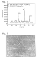
FIG. 1 depicts X-ray patterns of PGO thin films on Ir electrodes made by the MOCVD and annealing process of the method of the invention.
FIG. 2 depicts the microstructures of PGO thin films on Ir electrodes made by the method of the invention.
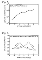
FIG. 3 depicts the hysteresis loop of PGO thin film on Ir electrodes made by the method of the invention.
FIG. 4 depicts the hysteresis loops of PGO thin film on Ir electrodes made by the method of the invention at various applied voltages.
FIG. 5 depicts the leakage current of PGO thin film on Ir electrodes made by the method of the invention.
FIG. 6 depicts the dielectric constants of PGO thin film on Ir electrodes made by the method of the invention.
In this invention, a metal organic chemical vapor deposition (MOCVD) and annealing processes is disclosed, which results in high quality, specifically oriented ferroelectric thin films having low surface roughness. Ferroelectric materials which are suitable for use in the method of the invention include Pb5Ge3O11 (PGO), SrBi2Ta2O9 (SBT), Bi4Ti3O12 (BTO) and PbZrXTi1−XO3 (PZT).
The method of the invention provides a technique to deposit ferroelectric thin films having a preferred orientation, which results in improved surface smoothness, better surface morphology and which maintains desirable properties of an oriented ferroelectric thin film. Extremely high c-axis oriented PGO thin films demonstrate excellent ferroelectric properties, however, the surface of the PGO thin films exhibits a rough character, which creates imperfections in overlaying layers and results in inconsistent conductivity. In order to solve this problem, a low temperature MOCVD step and a high temperature annealing step are used, which results in high quality specifically oriented ferroelectric thin films having relatively smooth surfaces.
An oxide MOCVD reactor is used for the growth of c-axis oriented PGO thin films. A precursor solution of [Pb(thd)2] and [Ge(ETO)4], in a molar ratio of 5:3, is dissolved in a mixed solvent of butyl ether or tetrahydrofuran, isopropanol and tetraglyme, in a molar ratio of 8:2:1. The precursor solutions has a concentration of 0.1 mole-per-liter (M/L) of PGO. The solution is injected into a vaporizer at a temperature of between about 140° C. to 200° C., by a pump at a rate of between about 0.1 ml/min to 0.2 ml/min to form the precursor gases. The temperature of the growth line is between about 165° C. to 245° C. The deposition temperatures and pressure are between about 300° C. and 450° C. and 5 torr to 10 torr, respectively. An argon shroud gas has a flow of between about 1000 sccm to 6000 sccm, and an oxygen partial pressure of between about 20% to 50%. Deposition times of between 30 to 120 minutes are used for growth of PGO thin films on an Ir electrode. As used herein, “low temperature” is defined as a temperature <500° C., as PGO thin films are nearly amorphous at such temperatures. As the temperature rises above 500° C., and particularly above 510° C., the thin films become crystalline.
After PGO film deposition, high temperature annealing processes are used to further promote fine grain growth of the PGO thin films, at temperatures between about 500° C. to 560° C., for between about 30 minutes to 120 minutes. The processes are repeated to form multiple layers of high quality PGO thin films.
FIG. 1 depicts the X-ray pattern of c-axis oriented PGO thin films made by the low temperature MOCVD and high temperature annealing steps of the method of the invention. The PGO thin film has very high c-axis orientation of Pb5Ge3O11, and very little of the second phase Pb3GeO5. FIG. 2 depicts the microstructure of a c-axis oriented PGO thin films formed by the MOCVD and annealing steps of the method of the invention. The average grain size of the PGO film is about 0.8 μm. The existence of the layered structure confirms that the c-axis oriented PGO thin films grew layer-by-layer along the c-axis direction. The layered structure is depicted by the scale-like appearance in the microphotograph of FIG. 2, which has been partially enhanced on the right side thereof to better show the layering. The thickness of PGO thin film is measured at about 300 nm.
PGO thin films made by the method of the invention exhibit very good ferroelectric and electrical properties. FIG. 3 depicts the hysteresis loop of the PGO thin film, which is square, symmetrical and well saturated, at an applied voltage of 5 volts, wherein voltage is on the x-axis and polarization (μC/cm2) is on the y-axis. The 2Pr of 3.98 μC/cm2, and the 2Ec of 128 KV/cm are obtained for the PGO film. FIG. 4 depicts the hysteresis loops of the PGO thin films, generally at 10. Traces are shown for one volt, 12; two volts, 14; three volts, 16; four volts, 18; and five volts, 20. The hysteresis loops of the PGO thin film are nearly saturated from 3 volts.
A low leakage current density is an important consideration for memory device applications. FIG. 5 depicts the I-V curve of a 300 nm thick MOCVD PGO thin film formed according to the method of the invention. Excellent I-V characteristics are present. The leakage current density of the Pb5Ge3O11 thin films increases with increasing applied voltage, and is about 5.07×10⁻⁷ A/cm2 at 100 KV/cm.
The dielectric constant is also another important consideration for a memory device, especially for one transistor memory applications. The dielectric constant of Pb5Ge3O11 thin films exhibits similar behavior to most ferroelectric materials, i.e., the dielectric constant changes with applied voltage. The maximum dielectric constant of the Pb5Ge3O11 thin films is about 36, as shown is FIG. 6.
In summary, a process of low temperature MOCVD of ferroelectric material and high temperature annealing produces a c-axis oriented PGO thin film having reducing the surface roughness. The method of the invention produces high quality PGO thin films on Ir electrodes having a 2Pr of 3.98 μC/cm2 and a 2Ec of 128 kV/cm.
Thus, a method for low temperature ferroelectric MOCVD and annealing for c-axis oriented ferroelectric thin films has been disclosed. It will be appreciated that further variations and modifications thereof may be made within the scope of the invention as defined in the appended claims.
Claims (22)
1. A method of fabricating a c-axis ferroelectric thin film comprising:
preparing a substrate;
depositing a layer of amorphous ferroelectric material by metal organic chemical vapor deposition, including using a precursor solution having a ferroelectric material concentration of about 0.1 M/L at a vaporizer temperature of between about 140° C. to 200° C.; and
annealing the substrate and the ferroelectric material at a temperature between about 500° C. to 560° C. for between about 30 minutes to 120 minutes to produce an amorphous ferroelectric thin film having a grain size of about 0.8 μm.
2. The method of claim 1 wherein said depositing includes selecting a ferroelectric material from the group of materials consisting of Pb5Ge3O11 (PGO), SrBi2Ta2O9 (SBT), Bi4Ti3O12 (BTO) and PbZrXTi1−XO3 (PZT).
3. The method of claim 1 wherein said depositing includes preparing a precursor solution of [Pb(thd)2] and [Ge(ETO)4], in a molar ratio of 5:3, dissolved in a mixed solvent including a solvent taken from the group of solvents consisting of butyl ether and tetrahydrofuran, isopropanol and tetraglyme, in a molar ratio of 8:2:1.
4. The method of claim 1 wherein said depositing includes providing the precursor solution at a pump rate of between about 0.1 ml/min and 0.2 ml/min.
5. The method of claim 1 wherein said depositing includes providing a growth line temperature in the MOCVD chamber of between about 165° C. and 245° C.
6. The method of claim 1 wherein said depositing includes depositing the ferroelectric material at a deposition temperature of between about 300° C. and 450° C.
7. The method of claim 1 wherein said depositing includes depositing the ferroelectric material at a deposition pressure of between about 5 torr. to 10 torr.
8. The method of claim 1 wherein said depositing includes providing a shroud gas of argon at a flow of between about 1000 sccm to 6000 sccm and an oxygen partial pressure of between about 20% to 50%.
9. The method of claim 1 wherein said depositing includes depositing the ferroelectric material over a time period of between about 30 minutes and 120 minutes.
10. A method of fabricating a c-axis ferroelectric thin film comprising:
preparing a substrate;
depositing a layer of amorphous ferroelectric material in a MOCVD chamber at a deposition temperature of between about 300° C. and 450° C. from the group of materials consisting of Pb5Ge3O11 (PGO), SrBi2Ta2O9 (SBT), Bi4Ti3O12 (BTO) and PbZrXTi1−XO3 (PZT) by metal organic chemical vapor deposition, including using a precursor solution having a ferroelectric material concentration of about 0.1 M/L at a vaporizer temperature of between about 140° C. to 200° C. to produce an amorphous ferroelectric thin film having a grain size of about 0.8 μm; and
annealing the substrate and the ferroelectric material at a temperature between about 500° C. to 560° C. for between about 30 minutes to 120 minutes.
11. The method of claim 10 wherein said depositing includes preparing a precursor solution of [Pb(thd)2] and [Ge(ETO)4], in a molar ratio of 5:3, dissolved in a mixed solvent including a solvent taken from the group of solvents consisting of butyl ether and tetrahydrofuran, isopropanol and tetraglyme, in a molar ratio of 8:2:1, and providing the precursor solution at a pump rate of between about 0.1 ml/min and 0.2 ml/min.
12. The method of claim 10 wherein said depositing includes providing a growth line temperature in the MOCVD chamber of between about 165° C. and 245° C.
13. The method of claim 10 wherein said depositing includes depositing the ferroelectric material at a deposition pressure of between about 5 torr. to 10 torr.
14. The method of claim 10 wherein said depositing includes providing a shroud gas of argon at a flow of between about 1000 sccm to 6000 sccm and an oxygen partial pressure of between about 20% to 50%.
15. The method of claim 10 wherein said depositing includes depositing the ferroelectric material over a time period of between about 30 minutes and 120 minutes.
16. A method of fabricating a c-axis ferroelectric thin film comprising:
preparing a substrate;
depositing a layer of amorphous ferroelectric material by metal organic chemical vapor deposition, including preparing a precursor solution of [Pb(thd)2] and [Ge(ETO)4], in a molar ratio of 5:3, dissolved in a mixed solvent including a solvent taken from the group of solvents consisting of butyl ether and tetrahydrofuran, isopropanol and tetraglyme, in a molar ratio of 8:2:1, and using a precursor solution having a ferroelectric material concentration of about 0.1 M/L at a vaporizer temperature of between about 140° C. to 200° C. to produce an amorphous ferroelectric thin film having a grain size of about 0.8 μm; and
annealing the substrate and the ferroelectric material at a temperature between about 500° C. to 560° C. for between about 30 minutes to 120 minutes.
17. The method of claim 16 wherein said depositing includes providing the precursor solution at a pump rate of between about 0.1 ml/min and 0.2 ml/min.
18. The method of claim 16 wherein said depositing includes providing a growth line temperature in the MOCVD chamber of between about 165° C. and 245° C.
19. The method of claim 16 wherein said depositing includes depositing the ferroelectric material at a deposition temperature of between about 300° C. and 450° C.
20. The method of claim 16 wherein said depositing includes depositing the ferroelectric material at a deposition pressure of between about 5 torr. to 10 torr.
21. The method of claim 16 wherein said depositing includes providing a shroud gas of argon at a flow of between about 1000 sccm to 6000 sccm and an oxygen partial pressure of between about 20% to 50%.
22. The method of claim 16 wherein said depositing includes depositing the ferroelectric material over a time period of between about 30 minutes and 120 minutes.
Priority Applications (5)
| Application Number | Priority Date | Filing Date | Title |
|---|---|---|---|
| US09/929,711 US6475813B1 (en) | 2001-08-13 | 2001-08-13 | MOCVD and annealing processes for C-axis oriented ferroelectric thin films |
| JP2002219933A JP2003086587A (en) | 2001-08-13 | 2002-07-29 | Mocvd and annealing processes for c-axis oriented ferroelectric thin film |
| TW091117891A TW557576B (en) | 2001-08-13 | 2002-08-08 | MOCVD and annealing processes for C-axis oriented ferroelectric thin films |
| KR10-2002-0047603A KR100491417B1 (en) | 2001-08-13 | 2002-08-12 | Mocvd and annealing processes for c-axis oriented ferroelectric thin films |
| CNB02128590XA CN1307322C (en) | 2001-08-13 | 2002-08-13 | Metal organic chemical vapor deposition for ferroelectric film and annealing treatment |
Applications Claiming Priority (1)
| Application Number | Priority Date | Filing Date | Title |
|---|---|---|---|
| US09/929,711 US6475813B1 (en) | 2001-08-13 | 2001-08-13 | MOCVD and annealing processes for C-axis oriented ferroelectric thin films |
Publications (1)
| Publication Number | Publication Date |
|---|---|
| US6475813B1 true US6475813B1 (en) | 2002-11-05 |
Family
ID=25458323
Family Applications (1)
| Application Number | Title | Priority Date | Filing Date |
|---|---|---|---|
| US09/929,711 Expired - Lifetime US6475813B1 (en) | 2001-08-13 | 2001-08-13 | MOCVD and annealing processes for C-axis oriented ferroelectric thin films |
Country Status (5)
| Country | Link |
|---|---|
| US (1) | US6475813B1 (en) |
| JP (1) | JP2003086587A (en) |
| KR (1) | KR100491417B1 (en) |
| CN (1) | CN1307322C (en) |
| TW (1) | TW557576B (en) |
Cited By (7)
| Publication number | Priority date | Publication date | Assignee | Title |
|---|---|---|---|---|
| US20030207473A1 (en) * | 2001-12-12 | 2003-11-06 | Tingkai Li | Method of forming ferroelectric thin films on a high-k layer |
| US20040052720A1 (en) * | 1999-08-05 | 2004-03-18 | Armin Konrad | Process and apparatus for producing oxidic nanocrystals |
| US20050069643A1 (en) * | 2003-09-30 | 2005-03-31 | Sharp Laboratories Of America, Inc. | MOCVD selective deposition of C-axis oriented PB5GE3O11 thin films on In2O3 oxides |
| US20050178656A1 (en) * | 2004-02-17 | 2005-08-18 | Sharp Laboratories Of America, Inc. | MOCVD PGO thin films deposited on indium oxide for feram applications |
| US20090047747A1 (en) * | 2004-09-30 | 2009-02-19 | Robert Bicknell | Method of forming an amorphous ferroelectric memory device |
| KR101227446B1 (en) * | 2007-07-31 | 2013-01-29 | 삼성전자주식회사 | Method of forming a ferro-electric layer and method of manufacturing a ferro-electric capacitor |
| CN104194024A (en) * | 2014-08-16 | 2014-12-10 | 复旦大学 | Method for treatment of ferroelectric polymer film by virtue of solvent steam |
Families Citing this family (2)
| Publication number | Priority date | Publication date | Assignee | Title |
|---|---|---|---|---|
| CN102888579B (en) * | 2012-09-26 | 2014-08-06 | 中国人民解放军装甲兵工程学院 | Intelligent BaTiO3 coating and preparation method thereof |
| CN117730402A (en) * | 2021-07-30 | 2024-03-19 | 株式会社Flosfia | Crystalline oxide film and semiconductor device |
Citations (7)
| Publication number | Priority date | Publication date | Assignee | Title |
|---|---|---|---|---|
| US3717562A (en) * | 1970-07-15 | 1973-02-20 | Bell Telephone Labor Inc | FERROELASTIC TB (MoO ) AND DEVICES INCORPORATING |
| US5111186A (en) * | 1990-11-29 | 1992-05-05 | Sensormatic Electronics Corporation | LC-type electronic article surveillance tag with voltage dependent capacitor |
| US5257009A (en) * | 1991-08-26 | 1993-10-26 | Sensormatic Electronics Corporation | Reradiating EAS tag with voltage dependent capacitance to provide tag activation and deactivation |
| US6110531A (en) * | 1991-02-25 | 2000-08-29 | Symetrix Corporation | Method and apparatus for preparing integrated circuit thin films by chemical vapor deposition |
| US6190925B1 (en) * | 1999-04-28 | 2001-02-20 | Sharp Laboratories Of America, Inc. | Epitaxially grown lead germanate film and deposition method |
| US6229166B1 (en) * | 1997-12-31 | 2001-05-08 | Samsung Electronics Co., Ltd. | Ferroelectric random access memory device and fabrication method therefor |
| US6281022B1 (en) * | 1999-04-28 | 2001-08-28 | Sharp Laboratories Of America, Inc. | Multi-phase lead germanate film deposition method |
Family Cites Families (3)
| Publication number | Priority date | Publication date | Assignee | Title |
|---|---|---|---|---|
| US6590243B2 (en) * | 1999-04-28 | 2003-07-08 | Sharp Laboratories Of America, Inc. | Ferroelastic lead germanate thin film and deposition method |
| US6410343B1 (en) * | 1999-04-28 | 2002-06-25 | Sharp Laboratories Of America, Inc. | C-axis oriented lead germanate film and deposition method |
| US6236076B1 (en) * | 1999-04-29 | 2001-05-22 | Symetrix Corporation | Ferroelectric field effect transistors for nonvolatile memory applications having functional gradient material |
-
2001
- 2001-08-13 US US09/929,711 patent/US6475813B1/en not_active Expired - Lifetime
-
2002
- 2002-07-29 JP JP2002219933A patent/JP2003086587A/en active Pending
- 2002-08-08 TW TW091117891A patent/TW557576B/en not_active IP Right Cessation
- 2002-08-12 KR KR10-2002-0047603A patent/KR100491417B1/en not_active IP Right Cessation
- 2002-08-13 CN CNB02128590XA patent/CN1307322C/en not_active Expired - Fee Related
Patent Citations (7)
| Publication number | Priority date | Publication date | Assignee | Title |
|---|---|---|---|---|
| US3717562A (en) * | 1970-07-15 | 1973-02-20 | Bell Telephone Labor Inc | FERROELASTIC TB (MoO ) AND DEVICES INCORPORATING |
| US5111186A (en) * | 1990-11-29 | 1992-05-05 | Sensormatic Electronics Corporation | LC-type electronic article surveillance tag with voltage dependent capacitor |
| US6110531A (en) * | 1991-02-25 | 2000-08-29 | Symetrix Corporation | Method and apparatus for preparing integrated circuit thin films by chemical vapor deposition |
| US5257009A (en) * | 1991-08-26 | 1993-10-26 | Sensormatic Electronics Corporation | Reradiating EAS tag with voltage dependent capacitance to provide tag activation and deactivation |
| US6229166B1 (en) * | 1997-12-31 | 2001-05-08 | Samsung Electronics Co., Ltd. | Ferroelectric random access memory device and fabrication method therefor |
| US6190925B1 (en) * | 1999-04-28 | 2001-02-20 | Sharp Laboratories Of America, Inc. | Epitaxially grown lead germanate film and deposition method |
| US6281022B1 (en) * | 1999-04-28 | 2001-08-28 | Sharp Laboratories Of America, Inc. | Multi-phase lead germanate film deposition method |
Non-Patent Citations (15)
| Title |
|---|
| Article entitled Preparation and Properties of Thermally Evaporated Lead Germanate Films, by A. Mansingh & S.B. Krupanidhi, published in J. Appl. Phys. 51(10), Oct. 1980, pp. 5408-5412. |
| Article entitled, "Ferroelectric and Optical Properties of Pb5Ge3O11 and its Isomorphous Compound Pb5Ge3SiO11", by H. Iwasaki, S. Miyazawa, H. Koizumi, K. Sugii & N. Niizeki, published in J. Appl. .Phys., vol. 43, No. 12, Dec. 1972, pp. 4907-4915. |
| Article entitled, "Oriented Lead Germanate Thin Films by Excimer Laser Ablation", by C.J. Peng, D. Roy and S.B. Krupanidhi, published in Appl. Phys. Lett. 60 (7), Feb. 17, 1992, pp. 827-829. |
| Article entitled, "Processing of a Uniaxial Ferroelectric Pb5Ge3O11 Thin Film at 450°C with C-Axis Orientation", by J.J. Lee and S.K. Dey, published in Appl. Phys. Lett. 60 (2), May 18, 1992, pp. 2487-2488. |
| Article entitled, 5PbO-3GeO2 Crystal; A New Ferroelectric, by H. Iwasaki, K. Sugii, T. Yamada & N. Niizeki, published in Appl. Phys., vol. 18, No.;. 10, May 15, 1971, pp. 444-445. |
| Article entitled, Elastic and Piezoelectric Properties of Ferroelectric 5PbO-3GeO2 Crystals, by T. Yamada, H. Iwasaki & N. Niizeki, published in J. Appl. Phys. vol. 43, No. 3, Mar., 1972, pp. 771-775. |
| Article entitled, Elastic and Piezoelectric Properties of Ferroelectric 5PbO—3GeO2 Crystals, by T. Yamada, H. Iwasaki & N. Niizeki, published in J. Appl. Phys. vol. 43, No. 3, Mar., 1972, pp. 771-775. |
| Article entitled, Electrical and Structural Properties of Flash-Evaporated Ferroelectric Lead Germanate Films on Silicon, by A. Mansingh & S.B. Krupanidni, published in Thin Solid Films,80(1981) pp. 359-371. |
| Article entitled, Electro-optic Properties of Ferroelectric 5PbO-3GeO2 Single Crystal, by N. Uchida, T. Saku, H. Iwasaki & K. Onuki, published in J. Appl. Phys., vol. 43, No. 12, Dec. 1972, pp. 4933-4936. |
| Article entitled, Electro-optic Properties of Ferroelectric 5PbO—3GeO2 Single Crystal, by N. Uchida, T. Saku, H. Iwasaki & K. Onuki, published in J. Appl. Phys., vol. 43, No. 12, Dec. 1972, pp. 4933-4936. |
| Article entitled, Evolution of Ferroelectricity in Ultrafine-grained Pb5Ge3O11 Crystallized from the Glass, by A.M. Glass, K. Nassau & J.W. Shiever, published in J. Appl. Phys. 48(12) Dec. 1977, pp. 5213-5216. |
| Haegawa et al., "Phase Relations and Crystallization of Glass in the System PbO-GeO2," J. of Mater. Science, 8 (12), p. 1725-1730. * |
| United States Patent Application Publication US 2001/0024835 A1 (ser. No. 09/814723) Li et al. Sep. 27, 2001.* * |
| Zhang et al. "Phase and Microstructure Analysis of Lead Germanate Thin Film Deposited by Metalorganic Chemical Vapor Depostion" Jpn. J. Appl. Phys. vol. 23., Jan. 1999, pp L59-L61.* * |
| Zwicker et al., "Formation of secondary Phase during Crystal Growth of Pb5Ge3011," J. of Electr. Mater., 6(2), p125.* * |
Cited By (15)
| Publication number | Priority date | Publication date | Assignee | Title |
|---|---|---|---|---|
| US7285252B2 (en) * | 1999-08-05 | 2007-10-23 | Patent-Treuhand-Gesellschaft Fuer Elektrische Gluehlampen Mbh | Apparatus for producing oxidic nanocrystals |
| US20040052720A1 (en) * | 1999-08-05 | 2004-03-18 | Armin Konrad | Process and apparatus for producing oxidic nanocrystals |
| US20030207473A1 (en) * | 2001-12-12 | 2003-11-06 | Tingkai Li | Method of forming ferroelectric thin films on a high-k layer |
| US20060035390A1 (en) * | 2001-12-12 | 2006-02-16 | Tingkai Li | Seed layer processes for MOCVD of ferroelectric thin films on high-k gate oxides |
| US7008801B2 (en) * | 2001-12-12 | 2006-03-07 | Sharp Laboratories Of America, Inc. | Method of forming ferroelectric thin films on a high-k layer |
| US7153708B2 (en) * | 2001-12-12 | 2006-12-26 | Sharp Laboratories Of America, Inc. | Seed layer processes for MOCVD of ferroelectric thin films on high-k gate oxides |
| US20050069643A1 (en) * | 2003-09-30 | 2005-03-31 | Sharp Laboratories Of America, Inc. | MOCVD selective deposition of C-axis oriented PB5GE3O11 thin films on In2O3 oxides |
| US7157111B2 (en) * | 2003-09-30 | 2007-01-02 | Sharp Laboratories Of America, Inc. | MOCVD selective deposition of C-axis oriented PB5GE3O11 thin films on In2O3 oxides |
| US20050178656A1 (en) * | 2004-02-17 | 2005-08-18 | Sharp Laboratories Of America, Inc. | MOCVD PGO thin films deposited on indium oxide for feram applications |
| US7531207B2 (en) * | 2004-02-17 | 2009-05-12 | Sharp Laboratories Of America, Inc. | MOCVD PGO thin films deposited on indium oxide for feram applications |
| US20090047747A1 (en) * | 2004-09-30 | 2009-02-19 | Robert Bicknell | Method of forming an amorphous ferroelectric memory device |
| US7713754B2 (en) * | 2004-09-30 | 2010-05-11 | Hewlett-Packard Development Company, L.P. | Method of forming an amorphous ferroelectric memory device |
| KR101227446B1 (en) * | 2007-07-31 | 2013-01-29 | 삼성전자주식회사 | Method of forming a ferro-electric layer and method of manufacturing a ferro-electric capacitor |
| CN104194024A (en) * | 2014-08-16 | 2014-12-10 | 复旦大学 | Method for treatment of ferroelectric polymer film by virtue of solvent steam |
| CN104194024B (en) * | 2014-08-16 | 2017-12-19 | 复旦大学 | The method that solvent vapour handles ferroelectric polymer film |
Also Published As
| Publication number | Publication date |
|---|---|
| TW557576B (en) | 2003-10-11 |
| CN1307322C (en) | 2007-03-28 |
| CN1401817A (en) | 2003-03-12 |
| KR20030015142A (en) | 2003-02-20 |
| KR100491417B1 (en) | 2005-05-25 |
| JP2003086587A (en) | 2003-03-20 |
Similar Documents
| Publication | Publication Date | Title |
|---|---|---|
| US7153708B2 (en) | Seed layer processes for MOCVD of ferroelectric thin films on high-k gate oxides | |
| US5625587A (en) | Rare earth manganate films made by metalorganic decomposition or metalorganic chemical vapor deposition for nonvolatile memory devices | |
| US6475813B1 (en) | MOCVD and annealing processes for C-axis oriented ferroelectric thin films | |
| JP3683158B2 (en) | Lead germanium oxide film growth method and capacitor | |
| EP0781736A2 (en) | Ferroelectric thin film, substrate provided with ferroelectric thin film, device having capacitor structure and method for manufacturing ferroelectric thin film | |
| JP3971645B2 (en) | Manufacturing method of semiconductor device | |
| US6716645B2 (en) | MFMOS capacitors with high dielectric constant materials | |
| JP3137004B2 (en) | Method for manufacturing capacitor structure of semiconductor device | |
| Li et al. | Microstructure and properties of PbZr1-xTixO3 thin films made by one and two step metalorganic chemical vapor deposition | |
| Kang et al. | Yttrium-substituted bismuth titanate (Bi 4− x Y x Ti 3 O 12) thin film for use in non-volatile memories | |
| JP3633304B2 (en) | Method for manufacturing ferroelectric thin film element | |
| Kang et al. | Characteristics of LaAlO3 as insulating buffer layers of ferroelectric-gate field effect transistors | |
| KR100490174B1 (en) | PRO conductive interfacial layer for improvement of ferroelectric properties of PZT thin films for use memory capacity and preparing method thereof | |
| Fujisaki et al. | Ferroelectric thin film depositions for various types of FeRAMs (ferroelectric random access memories) | |
| Li et al. | MFMOS Capacitor with Pb5Ge3O11 Thin Film for One Transistor Ferroelectric Memory Applications | |
| JPH06329497A (en) | Method for molding crystalline thin film | |
| Li et al. | Ferroelectric C-Axis Oriented Pb5Ge3O11 Thin Films for One Transistor Memory Application | |
| Li et al. | The development of MOCVD techniques for ferroelectric and dielectric thin film depositions | |
| Zhang et al. | MOCVD process of ferroelectric lead germanate thin films and bottom electrode effects | |
| Li et al. | Ferroelectric PbZr1-xTixO3 thin films made by various metalorganic chemical vapor deposition techniques | |
| Tsuzumtani et al. | Stabilization of ultra-thin Pt bottom electrode for 0.15 μm cup-type BST capacitor | |
| Kijima et al. | Novel si-substituted ferroelectric films | |
| Li et al. | The microstructure, phase and ferroelectric properties of PZT thin films on oriented multilayer electrodes | |
| KR20050000898A (en) | Method of manufacturing ferroelectric memory device | |
| KR20040028033A (en) | Yttrium-dopped bismuth titanate thin film and preparation thereof |
Legal Events
| Date | Code | Title | Description |
|---|---|---|---|
| AS | Assignment |
Owner name: SHARP LABORATORIES OF AMERICA, INC., WASHINGTON Free format text: ASSIGNMENT OF ASSIGNORS INTEREST;ASSIGNORS:LI, TINGKAI;PAN, WEI;HSU, SHENG TENG;REEL/FRAME:012084/0212 Effective date: 20010808 |
|
| STCF | Information on status: patent grant |
Free format text: PATENTED CASE |
|
| FPAY | Fee payment |
Year of fee payment: 4 |
|
| FPAY | Fee payment |
Year of fee payment: 8 |
|
| FPAY | Fee payment |
Year of fee payment: 12 |