US6489044B1 - Process for fabricating polarized organic photonics devices, and resultant articles - Google Patents
Process for fabricating polarized organic photonics devices, and resultant articles Download PDFInfo
- Publication number
- US6489044B1 US6489044B1 US09/394,524 US39452499A US6489044B1 US 6489044 B1 US6489044 B1 US 6489044B1 US 39452499 A US39452499 A US 39452499A US 6489044 B1 US6489044 B1 US 6489044B1
- Authority
- US
- United States
- Prior art keywords
- layer
- polarized
- photonics device
- organic photonics
- polarized organic
- Prior art date
- Legal status (The legal status is an assumption and is not a legal conclusion. Google has not performed a legal analysis and makes no representation as to the accuracy of the status listed.)
- Expired - Lifetime
Links
- 238000000034 method Methods 0.000 title claims description 28
- 230000008569 process Effects 0.000 title description 7
- 239000000463 material Substances 0.000 claims abstract description 112
- 229920001343 polytetrafluoroethylene Polymers 0.000 claims description 37
- 239000000758 substrate Substances 0.000 claims description 35
- -1 poly(tetrafluoroethylene) Polymers 0.000 claims description 22
- 239000002322 conducting polymer Substances 0.000 claims description 18
- 229920001940 conductive polymer Polymers 0.000 claims description 18
- XMWRBQBLMFGWIX-UHFFFAOYSA-N C60 fullerene Chemical class C12=C3C(C4=C56)=C7C8=C5C5=C9C%10=C6C6=C4C1=C1C4=C6C6=C%10C%10=C9C9=C%11C5=C8C5=C8C7=C3C3=C7C2=C1C1=C2C4=C6C4=C%10C6=C9C9=C%11C5=C5C8=C3C3=C7C1=C1C2=C4C6=C2C9=C5C3=C12 XMWRBQBLMFGWIX-UHFFFAOYSA-N 0.000 claims description 13
- 229920000642 polymer Chemical class 0.000 claims description 13
- 229910003472 fullerene Inorganic materials 0.000 claims description 11
- 239000004020 conductor Substances 0.000 claims description 10
- 238000005266 casting Methods 0.000 claims description 7
- 239000000203 mixture Substances 0.000 claims description 7
- 239000000243 solution Substances 0.000 claims description 7
- 239000007983 Tris buffer Substances 0.000 claims description 6
- 125000000051 benzyloxy group Chemical group [H]C1=C([H])C([H])=C(C([H])=C1[H])C([H])([H])O* 0.000 claims description 6
- 239000007787 solid Substances 0.000 claims description 6
- 230000015572 biosynthetic process Effects 0.000 claims description 5
- 239000004973 liquid crystal related substance Substances 0.000 claims description 5
- 239000000443 aerosol Substances 0.000 claims description 4
- 229920000547 conjugated polymer Polymers 0.000 claims description 4
- 238000001514 detection method Methods 0.000 claims description 4
- 239000007792 gaseous phase Substances 0.000 claims description 4
- CLYVDMAATCIVBF-UHFFFAOYSA-N pigment red 224 Chemical compound C=12C3=CC=C(C(OC4=O)=O)C2=C4C=CC=1C1=CC=C2C(=O)OC(=O)C4=CC=C3C1=C42 CLYVDMAATCIVBF-UHFFFAOYSA-N 0.000 claims description 4
- 229920000265 Polyparaphenylene Polymers 0.000 claims description 3
- AMGQUBHHOARCQH-UHFFFAOYSA-N indium;oxotin Chemical compound [In].[Sn]=O AMGQUBHHOARCQH-UHFFFAOYSA-N 0.000 claims description 3
- WYTPYXSENOCBFK-UHFFFAOYSA-N 2-[2-[2-(4-methyl-n-(4-methylphenyl)anilino)phenyl]cyclohexyl]-n,n-bis(4-methylphenyl)aniline Chemical compound C1=CC(C)=CC=C1N(C=1C(=CC=CC=1)C1C(CCCC1)C=1C(=CC=CC=1)N(C=1C=CC(C)=CC=1)C=1C=CC(C)=CC=1)C1=CC=C(C)C=C1 WYTPYXSENOCBFK-UHFFFAOYSA-N 0.000 claims description 2
- 239000004698 Polyethylene Substances 0.000 claims description 2
- 238000009835 boiling Methods 0.000 claims description 2
- 238000010128 melt processing Methods 0.000 claims description 2
- 229920000767 polyaniline Polymers 0.000 claims description 2
- 229920000573 polyethylene Polymers 0.000 claims description 2
- 229920000128 polypyrrole Polymers 0.000 claims description 2
- 229920000123 polythiophene Polymers 0.000 claims description 2
- 238000005286 illumination Methods 0.000 claims 2
- GKWLILHTTGWKLQ-UHFFFAOYSA-N 2,3-dihydrothieno[3,4-b][1,4]dioxine Chemical compound O1CCOC2=CSC=C21 GKWLILHTTGWKLQ-UHFFFAOYSA-N 0.000 claims 1
- 229920000555 poly(dimethylsilanediyl) polymer Polymers 0.000 claims 1
- 239000002904 solvent Substances 0.000 claims 1
- 230000003287 optical effect Effects 0.000 abstract description 7
- 230000004044 response Effects 0.000 abstract description 7
- 230000010287 polarization Effects 0.000 abstract description 5
- 239000010410 layer Substances 0.000 description 117
- 238000012546 transfer Methods 0.000 description 17
- 239000010408 film Substances 0.000 description 16
- 238000010521 absorption reaction Methods 0.000 description 11
- 125000000956 methoxy group Chemical group [H]C([H])([H])O* 0.000 description 11
- 238000005401 electroluminescence Methods 0.000 description 9
- 239000011368 organic material Substances 0.000 description 8
- 239000011149 active material Substances 0.000 description 7
- 229920001609 Poly(3,4-ethylenedioxythiophene) Polymers 0.000 description 6
- 238000013459 approach Methods 0.000 description 5
- 238000000151 deposition Methods 0.000 description 5
- 239000010931 gold Substances 0.000 description 5
- 238000005259 measurement Methods 0.000 description 5
- 238000005424 photoluminescence Methods 0.000 description 5
- 239000010409 thin film Substances 0.000 description 5
- HEDRZPFGACZZDS-UHFFFAOYSA-N Chloroform Chemical compound ClC(Cl)Cl HEDRZPFGACZZDS-UHFFFAOYSA-N 0.000 description 4
- 229910052782 aluminium Inorganic materials 0.000 description 4
- XAGFODPZIPBFFR-UHFFFAOYSA-N aluminium Chemical compound [Al] XAGFODPZIPBFFR-UHFFFAOYSA-N 0.000 description 4
- 238000005516 engineering process Methods 0.000 description 4
- 238000004519 manufacturing process Methods 0.000 description 4
- 230000008021 deposition Effects 0.000 description 3
- 238000013086 organic photovoltaic Methods 0.000 description 3
- ZOKIJILZFXPFTO-UHFFFAOYSA-N 4-methyl-n-[4-[1-[4-(4-methyl-n-(4-methylphenyl)anilino)phenyl]cyclohexyl]phenyl]-n-(4-methylphenyl)aniline Chemical compound C1=CC(C)=CC=C1N(C=1C=CC(=CC=1)C1(CCCCC1)C=1C=CC(=CC=1)N(C=1C=CC(C)=CC=1)C=1C=CC(C)=CC=1)C1=CC=C(C)C=C1 ZOKIJILZFXPFTO-UHFFFAOYSA-N 0.000 description 2
- WYURNTSHIVDZCO-UHFFFAOYSA-N Tetrahydrofuran Chemical compound C1CCOC1 WYURNTSHIVDZCO-UHFFFAOYSA-N 0.000 description 2
- 238000000862 absorption spectrum Methods 0.000 description 2
- 230000005540 biological transmission Effects 0.000 description 2
- 239000000969 carrier Substances 0.000 description 2
- 238000011161 development Methods 0.000 description 2
- 238000001194 electroluminescence spectrum Methods 0.000 description 2
- 239000011521 glass Substances 0.000 description 2
- 229910052737 gold Inorganic materials 0.000 description 2
- 238000001000 micrograph Methods 0.000 description 2
- 238000000103 photoluminescence spectrum Methods 0.000 description 2
- 229920006254 polymer film Polymers 0.000 description 2
- 238000011160 research Methods 0.000 description 2
- 239000004065 semiconductor Substances 0.000 description 2
- 239000002356 single layer Substances 0.000 description 2
- 238000001228 spectrum Methods 0.000 description 2
- 239000000126 substance Substances 0.000 description 2
- OKTJSMMVPCPJKN-UHFFFAOYSA-N Carbon Chemical compound [C] OKTJSMMVPCPJKN-UHFFFAOYSA-N 0.000 description 1
- RYGMFSIKBFXOCR-UHFFFAOYSA-N Copper Chemical compound [Cu] RYGMFSIKBFXOCR-UHFFFAOYSA-N 0.000 description 1
- 239000004812 Fluorinated ethylene propylene Substances 0.000 description 1
- 206010034972 Photosensitivity reaction Diseases 0.000 description 1
- BQCADISMDOOEFD-UHFFFAOYSA-N Silver Chemical compound [Ag] BQCADISMDOOEFD-UHFFFAOYSA-N 0.000 description 1
- 229920010741 Ultra High Molecular Weight Polyethylene (UHMWPE) Polymers 0.000 description 1
- 238000004847 absorption spectroscopy Methods 0.000 description 1
- 239000000654 additive Substances 0.000 description 1
- 230000000996 additive effect Effects 0.000 description 1
- 230000003321 amplification Effects 0.000 description 1
- 230000008033 biological extinction Effects 0.000 description 1
- 229910052799 carbon Inorganic materials 0.000 description 1
- 229910021387 carbon allotrope Inorganic materials 0.000 description 1
- 239000013626 chemical specie Substances 0.000 description 1
- 238000004891 communication Methods 0.000 description 1
- 229910052802 copper Inorganic materials 0.000 description 1
- 239000010949 copper Substances 0.000 description 1
- 230000001419 dependent effect Effects 0.000 description 1
- 239000006185 dispersion Substances 0.000 description 1
- 230000000694 effects Effects 0.000 description 1
- 230000005684 electric field Effects 0.000 description 1
- 230000005611 electricity Effects 0.000 description 1
- 239000000835 fiber Substances 0.000 description 1
- 230000005669 field effect Effects 0.000 description 1
- 238000001914 filtration Methods 0.000 description 1
- 238000001506 fluorescence spectroscopy Methods 0.000 description 1
- PCHJSUWPFVWCPO-UHFFFAOYSA-N gold Chemical compound [Au] PCHJSUWPFVWCPO-UHFFFAOYSA-N 0.000 description 1
- 239000012535 impurity Substances 0.000 description 1
- 230000010365 information processing Effects 0.000 description 1
- 238000002347 injection Methods 0.000 description 1
- 239000007924 injection Substances 0.000 description 1
- 230000031700 light absorption Effects 0.000 description 1
- 229910052751 metal Inorganic materials 0.000 description 1
- 239000002184 metal Substances 0.000 description 1
- 238000012986 modification Methods 0.000 description 1
- 230000004048 modification Effects 0.000 description 1
- 229910052759 nickel Inorganic materials 0.000 description 1
- 230000006911 nucleation Effects 0.000 description 1
- 238000010899 nucleation Methods 0.000 description 1
- 238000003199 nucleic acid amplification method Methods 0.000 description 1
- 239000012044 organic layer Substances 0.000 description 1
- 239000008188 pellet Substances 0.000 description 1
- 229920009441 perflouroethylene propylene Polymers 0.000 description 1
- 230000001443 photoexcitation Effects 0.000 description 1
- 230000036211 photosensitivity Effects 0.000 description 1
- 239000000843 powder Substances 0.000 description 1
- 238000003825 pressing Methods 0.000 description 1
- 238000003672 processing method Methods 0.000 description 1
- 238000012552 review Methods 0.000 description 1
- 238000000926 separation method Methods 0.000 description 1
- 229910052709 silver Inorganic materials 0.000 description 1
- 239000004332 silver Substances 0.000 description 1
- 238000003892 spreading Methods 0.000 description 1
- 230000007480 spreading Effects 0.000 description 1
- 238000003860 storage Methods 0.000 description 1
- 238000003786 synthesis reaction Methods 0.000 description 1
- YLQBMQCUIZJEEH-UHFFFAOYSA-N tetrahydrofuran Natural products C=1C=COC=1 YLQBMQCUIZJEEH-UHFFFAOYSA-N 0.000 description 1
- 230000005641 tunneling Effects 0.000 description 1
- 238000001771 vacuum deposition Methods 0.000 description 1
Images


Classifications
-
- H—ELECTRICITY
- H10—SEMICONDUCTOR DEVICES; ELECTRIC SOLID-STATE DEVICES NOT OTHERWISE PROVIDED FOR
- H10K—ORGANIC ELECTRIC SOLID-STATE DEVICES
- H10K50/00—Organic light-emitting devices
- H10K50/80—Constructional details
- H10K50/868—Arrangements for polarized light emission
-
- H—ELECTRICITY
- H10—SEMICONDUCTOR DEVICES; ELECTRIC SOLID-STATE DEVICES NOT OTHERWISE PROVIDED FOR
- H10K—ORGANIC ELECTRIC SOLID-STATE DEVICES
- H10K71/00—Manufacture or treatment specially adapted for the organic devices covered by this subclass
- H10K71/10—Deposition of organic active material
- H10K71/12—Deposition of organic active material using liquid deposition, e.g. spin coating
-
- H—ELECTRICITY
- H10—SEMICONDUCTOR DEVICES; ELECTRIC SOLID-STATE DEVICES NOT OTHERWISE PROVIDED FOR
- H10K—ORGANIC ELECTRIC SOLID-STATE DEVICES
- H10K85/00—Organic materials used in the body or electrodes of devices covered by this subclass
- H10K85/10—Organic polymers or oligomers
- H10K85/111—Organic polymers or oligomers comprising aromatic, heteroaromatic, or aryl chains, e.g. polyaniline, polyphenylene or polyphenylene vinylene
- H10K85/114—Poly-phenylenevinylene; Derivatives thereof
-
- H—ELECTRICITY
- H10—SEMICONDUCTOR DEVICES; ELECTRIC SOLID-STATE DEVICES NOT OTHERWISE PROVIDED FOR
- H10K—ORGANIC ELECTRIC SOLID-STATE DEVICES
- H10K85/00—Organic materials used in the body or electrodes of devices covered by this subclass
- H10K85/60—Organic compounds having low molecular weight
- H10K85/615—Polycyclic condensed aromatic hydrocarbons, e.g. anthracene
- H10K85/621—Aromatic anhydride or imide compounds, e.g. perylene tetra-carboxylic dianhydride or perylene tetracarboxylic di-imide
-
- H—ELECTRICITY
- H10—SEMICONDUCTOR DEVICES; ELECTRIC SOLID-STATE DEVICES NOT OTHERWISE PROVIDED FOR
- H10K—ORGANIC ELECTRIC SOLID-STATE DEVICES
- H10K85/00—Organic materials used in the body or electrodes of devices covered by this subclass
- H10K85/60—Organic compounds having low molecular weight
- H10K85/631—Amine compounds having at least two aryl rest on at least one amine-nitrogen atom, e.g. triphenylamine
-
- Y—GENERAL TAGGING OF NEW TECHNOLOGICAL DEVELOPMENTS; GENERAL TAGGING OF CROSS-SECTIONAL TECHNOLOGIES SPANNING OVER SEVERAL SECTIONS OF THE IPC; TECHNICAL SUBJECTS COVERED BY FORMER USPC CROSS-REFERENCE ART COLLECTIONS [XRACs] AND DIGESTS
- Y02—TECHNOLOGIES OR APPLICATIONS FOR MITIGATION OR ADAPTATION AGAINST CLIMATE CHANGE
- Y02E—REDUCTION OF GREENHOUSE GAS [GHG] EMISSIONS, RELATED TO ENERGY GENERATION, TRANSMISSION OR DISTRIBUTION
- Y02E10/00—Energy generation through renewable energy sources
- Y02E10/50—Photovoltaic [PV] energy
- Y02E10/549—Organic PV cells
-
- Y—GENERAL TAGGING OF NEW TECHNOLOGICAL DEVELOPMENTS; GENERAL TAGGING OF CROSS-SECTIONAL TECHNOLOGIES SPANNING OVER SEVERAL SECTIONS OF THE IPC; TECHNICAL SUBJECTS COVERED BY FORMER USPC CROSS-REFERENCE ART COLLECTIONS [XRACs] AND DIGESTS
- Y02—TECHNOLOGIES OR APPLICATIONS FOR MITIGATION OR ADAPTATION AGAINST CLIMATE CHANGE
- Y02P—CLIMATE CHANGE MITIGATION TECHNOLOGIES IN THE PRODUCTION OR PROCESSING OF GOODS
- Y02P70/00—Climate change mitigation technologies in the production process for final industrial or consumer products
- Y02P70/50—Manufacturing or production processes characterised by the final manufactured product
-
- Y—GENERAL TAGGING OF NEW TECHNOLOGICAL DEVELOPMENTS; GENERAL TAGGING OF CROSS-SECTIONAL TECHNOLOGIES SPANNING OVER SEVERAL SECTIONS OF THE IPC; TECHNICAL SUBJECTS COVERED BY FORMER USPC CROSS-REFERENCE ART COLLECTIONS [XRACs] AND DIGESTS
- Y10—TECHNICAL SUBJECTS COVERED BY FORMER USPC
- Y10S—TECHNICAL SUBJECTS COVERED BY FORMER USPC CROSS-REFERENCE ART COLLECTIONS [XRACs] AND DIGESTS
- Y10S117/00—Single-crystal, oriented-crystal, and epitaxy growth processes; non-coating apparatus therefor
- Y10S117/918—Single-crystal waveguide
- Y10S117/919—Organic
Definitions
- Photonics is the science and technology of generating and harnessing light and other forms of radiant energy whose quantum unit is the photon.
- the science includes light emission, transmission, deflection, amplification and detection by optical components and instruments, lasers and other light sources, fiber optics, electro-optical instrumentation, related hardware and electronics, and sophisticated systems.
- the range of technical applications of photonics to devices extends from energy generation to detection to communications and information processing and storage.
- the polarized nature of light can be exploited to expand or improve the efficiency, utility, and specificity of photonics devices.
- Organic based photonics devices have been under development for more than 12 years and offer many potential advantages and opportunities for improved devices.
- organic electroluminescence the emission of light in response to an electrical current
- organic materials which posses the ability to emit light when electric current is passed through them are organized as thin layers between two electrodes.
- the emitters used in light emitting diodes (LEDs) such as these can be either small organic molecules or conjugated polymers.
- Organic materials arc useful for other photonics devices as well.
- the need to develop efficient low-cost photovoltaic devices has stimulated research efforts using organic materials as or as part of the photoactive media.
- Photovoltaic devices based on organic materials such as organic molecules and conjugated polymers are emerging as an alternative technology to more conventional approaches based on inorganic semiconductors.
- organic materials offer the advantages of high photosensitivity, high optical absorption coefficients, and compatibility with vacuum deposition, thereby possessing the potential for large area, thin-film devices that can be produced at a modest cost.
- organic materials can be deposited on flexible or shaped substrates, which may eventually lead to the development of lightweight and conformal devices.
- organic materials are their potential for controlling macroscopic material properties by manipulating the order or orientation of the molecules. For example, alignment of an organic material along a given axis can yield preferential absorption and emission along that axis. LEDs using aligned photoactive materials which can emit polarized light will be particularly useful as backlights for conventional liquid crystal displays (LCDs), since in these systems 50% of the emission of an unpolarized light sources is typically lost due to polarization based filtering. In addition, control of the alignment of emissive molecules in LEDs is quite important for future advancement in emission devices, such as LEDs integrated with microcavities and waveguide structures.
- LCDs liquid crystal displays
- the Langmuir-Blodgett method has also been used to develop polarized electroluminescent devices; but it has limited applicability and is specifically limited to materials that are amphiphilic and are capable of forming Langmuir-Blodgett films.
- Wakita is also unsuitable for photonics applications because it fails to overcome the problem of charge conduction through the PTFE alignment layer, which is electrically insulating. That is, it fails to answer the question of how to use a polymer, such as PTFE, for alignment without completely insulating charge conduction in an organic electronic device.
- the present invention is directed to polarized organic photonics devices, and process for production thereof, that satisfies the need for polarized organic photonics devices, and processes for production thereof, as well as other needs.
- the process for fabricating a polarized organic photonics device beings with preparing a alignment layer on top of a first conducting layer or conducting substrate.
- the first conducting layer or conducting substrate serves as a first electrode in the photonics device.
- the alignment layer typically a thin layer of an insulating, electron transporting or hole transporting material, is deposited by a friction transfer method. This layer provides for the alignment of subsequently deposited organic and polymeric layers, necessary for polarized emission and absorption.
- a conducting polymer may be deposited onto the alignment layer. This step may be carried out at elevated temperatures to enhance the uniformity of the deposited layer.
- a photoactive material is deposited.
- a photoactive material is a material that interacts with or emits light.
- This step may also be carried out at elevated temperature, to enhance uniformity and to further increase the alignment of the photoactive material to the preferred direction defined by the alignment layer.
- a second conductive layer is added to yield a polarized organic photonics device.
- the second conductive layer serves as a second electrode in the photonics device.
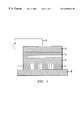
- FIG. 1 shows the cross section of an embodiment of the invention as a four layer polarized organic light emitting diode.
- FIG. 2 shows the cross section of an embodiment of the invention as a five layer polarized organic light emitting diode, which includes a conducting polymer layered between the alignment material and the photoactive material.
- FIG. 3 shows the cross section of an embodiment of the invention as a polarized organic photovoltaic device.
- FIG. 4 shows the chemical structures of some of the species used in the polarized organic photonics devices.
- FIG. 5 shows the polarized micrographs of a photoactive polymer cast on a substrate with a friction transferred PTFE alignment layer.
- FIG. 6 shows the parallel and perpendicular absorption spectra of a PPV12 film cast on a substrate with a friction transferred PTFE alignment layer.
- FIG. 7 shows the parallel and perpendicular photoluminescence spectra of a PPV12 film cast on a substrate with a friction transferred PTFE alignment layer.
- FIG. 8 shows the parallel and perpendicular electroluminescence spectra of one embodiment of the invention as an LED using 1G6-OMe as the photoactive material.
- the polarized organic devices described herein and the methods for their fabrication are based on forming a sequence of stacked layers of selected materials in a selected order.
- the thickness of each of the layers depends on the material and the intended device application.
- layers as used herein are understood to be quasi 2-dimensional objects such that they essentially have only two surfaces.
- layer B is formed or deposited on an outer surface of layer A
- only one outer surface of layer B remains exposed.
- layer C is subsequently formed on an outer surface of layer B it is understood that the configuration described is a sequence of three layers stacked in the unique order A-B-C.
- any layer unless specified otherwise, may consist of a sequence of sublayers.
- the process for fabricating a polarized organic photonics device comprises the steps of preparing a sequence of stacked layers by first forming an alignment layer on top of a first conducting layer or conducting substrate.
- the first conducting layer or substrate serves as a first electrode in the photonics device.
- the alignment layer provides an alignment template and direction to orient photoactive materials, which are subsequently deposited onto the previous layer or layers.
- a second conducting layer (which serves as a second electrode in the photonics device), thereby forming a polarized organic photonics device.
- the alignment layer provides for the alignment of subsequently deposited organic and polymeric layers, a prerequisite for a polarized device.
- the alignment layer typically a thin layer of an insulating, electron transporting, or hole transporting material, is deposited by a friction transfer method.
- the alignment material is poly(tetrafluoroethylene) (PTFE).
- the alignment layer may be other materials as well.
- Another suitable material is poly(phenylene) (PPP).
- PPP poly(phenylene)
- UHMWPE ultra-high molecular weight polyethylene
- F. Motamedi 32 J. Polymer Sci: B 453 (1994), incorporated herein by reference teach that polyethylene, the thermotropic liquid-crystalline Vectra®, and fluorinated ethylene-propylene copolymers are
- the friction transfer method used to prepared the alignment layer on the electrically conductive substrate is achieved by pressing a solid structure (pellet, bar, ingot, rod, stick or the like) of the alignment material against the substrate and drawing the solid alignment material across the structure in a selected direction under a pressure sufficient to transfer a thin layer of the alignment material onto the substrate.
- the selected direction of the friction transfer typically, though not necessarily, a single linear axis, provides an orientation direction for the alignment of subsequent layers.
- the friction transfer method is described more fully in U.S. Pat. No. 5,180,460, which is incorporated herein by reference.
- the substrate may either be heated or unheated to optimize the transfer and control the thickness of the transferred alignment film.
- Oriented friction transfer alignment structures facilitate nucleation and formation of highly oriented structures deposited thereon.
- U.S. Pat No. 5,772,755 incorporated herein by reference, teaches that a thin film of PTFE also may be prepared for use as an alignment layer by spreading a powder or dispersion across the substrate. These deposition methods of U.S. Pat No. 5,772,755 is included under the scope and meaning of the friction transfer method.
- the thickness of the alignment layer should be sufficient to impart alignment on subsequent layers. It should also be thin enough such that it is not completely insulating. Preferably, the average thickness of the alignment layer should be less than 10 nm. More preferably, the average thickness should be less that 1 nm.
- an electrically conducting polymer may be deposited onto the alignment layer. This step may be carried out at elevated temperatures to enhance the uniformity of the deposited layer. Alternately, the conducting polymer may be deposited at room temperature, or below, to yield preferential deposition in regions with less PTFE, or other alignment material. In this latter method, the addition of the conducting polymer yields a more uniform base for subsequently deposited layers.
- This step of depositing an electrically conducting polymer may be carried out using a gaseous-phase, aerosol, casting or melt method. It is preferable that the conducting polymer is poly(3,4-ethylenedioxythiophene) (PEDOT), polyaniline, polypyrrole, or conducting polythiophene.
- a photoactive material is deposited.
- the photoactive material itself may a multi-layer structure.
- the photoactive layer consists of a photoactive material layered between a hole transporting material on one side and/or an electron transporting material on the second side.
- the photoactive material may also be a blend of or sequence of stacked layers of one or more photoactive materials.
- the photoactive layer may comprise a hole transporting (p-type) layer and an electron transporting (n-type) layer having a photoactive material incorporated into one or both layers.
- the photoactive material may be an organic or polymeric material. If the photoactive material is an organic molecule, it may be 1,2-bis(di-4-tolylaminophenyl)cyclohexane (TAPC) or 3,4,9,10-perylenetetracarboxylic dianhydride (PTCDA). If the photoactive material is a polymer, it may be a rigid, linear conjugated polymer.
- TAPC 1,2-bis(di-4-tolylaminophenyl)cyclohexane
- PTCDA 3,4,9,10-perylenetetracarboxylic dianhydride
- the photoactive material is a polymer, it may be a rigid, linear conjugated polymer.
- the photoactive material may be a polymer such as poly ⁇ [2,5-bis(n-dodecan-1-yloxy)-1,4-phenylene]vinylene-1,4-phenylene vinylene ⁇ (PPV12), poly ⁇ 2-methoxy-5-[3′,4′,5′-tris(n-dodecan-1-yloxy)benzyloxy]-1,4-phenylene ⁇ vinylene-1,4-phenylene vinylene ⁇ (1G12-OMe), poly ⁇ 2-methoxy-5-[3′,4′,5′-tris(n-hexan-1-yloxy)benzyloxy]-1,4-phenylene ⁇ vinylene-1,4-phenylene vinylene ⁇ (1G6-OMe), or poly ⁇ 2,5-bis[3′,4′,5′-tris(n-dodecan-1-yloxy)benzyloxy]-1,4-phenylene ⁇ vinylene-1,4-phenylene vinylene ⁇ (PPV
- the photoactive material may also be blended or layered with other materials to enhance or modify the optical and or electronic responses of the photonics device.
- fullerenes are a suitable additive to the photoactive material to enhance device response.
- fullerene means a carbon allotrope, which is also called carbon cluster.
- the fullerenes hitherto known are those having such molecular-formulas as C 60 , C 70 , C 76 , C 78 , C 82 , C 84 , C 90 , C 96 , etc.
- a mixture can be used which comprises two or more of these fullerenes.
- C 60 and C 70 preferred for use in the present invention are C 60 and C 70 , and particularly preferred is C 60 .
- Substituted fullerenes, fullerene derivatives, polymers comprising fullerenes or substituted fullerenes may also be blended or layered with the photoactive material.
- the deposition of the photoactive material may also be carried out at elevated temperature, to enhance uniformity and to further increase the alignment of the photoactive material to the alignment layer or bi-layer.
- This step may be carried out by contacting the photoactive material with the alignment layer (or bi-layer structure) with the photoactive material in a gaseous phase or as an aerosol, from a solution by a casting method, or as a solid by melt processing.
- the substrate is heated to a temperature above the boiling point of the solution used to cast the photoactive material onto the alignment layer (or bi-layer structure). This method is valuable in that it induces alignment of the photoactive material beginning from the substrate.
- the first and/or the second electrically conductive layers both of which serve as electrodes for the device, be transparent or semi-transparent to light.
- Possible conductive layers include indium tin oxide (ITO) or a conducting polymer, both of which may be optically transparent.
- the electrically conducting layer may also be a metal film, such as gold, aluminum, silver, or copper. If this layer is to be transparent, or substantially transparent, then the metallic layer may be relatively thin and still conduct electricity but also transmit light.
- One of the conducting layers may also be reflective, or semi-reflective, or selectively reflective, to, for example, direct unabsorbed light back into the active material, in the case of a photovoltaic device, or to direct emitted light out of the device into a preferred direction, in the case of a LED.
- the first electrically conductive layer is preferably formed on a substrate.
- This substrate may be optically transparent or semi-transparent to allow light to enter and/or leave the device.
- the substrate may be any shape. It may preferably be substantially planer, concave, or convex.
- the shape of the substrate, as well as its other material and optical properties, may be chosen and or designed to control the transmission and/or reflection ought into and/or out of the device by, for example, focussing, collimating, or diverging light.
- the conducting layers may be conformal with a surface of any arbitrary shape.
- the two electrodes have different work functions.
- the polarized organic photonics device may be designed to perform a number of functions. Among these functions, the device, for example, may be used as a polarized organic light emitting diode.
- FIG. 1 depicts one embodiment of the current invention in the form of a four layer LED.
- Substrate 10 serves as a support for a transparent electrically conductive electrode 11 made from ITO, which is coated with a friction transferred PTFE layer 12 , and onto which a layer of photoactive material 13 has been formed, an aluminum electrode 14 is the final layer in the stacked sequence and the device can be operated as an LED by applying an electrical signal across the circuit 15 connecting the two electrodes.
- FIG. 2 depicts one of the preferred embodiments of the invention in the form of a five layer LED.
- Substrate 20 serves as a support for a transparent electrically conductive electrode 21 made from ITO, which is coated with a friction transferred PTFE layer 22 , and onto which a conducting polymer layer 26 has been formed, and onto which a layer of photoactive material 23 has been formed, an aluminum electrode 24 is the final layer in the stacked sequence and the device can be operated as an LED by applying an electrical signal across the circuit 25 connecting the two electrodes.
- the polarized organic photonics device may also be designed to be a polarized photovoltaic device.
- FIG. 3 depicts one of the preferred embodiments of the invention where the device is a photovoltaic device.
- Light enters the device through an optically transparent substrate 30 which serves as a support for an optically transparent electrically conductive electrode 31 , onto which a friction transferred PTFE layer 32 has been formed, and onto which a layer of the photoactive material 33 is formed, and with the final layer in the stacked sequence is a second electrically conductive electrode 34 .
- a photo-induced electrical signal may be measured or an electrical load may be driven in the circuit 35 , which connects the two electrodes.
- FIG. 4 depicts the chemical structures of some of the chemical species that may be used in the polarized organic photonics devices of this invention.
- This example demonstrates the process of preparing polarized organic photoactive layers by casting on a friction transferred PTFE treated substrate.
- PTFE was rubbed on glass substrates.
- Photoactive polymer layers approximately 100 nm thick, were then deposited on the PTFE treated substrates by casting from solution.
- Polarized micrographs of PPV12 and 1G6-OMe, the structures of which are shown in FIG. 4, prepared according to this method are shown in FIG. 5 .
- the PTFE component is sufficiently thin and colorless and does not contribute significantly to light intensity through crossed polarizers. When the film is rotated and the PTFE friction direction is oriented parallel to the polarizer, almost complete extinction of the transmitted light is observed. This indicates that most polymers are oriented parallel to the PTFE friction transfer direction.
- FIGS. 6 and 7 show the parallel and perpendicular absorption and photoluminescence spectra from thin films cast from PPV12/chloroform solution on PTFE rubbed glass substrates. Intensities of absorption and emission along the friction transfer direction (parallel) are much higher than those obtained from the perpendicular direction.
- the ratios between the parallel and perpendicular are 4.1 to 1 and 6.7 to 1 for absorption and emission, respectively. Energy transfer in the film after photoexcitation probably causes the difference between the two ratios.
- each polymer film was approximately 100 nm. From Table I, it is apparent that fewer and smaller side chains leads to greater anisotropy, which is indicative of a greater degree of photoactive material alignment and orientation the film gets. The highest anisotropy was obtained in the thin film of PPV12.
- This example demonstrates how the process of preparing polarized photoactive layers is used to yield a polarized organic light-emitting device.
- ITO indium-tin-oxide
- a thin film of photoactive material 1G6-OMe was prepared by casting solutions of the photoactive material in chloroform or tetrahydrofuran onto the preheated (100° C.) substrate. The synthesis of this photoactive material, and others used herein, has been reported elsewhere.
- the film thickness of the active material was approximately 100 nm, as measured by a profilometer with 1 nm resolution and confirmed with optical absorption measurements.
- the multi-layer structure was dried in a vacuum oven at 60° C. for 24 hours. Finally, 100-130 nm thick aluminum electrodes were vacuum evaporated (at 10 ⁇ 6 Torr) onto the active layer.
- the structure of this device is shown schematically in FIG. 1 .
- FIG. 8 shows the electroluminescence (EL) spectra of this device.
- the sequence of layers is: ITO/PTFE/1G6-OMe/Al.
- the EL measurement was made in the ambient environment and at room temperature. The measurement was taken in sequence such that the EL measurement from parallel direction was taken after the measurement from the perpendicular direction.
- the lineshape of the EL spectrum is identical to both the photoluminescence (PL) spectrum and a non-aligned, unpolarized LED with layers in the sequence of ITO/1G6-OMe/Al, indicating that the PL and EL are from the same species.
- An anisotropy (ie. ratio intensity parallel to perpendicular) of 2.6 in EL was achieved with the aligned, polarized photonics device of this example.
- This example demonstrates the relative enhancement of the preferred embodiment that includes a layer of conducting polymer interposed between the alignment layer and the photoactive layer.
- This example further demonstrates that, as unique from all prior art, friction transfer alignment layers can induce alignment in organic and polymeric layers even when an additional organic layer is interposed between them.
- devices with a PEDOT layer interposed between the PTFE and the photoactive material have superior performance in terms of stability, quantum efficiency, and brightness.
- a device of this structure is shown schematically in FIG. 2 .
- ITO/PTFE/PEDOT/1G6-OMe/Al have comparable quantum efficiency (2.0 ⁇ 10 ⁇ 3 ) to unoriented LED devices without PTFE treatment such as ITO/PEDOT/1G6-OMe/Al (quantum efficiency 2.2 ⁇ 10 ⁇ 3 ).
- the polarized organic photonics device is a polarized organic photovoltaic device.
- the active materials here can be a single component, blends or multilayers, and can be aligned with the help of PTFE layer.
- the light absorbing active materials sandwiched between two conducting electrodes, at least one of which should be transparent or semitransparent (for light to pass).
- the absorbed light energy when the light is shined on the device (through the transparent electrode), the absorbed light energy (absorbed by active materials) first results in the highly efficient generation of excitons (electron-hole pair) in the bulk film of the photoactive material.
- this device is more sensitive than others since all chromophores can take part in absorbing light, in contrast to a device with randomly orientated chromophores where only light parallel to dipole moment of chromophores gets absorbed. Furthermore, the device described in this example can detect the polarization of the light.
- the materials for the first electrodes in this device may be ITO, Au, Ni, and other semitransparent or transparent conducting materials.
- Materials suitable for the second electrode include any conducting materials, and need not necessarily be transparent. For applications such as photovoltaic devices, it is preferred that the two electrodes have different work functions.
- Materials for photoactive layer may be, for a single layer, a PPV12-C 60 blend.
- a suitable sequence of layers and materials is, for example: ITO/PTFE/p-type materials (e.g. PPV12)/n-type materials (e.g. PTCDA)/Al. In this configuration, because the work function of ITO is greater than that of Al electrons will go to the Al electrode and holes will go to the ITO electrode.
- the configuration could be: ITO/PTFE/PPV12-n-type materials blend (e.g. C 60 )/p-type materials (e.g. TAPC)/Au.
- ITO/PTFE/PPV12-n-type materials blend e.g. C 60
- p-type materials e.g. TAPC
Abstract
Description
| TABLE I |
| Dichroic absorption and photo luminescence ratios for |
| polymers cast on PTFE treated substrates |
| Dichroic Ratio |
| Polymer | Absorption | Photoluminescence | ||
| PPV12 | 4.1 | 6.7 | ||
| 1G6-OMe | 3 | 4.2 | ||
| 1G12-S | 2.7 | 3.3 | ||
| 2G6-S | 1.6 | 1.7 | ||
Claims (31)
Priority Applications (4)
| Application Number | Priority Date | Filing Date | Title |
|---|---|---|---|
| US09/394,524 US6489044B1 (en) | 1999-09-01 | 1999-09-01 | Process for fabricating polarized organic photonics devices, and resultant articles |
| EP00307376A EP1081774A2 (en) | 1999-09-01 | 2000-08-29 | Process for fabricating polarized organic photonics devices |
| JP2000270155A JP2001143873A (en) | 1999-09-01 | 2000-09-06 | Method for manufacturing polarized organic photonics device |
| US10/266,454 US6579564B2 (en) | 1999-09-01 | 2002-10-08 | Process for fabricating polarized organic photonics devices |
Applications Claiming Priority (1)
| Application Number | Priority Date | Filing Date | Title |
|---|---|---|---|
| US09/394,524 US6489044B1 (en) | 1999-09-01 | 1999-09-01 | Process for fabricating polarized organic photonics devices, and resultant articles |
Related Child Applications (1)
| Application Number | Title | Priority Date | Filing Date |
|---|---|---|---|
| US10/266,454 Division US6579564B2 (en) | 1999-09-01 | 2002-10-08 | Process for fabricating polarized organic photonics devices |
Publications (1)
| Publication Number | Publication Date |
|---|---|
| US6489044B1 true US6489044B1 (en) | 2002-12-03 |
Family
ID=23559316
Family Applications (2)
| Application Number | Title | Priority Date | Filing Date |
|---|---|---|---|
| US09/394,524 Expired - Lifetime US6489044B1 (en) | 1999-09-01 | 1999-09-01 | Process for fabricating polarized organic photonics devices, and resultant articles |
| US10/266,454 Expired - Fee Related US6579564B2 (en) | 1999-09-01 | 2002-10-08 | Process for fabricating polarized organic photonics devices |
Family Applications After (1)
| Application Number | Title | Priority Date | Filing Date |
|---|---|---|---|
| US10/266,454 Expired - Fee Related US6579564B2 (en) | 1999-09-01 | 2002-10-08 | Process for fabricating polarized organic photonics devices |
Country Status (3)
| Country | Link |
|---|---|
| US (2) | US6489044B1 (en) |
| EP (1) | EP1081774A2 (en) |
| JP (1) | JP2001143873A (en) |
Cited By (25)
| Publication number | Priority date | Publication date | Assignee | Title |
|---|---|---|---|---|
| US20030119936A1 (en) * | 2001-06-29 | 2003-06-26 | O'neill Mary | Light emitting polymer |
| US6628068B1 (en) * | 1998-12-12 | 2003-09-30 | Sharp Kabushiki Kaisha | Luminescent device and a liquid crystal device incorporating a luminescent device |
| US20040170861A1 (en) * | 2003-02-28 | 2004-09-02 | Eastman Kodak Company | Organic light emitting diodes for production of polarized light |
| US20040183972A1 (en) * | 2001-04-20 | 2004-09-23 | Bell Gareth Paul | Optical retarder |
| US20040224083A1 (en) * | 2000-11-28 | 2004-11-11 | Wu Long Hai | Method for fabricating electroluminescence element |
| US20040245917A1 (en) * | 2003-04-23 | 2004-12-09 | Zheng-Hong Lu | Light-emitting devices with an embedded charge injection electrode |
| US6830831B2 (en) * | 2001-06-29 | 2004-12-14 | University Of Hull | Light emitter for a display |
| US20050096404A1 (en) * | 2001-06-29 | 2005-05-05 | University Of Hull | Light emitting polymer |
| US20060099448A1 (en) * | 2003-04-28 | 2006-05-11 | Zheng-Hong Lu | Top light-emitting devices with fullerene layer |
| US20060103951A1 (en) * | 2002-03-17 | 2006-05-18 | Bell Gareth P | Method to control point spread function of an image |
| US20060152147A1 (en) * | 2005-01-07 | 2006-07-13 | Lee Tae-Woo | Electroluminescent device and method for preparing the same |
| US20060284574A1 (en) * | 2003-05-21 | 2006-12-21 | Emslie James S | Backlighting system for display screen |
| US20060290594A1 (en) * | 2002-07-15 | 2006-12-28 | Engel Gabriel D | Multilayer video screen |
| US20070062577A1 (en) * | 2005-03-21 | 2007-03-22 | Markus Koppe | Polymer photovoltaic cell |
| US20070107776A1 (en) * | 2002-01-25 | 2007-05-17 | Konarka Technologies, Inc., A Delaware Corporation | Photovoltaic powered multimedia greeting cards and smart cards |
| US20070243786A1 (en) * | 2002-08-09 | 2007-10-18 | Semiconductor Energy Laboratory Co. Ltd. | Organic electroluminescent device |
| US20080152842A1 (en) * | 2000-11-17 | 2008-06-26 | Pure Depth Limited | Altering surfaces of display screens |
| US20090021153A1 (en) * | 2005-01-07 | 2009-01-22 | Lee Tae-Woo | Electroluminescent device and method for preparing the same |
| US20090051623A1 (en) * | 2007-08-22 | 2009-02-26 | Paul Gareth P | Method and system for determining a position for an interstital diffuser for use in a multi-layer display |
| US7498739B1 (en) * | 2004-09-30 | 2009-03-03 | Rockwell Collins, Inc. | Polarized light source using an organic liquid crystal |
| US20110176090A1 (en) * | 2005-12-30 | 2011-07-21 | Lg Display Co., Ltd. | Display device and fabrication method thereof |
| US8146277B2 (en) | 2002-09-20 | 2012-04-03 | Puredepth Limited | Multi-view display |
| US20160172612A1 (en) * | 2006-08-07 | 2016-06-16 | Wake Forest University | Composite organic materials and applications thereof |
| US20170148853A1 (en) * | 2015-11-24 | 2017-05-25 | General Electric Company | Processes for fabricating organic x-ray detectors, related organic x-ray detectors and systems |
| CN108230908A (en) * | 2018-01-03 | 2018-06-29 | 京东方科技集团股份有限公司 | A kind of display panel and display device |
Families Citing this family (27)
| Publication number | Priority date | Publication date | Assignee | Title |
|---|---|---|---|---|
| US6485884B2 (en) * | 2001-04-27 | 2002-11-26 | 3M Innovative Properties Company | Method for patterning oriented materials for organic electronic displays and devices |
| EP1405355B1 (en) * | 2001-07-09 | 2020-02-26 | Flexenable Limited | Progressive aligned deposition |
| NZ514500A (en) | 2001-10-11 | 2004-06-25 | Deep Video Imaging Ltd | A multiplane visual display unit with a transparent emissive layer disposed between two display planes |
| US6649436B2 (en) * | 2002-02-11 | 2003-11-18 | Eastman Kodak Company | Using organic materials in making an organic light-emitting device |
| JP3926180B2 (en) | 2002-03-26 | 2007-06-06 | シャープ株式会社 | ORGANIC EL LIGHT EMITTING ELEMENT AND LIQUID CRYSTAL DISPLAY DEVICE USING THE SAME |
| US20040224182A1 (en) * | 2003-01-07 | 2004-11-11 | Lazarev Pavel I. | Backlight polar organic light-emitting device |
| EP1447860A1 (en) * | 2003-02-17 | 2004-08-18 | Rijksuniversiteit Groningen | Organic material photodiode |
| GB2403023A (en) * | 2003-06-20 | 2004-12-22 | Sharp Kk | Organic light emitting device |
| US7291223B2 (en) * | 2003-09-24 | 2007-11-06 | Nitto Denko Corporation | Epitaxial organic layered structure and method for making |
| CN1947276A (en) * | 2004-04-27 | 2007-04-11 | 皇家飞利浦电子股份有限公司 | Method of forming an organic semiconducting device by a melt technique |
| US20060003487A1 (en) * | 2004-06-30 | 2006-01-05 | Intel Corporation | Low power consumption OLED material for display applications |
| US20060105200A1 (en) * | 2004-11-17 | 2006-05-18 | Dmytro Poplavskyy | Organic electroluminescent device |
| CN101416227B (en) * | 2005-12-06 | 2011-02-23 | 杜比实验室特许公司 | Modular electronic displays |
| WO2008048349A2 (en) * | 2006-03-06 | 2008-04-24 | National Institute Of Aerospace Associates | Depositing nanometer-sized metal particles onto substrates |
| ATE515807T1 (en) * | 2006-05-01 | 2011-07-15 | Univ Wake Forest | ORGANIC OPTOELECTRONIC DEVICES AND APPLICATIONS THEREOF |
| AU2007248170B2 (en) | 2006-05-01 | 2012-08-16 | Arrowhead Center, Inc. | Fiber photovoltaic devices and applications thereof |
| DE102006043216A1 (en) * | 2006-06-02 | 2007-12-06 | Inoviscoat Gmbh | Composite material for oral administration of medicinal agent, has layers containing active ingredient, ceramic nanoparticles, silver salt, or nanoparticulate carbon modification material |
| US20080149178A1 (en) * | 2006-06-27 | 2008-06-26 | Marisol Reyes-Reyes | Composite organic materials and applications thereof |
| US8790773B2 (en) * | 2007-07-20 | 2014-07-29 | The United States Of America As Represented By The Administrator Of The National Aeronautics And Space Administration | Tailorable dielectric material with complex permittivity characteristics |
| WO2009045341A1 (en) * | 2007-09-28 | 2009-04-09 | The Johns Hopkins University | Megahertz organic/polymer diodes and methods related thereto |
| WO2009059303A2 (en) * | 2007-11-01 | 2009-05-07 | Wake Forest University | Lateral organic optoelectronic devices and applications thereof |
| JP5207229B2 (en) * | 2007-11-12 | 2013-06-12 | Jnc株式会社 | Polarized organic electroluminescent device |
| CN102929047B (en) | 2008-02-28 | 2015-05-20 | 住友化学株式会社 | Transparent thin-film electrode |
| CN102460714A (en) * | 2009-06-03 | 2012-05-16 | 密执安州立大学董事会 | Structural templating for organic electronic devices having an organic film with long range order |
| CN103764777B (en) | 2011-08-25 | 2016-08-17 | Lg化学株式会社 | Contact adhesive |
| JP5991507B2 (en) * | 2012-02-28 | 2016-09-14 | 国立大学法人北陸先端科学技術大学院大学 | Method for producing photoelectric conversion device, photoelectric conversion device and production device for photoelectric conversion device |
| JP2015529344A (en) * | 2012-08-27 | 2015-10-05 | エルジー・ケム・リミテッド | Polarizer |
Citations (8)
| Publication number | Priority date | Publication date | Assignee | Title |
|---|---|---|---|---|
| US5180470A (en) | 1989-06-05 | 1993-01-19 | The Regents Of The University Of California | Deposition of highly-oriented PTFE films and uses therefor |
| US5350459A (en) | 1992-05-01 | 1994-09-27 | Ricoh Company, Ltd. | Organic photovoltaic element |
| US5454880A (en) | 1992-08-17 | 1995-10-03 | Regents Of The University Of California | Conjugated polymer-acceptor heterojunctions; diodes, photodiodes, and photovoltaic cells |
| US5546889A (en) | 1993-10-06 | 1996-08-20 | Matsushita Electric Industrial Co., Ltd. | Method of manufacturing organic oriented film and method of manufacturing electronic device |
| US5669708A (en) * | 1993-02-10 | 1997-09-23 | Nikon Corporation | Optical element, production method of optical element, optical system, and optical apparatus |
| US5677545A (en) | 1994-09-12 | 1997-10-14 | Motorola | Organic light emitting diodes with molecular alignment and method of fabrication |
| US5772755A (en) * | 1996-08-01 | 1998-06-30 | W. L. Gore & Associates, Inc. | Oriented crystalline materials |
| US5919579A (en) | 1994-08-08 | 1999-07-06 | Hoechst Aktiengesellschaft | Organic electroluminescent device |
Family Cites Families (2)
| Publication number | Priority date | Publication date | Assignee | Title |
|---|---|---|---|---|
| US4672265A (en) * | 1984-07-31 | 1987-06-09 | Canon Kabushiki Kaisha | Electroluminescent device |
| US6399221B1 (en) * | 1996-06-25 | 2002-06-04 | Northwestern University | Organic light-emitting diodes and methods for assembly and emission control |
-
1999
- 1999-09-01 US US09/394,524 patent/US6489044B1/en not_active Expired - Lifetime
-
2000
- 2000-08-29 EP EP00307376A patent/EP1081774A2/en not_active Withdrawn
- 2000-09-06 JP JP2000270155A patent/JP2001143873A/en active Pending
-
2002
- 2002-10-08 US US10/266,454 patent/US6579564B2/en not_active Expired - Fee Related
Patent Citations (8)
| Publication number | Priority date | Publication date | Assignee | Title |
|---|---|---|---|---|
| US5180470A (en) | 1989-06-05 | 1993-01-19 | The Regents Of The University Of California | Deposition of highly-oriented PTFE films and uses therefor |
| US5350459A (en) | 1992-05-01 | 1994-09-27 | Ricoh Company, Ltd. | Organic photovoltaic element |
| US5454880A (en) | 1992-08-17 | 1995-10-03 | Regents Of The University Of California | Conjugated polymer-acceptor heterojunctions; diodes, photodiodes, and photovoltaic cells |
| US5669708A (en) * | 1993-02-10 | 1997-09-23 | Nikon Corporation | Optical element, production method of optical element, optical system, and optical apparatus |
| US5546889A (en) | 1993-10-06 | 1996-08-20 | Matsushita Electric Industrial Co., Ltd. | Method of manufacturing organic oriented film and method of manufacturing electronic device |
| US5919579A (en) | 1994-08-08 | 1999-07-06 | Hoechst Aktiengesellschaft | Organic electroluminescent device |
| US5677545A (en) | 1994-09-12 | 1997-10-14 | Motorola | Organic light emitting diodes with molecular alignment and method of fabrication |
| US5772755A (en) * | 1996-08-01 | 1998-06-30 | W. L. Gore & Associates, Inc. | Oriented crystalline materials |
Non-Patent Citations (8)
| Title |
|---|
| Gill et al, Highly Oriented Thin Films of a Substituted Oligo(para-phenylenevinylene) on Friction-transferred PTFE Substrates, Adv. Mater. 1997, 9, No. 4 No Month. * |
| Hamaguchi et al, Polarized electroluminescence from rubbing-aligned poly(2,5-dinonyloxy-1,4-phenylenevinylene) films, Appl. Phys. Lett. 67(23), Dec. 4, 1995.* * |
| M. Era et al., "Polarized electroluminescence from oriented p-sexiphenyl vacuum-deposited film," 67(17) Appl.Phys.Lett 2436 (1995). No Month. |
| P. Dyreklev et al., "Polarized Electroluminescence from an Oriented Substituted Polythiophene in a Light Emitting Diode," 7(1) Adv.Mater. 43 (1995). No Month. |
| Tanigaki et al., "Oriented thin films of conjugated polymers: polysilanes and polyphenylenes," 331 Thin Solid Films 229 (1998). No Month. |
| Ueda et al., "Structure and crystal growth of low molecular weight polyethylene vapor-deposited on polymer friction-transferred layers," 331 Thin Solid Films 216 (1998). No Month. |
| V. Cimorva et al, "Polarized Light Emission from LEDs Prepared by the Langmui-Blodgett Technique," 8(2) Adv.Mater. 146 (1996). No Month. |
| Wittmann et al., "Highly oriented thin films of poly(tetrafluorothylene) as a substrate for oriented growth of materials," 352 Nature 414 (1991). No Month. |
Cited By (51)
| Publication number | Priority date | Publication date | Assignee | Title |
|---|---|---|---|---|
| US6628068B1 (en) * | 1998-12-12 | 2003-09-30 | Sharp Kabushiki Kaisha | Luminescent device and a liquid crystal device incorporating a luminescent device |
| US8154691B2 (en) | 2000-11-17 | 2012-04-10 | Pure Depth Limited | Altering surfaces of display screens |
| US20080152842A1 (en) * | 2000-11-17 | 2008-06-26 | Pure Depth Limited | Altering surfaces of display screens |
| US20040224083A1 (en) * | 2000-11-28 | 2004-11-11 | Wu Long Hai | Method for fabricating electroluminescence element |
| US7742124B2 (en) | 2001-04-20 | 2010-06-22 | Puredepth Limited | Optical retarder |
| US20040183972A1 (en) * | 2001-04-20 | 2004-09-23 | Bell Gareth Paul | Optical retarder |
| US20100201921A1 (en) * | 2001-04-20 | 2010-08-12 | Pure Depth Limited | Optical retarder |
| US7199167B2 (en) | 2001-06-29 | 2007-04-03 | University Of Hull | Light emitting polymer |
| US20070194277A1 (en) * | 2001-06-29 | 2007-08-23 | O'neill Mary | Light emitting polymer |
| US20050040396A1 (en) * | 2001-06-29 | 2005-02-24 | University Of Hull | Light emitter for a display |
| US6867243B2 (en) | 2001-06-29 | 2005-03-15 | University Of Hull | Light emitting polymer |
| US20050096404A1 (en) * | 2001-06-29 | 2005-05-05 | University Of Hull | Light emitting polymer |
| US20030119936A1 (en) * | 2001-06-29 | 2003-06-26 | O'neill Mary | Light emitting polymer |
| US20050004251A1 (en) * | 2001-06-29 | 2005-01-06 | University Of Hull | Light emitting polymer |
| US7265163B2 (en) | 2001-06-29 | 2007-09-04 | University Of Hull | Light emitting polymer |
| US20050004252A1 (en) * | 2001-06-29 | 2005-01-06 | University Of Hull | Light emitting polymer |
| US7081307B2 (en) | 2001-06-29 | 2006-07-25 | University Of Hull | Light emitter for a display |
| US6830831B2 (en) * | 2001-06-29 | 2004-12-14 | University Of Hull | Light emitter for a display |
| US7166239B2 (en) | 2001-06-29 | 2007-01-23 | University Of Hull | Light emitting polymer |
| US20070107776A1 (en) * | 2002-01-25 | 2007-05-17 | Konarka Technologies, Inc., A Delaware Corporation | Photovoltaic powered multimedia greeting cards and smart cards |
| US20110188134A1 (en) * | 2002-03-17 | 2011-08-04 | Pure Depth Limited | Method and system for controlling point spread of an object |
| US7742239B2 (en) | 2002-03-17 | 2010-06-22 | Puredepth Limited | Method to control point spread function of an image |
| US20060103951A1 (en) * | 2002-03-17 | 2006-05-18 | Bell Gareth P | Method to control point spread function of an image |
| US20060290594A1 (en) * | 2002-07-15 | 2006-12-28 | Engel Gabriel D | Multilayer video screen |
| US9137525B2 (en) | 2002-07-15 | 2015-09-15 | Pure Depth Limited | Multilayer video screen |
| US20070243786A1 (en) * | 2002-08-09 | 2007-10-18 | Semiconductor Energy Laboratory Co. Ltd. | Organic electroluminescent device |
| US9650245B2 (en) | 2002-08-09 | 2017-05-16 | Semiconductor Energy Laboratory Co., Ltd. | Organic electroluminescent device |
| US8146277B2 (en) | 2002-09-20 | 2012-04-03 | Puredepth Limited | Multi-view display |
| US7037599B2 (en) | 2003-02-28 | 2006-05-02 | Eastman Kodak Company | Organic light emitting diodes for production of polarized light |
| US20040170861A1 (en) * | 2003-02-28 | 2004-09-02 | Eastman Kodak Company | Organic light emitting diodes for production of polarized light |
| US20040245917A1 (en) * | 2003-04-23 | 2004-12-09 | Zheng-Hong Lu | Light-emitting devices with an embedded charge injection electrode |
| US20060099448A1 (en) * | 2003-04-28 | 2006-05-11 | Zheng-Hong Lu | Top light-emitting devices with fullerene layer |
| US20060284574A1 (en) * | 2003-05-21 | 2006-12-21 | Emslie James S | Backlighting system for display screen |
| US7439683B2 (en) | 2003-05-21 | 2008-10-21 | Pure Depth Limited | Backlighting system for display screen |
| US7498739B1 (en) * | 2004-09-30 | 2009-03-03 | Rockwell Collins, Inc. | Polarized light source using an organic liquid crystal |
| US8134291B2 (en) | 2005-01-07 | 2012-03-13 | Samsung Mobile Display Co., Ltd. | Electroluminescent device and method for preparing the same |
| US20090021153A1 (en) * | 2005-01-07 | 2009-01-22 | Lee Tae-Woo | Electroluminescent device and method for preparing the same |
| US20060152147A1 (en) * | 2005-01-07 | 2006-07-13 | Lee Tae-Woo | Electroluminescent device and method for preparing the same |
| US7825326B2 (en) | 2005-03-21 | 2010-11-02 | Konarka Technologies, Inc. | Polymer photovoltaic cell |
| WO2006101814A3 (en) * | 2005-03-21 | 2009-04-09 | Konarka Technologies Inc | Polymer photovoltaic cell |
| US20070062577A1 (en) * | 2005-03-21 | 2007-03-22 | Markus Koppe | Polymer photovoltaic cell |
| US8107037B2 (en) * | 2005-12-30 | 2012-01-31 | Lg Display Co., Ltd. | Display device and fabrication method thereof |
| KR101221352B1 (en) | 2005-12-30 | 2013-01-11 | 엘지디스플레이 주식회사 | Display device and and method for fabricating the same |
| US20110176090A1 (en) * | 2005-12-30 | 2011-07-21 | Lg Display Co., Ltd. | Display device and fabrication method thereof |
| US20160172612A1 (en) * | 2006-08-07 | 2016-06-16 | Wake Forest University | Composite organic materials and applications thereof |
| US8416150B2 (en) | 2007-08-22 | 2013-04-09 | Igt | Method and system for determining a position for an interstital diffuser for use in a multi-layer display |
| US20090051623A1 (en) * | 2007-08-22 | 2009-02-26 | Paul Gareth P | Method and system for determining a position for an interstital diffuser for use in a multi-layer display |
| US20170148853A1 (en) * | 2015-11-24 | 2017-05-25 | General Electric Company | Processes for fabricating organic x-ray detectors, related organic x-ray detectors and systems |
| US9929216B2 (en) * | 2015-11-24 | 2018-03-27 | General Electric Company | Processes for fabricating organic X-ray detectors, related organic X-ray detectors and systems |
| CN108230908A (en) * | 2018-01-03 | 2018-06-29 | 京东方科技集团股份有限公司 | A kind of display panel and display device |
| US20190207135A1 (en) * | 2018-01-03 | 2019-07-04 | Boe Technology Group Co., Ltd. | Display panel and display device |
Also Published As
| Publication number | Publication date |
|---|---|
| JP2001143873A (en) | 2001-05-25 |
| US20030035979A1 (en) | 2003-02-20 |
| US6579564B2 (en) | 2003-06-17 |
| EP1081774A2 (en) | 2001-03-07 |
Similar Documents
| Publication | Publication Date | Title |
|---|---|---|
| US6489044B1 (en) | Process for fabricating polarized organic photonics devices, and resultant articles | |
| Salaneck et al. | Conjugated Polymer and Molecular Interfaces: Science and Technology for Photonic and Optoelectronic Application | |
| Bliznyuk et al. | Electrical and photoinduced degradation of polyfluorene based films and light-emitting devices | |
| Brütting | Introduction to the physics of organic semiconductors | |
| JP4594832B2 (en) | Photocell and manufacturing method thereof | |
| KR100696903B1 (en) | Polyimide layer comprising functional material, device employing the same and method of manufacturing same device | |
| Ouali et al. | Oligo (phenylenevinylene)/fullerene photovoltaic cells: Influence of morphology | |
| Lee et al. | Highly efficient red-emitting hybrid polymer light-emitting diodes via Forster resonance energy transfer based on homogeneous polymer blends with the same polyfluorene backbone | |
| US20140087501A1 (en) | Doped graphene transparent conductive electrode | |
| Chen et al. | Polarized electroluminescence from aligned chromophores by the friction transfer method | |
| US20140087500A1 (en) | Transparent conductive electrode stack containing carbon-containing material | |
| Seo et al. | Organic light-emitting field-effect transistors based upon pentacene and perylene | |
| Gadisa et al. | Red and near infrared polarized light emissions from polyfluorene copolymer based light emitting diodes | |
| Halls et al. | Organic photovoltaic devices | |
| Park et al. | Investigations of the polymer alignment, the nonradiative resonant energy transfer, and the photovoltaic response of poly (3-hexylthiophene)/TiO2 hybrid solar cells | |
| Lee et al. | Application of a novel fullerene-containing copolymer to electroluminescent devices | |
| Thelakkat et al. | Materials Screening and Combinatorial Development of Thin Film Multilayer Electro‐Optical Devices | |
| Takamatsu et al. | Cellulose-Templated Stable Foldable Oriented Films with Polarized RGB Luminescence | |
| WO2004075314A1 (en) | Discotic liquid crystal based electronic device using interdigit structure electrode | |
| Tsai et al. | Electroluminescence from Spontaneously Generated Single-Vesicle Aggregates Using Solution-Processed Small Organic Molecules | |
| Tuffy | Porphyrin Materials for Organic Light Emitting Diodes: A Route to Phosphorescent Emission | |
| JP4088471B2 (en) | Organic light emitting device and method for manufacturing the same | |
| Nabha-Barnea et al. | Microscopic investigation of degradation processes in a polyfluorene blend by near-field scanning optical microscopy | |
| Lin et al. | Electronic process in organic solids | |
| Engmann et al. | Magnetic Field Sensor Based on a OLED/Organic Photodetector Stack |
Legal Events
| Date | Code | Title | Description |
|---|---|---|---|
| AS | Assignment |
Owner name: LUCENT TECHNOLOGIES INC., NEW JERSEY Free format text: ASSIGNMENT OF ASSIGNORS INTEREST;ASSIGNORS:CHEN, XIAOCHUN LINDA;BAO, ZHENAN;REEL/FRAME:010463/0646 Effective date: 19990910 |
|
| STCF | Information on status: patent grant |
Free format text: PATENTED CASE |
|
| FPAY | Fee payment |
Year of fee payment: 4 |
|
| FEPP | Fee payment procedure |
Free format text: PAYOR NUMBER ASSIGNED (ORIGINAL EVENT CODE: ASPN); ENTITY STATUS OF PATENT OWNER: LARGE ENTITY |
|
| FPAY | Fee payment |
Year of fee payment: 8 |
|
| FPAY | Fee payment |
Year of fee payment: 12 |
|
| AS | Assignment |
Owner name: PROVENANCE ASSET GROUP LLC, CONNECTICUT Free format text: ASSIGNMENT OF ASSIGNORS INTEREST;ASSIGNORS:NOKIA TECHNOLOGIES OY;NOKIA SOLUTIONS AND NETWORKS BV;ALCATEL LUCENT SAS;REEL/FRAME:043877/0001 Effective date: 20170912 Owner name: NOKIA USA INC., CALIFORNIA Free format text: SECURITY INTEREST;ASSIGNORS:PROVENANCE ASSET GROUP HOLDINGS, LLC;PROVENANCE ASSET GROUP LLC;REEL/FRAME:043879/0001 Effective date: 20170913 Owner name: CORTLAND CAPITAL MARKET SERVICES, LLC, ILLINOIS Free format text: SECURITY INTEREST;ASSIGNORS:PROVENANCE ASSET GROUP HOLDINGS, LLC;PROVENANCE ASSET GROUP, LLC;REEL/FRAME:043967/0001 Effective date: 20170913 |
|
| AS | Assignment |
Owner name: ALCATEL-LUCENT USA INC., NEW JERSEY Free format text: CHANGE OF NAME;ASSIGNOR:LUCENT TECHNOLOGIES INC.;REEL/FRAME:049887/0613 Effective date: 20081101 |
|
| AS | Assignment |
Owner name: NOKIA US HOLDINGS INC., NEW JERSEY Free format text: ASSIGNMENT AND ASSUMPTION AGREEMENT;ASSIGNOR:NOKIA USA INC.;REEL/FRAME:048370/0682 Effective date: 20181220 |
|
| AS | Assignment |
Owner name: PROVENANCE ASSET GROUP LLC, CONNECTICUT Free format text: RELEASE BY SECURED PARTY;ASSIGNOR:CORTLAND CAPITAL MARKETS SERVICES LLC;REEL/FRAME:058983/0104 Effective date: 20211101 Owner name: PROVENANCE ASSET GROUP HOLDINGS LLC, CONNECTICUT Free format text: RELEASE BY SECURED PARTY;ASSIGNOR:CORTLAND CAPITAL MARKETS SERVICES LLC;REEL/FRAME:058983/0104 Effective date: 20211101 Owner name: PROVENANCE ASSET GROUP LLC, CONNECTICUT Free format text: RELEASE BY SECURED PARTY;ASSIGNOR:NOKIA US HOLDINGS INC.;REEL/FRAME:058363/0723 Effective date: 20211129 Owner name: PROVENANCE ASSET GROUP HOLDINGS LLC, CONNECTICUT Free format text: RELEASE BY SECURED PARTY;ASSIGNOR:NOKIA US HOLDINGS INC.;REEL/FRAME:058363/0723 Effective date: 20211129 |
|
| AS | Assignment |
Owner name: RPX CORPORATION, CALIFORNIA Free format text: ASSIGNMENT OF ASSIGNORS INTEREST;ASSIGNOR:PROVENANCE ASSET GROUP LLC;REEL/FRAME:059352/0001 Effective date: 20211129 |