US6489489B2 - Organic electroluminescent device - Google Patents
Organic electroluminescent device Download PDFInfo
- Publication number
- US6489489B2 US6489489B2 US09/778,816 US77881601A US6489489B2 US 6489489 B2 US6489489 B2 US 6489489B2 US 77881601 A US77881601 A US 77881601A US 6489489 B2 US6489489 B2 US 6489489B2
- Authority
- US
- United States
- Prior art keywords
- group
- organic
- carbon atoms
- bonded
- host compound
- Prior art date
- Legal status (The legal status is an assumption and is not a legal conclusion. Google has not performed a legal analysis and makes no representation as to the accuracy of the status listed.)
- Expired - Lifetime
Links
- 0 */C([Y])=C/C.*/C([Y])=C\C.CC.CC.CC.CC.CC.CC.CC.CC.CC.CC.CC.CC.CC.CC.CC.CC.CC.CC.CC.CC.CC.CC.CC.CC.c1ccccc1.c1ccccc1.c1ccccc1.c1ccccc1.c1ccccc1 Chemical compound */C([Y])=C/C.*/C([Y])=C\C.CC.CC.CC.CC.CC.CC.CC.CC.CC.CC.CC.CC.CC.CC.CC.CC.CC.CC.CC.CC.CC.CC.CC.CC.c1ccccc1.c1ccccc1.c1ccccc1.c1ccccc1.c1ccccc1 0.000 description 26
- XSDWSTPREXOGKG-UHFFFAOYSA-N C(=C(c1ccccc1)c1cccc2ccccc12)c1ccc(-c2ccc(-c3ccc(-c4ccc(C=C(c5ccccc5)c5cccc6ccccc56)cc4)cc3)cc2)cc1.C(=C(c1ccccc1)c1ccccc1)c1ccc(-c2ccc(-c3ccc(-c4ccc(C=C(c5ccccc5)c5ccccc5)cc4)c(-c4ccccc4)c3)cc2-c2ccccc2)cc1.C(=C(c1ccccc1)c1ccccc1)c1ccc(-c2ccc(-c3ccc(-c4ccc(C=C(c5ccccc5)c5ccccc5)cc4)cc3)cc2)cc1.C(=C(c1ccccc1)c1ccccc1)c1ccc(-c2ccc(-c3ccc(-c4ccc(C=C(c5ccccc5)c5ccccc5)cc4)cc3)cc2)cc1.C(=C(c1ccccc1)c1ccccc1)c1ccc2c(c1)CCc1cc3c(cc1-2)CCc1cc2c(cc1-3)CCc1cc(C=C(c3ccccc3)c3ccccc3)ccc1-2.CBr.CBr.CC#N.CN(c1ccccc1)c1ccccc1.CN(c1ccccc1)c1ccccc1.COC.COC.Cc1ccccc1.Cc1ccccc1.Cc1ccccc1.Cc1ccccc1.Cc1ccccc1.Cc1ccccc1.Cc1ccccc1.Cc1ccccc1.Cc1ccccc1.Cc1ccccc1.Clc1c(Cl)c(-c2c(Cl)c(Cl)c(-c3c(Cl)c(Cl)c(-c4c(Cl)c(Cl)c(C=C(c5ccccc5)c5cc6ccc7cccc8ccc(c5)c6c78)c(Cl)c4Cl)c(Cl)c3Cl)c(Cl)c2Cl)c(Cl)c(Cl)c1C=C(c1ccccc1)c1cc2ccc3cccc4ccc(c1)c2c34.[C-]#[N+]C Chemical compound C(=C(c1ccccc1)c1cccc2ccccc12)c1ccc(-c2ccc(-c3ccc(-c4ccc(C=C(c5ccccc5)c5cccc6ccccc56)cc4)cc3)cc2)cc1.C(=C(c1ccccc1)c1ccccc1)c1ccc(-c2ccc(-c3ccc(-c4ccc(C=C(c5ccccc5)c5ccccc5)cc4)c(-c4ccccc4)c3)cc2-c2ccccc2)cc1.C(=C(c1ccccc1)c1ccccc1)c1ccc(-c2ccc(-c3ccc(-c4ccc(C=C(c5ccccc5)c5ccccc5)cc4)cc3)cc2)cc1.C(=C(c1ccccc1)c1ccccc1)c1ccc(-c2ccc(-c3ccc(-c4ccc(C=C(c5ccccc5)c5ccccc5)cc4)cc3)cc2)cc1.C(=C(c1ccccc1)c1ccccc1)c1ccc2c(c1)CCc1cc3c(cc1-2)CCc1cc2c(cc1-3)CCc1cc(C=C(c3ccccc3)c3ccccc3)ccc1-2.CBr.CBr.CC#N.CN(c1ccccc1)c1ccccc1.CN(c1ccccc1)c1ccccc1.COC.COC.Cc1ccccc1.Cc1ccccc1.Cc1ccccc1.Cc1ccccc1.Cc1ccccc1.Cc1ccccc1.Cc1ccccc1.Cc1ccccc1.Cc1ccccc1.Cc1ccccc1.Clc1c(Cl)c(-c2c(Cl)c(Cl)c(-c3c(Cl)c(Cl)c(-c4c(Cl)c(Cl)c(C=C(c5ccccc5)c5cc6ccc7cccc8ccc(c5)c6c78)c(Cl)c4Cl)c(Cl)c3Cl)c(Cl)c2Cl)c(Cl)c(Cl)c1C=C(c1ccccc1)c1cc2ccc3cccc4ccc(c1)c2c34.[C-]#[N+]C XSDWSTPREXOGKG-UHFFFAOYSA-N 0.000 description 2
- SIWRHDJIJQDJNO-UHFFFAOYSA-N C(=C(c1ccccc1)c1ccccc1)c1c2ccccc2c(-c2c3ccccc3c(-c3c4ccccc4c(-c4c5ccccc5c(C=C(c5ccccc5)c5ccccc5)c5ccccc45)c4ccccc34)c3ccccc23)c2ccccc12.C(=C(c1ccccc1)c1ccccc1)c1ccc(-c2c3ccccc3c(-c3c4ccccc4c(-c4ccc(C=C(c5ccccc5)c5ccccc5)cc4)c4ccccc34)c3ccccc23)cc1.C(=C(c1ccccc1)c1ccccc1)c1ccc(-c2ccc(-c3ccc(-c4ccc(C=C(c5ccccc5)c5ccccc5)c5ccccc45)c4ccccc34)c3ccccc23)c2ccccc12.C(=C(c1ccccc1)c1ccccc1)c1ccc(-c2ccc(-c3ccc(-c4ccc(C=C(c5ccccc5)c5ccccc5)c5ccccc45)cc3)cc2)c2ccccc12.C(=C(c1ccccc1)c1ccccc1)c1ccc(-c2ccc(-c3ccc(-c4ccc(C=C(c5ccccc5)c5ccccc5)cc4)c4ccccc34)c3ccccc23)cc1.C(=C(c1ccccc1)c1ccccc1)c1ccc(-c2ccc3c(c2)-c2cc(-c4ccc(C=C(c5ccccc5)c5ccccc5)cc4)ccc2-3)cc1.C(=C(c1ccccc1)c1ccccc1)c1ccc(-c2ccc3c(ccc4cc(-c5ccc(C=C(c6ccccc6)c6ccccc6)cc5)ccc43)c2)cc1 Chemical compound C(=C(c1ccccc1)c1ccccc1)c1c2ccccc2c(-c2c3ccccc3c(-c3c4ccccc4c(-c4c5ccccc5c(C=C(c5ccccc5)c5ccccc5)c5ccccc45)c4ccccc34)c3ccccc23)c2ccccc12.C(=C(c1ccccc1)c1ccccc1)c1ccc(-c2c3ccccc3c(-c3c4ccccc4c(-c4ccc(C=C(c5ccccc5)c5ccccc5)cc4)c4ccccc34)c3ccccc23)cc1.C(=C(c1ccccc1)c1ccccc1)c1ccc(-c2ccc(-c3ccc(-c4ccc(C=C(c5ccccc5)c5ccccc5)c5ccccc45)c4ccccc34)c3ccccc23)c2ccccc12.C(=C(c1ccccc1)c1ccccc1)c1ccc(-c2ccc(-c3ccc(-c4ccc(C=C(c5ccccc5)c5ccccc5)c5ccccc45)cc3)cc2)c2ccccc12.C(=C(c1ccccc1)c1ccccc1)c1ccc(-c2ccc(-c3ccc(-c4ccc(C=C(c5ccccc5)c5ccccc5)cc4)c4ccccc34)c3ccccc23)cc1.C(=C(c1ccccc1)c1ccccc1)c1ccc(-c2ccc3c(c2)-c2cc(-c4ccc(C=C(c5ccccc5)c5ccccc5)cc4)ccc2-3)cc1.C(=C(c1ccccc1)c1ccccc1)c1ccc(-c2ccc3c(ccc4cc(-c5ccc(C=C(c6ccccc6)c6ccccc6)cc5)ccc43)c2)cc1 SIWRHDJIJQDJNO-UHFFFAOYSA-N 0.000 description 2
- IRHQFMMQLQCQMU-UHFFFAOYSA-N C(=C(c1ccccc1)c1ccccc1)c1ccc(-c2c3ccccc3c(-c3c4ccccc4c(-c4c5ccccc5c(-c5ccc(C=C(c6ccccc6)c6ccccc6)cc5)c5ccccc45)c4ccccc34)c3ccccc23)cc1.C(=C(c1ccccc1)c1ccccc1)c1ccc(-c2ccc(-c3c4ccccc4c(-c4ccc(-c5ccc(C=C(c6ccccc6)c6ccccc6)cc5)c5ccccc45)c4ccccc34)c3ccccc23)cc1.C(=C(c1ccccc1)c1ccccc1)c1ccc(-c2ccc3c(c2)CCc2cc4c(cc2-3)CCc2cc(-c3ccc(C=C(c5ccccc5)c5ccccc5)cc3)ccc2-4)cc1.CC(c1ccccc1)(c1ccccc1)c1cc(-c2ccc(-c3ccc4c(c3)C(c3ccccc3)(c3ccccc3)c3cc(C=C(c5ccccc5)c5ccccc5)ccc3-4)cc2)ccc1-c1ccc(C=C(c2ccccc2)c2ccccc2)cc1.CN(c1ccccc1)c1cc(-c2ccc(-c3ccc4c(c3)N(c3ccccc3)c3cc(C=C(c5ccc(-c6ccccc6)cc5)c5ccc(-c6ccccc6)cc5)ccc3-4)cc2)ccc1-c1ccc(C=C(c2ccc(-c3ccccc3)cc2)c2ccc(-c3ccccc3)cc2)cc1.COc1cc(-c2ccc(-c3c4ccccc4c(C=C(c4ccccc4)c4ccccc4)c4ccccc34)cc2)c(OC)cc1-c1ccc(-c2c3ccccc3c(C=C(c3ccccc3)c3ccccc3)c3ccccc23)cc1.Cc1cc(-c2ccc(-c3ccc(C=C(c4ccccc4)c4ccccc4)c4ccccc34)cc2)c(C)cc1-c1ccc(-c2ccc(C=C(c3ccccc3)c3ccccc3)c3ccccc23)cc1.[HH].[HH] Chemical compound C(=C(c1ccccc1)c1ccccc1)c1ccc(-c2c3ccccc3c(-c3c4ccccc4c(-c4c5ccccc5c(-c5ccc(C=C(c6ccccc6)c6ccccc6)cc5)c5ccccc45)c4ccccc34)c3ccccc23)cc1.C(=C(c1ccccc1)c1ccccc1)c1ccc(-c2ccc(-c3c4ccccc4c(-c4ccc(-c5ccc(C=C(c6ccccc6)c6ccccc6)cc5)c5ccccc45)c4ccccc34)c3ccccc23)cc1.C(=C(c1ccccc1)c1ccccc1)c1ccc(-c2ccc3c(c2)CCc2cc4c(cc2-3)CCc2cc(-c3ccc(C=C(c5ccccc5)c5ccccc5)cc3)ccc2-4)cc1.CC(c1ccccc1)(c1ccccc1)c1cc(-c2ccc(-c3ccc4c(c3)C(c3ccccc3)(c3ccccc3)c3cc(C=C(c5ccccc5)c5ccccc5)ccc3-4)cc2)ccc1-c1ccc(C=C(c2ccccc2)c2ccccc2)cc1.CN(c1ccccc1)c1cc(-c2ccc(-c3ccc4c(c3)N(c3ccccc3)c3cc(C=C(c5ccc(-c6ccccc6)cc5)c5ccc(-c6ccccc6)cc5)ccc3-4)cc2)ccc1-c1ccc(C=C(c2ccc(-c3ccccc3)cc2)c2ccc(-c3ccccc3)cc2)cc1.COc1cc(-c2ccc(-c3c4ccccc4c(C=C(c4ccccc4)c4ccccc4)c4ccccc34)cc2)c(OC)cc1-c1ccc(-c2c3ccccc3c(C=C(c3ccccc3)c3ccccc3)c3ccccc23)cc1.Cc1cc(-c2ccc(-c3ccc(C=C(c4ccccc4)c4ccccc4)c4ccccc34)cc2)c(C)cc1-c1ccc(-c2ccc(C=C(c3ccccc3)c3ccccc3)c3ccccc23)cc1.[HH].[HH] IRHQFMMQLQCQMU-UHFFFAOYSA-N 0.000 description 2
- ADVNQGTVLQRBCH-UHFFFAOYSA-N C(=C(c1ccccc1)c1ccccc1)c1c2c(c(-c3ccc(-c4c5c(c(C=C(c6ccccc6)c6ccccc6)c6c4CCCC6)CCCC5)c4c3CC(c3ccccc3)C(c3ccccc3)C4)c3c1CCCC3)CCCC2.C(=C(c1ccccc1)c1ccccc1)c1c2ccccc2c(-c2c3ccccc3c(-c3c4ccccc4c(C=C(c4ccccc4)c4ccccc4)c4ccccc34)c3ccccc23)c2ccccc12.C(=C(c1ccccc1)c1ccccc1)c1c2ccccc2c(-c2ccc(-c3c4ccccc4c(C=C(c4ccccc4)c4ccccc4)c4ccccc34)cc2)c2ccccc12.C(=C(c1ccccc1)c1ccccc1)c1ccc(-c2c3ccccc3c(-c3ccc(C=C(c4ccccc4)c4ccccc4)cc3)c3ccccc23)cc1.C(=C(c1ccccc1)c1ccccc1)c1ccc(-c2ccc(-c3ccc(C=C(c4ccccc4)c4ccccc4)c4ccccc34)c3ccccc23)c2ccccc12.C(=C(c1ccccc1)c1ccccc1)c1ccc(-c2ccc(-c3ccc(C=C(c4ccccc4)c4ccccc4)c4ccccc34)cc2)c2ccccc12.C(=C(c1ccccc1)c1ccccc1)c1ccc(-c2ccc(-c3ccc(C=C(c4ccccc4)c4ccccc4)cc3)c3ccccc23)cc1 Chemical compound C(=C(c1ccccc1)c1ccccc1)c1c2c(c(-c3ccc(-c4c5c(c(C=C(c6ccccc6)c6ccccc6)c6c4CCCC6)CCCC5)c4c3CC(c3ccccc3)C(c3ccccc3)C4)c3c1CCCC3)CCCC2.C(=C(c1ccccc1)c1ccccc1)c1c2ccccc2c(-c2c3ccccc3c(-c3c4ccccc4c(C=C(c4ccccc4)c4ccccc4)c4ccccc34)c3ccccc23)c2ccccc12.C(=C(c1ccccc1)c1ccccc1)c1c2ccccc2c(-c2ccc(-c3c4ccccc4c(C=C(c4ccccc4)c4ccccc4)c4ccccc34)cc2)c2ccccc12.C(=C(c1ccccc1)c1ccccc1)c1ccc(-c2c3ccccc3c(-c3ccc(C=C(c4ccccc4)c4ccccc4)cc3)c3ccccc23)cc1.C(=C(c1ccccc1)c1ccccc1)c1ccc(-c2ccc(-c3ccc(C=C(c4ccccc4)c4ccccc4)c4ccccc34)c3ccccc23)c2ccccc12.C(=C(c1ccccc1)c1ccccc1)c1ccc(-c2ccc(-c3ccc(C=C(c4ccccc4)c4ccccc4)c4ccccc34)cc2)c2ccccc12.C(=C(c1ccccc1)c1ccccc1)c1ccc(-c2ccc(-c3ccc(C=C(c4ccccc4)c4ccccc4)cc3)c3ccccc23)cc1 ADVNQGTVLQRBCH-UHFFFAOYSA-N 0.000 description 1
- YCXWVHNDUIGCEI-UHFFFAOYSA-N C(=C(c1ccccc1)c1ccccc1)c1c2c(c(-c3ccc(-c4c5c(c(C=C(c6ccccc6)c6ccccc6)c6c4CCCC6)CCCC5)c4c3CC(c3ccccc3)C(c3ccccc3)C4)c3c1CCCC3)CCCC2.C(=C(c1ccccc1)c1ccccc1)c1c2ccccc2c(-c2c3ccccc3c(-c3c4ccccc4c(C=C(c4ccccc4)c4ccccc4)c4ccccc34)c3ccccc23)c2ccccc12.C(=C(c1ccccc1)c1ccccc1)c1c2ccccc2c(-c2ccc(-c3c4ccccc4c(C=C(c4ccccc4)c4ccccc4)c4ccccc34)cc2)c2ccccc12.C(=C(c1ccccc1)c1ccccc1)c1ccc(-c2c3ccccc3c(-c3ccc(C=C(c4ccccc4)c4ccccc4)cc3)c3ccccc23)cc1.C(=C(c1ccccc1)c1ccccc1)c1ccc(-c2ccc(-c3ccc(C=C(c4ccccc4)c4ccccc4)c4ccccc34)c3ccccc23)c2ccccc12.C(=C(c1ccccc1)c1ccccc1)c1ccc(-c2ccc(-c3ccc(C=C(c4ccccc4)c4ccccc4)c4ccccc34)cc2)c2ccccc12.C(=C(c1ccccc1)c1ccccc1)c1ccc(-c2ccc(-c3ccc(C=C(c4ccccc4)c4ccccc4)cc3)c3ccccc23)cc1.[HH].[HH].[HH].[HH].[HH] Chemical compound C(=C(c1ccccc1)c1ccccc1)c1c2c(c(-c3ccc(-c4c5c(c(C=C(c6ccccc6)c6ccccc6)c6c4CCCC6)CCCC5)c4c3CC(c3ccccc3)C(c3ccccc3)C4)c3c1CCCC3)CCCC2.C(=C(c1ccccc1)c1ccccc1)c1c2ccccc2c(-c2c3ccccc3c(-c3c4ccccc4c(C=C(c4ccccc4)c4ccccc4)c4ccccc34)c3ccccc23)c2ccccc12.C(=C(c1ccccc1)c1ccccc1)c1c2ccccc2c(-c2ccc(-c3c4ccccc4c(C=C(c4ccccc4)c4ccccc4)c4ccccc34)cc2)c2ccccc12.C(=C(c1ccccc1)c1ccccc1)c1ccc(-c2c3ccccc3c(-c3ccc(C=C(c4ccccc4)c4ccccc4)cc3)c3ccccc23)cc1.C(=C(c1ccccc1)c1ccccc1)c1ccc(-c2ccc(-c3ccc(C=C(c4ccccc4)c4ccccc4)c4ccccc34)c3ccccc23)c2ccccc12.C(=C(c1ccccc1)c1ccccc1)c1ccc(-c2ccc(-c3ccc(C=C(c4ccccc4)c4ccccc4)c4ccccc34)cc2)c2ccccc12.C(=C(c1ccccc1)c1ccccc1)c1ccc(-c2ccc(-c3ccc(C=C(c4ccccc4)c4ccccc4)cc3)c3ccccc23)cc1.[HH].[HH].[HH].[HH].[HH] YCXWVHNDUIGCEI-UHFFFAOYSA-N 0.000 description 1
- KSBURPIJGKNEQZ-UHFFFAOYSA-N C(=C(c1ccccc1)c1ccccc1)c1ccc(-c2cc3c4c(c2)CCc2cc(-c5ccc(C=C(c6ccccc6)c6ccccc6)cc5)cc(c2-4)CC3)cc1.C(=C(c1ccccc1)c1ccccc1)c1ccc(-c2cc3ccc4cc(-c5ccc(C=C(c6ccccc6)c6ccccc6)cc5)cc5ccc(c2)c3c45)cc1.C(=C(c1ccccc1)c1ccccc1)c1ccc(-c2ccc3c(c2)C(c2ccccc2)(c2ccccc2)c2cc(-c4ccc(C=C(c5ccccc5)c5ccccc5)cc4)ccc2-3)cc1.C(=C(c1ccccc1)c1ccccc1)c1ccc(-c2ccc3c(c2)N(c2ccccc2)c2cc(-c4ccc(C=C(c5ccccc5)c5ccccc5)cc4)ccc2-3)cc1.C/C1=C(\C)c2cc(-c3ccc(C=C(c4ccccc4)c4ccccc4)cc3)ccc2-c2ccc(-c3ccc(C=C(c4ccccc4)c4ccccc4)cc3)cc21.Cc1cc(-c2ccc3c(c2)N(Cc2ccccc2)c2cc(-c4ccc(C=C(c5ccccc5)c5ccccc5)c(C)c4)ccc2-3)ccc1C=C(c1ccccc1)c1ccccc1 Chemical compound C(=C(c1ccccc1)c1ccccc1)c1ccc(-c2cc3c4c(c2)CCc2cc(-c5ccc(C=C(c6ccccc6)c6ccccc6)cc5)cc(c2-4)CC3)cc1.C(=C(c1ccccc1)c1ccccc1)c1ccc(-c2cc3ccc4cc(-c5ccc(C=C(c6ccccc6)c6ccccc6)cc5)cc5ccc(c2)c3c45)cc1.C(=C(c1ccccc1)c1ccccc1)c1ccc(-c2ccc3c(c2)C(c2ccccc2)(c2ccccc2)c2cc(-c4ccc(C=C(c5ccccc5)c5ccccc5)cc4)ccc2-3)cc1.C(=C(c1ccccc1)c1ccccc1)c1ccc(-c2ccc3c(c2)N(c2ccccc2)c2cc(-c4ccc(C=C(c5ccccc5)c5ccccc5)cc4)ccc2-3)cc1.C/C1=C(\C)c2cc(-c3ccc(C=C(c4ccccc4)c4ccccc4)cc3)ccc2-c2ccc(-c3ccc(C=C(c4ccccc4)c4ccccc4)cc3)cc21.Cc1cc(-c2ccc3c(c2)N(Cc2ccccc2)c2cc(-c4ccc(C=C(c5ccccc5)c5ccccc5)c(C)c4)ccc2-3)ccc1C=C(c1ccccc1)c1ccccc1 KSBURPIJGKNEQZ-UHFFFAOYSA-N 0.000 description 1
- ATSKRLMORMKPLI-UHFFFAOYSA-N C(=C(c1ccccc1)c1ccccc1)c1ccc(-c2cc3c4c(c2)CCc2cc(-c5ccc(C=C(c6ccccc6)c6ccccc6)cc5)cc(c2-4)CC3)cc1.C(=C(c1ccccc1)c1ccccc1)c1ccc(-c2cc3ccc4cc(-c5ccc(C=C(c6ccccc6)c6ccccc6)cc5)cc5ccc(c2)c3c45)cc1.C(=C(c1ccccc1)c1ccccc1)c1ccc(-c2ccc3c(c2)C(c2ccccc2)(c2ccccc2)c2cc(-c4ccc(C=C(c5ccccc5)c5ccccc5)cc4)ccc2-3)cc1.C(=C(c1ccccc1)c1ccccc1)c1ccc(-c2ccc3c(c2)N(c2ccccc2)c2cc(-c4ccc(C=C(c5ccccc5)c5ccccc5)cc4)ccc2-3)cc1.C/C1=C(\C)c2cc(-c3ccc(C=C(c4ccccc4)c4ccccc4)cc3)ccc2-c2ccc(-c3ccc(C=C(c4ccccc4)c4ccccc4)cc3)cc21.Cc1cc(-c2ccc3c(c2)N(Cc2ccccc2)c2cc(-c4ccc(C=C(c5ccccc5)c5ccccc5)c(C)c4)ccc2-3)ccc1C=C(c1ccccc1)c1ccccc1.[HH].[HH] Chemical compound C(=C(c1ccccc1)c1ccccc1)c1ccc(-c2cc3c4c(c2)CCc2cc(-c5ccc(C=C(c6ccccc6)c6ccccc6)cc5)cc(c2-4)CC3)cc1.C(=C(c1ccccc1)c1ccccc1)c1ccc(-c2cc3ccc4cc(-c5ccc(C=C(c6ccccc6)c6ccccc6)cc5)cc5ccc(c2)c3c45)cc1.C(=C(c1ccccc1)c1ccccc1)c1ccc(-c2ccc3c(c2)C(c2ccccc2)(c2ccccc2)c2cc(-c4ccc(C=C(c5ccccc5)c5ccccc5)cc4)ccc2-3)cc1.C(=C(c1ccccc1)c1ccccc1)c1ccc(-c2ccc3c(c2)N(c2ccccc2)c2cc(-c4ccc(C=C(c5ccccc5)c5ccccc5)cc4)ccc2-3)cc1.C/C1=C(\C)c2cc(-c3ccc(C=C(c4ccccc4)c4ccccc4)cc3)ccc2-c2ccc(-c3ccc(C=C(c4ccccc4)c4ccccc4)cc3)cc21.Cc1cc(-c2ccc3c(c2)N(Cc2ccccc2)c2cc(-c4ccc(C=C(c5ccccc5)c5ccccc5)c(C)c4)ccc2-3)ccc1C=C(c1ccccc1)c1ccccc1.[HH].[HH] ATSKRLMORMKPLI-UHFFFAOYSA-N 0.000 description 1
- XLXUUKHKXQACKV-UDSAUWFTSA-N C(=C(c1ccccc1)c1ccccc1)c1ccc(-c2ccc(-c3ccc(-c4ccc(-c5ccc(C=C(c6ccccc6)c6ccccc6)cc5)c5ccccc45)c4ccccc34)c3ccccc23)cc1.C(=C(c1ccccc1)c1ccccc1)c1ccc(-c2ccc(-c3ccc(-c4ccc(-c5ccc(C=C(c6ccccc6)c6ccccc6)cc5)cc4)cc3)cc2)cc1.C(=C(c1ccccc1)c1ccccc1)c1ccc(-c2ccc3c(c2)Oc2cc(-c4ccc(C=C(c5ccccc5)c5ccccc5)c5c4COC5)ccc2-3)c2c1COC2.CC(c1ccccc1)(c1ccccc1)c1cc(-c2ccc3c(c2)C(c2ccccc2)(c2ccccc2)c2cc(C=C(c4ccccc4)c4ccccc4)ccc2-3)ccc1-c1ccc(C=C(c2ccccc2)c2ccccc2)cc1.COc1cc(-c2ccc3c(ccc4cc(-c5cc(C)c(/C=C(\c6ccccc6)c6ccc(N(c7ccccc7)c7ccccc7)cc6)cc5OC)ccc43)c2)c(OC)cc1/C=C(\c1ccccc1)c1ccc(N(c2ccccc2)c2ccccc2)cc1.Cc1cc(-c2ccc(-c3ccc(-c4ccc(C=C(c5ccccc5)c5ccccc5)cc4)c(C)c3)cc2)ccc1-c1ccc(C=C(c2ccccc2)c2ccccc2)cc1.O.[C-]#[N+]c1ccc(/C(=C/c2ccc(-c3cc4c5c(c3)Cc3cc(-c6ccc(/C=C(/c7ccc(C#N)cc7)c7cccc8ccccc78)cc6)cc(c3-5)C4)cc2)c2cccc3ccccc23)cc1 Chemical compound C(=C(c1ccccc1)c1ccccc1)c1ccc(-c2ccc(-c3ccc(-c4ccc(-c5ccc(C=C(c6ccccc6)c6ccccc6)cc5)c5ccccc45)c4ccccc34)c3ccccc23)cc1.C(=C(c1ccccc1)c1ccccc1)c1ccc(-c2ccc(-c3ccc(-c4ccc(-c5ccc(C=C(c6ccccc6)c6ccccc6)cc5)cc4)cc3)cc2)cc1.C(=C(c1ccccc1)c1ccccc1)c1ccc(-c2ccc3c(c2)Oc2cc(-c4ccc(C=C(c5ccccc5)c5ccccc5)c5c4COC5)ccc2-3)c2c1COC2.CC(c1ccccc1)(c1ccccc1)c1cc(-c2ccc3c(c2)C(c2ccccc2)(c2ccccc2)c2cc(C=C(c4ccccc4)c4ccccc4)ccc2-3)ccc1-c1ccc(C=C(c2ccccc2)c2ccccc2)cc1.COc1cc(-c2ccc3c(ccc4cc(-c5cc(C)c(/C=C(\c6ccccc6)c6ccc(N(c7ccccc7)c7ccccc7)cc6)cc5OC)ccc43)c2)c(OC)cc1/C=C(\c1ccccc1)c1ccc(N(c2ccccc2)c2ccccc2)cc1.Cc1cc(-c2ccc(-c3ccc(-c4ccc(C=C(c5ccccc5)c5ccccc5)cc4)c(C)c3)cc2)ccc1-c1ccc(C=C(c2ccccc2)c2ccccc2)cc1.O.[C-]#[N+]c1ccc(/C(=C/c2ccc(-c3cc4c5c(c3)Cc3cc(-c6ccc(/C=C(/c7ccc(C#N)cc7)c7cccc8ccccc78)cc6)cc(c3-5)C4)cc2)c2cccc3ccccc23)cc1 XLXUUKHKXQACKV-UDSAUWFTSA-N 0.000 description 1
- LJIFGJHEADEGJX-UHFFFAOYSA-N C(=C(c1ccccc1)c1ccccc1)c1ccc(-c2ccc(-c3ccc(-c4ccc(-c5ccc(C=C(c6ccccc6)c6ccccc6)cc5)c5ccccc45)c4ccccc34)c3ccccc23)cc1.C(=C(c1ccccc1)c1ccccc1)c1ccc(-c2ccc(-c3ccc(-c4ccc(-c5ccc(C=C(c6ccccc6)c6ccccc6)cc5)cc4)cc3)cc2)cc1.Cc1cc(-c2ccc(-c3ccc(-c4ccc(C=C(c5ccccc5)c5ccccc5)cc4)c(C)c3)cc2)ccc1-c1ccc(C=C(c2ccccc2)c2ccccc2)cc1 Chemical compound C(=C(c1ccccc1)c1ccccc1)c1ccc(-c2ccc(-c3ccc(-c4ccc(-c5ccc(C=C(c6ccccc6)c6ccccc6)cc5)c5ccccc45)c4ccccc34)c3ccccc23)cc1.C(=C(c1ccccc1)c1ccccc1)c1ccc(-c2ccc(-c3ccc(-c4ccc(-c5ccc(C=C(c6ccccc6)c6ccccc6)cc5)cc4)cc3)cc2)cc1.Cc1cc(-c2ccc(-c3ccc(-c4ccc(C=C(c5ccccc5)c5ccccc5)cc4)c(C)c3)cc2)ccc1-c1ccc(C=C(c2ccccc2)c2ccccc2)cc1 LJIFGJHEADEGJX-UHFFFAOYSA-N 0.000 description 1
- GJRVCYNBXFEKOJ-UHFFFAOYSA-N C(=C(c1ccccc1)c1ccccc1)c1ccc(-c2ccc(-c3ccc(-c4ccc(-c5ccc(C=C(c6ccccc6)c6ccccc6)cc5)cc4)cc3)cc2)cc1.C(=C(c1ccccc1)c1ccccc1)c1ccc(-c2ccc(-c3ccc(-c4ccc(C=C(c5ccccc5)c5ccccc5)cc4)cc3)cc2)cc1.C(=C(c1ccccc1)c1ccccc1)c1ccc(-c2ccc(-c3ccc(C=C(c4ccccc4)c4ccccc4)c4ccccc34)cc2)c2ccccc12.CC=C(c1ccccc1)c1ccccc1.CC=C(c1ccccc1)c1ccccc1.CC=C(c1ccccc1)c1ccccc1.CC=C(c1ccccc1)c1ccccc1.CC=C(c1ccccc1)c1ccccc1.CC=C(c1ccccc1)c1ccccc1.CC=C(c1ccccc1)c1ccccc1 Chemical compound C(=C(c1ccccc1)c1ccccc1)c1ccc(-c2ccc(-c3ccc(-c4ccc(-c5ccc(C=C(c6ccccc6)c6ccccc6)cc5)cc4)cc3)cc2)cc1.C(=C(c1ccccc1)c1ccccc1)c1ccc(-c2ccc(-c3ccc(-c4ccc(C=C(c5ccccc5)c5ccccc5)cc4)cc3)cc2)cc1.C(=C(c1ccccc1)c1ccccc1)c1ccc(-c2ccc(-c3ccc(C=C(c4ccccc4)c4ccccc4)c4ccccc34)cc2)c2ccccc12.CC=C(c1ccccc1)c1ccccc1.CC=C(c1ccccc1)c1ccccc1.CC=C(c1ccccc1)c1ccccc1.CC=C(c1ccccc1)c1ccccc1.CC=C(c1ccccc1)c1ccccc1.CC=C(c1ccccc1)c1ccccc1.CC=C(c1ccccc1)c1ccccc1 GJRVCYNBXFEKOJ-UHFFFAOYSA-N 0.000 description 1
- ZXPGHERNDJNEBO-UHFFFAOYSA-N C(=C(c1ccccc1)c1ccccc1)c1ccc(-c2ccc(-c3ccc(-c4ccc(C=C(c5ccccc5)c5ccccc5)cc4)cc3)cc2)cc1.C(=C(c1ccccc1)c1ccccc1)c1ccc(-c2ccc(-c3ccc(-c4ccc(C=C(c5ccccc5)c5ccccc5)cc4)cc3)cc2)cc1.C(=C(c1ccccc1)c1ccccc1)c1ccc(-c2ccc(-c3ccc(-c4ccc(C=C(c5ccccc5)c5ccccc5)cc4)cc3)cc2)cc1.C(=C(c1ccccc1)c1ccccc1)c1ccc(-c2ccc(-c3ccc(-c4ccc(C=C(c5ccccc5)c5ccccc5)cc4)cc3)cc2)cc1.C(=C(c1ccccc1)c1ccccc1)c1ccc(-c2ccc(-c3ccc(-c4ccc(C=C(c5ccccc5)c5ccccc5)cc4)cc3)cc2)cc1.C(=C1c2ccccc2Cc2ccccc21)c1ccc(-c2ccc(-c3ccc(-c4ccc(C=C5c6ccccc6Cc6ccccc65)cc4)cc3)cc2)cc1.CC.CC.CC.CC.CC.CC.CC(=Cc1ccc(-c2ccc(-c3ccc(-c4ccc(C=C(C)c5ccccc5)cc4)cc3)cc2)cc1)c1ccccc1.CC(C)(C)C.CC(C)(C)C.CC(C)(C)C.Cc1ccccc1.Cc1ccccc1.Cc1ccccc1.Cc1ccccc1.Cc1ccccc1.Cc1ccccc1.c1ccc2ccccc2c1.c1ccc2ccccc2c1 Chemical compound C(=C(c1ccccc1)c1ccccc1)c1ccc(-c2ccc(-c3ccc(-c4ccc(C=C(c5ccccc5)c5ccccc5)cc4)cc3)cc2)cc1.C(=C(c1ccccc1)c1ccccc1)c1ccc(-c2ccc(-c3ccc(-c4ccc(C=C(c5ccccc5)c5ccccc5)cc4)cc3)cc2)cc1.C(=C(c1ccccc1)c1ccccc1)c1ccc(-c2ccc(-c3ccc(-c4ccc(C=C(c5ccccc5)c5ccccc5)cc4)cc3)cc2)cc1.C(=C(c1ccccc1)c1ccccc1)c1ccc(-c2ccc(-c3ccc(-c4ccc(C=C(c5ccccc5)c5ccccc5)cc4)cc3)cc2)cc1.C(=C(c1ccccc1)c1ccccc1)c1ccc(-c2ccc(-c3ccc(-c4ccc(C=C(c5ccccc5)c5ccccc5)cc4)cc3)cc2)cc1.C(=C1c2ccccc2Cc2ccccc21)c1ccc(-c2ccc(-c3ccc(-c4ccc(C=C5c6ccccc6Cc6ccccc65)cc4)cc3)cc2)cc1.CC.CC.CC.CC.CC.CC.CC(=Cc1ccc(-c2ccc(-c3ccc(-c4ccc(C=C(C)c5ccccc5)cc4)cc3)cc2)cc1)c1ccccc1.CC(C)(C)C.CC(C)(C)C.CC(C)(C)C.Cc1ccccc1.Cc1ccccc1.Cc1ccccc1.Cc1ccccc1.Cc1ccccc1.Cc1ccccc1.c1ccc2ccccc2c1.c1ccc2ccccc2c1 ZXPGHERNDJNEBO-UHFFFAOYSA-N 0.000 description 1
- IAAWCVYPOWWFGW-UHFFFAOYSA-N C(=C(c1ccccc1)c1ccccc1)c1ccc(-c2ccc(-c3ccc(-c4ccc(C=C(c5ccccc5)c5ccccc5)cc4)cc3)cc2)cc1.C(=C(c1ccccc1)c1ccccc1)c1ccc(-c2ccc(-c3ccc(-c4ccc(C=C(c5ccccc5)c5ccccc5)cc4)cc3)cc2)cc1.C(=C(c1ccccc1)c1ccccc1)c1ccc(-c2ccc(-c3ccc(-c4ccc(C=C(c5ccccc5)c5ccccc5)cc4)cc3)cc2)cc1.C(=C(c1ccccc1)c1ccccc1)c1ccc(-c2ccc(-c3ccc(-c4ccc(C=C(c5ccccc5)c5ccccc5)cc4)cc3)cc2)cc1.C(=C(c1ccccc1)c1ccccc1)c1ccc(-c2ccc(-c3ccc(-c4ccc(C=C(c5ccccc5)c5ccccc5)cc4)cc3)cc2)cc1.C(=C1c2ccccc2Cc2ccccc21)c1ccc(-c2ccc(-c3ccc(-c4ccc(C=C5c6ccccc6Cc6ccccc65)cc4)cc3)cc2)cc1.CC.CC.CC.CC.CC.CC.CC.CC.CC(=Cc1ccc(-c2ccc(-c3ccc(-c4ccc(C=C(C)c5ccccc5)cc4)cc3)cc2)cc1)c1ccccc1.CC(C)(C)C.Cc1ccccc1.Cc1ccccc1.Cc1ccccc1.Cc1ccccc1.Cc1ccccc1.Cc1ccccc1.c1ccc2ccccc2c1.c1ccc2ccccc2c1 Chemical compound C(=C(c1ccccc1)c1ccccc1)c1ccc(-c2ccc(-c3ccc(-c4ccc(C=C(c5ccccc5)c5ccccc5)cc4)cc3)cc2)cc1.C(=C(c1ccccc1)c1ccccc1)c1ccc(-c2ccc(-c3ccc(-c4ccc(C=C(c5ccccc5)c5ccccc5)cc4)cc3)cc2)cc1.C(=C(c1ccccc1)c1ccccc1)c1ccc(-c2ccc(-c3ccc(-c4ccc(C=C(c5ccccc5)c5ccccc5)cc4)cc3)cc2)cc1.C(=C(c1ccccc1)c1ccccc1)c1ccc(-c2ccc(-c3ccc(-c4ccc(C=C(c5ccccc5)c5ccccc5)cc4)cc3)cc2)cc1.C(=C(c1ccccc1)c1ccccc1)c1ccc(-c2ccc(-c3ccc(-c4ccc(C=C(c5ccccc5)c5ccccc5)cc4)cc3)cc2)cc1.C(=C1c2ccccc2Cc2ccccc21)c1ccc(-c2ccc(-c3ccc(-c4ccc(C=C5c6ccccc6Cc6ccccc65)cc4)cc3)cc2)cc1.CC.CC.CC.CC.CC.CC.CC.CC.CC(=Cc1ccc(-c2ccc(-c3ccc(-c4ccc(C=C(C)c5ccccc5)cc4)cc3)cc2)cc1)c1ccccc1.CC(C)(C)C.Cc1ccccc1.Cc1ccccc1.Cc1ccccc1.Cc1ccccc1.Cc1ccccc1.Cc1ccccc1.c1ccc2ccccc2c1.c1ccc2ccccc2c1 IAAWCVYPOWWFGW-UHFFFAOYSA-N 0.000 description 1
- UKQBVKULFRUTKM-UHFFFAOYSA-N C(=C(c1ccccc1)c1ccccc1)c1ccc(-c2ccc3c(c2)Oc2cc(-c4ccc(C=C(c5ccccc5)c5ccccc5)c5c4COC5)ccc2-3)c2c1COC2.CC(c1ccccc1)(c1ccccc1)c1cc(-c2ccc3c(c2)C(c2ccccc2)(c2ccccc2)c2cc(C=C(c4ccccc4)c4ccccc4)ccc2-3)ccc1-c1ccc(C=C(c2ccccc2)c2ccccc2)cc1.COc1cc(-c2ccc3c(ccc4cc(-c5cc(C=O)c(C=C(c6ccccc6)c6ccc(N(c7ccccc7)c7ccccc7)cc6)cc5OC)ccc43)c2)c(OC)cc1C=C(c1ccccc1)c1ccc(N(c2ccccc2)c2ccccc2)cc1.[C-]#[N+]c1ccc(C(=Cc2ccc(-c3cc4c5c(c3)Cc3cc(-c6ccc(C=C(c7ccc(C#N)cc7)c7cccc8ccccc78)cc6)cc(c3-5)C4)cc2)c2cccc3ccccc23)cc1 Chemical compound C(=C(c1ccccc1)c1ccccc1)c1ccc(-c2ccc3c(c2)Oc2cc(-c4ccc(C=C(c5ccccc5)c5ccccc5)c5c4COC5)ccc2-3)c2c1COC2.CC(c1ccccc1)(c1ccccc1)c1cc(-c2ccc3c(c2)C(c2ccccc2)(c2ccccc2)c2cc(C=C(c4ccccc4)c4ccccc4)ccc2-3)ccc1-c1ccc(C=C(c2ccccc2)c2ccccc2)cc1.COc1cc(-c2ccc3c(ccc4cc(-c5cc(C=O)c(C=C(c6ccccc6)c6ccc(N(c7ccccc7)c7ccccc7)cc6)cc5OC)ccc43)c2)c(OC)cc1C=C(c1ccccc1)c1ccc(N(c2ccccc2)c2ccccc2)cc1.[C-]#[N+]c1ccc(C(=Cc2ccc(-c3cc4c5c(c3)Cc3cc(-c6ccc(C=C(c7ccc(C#N)cc7)c7cccc8ccccc78)cc6)cc(c3-5)C4)cc2)c2cccc3ccccc23)cc1 UKQBVKULFRUTKM-UHFFFAOYSA-N 0.000 description 1
- FGUDCVAJXDLVLU-UHFFFAOYSA-N C(CC1)CCC1N(C1CCCCC1)c(cc1)ccc1-c(cc1)ccc1N(C1CCCCC1)c(cc1)ccc1-c(cc1)ccc1N(C1CCCCC1)C1CCCCC1 Chemical compound C(CC1)CCC1N(C1CCCCC1)c(cc1)ccc1-c(cc1)ccc1N(C1CCCCC1)c(cc1)ccc1-c(cc1)ccc1N(C1CCCCC1)C1CCCCC1 FGUDCVAJXDLVLU-UHFFFAOYSA-N 0.000 description 1
- FOAQJSOHJCIBKB-UHFFFAOYSA-N C.C(=C(c1ccccc1)c1ccccc1)c1ccc(-c2ccc(-c3ccc(-c4ccc(-c5ccc(C=C(c6ccccc6)c6ccccc6)cc5)cc4)cc3)cc2)cc1.CC=C(c1ccccc1)c1ccccc1.CC=C(c1ccccc1)c1ccccc1.CC=C(c1ccccc1)c1ccccc1 Chemical compound C.C(=C(c1ccccc1)c1ccccc1)c1ccc(-c2ccc(-c3ccc(-c4ccc(-c5ccc(C=C(c6ccccc6)c6ccccc6)cc5)cc4)cc3)cc2)cc1.CC=C(c1ccccc1)c1ccccc1.CC=C(c1ccccc1)c1ccccc1.CC=C(c1ccccc1)c1ccccc1 FOAQJSOHJCIBKB-UHFFFAOYSA-N 0.000 description 1
- OKSQIPZYMJDKPQ-UHFFFAOYSA-N C.C(=C(c1ccccc1)c1ccccc1)c1ccc(-c2ccc(-c3ccc(-c4ccc(C=C(c5ccccc5)c5ccccc5)cc4)cc3)cc2)cc1.CC=C(c1ccccc1)c1ccccc1.CC=C(c1ccccc1)c1ccccc1 Chemical compound C.C(=C(c1ccccc1)c1ccccc1)c1ccc(-c2ccc(-c3ccc(-c4ccc(C=C(c5ccccc5)c5ccccc5)cc4)cc3)cc2)cc1.CC=C(c1ccccc1)c1ccccc1.CC=C(c1ccccc1)c1ccccc1 OKSQIPZYMJDKPQ-UHFFFAOYSA-N 0.000 description 1
- PSCQGROQHQSCML-UHFFFAOYSA-N C.C(=C(c1ccccc1)c1ccccc1)c1ccc(-c2ccc(-c3ccc(C=C(c4ccccc4)c4ccccc4)c4ccccc34)cc2)c2ccccc12.CC=C(c1ccccc1)c1ccccc1.CC=C(c1ccccc1)c1ccccc1 Chemical compound C.C(=C(c1ccccc1)c1ccccc1)c1ccc(-c2ccc(-c3ccc(C=C(c4ccccc4)c4ccccc4)c4ccccc34)cc2)c2ccccc12.CC=C(c1ccccc1)c1ccccc1.CC=C(c1ccccc1)c1ccccc1 PSCQGROQHQSCML-UHFFFAOYSA-N 0.000 description 1
- FASFHTIJDOEQRN-UHFFFAOYSA-N C.CC.CC.CC.CC.CC.CC.CC.CC.CC.CC.CC.CC.CC.CC.CC.CC.CC.CC.CC.CC=C1c2ccccc2-c2ccccc21.CC=C1c2ccccc2-c2ccccc21.c1ccccc1.c1ccccc1.c1ccccc1.c1ccccc1 Chemical compound C.CC.CC.CC.CC.CC.CC.CC.CC.CC.CC.CC.CC.CC.CC.CC.CC.CC.CC.CC.CC=C1c2ccccc2-c2ccccc21.CC=C1c2ccccc2-c2ccccc21.c1ccccc1.c1ccccc1.c1ccccc1.c1ccccc1 FASFHTIJDOEQRN-UHFFFAOYSA-N 0.000 description 1
- YVKXBSSCIXHQSY-UHFFFAOYSA-N C.CC.CC.CC.CC.CC.CC.CC.CC.CC.CC.CC.CC.CC.CC.CC.CC.CC.CC.CC.CC=C1c2ccccc2Cc2ccccc21.CC=C1c2ccccc2Cc2ccccc21.c1ccccc1.c1ccccc1.c1ccccc1.c1ccccc1 Chemical compound C.CC.CC.CC.CC.CC.CC.CC.CC.CC.CC.CC.CC.CC.CC.CC.CC.CC.CC.CC.CC=C1c2ccccc2Cc2ccccc21.CC=C1c2ccccc2Cc2ccccc21.c1ccccc1.c1ccccc1.c1ccccc1.c1ccccc1 YVKXBSSCIXHQSY-UHFFFAOYSA-N 0.000 description 1
- YBCSIZLDGCHAAM-UHFFFAOYSA-N CBr.CBr.CC.CC.CC.CC.CC.CC.CC.CC.CC.CC.CC.CC.CC.CC.c1ccccc1.c1ccccc1.c1ccccc1 Chemical compound CBr.CBr.CC.CC.CC.CC.CC.CC.CC.CC.CC.CC.CC.CC.CC.CC.c1ccccc1.c1ccccc1.c1ccccc1 YBCSIZLDGCHAAM-UHFFFAOYSA-N 0.000 description 1
- PGOBUMQUDDNDAV-UHFFFAOYSA-N CC.CC.CC.CC.CC.CC.CC.CC.CC.CC.CC.CC.CC.CC.CC.CC.CC.CC.CC.CC.CC.CC.CC.CC.CC=O.CCO.c1ccccc1.c1ccccc1.c1ccccc1.c1ccccc1.c1ccccc1 Chemical compound CC.CC.CC.CC.CC.CC.CC.CC.CC.CC.CC.CC.CC.CC.CC.CC.CC.CC.CC.CC.CC.CC.CC.CC.CC=O.CCO.c1ccccc1.c1ccccc1.c1ccccc1.c1ccccc1.c1ccccc1 PGOBUMQUDDNDAV-UHFFFAOYSA-N 0.000 description 1
- PAUNYQWANQNFHS-UHFFFAOYSA-M CC.CC.CC.CC.CC.[V]I.c1ccc(N(c2ccccc2)c2ccc(-c3ccc(N(c4ccccc4)c4ccc(-c5ccc(N(c6ccccc6)c6ccccc6)cc5)cc4)cc3)cc2)cc1 Chemical compound CC.CC.CC.CC.CC.[V]I.c1ccc(N(c2ccccc2)c2ccc(-c3ccc(N(c4ccccc4)c4ccc(-c5ccc(N(c6ccccc6)c6ccccc6)cc5)cc4)cc3)cc2)cc1 PAUNYQWANQNFHS-UHFFFAOYSA-M 0.000 description 1
- KUBGXLFBDHIMMD-UHFFFAOYSA-N CCOc1cc(-c2ccc(C=C(c3cccc(C(C)(C)C)c3)c3cccc(C(C)(C)C)c3)c3c2CCCC3)c(OCC)cc1-c1ccc(C=C(c2cccc(C(C)(C)C)c2)c2cccc(C(C)(C)C)c2)c2c1CCCC2.COc1cc(-c2ccc(-c3ccc(C=C(c4ccc(C(C)(C)C)cc4)c4ccc(C(C)(C)C)cc4)c(OC)c3)c3ccccc23)ccc1C=C(c1ccc(C(C)(C)C)cc1)c1ccc(C(C)(C)C)cc1.Cc1cc(-c2c3ccccc3c(-c3ccc(C=C(c4ccccc4)c4ccccc4)c(C)c3)c3ccccc23)ccc1C=C(c1ccccc1)c1ccccc1.Cc1ccc(C(=Cc2c(-c3ccccc3)cc(-c3ccc(-c4cc(-c5ccccc5)c(C=C(c5ccc(C)cc5)c5ccc(C)cc5)c(-c5ccccc5)c4)c4ccccc34)cc2-c2ccccc2)c2ccc(C)cc2)cc1.Oc1ccc(C(=Cc2ccc(-c3c4ccccc4c(-c4ccc(C=C(c5ccc(O)cc5)c5cccc6ccccc56)c(Oc5ccccc5)c4)c4ccccc34)cc2Oc2ccccc2)c2cccc3ccccc23)cc1.[C-]#[N+]c1cc2c(-c3ccc(C=C(c4ccc(OC)cc4)c4ccc(OC)cc4)cc3)ccc(-c3ccc(C=C(c4ccc(OC)cc4)c4ccc(OC)cc4)cc3)c2cc1C#N Chemical compound CCOc1cc(-c2ccc(C=C(c3cccc(C(C)(C)C)c3)c3cccc(C(C)(C)C)c3)c3c2CCCC3)c(OCC)cc1-c1ccc(C=C(c2cccc(C(C)(C)C)c2)c2cccc(C(C)(C)C)c2)c2c1CCCC2.COc1cc(-c2ccc(-c3ccc(C=C(c4ccc(C(C)(C)C)cc4)c4ccc(C(C)(C)C)cc4)c(OC)c3)c3ccccc23)ccc1C=C(c1ccc(C(C)(C)C)cc1)c1ccc(C(C)(C)C)cc1.Cc1cc(-c2c3ccccc3c(-c3ccc(C=C(c4ccccc4)c4ccccc4)c(C)c3)c3ccccc23)ccc1C=C(c1ccccc1)c1ccccc1.Cc1ccc(C(=Cc2c(-c3ccccc3)cc(-c3ccc(-c4cc(-c5ccccc5)c(C=C(c5ccc(C)cc5)c5ccc(C)cc5)c(-c5ccccc5)c4)c4ccccc34)cc2-c2ccccc2)c2ccc(C)cc2)cc1.Oc1ccc(C(=Cc2ccc(-c3c4ccccc4c(-c4ccc(C=C(c5ccc(O)cc5)c5cccc6ccccc56)c(Oc5ccccc5)c4)c4ccccc34)cc2Oc2ccccc2)c2cccc3ccccc23)cc1.[C-]#[N+]c1cc2c(-c3ccc(C=C(c4ccc(OC)cc4)c4ccc(OC)cc4)cc3)ccc(-c3ccc(C=C(c4ccc(OC)cc4)c4ccc(OC)cc4)cc3)c2cc1C#N KUBGXLFBDHIMMD-UHFFFAOYSA-N 0.000 description 1
- YNQLUTRBYVCPMQ-UHFFFAOYSA-N CCc1ccccc1 Chemical compound CCc1ccccc1 YNQLUTRBYVCPMQ-UHFFFAOYSA-N 0.000 description 1
- AFBPFSWMIHJQDM-UHFFFAOYSA-N CNc1ccccc1 Chemical compound CNc1ccccc1 AFBPFSWMIHJQDM-UHFFFAOYSA-N 0.000 description 1
- MHLSWXVLZKJODS-UHFFFAOYSA-N Cc1ccc(N(c2ccc(C)cc2)c2ccc(-c3ccc(N(c4ccccc4)c4ccc(-c5ccc(N(c6ccc(C)cc6)c6ccc(C)cc6)cc5)cc4)cc3)cc2)cc1.Cc1cccc(N(c2ccccc2)c2ccc(-c3ccc(N(c4ccccc4)c4ccc(-c5ccc(N(c6ccccc6)c6cccc(C)c6)cc5)cc4)cc3)cc2)c1.c1ccc(-c2ccc(N(c3ccc(-c4ccc(N(c5ccccc5)c5ccccc5)cc4)cc3)c3ccc(-c4ccc(N(c5ccccc5)c5ccccc5)cc4)cc3)cc2)cc1.c1ccc(-c2ccc(N(c3ccc(-c4ccccc4)cc3)c3ccc(-c4ccc(N(c5ccccc5)c5ccc(-c6ccc(N(c7ccc(-c8ccccc8)cc7)c7ccc(-c8ccccc8)cc7)cc6)cc5)cc4)cc3)cc2)cc1.c1ccc(-c2ccc(N(c3ccccc3)c3ccc(-c4ccc(N(c5ccccc5)c5ccc(-c6ccc(N(c7ccccc7)c7ccc(-c8ccccc8)cc7)cc6)cc5)cc4)cc3)cc2)cc1.c1ccc(N(c2ccc(-c3ccc(N(c4ccccc4)c4cccc5ccccc45)cc3)cc2)c2ccc(-c3ccc(N(c4ccccc4)c4cccc5ccccc45)cc3)cc2)cc1.c1ccc(N(c2ccccc2)c2ccc(-c3ccc(N(c4ccc(-c5ccc(N(c6ccccc6)c6ccccc6)cc5)cc4)c4cccc5ccccc45)cc3)cc2)cc1.c1ccc(N(c2ccccc2)c2ccc(-c3ccc(N(c4ccccc4)c4ccc(-c5ccc(N(c6ccccc6)c6ccccc6)cc5)cc4)cc3)cc2)cc1 Chemical compound Cc1ccc(N(c2ccc(C)cc2)c2ccc(-c3ccc(N(c4ccccc4)c4ccc(-c5ccc(N(c6ccc(C)cc6)c6ccc(C)cc6)cc5)cc4)cc3)cc2)cc1.Cc1cccc(N(c2ccccc2)c2ccc(-c3ccc(N(c4ccccc4)c4ccc(-c5ccc(N(c6ccccc6)c6cccc(C)c6)cc5)cc4)cc3)cc2)c1.c1ccc(-c2ccc(N(c3ccc(-c4ccc(N(c5ccccc5)c5ccccc5)cc4)cc3)c3ccc(-c4ccc(N(c5ccccc5)c5ccccc5)cc4)cc3)cc2)cc1.c1ccc(-c2ccc(N(c3ccc(-c4ccccc4)cc3)c3ccc(-c4ccc(N(c5ccccc5)c5ccc(-c6ccc(N(c7ccc(-c8ccccc8)cc7)c7ccc(-c8ccccc8)cc7)cc6)cc5)cc4)cc3)cc2)cc1.c1ccc(-c2ccc(N(c3ccccc3)c3ccc(-c4ccc(N(c5ccccc5)c5ccc(-c6ccc(N(c7ccccc7)c7ccc(-c8ccccc8)cc7)cc6)cc5)cc4)cc3)cc2)cc1.c1ccc(N(c2ccc(-c3ccc(N(c4ccccc4)c4cccc5ccccc45)cc3)cc2)c2ccc(-c3ccc(N(c4ccccc4)c4cccc5ccccc45)cc3)cc2)cc1.c1ccc(N(c2ccccc2)c2ccc(-c3ccc(N(c4ccc(-c5ccc(N(c6ccccc6)c6ccccc6)cc5)cc4)c4cccc5ccccc45)cc3)cc2)cc1.c1ccc(N(c2ccccc2)c2ccc(-c3ccc(N(c4ccccc4)c4ccc(-c5ccc(N(c6ccccc6)c6ccccc6)cc5)cc4)cc3)cc2)cc1 MHLSWXVLZKJODS-UHFFFAOYSA-N 0.000 description 1
- LAJJSIZVNIBECO-UHFFFAOYSA-N Cc1cccc(N(c2ccc(-c3ccc(N(c4ccccc4)c4ccc(-c5ccc(N(c6cccc(C)c6)c6cccc(C)c6)cc5)cc4)cc3)cc2)c2cccc(C)c2)c1 Chemical compound Cc1cccc(N(c2ccc(-c3ccc(N(c4ccccc4)c4ccc(-c5ccc(N(c6cccc(C)c6)c6cccc(C)c6)cc5)cc4)cc3)cc2)c2cccc(C)c2)c1 LAJJSIZVNIBECO-UHFFFAOYSA-N 0.000 description 1
Classifications
-
- H—ELECTRICITY
- H05—ELECTRIC TECHNIQUES NOT OTHERWISE PROVIDED FOR
- H05B—ELECTRIC HEATING; ELECTRIC LIGHT SOURCES NOT OTHERWISE PROVIDED FOR; CIRCUIT ARRANGEMENTS FOR ELECTRIC LIGHT SOURCES, IN GENERAL
- H05B33/00—Electroluminescent light sources
- H05B33/12—Light sources with substantially two-dimensional radiating surfaces
- H05B33/14—Light sources with substantially two-dimensional radiating surfaces characterised by the chemical or physical composition or the arrangement of the electroluminescent material, or by the simultaneous addition of the electroluminescent material in or onto the light source
-
- C—CHEMISTRY; METALLURGY
- C07—ORGANIC CHEMISTRY
- C07C—ACYCLIC OR CARBOCYCLIC COMPOUNDS
- C07C13/00—Cyclic hydrocarbons containing rings other than, or in addition to, six-membered aromatic rings
- C07C13/28—Polycyclic hydrocarbons or acyclic hydrocarbon derivatives thereof
- C07C13/32—Polycyclic hydrocarbons or acyclic hydrocarbon derivatives thereof with condensed rings
- C07C13/54—Polycyclic hydrocarbons or acyclic hydrocarbon derivatives thereof with condensed rings with three condensed rings
- C07C13/547—Polycyclic hydrocarbons or acyclic hydrocarbon derivatives thereof with condensed rings with three condensed rings at least one ring not being six-membered, the other rings being at the most six-membered
- C07C13/567—Polycyclic hydrocarbons or acyclic hydrocarbon derivatives thereof with condensed rings with three condensed rings at least one ring not being six-membered, the other rings being at the most six-membered with a fluorene or hydrogenated fluorene ring system
-
- C—CHEMISTRY; METALLURGY
- C07—ORGANIC CHEMISTRY
- C07C—ACYCLIC OR CARBOCYCLIC COMPOUNDS
- C07C13/00—Cyclic hydrocarbons containing rings other than, or in addition to, six-membered aromatic rings
- C07C13/28—Polycyclic hydrocarbons or acyclic hydrocarbon derivatives thereof
- C07C13/32—Polycyclic hydrocarbons or acyclic hydrocarbon derivatives thereof with condensed rings
- C07C13/54—Polycyclic hydrocarbons or acyclic hydrocarbon derivatives thereof with condensed rings with three condensed rings
- C07C13/573—Polycyclic hydrocarbons or acyclic hydrocarbon derivatives thereof with condensed rings with three condensed rings with three six-membered rings
- C07C13/58—Completely or partially hydrogenated anthracenes
-
- C—CHEMISTRY; METALLURGY
- C07—ORGANIC CHEMISTRY
- C07C—ACYCLIC OR CARBOCYCLIC COMPOUNDS
- C07C13/00—Cyclic hydrocarbons containing rings other than, or in addition to, six-membered aromatic rings
- C07C13/28—Polycyclic hydrocarbons or acyclic hydrocarbon derivatives thereof
- C07C13/32—Polycyclic hydrocarbons or acyclic hydrocarbon derivatives thereof with condensed rings
- C07C13/62—Polycyclic hydrocarbons or acyclic hydrocarbon derivatives thereof with condensed rings with more than three condensed rings
-
- C—CHEMISTRY; METALLURGY
- C07—ORGANIC CHEMISTRY
- C07C—ACYCLIC OR CARBOCYCLIC COMPOUNDS
- C07C15/00—Cyclic hydrocarbons containing only six-membered aromatic rings as cyclic parts
- C07C15/12—Polycyclic non-condensed hydrocarbons
- C07C15/16—Polycyclic non-condensed hydrocarbons containing at least two phenyl groups linked by one single acyclic carbon atom
-
- C—CHEMISTRY; METALLURGY
- C07—ORGANIC CHEMISTRY
- C07C—ACYCLIC OR CARBOCYCLIC COMPOUNDS
- C07C15/00—Cyclic hydrocarbons containing only six-membered aromatic rings as cyclic parts
- C07C15/40—Cyclic hydrocarbons containing only six-membered aromatic rings as cyclic parts substituted by unsaturated carbon radicals
- C07C15/56—Cyclic hydrocarbons containing only six-membered aromatic rings as cyclic parts substituted by unsaturated carbon radicals polycyclic condensed
- C07C15/58—Cyclic hydrocarbons containing only six-membered aromatic rings as cyclic parts substituted by unsaturated carbon radicals polycyclic condensed containing two rings
-
- C—CHEMISTRY; METALLURGY
- C07—ORGANIC CHEMISTRY
- C07C—ACYCLIC OR CARBOCYCLIC COMPOUNDS
- C07C15/00—Cyclic hydrocarbons containing only six-membered aromatic rings as cyclic parts
- C07C15/40—Cyclic hydrocarbons containing only six-membered aromatic rings as cyclic parts substituted by unsaturated carbon radicals
- C07C15/56—Cyclic hydrocarbons containing only six-membered aromatic rings as cyclic parts substituted by unsaturated carbon radicals polycyclic condensed
- C07C15/60—Cyclic hydrocarbons containing only six-membered aromatic rings as cyclic parts substituted by unsaturated carbon radicals polycyclic condensed containing three rings
-
- C—CHEMISTRY; METALLURGY
- C07—ORGANIC CHEMISTRY
- C07C—ACYCLIC OR CARBOCYCLIC COMPOUNDS
- C07C15/00—Cyclic hydrocarbons containing only six-membered aromatic rings as cyclic parts
- C07C15/40—Cyclic hydrocarbons containing only six-membered aromatic rings as cyclic parts substituted by unsaturated carbon radicals
- C07C15/56—Cyclic hydrocarbons containing only six-membered aromatic rings as cyclic parts substituted by unsaturated carbon radicals polycyclic condensed
- C07C15/62—Cyclic hydrocarbons containing only six-membered aromatic rings as cyclic parts substituted by unsaturated carbon radicals polycyclic condensed containing four rings
-
- C—CHEMISTRY; METALLURGY
- C07—ORGANIC CHEMISTRY
- C07C—ACYCLIC OR CARBOCYCLIC COMPOUNDS
- C07C211/00—Compounds containing amino groups bound to a carbon skeleton
- C07C211/43—Compounds containing amino groups bound to a carbon skeleton having amino groups bound to carbon atoms of six-membered aromatic rings of the carbon skeleton
- C07C211/44—Compounds containing amino groups bound to a carbon skeleton having amino groups bound to carbon atoms of six-membered aromatic rings of the carbon skeleton having amino groups bound to only one six-membered aromatic ring
- C07C211/49—Compounds containing amino groups bound to a carbon skeleton having amino groups bound to carbon atoms of six-membered aromatic rings of the carbon skeleton having amino groups bound to only one six-membered aromatic ring having at least two amino groups bound to the carbon skeleton
- C07C211/50—Compounds containing amino groups bound to a carbon skeleton having amino groups bound to carbon atoms of six-membered aromatic rings of the carbon skeleton having amino groups bound to only one six-membered aromatic ring having at least two amino groups bound to the carbon skeleton with at least two amino groups bound to carbon atoms of six-membered aromatic rings of the carbon skeleton
-
- C—CHEMISTRY; METALLURGY
- C07—ORGANIC CHEMISTRY
- C07C—ACYCLIC OR CARBOCYCLIC COMPOUNDS
- C07C217/00—Compounds containing amino and etherified hydroxy groups bound to the same carbon skeleton
- C07C217/78—Compounds containing amino and etherified hydroxy groups bound to the same carbon skeleton having amino groups and etherified hydroxy groups bound to carbon atoms of six-membered aromatic rings of the same carbon skeleton
- C07C217/80—Compounds containing amino and etherified hydroxy groups bound to the same carbon skeleton having amino groups and etherified hydroxy groups bound to carbon atoms of six-membered aromatic rings of the same carbon skeleton having amino groups and etherified hydroxy groups bound to carbon atoms of non-condensed six-membered aromatic rings
-
- C—CHEMISTRY; METALLURGY
- C07—ORGANIC CHEMISTRY
- C07C—ACYCLIC OR CARBOCYCLIC COMPOUNDS
- C07C255/00—Carboxylic acid nitriles
- C07C255/49—Carboxylic acid nitriles having cyano groups bound to carbon atoms of six-membered aromatic rings of a carbon skeleton
- C07C255/50—Carboxylic acid nitriles having cyano groups bound to carbon atoms of six-membered aromatic rings of a carbon skeleton to carbon atoms of non-condensed six-membered aromatic rings
- C07C255/51—Carboxylic acid nitriles having cyano groups bound to carbon atoms of six-membered aromatic rings of a carbon skeleton to carbon atoms of non-condensed six-membered aromatic rings containing at least two cyano groups bound to the carbon skeleton
-
- C—CHEMISTRY; METALLURGY
- C07—ORGANIC CHEMISTRY
- C07C—ACYCLIC OR CARBOCYCLIC COMPOUNDS
- C07C43/00—Ethers; Compounds having groups, groups or groups
- C07C43/02—Ethers
- C07C43/20—Ethers having an ether-oxygen atom bound to a carbon atom of a six-membered aromatic ring
- C07C43/205—Ethers having an ether-oxygen atom bound to a carbon atom of a six-membered aromatic ring the aromatic ring being a non-condensed ring
- C07C43/2055—Ethers having an ether-oxygen atom bound to a carbon atom of a six-membered aromatic ring the aromatic ring being a non-condensed ring containing more than one ether bond
-
- C—CHEMISTRY; METALLURGY
- C07—ORGANIC CHEMISTRY
- C07D—HETEROCYCLIC COMPOUNDS
- C07D209/00—Heterocyclic compounds containing five-membered rings, condensed with other rings, with one nitrogen atom as the only ring hetero atom
- C07D209/02—Heterocyclic compounds containing five-membered rings, condensed with other rings, with one nitrogen atom as the only ring hetero atom condensed with one carbocyclic ring
- C07D209/44—Iso-indoles; Hydrogenated iso-indoles
-
- C—CHEMISTRY; METALLURGY
- C07—ORGANIC CHEMISTRY
- C07D—HETEROCYCLIC COMPOUNDS
- C07D209/00—Heterocyclic compounds containing five-membered rings, condensed with other rings, with one nitrogen atom as the only ring hetero atom
- C07D209/56—Ring systems containing three or more rings
- C07D209/80—[b, c]- or [b, d]-condensed
- C07D209/82—Carbazoles; Hydrogenated carbazoles
- C07D209/86—Carbazoles; Hydrogenated carbazoles with only hydrogen atoms, hydrocarbon or substituted hydrocarbon radicals, directly attached to carbon atoms of the ring system
-
- C—CHEMISTRY; METALLURGY
- C07—ORGANIC CHEMISTRY
- C07D—HETEROCYCLIC COMPOUNDS
- C07D307/00—Heterocyclic compounds containing five-membered rings having one oxygen atom as the only ring hetero atom
- C07D307/77—Heterocyclic compounds containing five-membered rings having one oxygen atom as the only ring hetero atom ortho- or peri-condensed with carbocyclic rings or ring systems
- C07D307/91—Dibenzofurans; Hydrogenated dibenzofurans
-
- C—CHEMISTRY; METALLURGY
- C07—ORGANIC CHEMISTRY
- C07D—HETEROCYCLIC COMPOUNDS
- C07D333/00—Heterocyclic compounds containing five-membered rings having one sulfur atom as the only ring hetero atom
- C07D333/50—Heterocyclic compounds containing five-membered rings having one sulfur atom as the only ring hetero atom condensed with carbocyclic rings or ring systems
- C07D333/72—Benzo[c]thiophenes; Hydrogenated benzo[c]thiophenes
-
- C—CHEMISTRY; METALLURGY
- C09—DYES; PAINTS; POLISHES; NATURAL RESINS; ADHESIVES; COMPOSITIONS NOT OTHERWISE PROVIDED FOR; APPLICATIONS OF MATERIALS NOT OTHERWISE PROVIDED FOR
- C09K—MATERIALS FOR MISCELLANEOUS APPLICATIONS, NOT PROVIDED FOR ELSEWHERE
- C09K11/00—Luminescent, e.g. electroluminescent, chemiluminescent materials
- C09K11/06—Luminescent, e.g. electroluminescent, chemiluminescent materials containing organic luminescent materials
-
- H—ELECTRICITY
- H10—SEMICONDUCTOR DEVICES; ELECTRIC SOLID-STATE DEVICES NOT OTHERWISE PROVIDED FOR
- H10K—ORGANIC ELECTRIC SOLID-STATE DEVICES
- H10K50/00—Organic light-emitting devices
- H10K50/10—OLEDs or polymer light-emitting diodes [PLED]
- H10K50/11—OLEDs or polymer light-emitting diodes [PLED] characterised by the electroluminescent [EL] layers
-
- H—ELECTRICITY
- H10—SEMICONDUCTOR DEVICES; ELECTRIC SOLID-STATE DEVICES NOT OTHERWISE PROVIDED FOR
- H10K—ORGANIC ELECTRIC SOLID-STATE DEVICES
- H10K85/00—Organic materials used in the body or electrodes of devices covered by this subclass
- H10K85/60—Organic compounds having low molecular weight
- H10K85/615—Polycyclic condensed aromatic hydrocarbons, e.g. anthracene
- H10K85/622—Polycyclic condensed aromatic hydrocarbons, e.g. anthracene containing four rings, e.g. pyrene
-
- H—ELECTRICITY
- H10—SEMICONDUCTOR DEVICES; ELECTRIC SOLID-STATE DEVICES NOT OTHERWISE PROVIDED FOR
- H10K—ORGANIC ELECTRIC SOLID-STATE DEVICES
- H10K85/00—Organic materials used in the body or electrodes of devices covered by this subclass
- H10K85/60—Organic compounds having low molecular weight
- H10K85/615—Polycyclic condensed aromatic hydrocarbons, e.g. anthracene
- H10K85/626—Polycyclic condensed aromatic hydrocarbons, e.g. anthracene containing more than one polycyclic condensed aromatic rings, e.g. bis-anthracene
-
- H—ELECTRICITY
- H10—SEMICONDUCTOR DEVICES; ELECTRIC SOLID-STATE DEVICES NOT OTHERWISE PROVIDED FOR
- H10K—ORGANIC ELECTRIC SOLID-STATE DEVICES
- H10K85/00—Organic materials used in the body or electrodes of devices covered by this subclass
- H10K85/60—Organic compounds having low molecular weight
- H10K85/631—Amine compounds having at least two aryl rest on at least one amine-nitrogen atom, e.g. triphenylamine
- H10K85/633—Amine compounds having at least two aryl rest on at least one amine-nitrogen atom, e.g. triphenylamine comprising polycyclic condensed aromatic hydrocarbons as substituents on the nitrogen atom
-
- H—ELECTRICITY
- H10—SEMICONDUCTOR DEVICES; ELECTRIC SOLID-STATE DEVICES NOT OTHERWISE PROVIDED FOR
- H10K—ORGANIC ELECTRIC SOLID-STATE DEVICES
- H10K85/00—Organic materials used in the body or electrodes of devices covered by this subclass
- H10K85/60—Organic compounds having low molecular weight
- H10K85/649—Aromatic compounds comprising a hetero atom
- H10K85/657—Polycyclic condensed heteroaromatic hydrocarbons
- H10K85/6572—Polycyclic condensed heteroaromatic hydrocarbons comprising only nitrogen in the heteroaromatic polycondensed ring system, e.g. phenanthroline or carbazole
-
- H—ELECTRICITY
- H10—SEMICONDUCTOR DEVICES; ELECTRIC SOLID-STATE DEVICES NOT OTHERWISE PROVIDED FOR
- H10K—ORGANIC ELECTRIC SOLID-STATE DEVICES
- H10K85/00—Organic materials used in the body or electrodes of devices covered by this subclass
- H10K85/60—Organic compounds having low molecular weight
- H10K85/649—Aromatic compounds comprising a hetero atom
- H10K85/657—Polycyclic condensed heteroaromatic hydrocarbons
- H10K85/6574—Polycyclic condensed heteroaromatic hydrocarbons comprising only oxygen in the heteroaromatic polycondensed ring system, e.g. cumarine dyes
-
- C—CHEMISTRY; METALLURGY
- C07—ORGANIC CHEMISTRY
- C07C—ACYCLIC OR CARBOCYCLIC COMPOUNDS
- C07C2603/00—Systems containing at least three condensed rings
- C07C2603/02—Ortho- or ortho- and peri-condensed systems
- C07C2603/04—Ortho- or ortho- and peri-condensed systems containing three rings
- C07C2603/22—Ortho- or ortho- and peri-condensed systems containing three rings containing only six-membered rings
- C07C2603/24—Anthracenes; Hydrogenated anthracenes
-
- C—CHEMISTRY; METALLURGY
- C07—ORGANIC CHEMISTRY
- C07C—ACYCLIC OR CARBOCYCLIC COMPOUNDS
- C07C2603/00—Systems containing at least three condensed rings
- C07C2603/02—Ortho- or ortho- and peri-condensed systems
- C07C2603/04—Ortho- or ortho- and peri-condensed systems containing three rings
- C07C2603/22—Ortho- or ortho- and peri-condensed systems containing three rings containing only six-membered rings
- C07C2603/26—Phenanthrenes; Hydrogenated phenanthrenes
-
- C—CHEMISTRY; METALLURGY
- C07—ORGANIC CHEMISTRY
- C07C—ACYCLIC OR CARBOCYCLIC COMPOUNDS
- C07C2603/00—Systems containing at least three condensed rings
- C07C2603/02—Ortho- or ortho- and peri-condensed systems
- C07C2603/40—Ortho- or ortho- and peri-condensed systems containing four condensed rings
-
- C—CHEMISTRY; METALLURGY
- C07—ORGANIC CHEMISTRY
- C07C—ACYCLIC OR CARBOCYCLIC COMPOUNDS
- C07C2603/00—Systems containing at least three condensed rings
- C07C2603/02—Ortho- or ortho- and peri-condensed systems
- C07C2603/54—Ortho- or ortho- and peri-condensed systems containing more than five condensed rings
-
- H—ELECTRICITY
- H10—SEMICONDUCTOR DEVICES; ELECTRIC SOLID-STATE DEVICES NOT OTHERWISE PROVIDED FOR
- H10K—ORGANIC ELECTRIC SOLID-STATE DEVICES
- H10K2102/00—Constructional details relating to the organic devices covered by this subclass
- H10K2102/10—Transparent electrodes, e.g. using graphene
- H10K2102/101—Transparent electrodes, e.g. using graphene comprising transparent conductive oxides [TCO]
- H10K2102/103—Transparent electrodes, e.g. using graphene comprising transparent conductive oxides [TCO] comprising indium oxides, e.g. ITO
-
- H—ELECTRICITY
- H10—SEMICONDUCTOR DEVICES; ELECTRIC SOLID-STATE DEVICES NOT OTHERWISE PROVIDED FOR
- H10K—ORGANIC ELECTRIC SOLID-STATE DEVICES
- H10K85/00—Organic materials used in the body or electrodes of devices covered by this subclass
- H10K85/10—Organic polymers or oligomers
- H10K85/154—Ladder-type polymers
-
- H—ELECTRICITY
- H10—SEMICONDUCTOR DEVICES; ELECTRIC SOLID-STATE DEVICES NOT OTHERWISE PROVIDED FOR
- H10K—ORGANIC ELECTRIC SOLID-STATE DEVICES
- H10K85/00—Organic materials used in the body or electrodes of devices covered by this subclass
- H10K85/30—Coordination compounds
- H10K85/321—Metal complexes comprising a group IIIA element, e.g. Tris (8-hydroxyquinoline) gallium [Gaq3]
- H10K85/324—Metal complexes comprising a group IIIA element, e.g. Tris (8-hydroxyquinoline) gallium [Gaq3] comprising aluminium, e.g. Alq3
-
- Y—GENERAL TAGGING OF NEW TECHNOLOGICAL DEVELOPMENTS; GENERAL TAGGING OF CROSS-SECTIONAL TECHNOLOGIES SPANNING OVER SEVERAL SECTIONS OF THE IPC; TECHNICAL SUBJECTS COVERED BY FORMER USPC CROSS-REFERENCE ART COLLECTIONS [XRACs] AND DIGESTS
- Y10—TECHNICAL SUBJECTS COVERED BY FORMER USPC
- Y10S—TECHNICAL SUBJECTS COVERED BY FORMER USPC CROSS-REFERENCE ART COLLECTIONS [XRACs] AND DIGESTS
- Y10S428/00—Stock material or miscellaneous articles
- Y10S428/917—Electroluminescent
Definitions
- the present invention relates to an organic electroluminescent (EL) device, and more precisely, to a blue-emitting, organic EL device having a long life and having high luminous efficiency and good thermal stability.
- EL organic electroluminescent
- EL devices As being self-luminescent, EL devices have high visibility. In addition, they have high impact resistance as being completely solid devices. Therefore, the use of EL devices in various displays as light emitters is being widely noticed.
- organic EL devices are grouped into inorganic EL devices in which are used inorganic compounds as light-emitting materials, and organic EL devices in which are used light-emitting organic compounds.
- organic EL devices have been being much studied and expected as light emitters in the coming generations, since they require a greatly reduced level of voltage, they can be easily small-sized, they consume small electric power, they can emit light in a mode of plane emission, and they can easily emit three primary colors.
- organic EL devices having a basic constitution of positive electrode/organic light-emitting layer/negative electrode and optionally provided with a hole injection and transportation layer and an electron injection layer, such as positive electrode/hole transportation layer/organic light-emitting layer/negative electrode, and positive electrode/hole transportation layer/organic light-emitting layer/electron injection layer/negative electrode, etc.
- organic EL devices comprising those compounds are problematic in that their thermal stability is poor.
- Organic EL devices for outdoor applications or applications in vehicles require high-temperature storage stability generally at 75° C. or so.
- conventional organic EL devices are problematic in those applications in that, when they are kept at high temperatures of 75° C. or so, the color to be emitted by them varies and their luminous efficiency is lowered. For these reasons, the applications of organic EL devices are inevitably limited.
- the object of the invention is to provide a practical, blue-emitting, organic EL device having a long life and having high luminous efficiency and good thermal stability.
- an organic EL device in which the organic blue-emitting layer comprises an organic host compound having a specific fluorescence quantum efficiency and a fluorescent substance, and the organic host compound and the fluorescent substance are selected such that the device retains a monomeric blue-emitting ability, and in which the organic compound layers constituting the device have a specific glass transition temperature, meets the requirements.
- the invention has been attained on the basis of these findings.
- the invention provides an organic EL device comprising organic compound layers, of which at least one is an organic blue-emitting layer, as sandwiched between a pair of electrodes, which is characterized in that (1) the organic blue-emitting layer comprises an organic host compound having a fluorescence quantum efficiency of not smaller than 0.3 in a solid state, and a fluorescent substance, and the organic host compound and the fluorescent substance are selected such that the device retains a monomeric blue-emitting ability, and (2) all the organic compound layers have a glass transition temperature of not lower than 75° C., while the organic compound layers adjacent to the organic blue-emitting layer have a glass transition temperature of not lower than 105° C.
- the organic EL device of the invention has an organic blue-emitting layer comprising an organic host compound and a fluorescent substance.
- the organic host compound which is one component constituting the organic blue-emitting layer is not specifically defined, provided that its function is such that holes and electrons are injected thereinto and are transported therethrough to be recombined together to give off fluorescence, that its fluorescence quantum efficiency is not smaller than 0.3, and that it forms, along with the fluorescent substance, the organic blue-emitting layer having a glass transition temperature of not lower than 75° C. Therefore, various compounds are employable herein.
- the organic host compound may be selected from distyrylarylene derivatives of a general formula (I):
- R 1 to R 12 each independently represent a hydrogen atom, an alkyl group having from 1 to 6 carbon atoms, an alkoxy group having from 1 to 6 carbon atoms, an aryloxy group having from 6 to 18 carbon atoms, an aryl group having from 6 to 20 carbon atoms, an amino group, an alkylamino group, an arylamino group, a cyano group, a nitro group, a hydroxyl group, a halogen atom, or a group of:
- the alkyl group having from 1 to 6 carbon atoms includes, for example, a methyl group, an ethyl group, an n-propyl group, an i-propyl group, an n-butyl group, an i-butyl group, a sec-butyl group, a t-butyl group, an i-pentyl group, a t-pentyl group, a neopentyl group, an n-hexyl group, and an i-hexyl group.
- the alkoxy group having from 1 to 6 carbon atoms includes, for example, a methoxy group, an ethoxy group, an n-propoxy group, an i-propoxy group, an n-butyloxy group, an i-butyloxy group, a sec-butyloxy group, an i-pentyloxy group, a t-pentyloxy group, and an n-hexyloxy group.
- the aryloxy group having from 6 to 18 carbon atoms includes, for example, a phenoxy group, and a naphthyloxy group.
- the aryl group having from 6 to 20 carbon atoms includes, for example, a phenyl group, and a naphthyl group.
- the amino group is represented by —NH 2 ; the alkylamino group is by —NHR or —NR 2 (where R indicates an alkyl group having from 1 to 6 carbon atoms); and the arylamino group is by —NHAr or —NAr 2 (where Ar indicates an aryl group having from 6 to 20 carbon atoms).
- the halogen atom includes, for example, a fluorine atom, a chlorine atom, a bromine atom, and an iodine atom.
- the substituents in at least one combination of R 1 and R 2 , R 3 and R 4 , R 5 and R 6 , R 7 and R 8 , R 9 and R 10 , and R 11 and R 12 are bonded to each other to form a saturated or unsaturated, 5-membered or 6-membered ring.
- the substituents maybe bonded via a hetero atom (N, O, S) to form the ring.
- R 1 and R 2 , R 9 and R 10 , and R 5 and R 6 each are bonded to each other to form an unsaturated 6-membered ring, mentioned are compounds of the following formula:
- R 7 and R 8 are bonded to each other via a hetero atom O to form a saturated 5-membered ring
- R 11 and R 12 are bonded to each other via a hetero atom N to form a saturated 5-membered ring
- R 3 and R 4 , and R 9 and R 10 each are bonded to each other to form a saturated 6-membered ring
- R 3′ , R 4′ , R 9′ and R 10′ each independently represent a hydrogen atom, an alkyl group having from 1 to 6 carbon atoms, an alkoxy group having from 1 to 6 carbon atoms, an aryloxy group having from 6 to 18 carbon atoms, an aryl group having from 6 to 20 carbon atoms, an amino group, an alkylamino group, an arylamino group, a cyano group, a nitro group, a hydroxyl group, a halogen atom, or a group of:
- R 1 to R 12 have the same meanings as above.
- R 1 and R 2 , R 3 and R 4 , R 3′ and R 4′ , R 5 and R 6 , R 7 and R 8 , R 9 and R 10 , R 9′ and R 10′ , and R 11 and R 12 each may be or may not be bonded to each other to form a saturated or unsaturated, 5-membered or 6-membered ring.
- they may be bonded to each other via a hetero atom (N, O, S) to form the ring.
- R 2 and R 3 , R 4 and R 3′ , R 4′ and R 5 , R 8 and R 9 , R 10 and R 9′ , and R 10′ and R 11 each may be or may not be bonded to each other to form a saturated or unsaturated, 5-membered or 6-membered ring.
- they may be bonded to each other via a hetero atom (N, O, S) to form the ring.
- R 2 and R 3 , R 10 and R 9′ , and R 4′ and R 5 each are bonded to each other to form a saturated 5-membered ring, mentioned are compounds of the following formula:
- R 10 is a group of:
- R 9′ is a hydrogen atom to give a 5-membered ring, mentioned are compounds of the following formula:
- R 3′′ , R 4′′ , R 9′′ and R 10′′ each independently represents a hydrogen atom, an alkyl group having from 1 to 6 carbon atoms, an alkoxy group having from 1 to 6 carbon atoms, an aryloxy group having f rom 6 to 18 carbon atoms, an aryl group having f rom 6 to 20 carbon atoms, an amino group, an alkylamino group, an arylamino group, a cyano group, a nitro group, a hydroxyl group, a halogen atom, or a group of:
- R 1 to R 12 , R 3′ , R 4′ , R 9′ and R 10′ have the same meanings as above.
- R 1 and R 2 , R 3 and R 4 , R 3′ and R 4′ , R 3′′ and R 4′′ , R 5 and R 6 , R 7 and R 8 , R 9 and R 10 , R 9′ and R 10′ , R 9′′ and R 10′′ , and R 11 and R 12 each may be or may not be bonded to each other to form a saturated or unsaturated, 5-membered or 6-membered ring.
- they may be bonded to each other via a hetero atom (N, O, S) to form the ring.
- R 2 and R 3 , R 4 and R 3′ , R 4′ and R 3′′ , R 4′′ and R 5 , R 8 and R 9 , R 10 and R 9′ , R 10′ and R 9′′ , and R 10′′ and R 11 each may be or may not be bonded to each other to form a saturated or unsaturated, 5-membered or 6-membered ring.
- they may be bonded to each other via a hetero atom (N, O, S) to form the ring.
- R 8 , R 9 , R 10′′ and R 11 each are a group of:
- X and Y each independently represent an aryl group having from 6 to 20 carbon atoms, such as a substituted or unsubstituted phenyl, naphthyl, biphenyl, terphenyl, anthraryl, phenathryl, pyrenyl or perylenyl group.
- the substituent includes, for example, an alkyl group having from 1 to 6 carbon atoms, such as a methyl group, an ethyl group, an n-propyl group, an i-propyl group, an n-butyl group, an i-butyl group, a sec-butyl group, a t-butyl group, an i-pentyl group, a t-pentyl group, a neopentyl group, an n-hexyl group, an i-hexyl group; an alkoxy group having from 1 to 6 carbon atoms, such as a methoxy group, an ethoxy group, an n-propoxy group, an i-propoxy group, an n-butyloxy group, an i-butyloxy group, a sec-butyloxy group, an i-pentyloxy group, a t-pentyloxy group, an n-hexyl
- X and Y and optionally their substituents may be bonded together to form a substituted or unsubstituted, saturated 5-membered, or saturated 6-membered ring.
- the organic blue-emitting layer must indispensably have a glass transition temperature of not lower than 75° C. Therefore, the organic host compounds to be in the layer are preferably selected from those of the following general formula (II) in which the central polyphenylene skeletons are all bonded to the adjacent ones at their para-positions:
- R 1 to R 12 , R 3′ , R 4′ , R 9′ , R 10′ , R 3′′ , R 4′′ , R 9′′ , R 10′′ , X, Y, k, m and n have the same meanings as above.
- the styryl compounds of formula (I) can be produced by various known methods. For producing these, for example, mentioned are the following three methods.
- k, m and n each are 0 or 1, and (k+m+n) ⁇ 1;
- R 1 to R 12 , R 3′ , R 4′ , R 9′ , R 10′ , R 31′′ , R 4′′ , R 9′′ and R 10′′ have the same meanings as above; and R represents an alkyl group having from 1 to 4 carbon atoms, or a phenyl group,
- k, m and n each are 0 or 1, and (k+m+n) ⁇ 1;
- R 1 to R 12 , R 3′ , R 4′ , R 9′ , R 10′ , R 31′′ , R 4′′ , R 9′′ and R 10′′ have the same meanings as above,
- reaction solvent for that condensation preferred are hydrocarbons, alcohols, and ethers.
- the solvent are methanol, ethanol, isopropanol, butanol, 2-methoxyethanol, 1,2-dimethoxyethane, bis(2-methoxyethyl)ether, dioxane, tetrahydrofuran(THF), toluene, and xylene.
- dimethylsulfoxide N,N-dimethylformamide, N-methylpyrrolidone, 1,3-dimethyl-2-imidazolidinone, etc.
- tetrahydrofuran and dimethylsulfoxide are particularly preferred.
- condensing agent preferred are sodium hydroxide, potassium hydroxide, sodium amide, sodium hydride, n-butyl lithium, and even alcoholates such as sodium methylate, potassium t-butoxide, etc. Especially preferred are n-butyl lithium and potassium t-butoxide.
- the reaction temperature varies, depending on the starting compounds to be reacted, and therefore cannot be defined indiscriminately. In general, however, it may be widely from 0° C. to about 100° C. Especially preferably, the reaction temperature falls between 0° C. and room temperature.
- k, m and n each are 0 or 1, and (k+m+n) ⁇ 1;
- R 3 , R 4 , R 9 , R 10 , R 3′ , R 4′ , R 9′ , R 10′ , R 3′′ , R 4′′ , R 9′′ and R 10′′ have the same meanings as above,
- NiCl 2 (dppp) Tokyo Kasei
- NiCl 2 (PPh3) 2 Tokyo Kasei
- PdCl 2 (dppf) Pd(PPh 3 ) 4 .
- reaction solvent employable is any of dewatered diethyl ether, THF, di-n-propyl ether, di-n-butyl ether, di-i-propyl ether, diethylene glycol dimethyl ether (diglyme), dioxane, dimethoxyethane (DME), etc.
- organic host compounds may be used either singly or as combined.
- the fluorescent substance which is the other component constituting the organic blue-emitting layer is doped into the organic light-emitting layer in order to improve the efficiency of the organic EL device and to prolong the life thereof.
- the fluorescent substance is not specifically defined, provided that it can emit light in response to the recombination of holes and electrons, and may be any known fluorescent dye. However, it is important that the fluorescent substance is so selected that its energy gap is smaller than the energy gap of the organic host compound.
- the fluorescent substance includes, for example, stilbene derivatives, tristyrylarylene derivatives, and distyrylarylene derivatives (see Japanese Patent Application Laid-Open No. 5-129438). In the invention, one or more such fluorescent substances can be used either singly or as combined.
- the organic host compound and the fluorescent substance are suitably selected and combined to give the organic blue-emitting layer, in which the efficient energy transfer from the organic host compound to the fluorescent substance is realized to attain the improvement in the efficiency of the organic EL device and the prolongation of the life thereof.
- the profile of the EL spectrum quite agrees with that of the fluorescence spectrum of the fluorescent substance within a range of ⁇ 10 nm with respect to the fluorescence peak wavelengths and the individual peak wavelengths of the vibronic structure.
- the fluorescence spectrum of the fluorescent substance is measured in a solution of the fluorescent substance as dissolved in a non-polar solvent such as toluene.
- the EL device has “monomeric light-emitting ability”.
- the initial state of EL corresponds to the excited monomeric state of the fluorescent substance in the organic light-emitting layer.
- the organic EL device In order to improve the luminous efficiency of the organic EL device, it is effective to increase the fluorescence quantum efficiency of the organic host compound in the device. In the invention, therefore, that quantum efficiency must be not smaller than 0.3.
- the fluorescence quantum efficiency of the organic host compound is measured in a thin film of the substance, and is different from that as measured in its solution.
- the organic EL device of the invention must retain a monomeric blue-emitting ability. Therefore, the organic host compound and the fluorescent substance are selected such that the interaction between the organic host compound and the fluorescent substance is absent and the interaction between the organic host compound and the adjacent compound layers is absent.
- the interaction between the organic host compound and the fluorescent substance existing in the emitting layer and the interaction between the organic host compound and the adjacent organic compound layers are often large in many cases, in those cases the state having energy smaller than the energy of an excited state of the fluorescent substance is formed (an exciplex) .
- the energy of the excited state of the fluorescent substance is transferred to the state having smaller energy, whereby the EL device gives a broad emission spectrum which, being different from the fluorescence spectrum of the monomeric emission from the fluorescent substance, has peaks at longer wavelengths.
- the EL devices of those cases could produce monomeric emission in the initial stage of their driving, the light as emitted by them will often become different from monomeric one while the devices are continuously driven for long. Such EL devices that could not retain the ability of monomeric emission shall have an extremely short life.
- the organic EL device of the invention it is extremely important to select the combination of the organic host compound and the fluorescent substance so that the device can retain the ability of monomeric emission.
- all the organic compound layers constituting the organic EL device of the invention must have a glass transition temperature of not lower than 75° C., in order to make the device have good heat resistance.
- the stability of the interfaces between the organic light-emitting layer and the adjacent organic compound layers is an important factor. Therefore, the organic compound layers adjacent to the organic light-emitting layer must have a glass transition temperature of not lower than 105° C. If satisfying those requirements, the organic EL device is free from the change in the color to be emitted by it and from the reduction in the efficiency of the device, while maintaining its good properties for long, even though stored in a high-temperature atmosphere at 75° C.
- the layer constitution of the organic EL device of the invention is not specifically defined, and may be any desired one. Basically, however, the organic blue-emitting layer is sandwiched between a pair of electrodes (positive electrode and negative electrode), in which are optionally provided a hole injection and transportation layer and an electron injection layer. Those are formed on a transparent substrate, through which the light emitted is seen. Examples of the organic EL device having that layer constitution are mentioned below.
- the organic compound layers such as the hole injection layer, the hole transportation layers and the electron injection layer are not specifically defined, provided that they satisfy the requirements for their glass transition temperature.
- the organic EL device of the invention is optionally provided with a hole injection and transportation layer, which functions to inject holes thereinto from the positive electrode and to transport them into the light-emitting layer.
- the hole injection and transportation layer has a hole mobility of not smaller than 10 ⁇ 6 cm 2 /V ⁇ s in an electric field of from 10 4 to 10 6 V/cm.
- the organic EL device may be provided with a laminate of a hole injection layer and a hole transportation layer.
- the material to be in the hole injection and transportation layer may be selected from, for example, compounds of a general formula (III):
- Q 1 and Q 2 each represent a group having a nitrogen atom and at least three carbon rings (of which at least one is an aromatic ring such as a phenyl group), and these maybe the same or different;
- G represents a cycloalkylene group, an arylene group, or a linking group comprising a carbon-carbon bond.
- the hole injection layer and the hole transportation layer that are directly adjacent to the organic light-emitting layer must have a glass transition temperature of not lower than 105° C. Therefore, the materials of those layers are preferably selected from oligomer amines of the compounds of formula (III) comprising three or more arylamines as bonded in a linear or branched manner.
- R 13 to R 17 each represent an alkyl group, an alkoxy group or a phenyl group, and may be the same or different, the phenyl substituent being optionally condensed with the group on which it is substituted to give a naphthyl group.
- the layers may comprise one or more of those compounds either singly or as combined.
- the organic EL device of the present invention is optionally provided with an electron injection layer (electron injection and transportation layer), which functions to transfer the electrons as injected thereinto from the negative electrode to the organic light-emitting layer, and may comprise any known conventional electron-transmitting compound.
- the material to be in the layer is preferably selected from metal complexes of 8-hydroxyquinoline or its derivatives, or oxadiazole derivatives.
- metal complexes of 8-hydroxyquinoline or its derivatives are metal chelate oxanoid compounds containing chelates of oxine (generally, 8-quinolinol or 8-hydroxyquinoline), etc. Compounds of that type all have a glass transition temperature of not lower than 105° C.
- the electron injection layer may comprise one or more of those compounds either singly or as combined.
- the organic EL device of the invention having the constitution mentioned above is supported by a substrate, and the substrate in this use is not specifically defined.
- Any ordinary substrate for conventional organic EL devices is employable herein.
- employed is any of glass or transparent plastics.
- the positive electrode constituting the organic EL device of the invention is to inject holes into the device.
- electrode materials having a large work function such as metals, alloys, electroconductive compounds and their mixtures.
- specific examples of such preferred electrode materials are metals such as Au, and electroconductive transparent materials such as CuI, ITO (indium tin oxide), SnO 2 , ZnO, etc.
- the positive electrode can be formed, for example, through vacuum vapor deposition or sputtering of such an electrode material to give a thin film.
- the electrode has a transmittance, relative to the light emitted, of not smaller than 10%, and that the sheet resistance of the electrode is not larger than hundreds of ohms per square ( ⁇ / ⁇ ).
- the thickness of the electrode film may be generally between 10 nm and 1 ⁇ m, preferably between 50 and 200 nm, depending on the material of the electrode.
- the negative electrode constituting the organic EL device of the invention is to inject electrons into the device.
- electrode materials having a small work function such as metals, alloys, electroconductive compounds and their mixtures.
- Specific examples of such preferred electrode materials are sodium, sodium/potassium alloys, magnesium, lithium, magnesium/copper mixtures, magnesium/silver alloys, aluminium/lithium alloys, Al/Al 2 O 3 mixtures, indium, rare earth metals, etc.
- the negative electrode can be formed, for example, through vacuum vapor deposition or sputtering of such an electrode material to give a thin film.
- the electrode has a transmittance, relative to the light emitted, of not smaller than 10%, and that the sheet resistance of the electrode is not larger than hundreds of ohms per square ( ⁇ / ⁇ ).
- the thickness of the electrode film may be generally between 10 nm and 1 ⁇ m, preferably between 50 and 200 nm, depending on the material of the electrode.
- a thin film of a desired electrode material for example, a positive electrode material is formed on a suitable substrate through vapor deposition or sputtering to have a thickness of from 50 to 200 nm. This is formed a positive electrode on the substrate.
- a hole injection layer, a hole transportation layer, an organic blue-emitting layer, and an electron injection layer are formed on the positive electrode.
- the condition varies, depending on the type of the compound to be vaporized for the deposition, and the intended crystal structure and association structure of the molecular film to be deposited, but is preferably such that the boat heating temperature falls between 50 and 400° C., the vacuum degree falls between 10 ⁇ 6 and 10 ⁇ 3 Pa, the deposition rate falls between 0.01 and 50 nm/sec, the substrate temperature falls between ⁇ 50 and 300° C., and the film thickness falls between 5 nm and 5 ⁇ m.
- a thin film of a negative electrode material is formed thereover, for example, through vapor deposition or sputtering to be a negative electrode having a film thickness of from 10 nm to 1 ⁇ m, preferably from 50 to 200 nm.
- a thin film of a negative electrode material is formed thereover, for example, through vapor deposition or sputtering to be a negative electrode having a film thickness of from 10 nm to 1 ⁇ m, preferably from 50 to 200 nm.
- the order of forming the electrodes and the layers may be reversed.
- a voltage of from 3 to 40 V or so may be applied thereto with its positive electrode being charged to be plus (+) and its negative electrode to be minus ( ⁇ ), whereby the device emits blue. Even if the same voltage is applied to the device in the reversed manner relative to the polarity of the electrodes, the device emits no light.
- an alternating current is applied to the device, the device emits light only when its positive electrode is charged to be plus (+) and its negative electrode to be minus ( ⁇ ).
- the wave mode of the alternating current to be applied to the device may be any desired one.
- a member comprising a 25 mm ⁇ 75 mm ⁇ 1.1 mm glass substrate and a 120 nm thick film electrode of ITO provided on the glass substrate was used as a transparent substrate. This was ultrasonically washed with isopropyl alcohol for 5 minutes, then washed with pure water for 5 minutes, and finally again ultrasonically washed with isopropyl alcohol for 5 minutes. Next, isopropyl alcohol was removed from the surface of the substrate by applying a dry nitrogen stream thereonto, and the substrate was then cleaned with ultraviolet rays with ozone.
- This transparent substrate was mounted onto a substrate holder of a commercially-available vacuum vapor deposition system (manufactured by Nippon Vacuum Technology Co.).
- Five electrically-heating molybdenum boats were prepared, each of which was loaded with any of 500 mg of 4,4′-bis[N,N-di(m-tolyl)amino]-4′′-phenyl-triphenylamine (TPD74), 500 mg of 4,4′-bis[N-phenyl-N-(1-naphthyl)-4-aminophenyl]triphenylamine (TPD78), 500 mg of 9,10-di[4-(2,2′-diphenylvinyl-1-yl)phenyl]anthracene (DPVDPAN), 500 mg of 4,4′-bis[2-(4-(N,N-diphenylamino)phenyl)vinyl]biphenyl (DPAVBi), and 100 mg of tris(8-hydroxyquino
- the vacuum chamber of the system was degassed to have a reduced pressure of 1 ⁇ 10 ⁇ 4 Pa, in which the boat loaded with TPD74 was heated whereby TPD74 was deposited on the substrate to form thereon a hole injection layer having a thickness of 60 nm.
- the boat loaded with TPD78 was heated to vaporize TPD78, whereby was formed a hole transportation layer having a thickness of 20 nm.
- the boat laded with DPVDPAN and the boat loaded with DPAVBi were heated simultaneously to vaporize DPVDPAN and DPAVBi, whereby a light-emitting laminate layer having a thickness of 40 nm was formed on the hole transportation layer.
- the ratio by weight of DPVDPAN to DPAVBi in the light-emitting layer was 40/1.
- the boat loaded with Alq was heated to deposit Alq on the light-emitting layer, whereby was formed thereon an electron injection layer having a thickness of 20 nm.
- the sample thus produced was taken out of the vacuum chamber, and a mask of stainless steel was provided on the electron injection layer.
- This was again mounted onto the substrate holder, and a lithium/aluminium alloy matrix having a lithium concentration of 5 atm. %, from which is formed a negative electrode, was vaporized at a vacuum degree of 1 ⁇ 10 ⁇ 4 Pa and at a deposition rate of from 0.5 to 1.0 nm/sec to thereby form a negative electrode having a thickness of 150 nm.
- a direct current of 6 V was applied to the device thus obtained, with its ITO electrode being charged to be positive and its Al—Li alloy electrode to be negative, whereupon the device emitted uniform blue light.
- the EL spectrum of the device exhibited a vibrational structure, for which the individual peak wavelengths were the same as those in the fluorescence spectrum of the dopant (DPAVBi) from its toluene solution within a range of ⁇ 10 nm.
- the fluorescence quantum efficiency of the organic host compound, DPVDPAN in its thin film was 0.4.
- This device was driven in a constant current condition in a nitrogen stream at an initial luminance of 100 cd/cm 2 , whereupon the half value period for it to have a luminance of 50 cd/cm 2 was 3000 hours. During the driving test, there was no change in the color of the light emitted by the device, and it was found that the device retained the ability of monomeric light emission.
- the device was cased in a glass housing, into which was put an inert liquid(perfluoroether), and sealed.
- the thus-sealed device was stored in a thermo-hygrostat testing system at 75°0 C. At regular intervals, this was taken out, and its luminance, chromaticity and luminous efficiency were measured. The data thus measured verified that the light emitted by the device did not change at all for 500 hours or longer, and the device was stable for such a long time. In addition, the luminous efficiency of the device did not also change. From those, it is understood that the storage life of the device at 75° C. is 500 hours or longer, and that the thermal stability of the device is very good.
- the materials used for the organic compound layers had a glass transition temperature, Tg, of 80° C. (TPD74), 126° C. (TPD78), 105° C. (DPVDPAN), 180° C. (Alq).
- Tg of all those organic compound layers was higher than 75° C.
- Tg of the organic compound layers (TPD78, Alq) between which the light-emitting layer was sandwiched, was not lower than 105° C.
- An organic EL device was produced in the same manner as in Example 1, except that N,N′-diphenyl-N,N′-bis(1-naphthyl)-[1,1′biphenyl]-4,4′-diamine (NPD) was used to form the hole transportation layer.
- NPD N,N′-diphenyl-N,N′-bis(1-naphthyl)-[1,1′biphenyl]-4,4′-diamine
- the EL spectrum of the device exhibited a vibrational structure, for which the individual peak wavelengths were the same as those in the fluorescence spectrum of the dopant (DPAVBi) from its toluene solution within a range of ⁇ 10 nm.
- This device was driven in a constant current condition in a nitrogen stream at an initial luminance of 100 cd/cm 2 , whereupon the half value period for it to have a luminance of 50 cd/cm 2 was 3000 hours. During the driving test, there was no change in the color of the light emitted by the device, and it was found that the device retained the ability of monomeric light emission.
- This device was sealed and stored at 75° C. in the same manner as in Example 1. After having been thus stored for 150 hours, the color of the light emitted by the device changed, and the luminous efficiency of the device decreased to the half of the original one.
- the glass transition temperature of NPD used herein was 100° C.
- the data obtained in this heat resistance test indicate that, even though all the organic compound layers constituting the device have a glass transition temperature of not lower than 75° C., only such is unsatisfactory for the heat resistance of the device in storage at 75° C.
- the difference between this device and the device of Example 1 is only in the hole transportation layer. Considering this, it is understood that, for the thermal stability of the organic EL device, the thermal stability of the organic compound layers adjacent to the light-emitting layer, or that is, their glass transition temperature is especially critical.
- An organic EL device was produced in the same manner as in Example 1, except that 4,4′-bis (2,2′-diphenylvinyl)biphenyl (DPVBi) was used as the organic host compound in place of DPVDPAN.
- DPVBi 4,4′-bis (2,2′-diphenylvinyl)biphenyl
- This device was driven in a constant current condition in a nitrogen stream at an initial luminance of 100 cd/cm 2 , whereupon the half value period for it to have a luminance of 50 cd/cm 2 was 2500 hours. During the driving test, there was no change in the color of the light emitted by the device, and it was found that the device retained the ability of monomeric light emission.
- An organic EL device was produced in the same manner as in Example 1, except that DBuPVBi was used as the organic host compound in place of DPVDPAN.
- DBuPVBi was prepared by introducing tert-butyl group into the para-position of the both terminal phenyl groups of DPVBi, which was used in Comparative Example 2, in order to elevate its glass transition temperature. DBuPVBi thus had a glass transition temperature of 100° C.
- the device was driven in a constant current condition in a nitrogen stream at an initial luminance of 100 cd/cm 2 , whereupon its luminance decreased to the half of the original one and the color emitted by the device changed.
- the emission spectrum of the thus-changed device differed from the initial EL spectrum of the original device, in that the former was broad while having peaks in the longer wavelength range.
- An organic EL device was produced in the same manner as in Example 1, except that bis(2-methyl-8-quinolato)(p-phenylphenolato)aluminium (PC7) was used as the organic host compound in place of DPVDPAN and that perylene was used as the fluorescent substance in place of DPAVBi.
- PC7 bis(2-methyl-8-quinolato)(p-phenylphenolato)aluminium
- the EL spectrum of the device exhibited a vibrational structure, for which the individual peak wavelengths were the same as those in the fluorescence spectrum of the dopant (perylene) from its toluene solution within a range of ⁇ 10 nm.
- This device was driven in a constant current condition in a nitrogen stream at an initial luminance of 100 cd/cm 2 , whereupon the half value period for it to have a luminance of 50 cd/cm 2 was 1500 hours. During the driving test, there was no change in the color of the light emitted by the device, and it was found that the device retained the ability of monomeric light emission.
- the luminous efficiency of this device is extremely low.
- the fluorescence quantum efficiency of the thin film of PC7 was 0.07. From those data obtained herein, it is understood that the high fluorescence quantum efficiency of the organic host compound used is indispensable for increasing the efficiency of the organic EL device.
- the organic, blue-emitting EL device of the invention has a long life and has high luminous efficiency and good thermal stability.
- the device is favorably used in various displays.
Abstract
Disclosed is a practical, organic, blue-emitting EL device having a long life and having high luminous efficiency and good thermal stability. The device comprises organic compound layers, of which at least one is an organic blue-emitting layer, as sandwiched between a pair of electrodes, and is characterized in that the organic blue-emitting layer comprises an organic host compound having a fluorescence quantum efficiency of not smaller than 0.3 in a solid state and a fluorescent substance, and the organic host compound and the fluorescent substance are selected such that the device retains a monomeric blue-emitting ability, and that all the organic compound layers have a glass transition temperature of not lower than 75° C., while the organic compound layers adjacent to the organic blue-emitting layer have a glass transition temperature of not lower than 105° C.
Description
This Application is a Div. of Ser. No. 08/941,036 filed Sep. 30, 1997 U.S. Pat. No. 6,214,481.
The present invention relates to an organic electroluminescent (EL) device, and more precisely, to a blue-emitting, organic EL device having a long life and having high luminous efficiency and good thermal stability.
As being self-luminescent, EL devices have high visibility. In addition, they have high impact resistance as being completely solid devices. Therefore, the use of EL devices in various displays as light emitters is being widely noticed.
EL devices are grouped into inorganic EL devices in which are used inorganic compounds as light-emitting materials, and organic EL devices in which are used light-emitting organic compounds. Of those, organic EL devices have been being much studied and expected as light emitters in the coming generations, since they require a greatly reduced level of voltage, they can be easily small-sized, they consume small electric power, they can emit light in a mode of plane emission, and they can easily emit three primary colors.
Known are various structures of organic EL devices having a basic constitution of positive electrode/organic light-emitting layer/negative electrode and optionally provided with a hole injection and transportation layer and an electron injection layer, such as positive electrode/hole transportation layer/organic light-emitting layer/negative electrode, and positive electrode/hole transportation layer/organic light-emitting layer/electron injection layer/negative electrode, etc.
For such organic EL devices, for example, metal complexes of phenolato-substituted 8-hydroxyquinolines have been disclosed as blue-emitting materials (see Japanese Patent Application Laid-Open No. 5-198378). However, these are problematic in that their luminous efficiency is low to be at most 0.2 lumen(lm)/W or so. The reason is because the fluorescence quantum efficiency of the host compounds is low to be at most 0.07 or so. Doping of fluorescent substances into the host compounds is effective in prolonging the life of the doped host compounds, but is not in improving their luminous efficiency.
As luminous materials (host materials) for organic EL devices capable of emitting blue at high efficiency, distyrylarylene compounds have been disclosed (see Japanese Patent Application Laid-Open No. 2-247278). In addition, it has been disclosed that the doping of organic host compounds with fluorescent substances produces the improvement in the luminous efficiency of the doped organic host compounds while prolonging their life (see International Patent Application Laid-Open No. 94/06157).
Many of those blue-emitting compounds generally have a low glass transition temperature (Tg), since π-electrons are distributed in narrow regions therein and since they have a low molecular weight. Therefore, organic EL devices comprising those compounds are problematic in that their thermal stability is poor. Organic EL devices for outdoor applications or applications in vehicles require high-temperature storage stability generally at 75° C. or so. However, conventional organic EL devices are problematic in those applications in that, when they are kept at high temperatures of 75° C. or so, the color to be emitted by them varies and their luminous efficiency is lowered. For these reasons, the applications of organic EL devices are inevitably limited.
Given that situation, various studies have been made in order to improve the thermal stability of organic EL devices. One example is to modify luminous materials to have dimer or oligomer structures, thereby making the materials have an elevated glass transition temperature. For this, referred to is Japanese Patent Application Laid-Open No. 8-12600, which discloses compounds (phenylanthracene derivatives) having a glass transition temperature of 181° C. In this publication, they tried to improve the efficiency of their devices and to prolong the life thereof by mixing the hole transportation layer and the light-emitting layer. However, the devices disclosed have a luminous efficiency of at most 0.6 lm/W, which is lower than 1 lm/W, and the capacity of the devices is not satisfactory.
As has been mentioned hereinabove, no blue-emitting, organic EL devices having a long life, high efficiency and good thermal stability, which are all indispensable in their practical use, is unknown.
Given this situation, the object of the invention is to provide a practical, blue-emitting, organic EL device having a long life and having high luminous efficiency and good thermal stability.
We, the present inventors have assiduously studied in order to obtain an organic EL device having those favorable properties, and, as a result, have found that an organic EL device, in which the organic blue-emitting layer comprises an organic host compound having a specific fluorescence quantum efficiency and a fluorescent substance, and the organic host compound and the fluorescent substance are selected such that the device retains a monomeric blue-emitting ability, and in which the organic compound layers constituting the device have a specific glass transition temperature, meets the requirements. The invention has been attained on the basis of these findings.
Specifically, the invention provides an organic EL device comprising organic compound layers, of which at least one is an organic blue-emitting layer, as sandwiched between a pair of electrodes, which is characterized in that (1) the organic blue-emitting layer comprises an organic host compound having a fluorescence quantum efficiency of not smaller than 0.3 in a solid state, and a fluorescent substance, and the organic host compound and the fluorescent substance are selected such that the device retains a monomeric blue-emitting ability, and (2) all the organic compound layers have a glass transition temperature of not lower than 75° C., while the organic compound layers adjacent to the organic blue-emitting layer have a glass transition temperature of not lower than 105° C.
The organic EL device of the invention has an organic blue-emitting layer comprising an organic host compound and a fluorescent substance.
The organic host compound which is one component constituting the organic blue-emitting layer is not specifically defined, provided that its function is such that holes and electrons are injected thereinto and are transported therethrough to be recombined together to give off fluorescence, that its fluorescence quantum efficiency is not smaller than 0.3, and that it forms, along with the fluorescent substance, the organic blue-emitting layer having a glass transition temperature of not lower than 75° C. Therefore, various compounds are employable herein.
For example, the organic host compound may be selected from distyrylarylene derivatives of a general formula (I): 
In formula (I), k, m and n each are 0 or 1, and (k+m+n)≧1. In the formula, R1 to R12 each independently represent a hydrogen atom, an alkyl group having from 1 to 6 carbon atoms, an alkoxy group having from 1 to 6 carbon atoms, an aryloxy group having from 6 to 18 carbon atoms, an aryl group having from 6 to 20 carbon atoms, an amino group, an alkylamino group, an arylamino group, a cyano group, a nitro group, a hydroxyl group, a halogen atom, or a group of: 
The alkyl group having from 1 to 6 carbon atoms includes, for example, a methyl group, an ethyl group, an n-propyl group, an i-propyl group, an n-butyl group, an i-butyl group, a sec-butyl group, a t-butyl group, an i-pentyl group, a t-pentyl group, a neopentyl group, an n-hexyl group, and an i-hexyl group. The alkoxy group having from 1 to 6 carbon atoms includes, for example, a methoxy group, an ethoxy group, an n-propoxy group, an i-propoxy group, an n-butyloxy group, an i-butyloxy group, a sec-butyloxy group, an i-pentyloxy group, a t-pentyloxy group, and an n-hexyloxy group. The aryloxy group having from 6 to 18 carbon atoms includes, for example, a phenoxy group, and a naphthyloxy group. The aryl group having from 6 to 20 carbon atoms includes, for example, a phenyl group, and a naphthyl group. The amino group is represented by —NH2; the alkylamino group is by —NHR or —NR2 (where R indicates an alkyl group having from 1 to 6 carbon atoms); and the arylamino group is by —NHAr or —NAr2 (where Ar indicates an aryl group having from 6 to 20 carbon atoms).
The halogen atom includes, for example, a fluorine atom, a chlorine atom, a bromine atom, and an iodine atom.
Where k=1 and m=n=0 in formula (I), the substituents in at least one combination of R1 and R2, R3 and R4, R5 and R6, R7 and R8, R9 and R10, and R11 and R12 are bonded to each other to form a saturated or unsaturated, 5-membered or 6-membered ring. In that case, the substituents maybe bonded via a hetero atom (N, O, S) to form the ring. As specific examples where R1 and R2, R9 and R10, and R5 and R6 each are bonded to each other to form an unsaturated 6-membered ring, mentioned are compounds of the following formula: 
As specific examples where R7 and R8 are bonded to each other via a hetero atom O to form a saturated 5-membered ring, R11 and R12 are bonded to each other via a hetero atom N to form a saturated 5-membered ring, and R3 and R4, and R9 and R10 each are bonded to each other to form a saturated 6-membered ring, mentioned are compounds of the following formula: 
Where k=m=1 and n=0 in formula (I), the compounds are represented by the following formula: 
wherein R3′, R4′, R9′ and R10′ each independently represent a hydrogen atom, an alkyl group having from 1 to 6 carbon atoms, an alkoxy group having from 1 to 6 carbon atoms, an aryloxy group having from 6 to 18 carbon atoms, an aryl group having from 6 to 20 carbon atoms, an amino group, an alkylamino group, an arylamino group, a cyano group, a nitro group, a hydroxyl group, a halogen atom, or a group of: 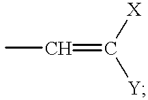
and R1 to R12 have the same meanings as above.
In those, R1 and R2, R3 and R4, R3′ and R4′, R5 and R6, R7 and R8, R9 and R10, R9′ and R10′, and R11 and R12 each may be or may not be bonded to each other to form a saturated or unsaturated, 5-membered or 6-membered ring. Optionally, they may be bonded to each other via a hetero atom (N, O, S) to form the ring.
R2 and R3, R4 and R3′, R4′ and R5, R8 and R9, R10 and R9′, and R10′ and R11 each may be or may not be bonded to each other to form a saturated or unsaturated, 5-membered or 6-membered ring. Optionally, they may be bonded to each other via a hetero atom (N, O, S) to form the ring.
As specific examples where R2 and R3, R10 and R9′, and R4′ and R5 each are bonded to each other to form a saturated 5-membered ring, mentioned are compounds of the following formula: 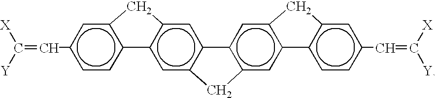
As those where R4 and R3′, and R10 and R9′ each are bonded to each other to form a saturated 6-membered ring, mentioned are compounds of the following formula: 
As those where R10 is a group of: 
and R9′ is a hydrogen atom to give a 5-membered ring, mentioned are compounds of the following formula: 
Where k=m=n=1 in formula (I), the compounds are represented by the following formula: 
wherein R3″, R4″, R9″ and R10″ each independently represents a hydrogen atom, an alkyl group having from 1 to 6 carbon atoms, an alkoxy group having from 1 to 6 carbon atoms, an aryloxy group having f rom 6 to 18 carbon atoms, an aryl group having f rom 6 to 20 carbon atoms, an amino group, an alkylamino group, an arylamino group, a cyano group, a nitro group, a hydroxyl group, a halogen atom, or a group of: 
and R1 to R12, R3′, R4′, R9′ and R10′ have the same meanings as above.
In those, R1 and R2, R3 and R4, R3′ and R4′, R3″ and R4″, R5 and R6, R7 and R8, R9 and R10, R9′ and R10′, R9″ and R10″, and R11 and R12 each may be or may not be bonded to each other to form a saturated or unsaturated, 5-membered or 6-membered ring. Optionally, they may be bonded to each other via a hetero atom (N, O, S) to form the ring.
R2 and R3, R4 and R3′, R4′ and R3″, R4″ and R5, R8 and R9, R10 and R9′, R10′ and R9″, and R10″ and R11 each may be or may not be bonded to each other to form a saturated or unsaturated, 5-membered or 6-membered ring. Optionally, they may be bonded to each other via a hetero atom (N, O, S) to form the ring.
As specific examples where R8, R9, R10″ and R11 each are a group of: 
to form an unsaturated 5-membered ring, and R3′ and R4′ together form a saturated 5-membered ring via a hetero atom N, mentioned are compounds of the following formula: 
X and Y each independently represent an aryl group having from 6 to 20 carbon atoms, such as a substituted or unsubstituted phenyl, naphthyl, biphenyl, terphenyl, anthraryl, phenathryl, pyrenyl or perylenyl group.
The substituent includes, for example, an alkyl group having from 1 to 6 carbon atoms, such as a methyl group, an ethyl group, an n-propyl group, an i-propyl group, an n-butyl group, an i-butyl group, a sec-butyl group, a t-butyl group, an i-pentyl group, a t-pentyl group, a neopentyl group, an n-hexyl group, an i-hexyl group; an alkoxy group having from 1 to 6 carbon atoms, such as a methoxy group, an ethoxy group, an n-propoxy group, an i-propoxy group, an n-butyloxy group, an i-butyloxy group, a sec-butyloxy group, an i-pentyloxy group, a t-pentyloxy group, an n-hexyloxy group; an aryloxy group having from 6 to 18 carbon atoms, such as a phenoxy group, a naphthyloxy group; a phenyl group, an amino group, an alkylamino group, an arylamino group, a cyano group, a nitro group, a hydroxyl group; and a halogen atom, such as a fluorine atom, a chlorine atom, a bromine atom, an iodine atom. The group of X and Y may be substituted with one or more of those substituents.
X and Y and optionally their substituents may be bonded together to form a substituted or unsubstituted, saturated 5-membered, or saturated 6-membered ring. As specific examples of the styryl compounds where X and Y form a saturated, 5-membered or 6-membered ring, mentioned are the following compounds where X and Y form a saturated 5-membered ring, k=m=1 and n=0: 
As those where X and Y form a saturated 6-membered ring, mentioned are the following compounds: 
In the invention, the organic blue-emitting layer must indispensably have a glass transition temperature of not lower than 75° C. Therefore, the organic host compounds to be in the layer are preferably selected from those of the following general formula (II) in which the central polyphenylene skeletons are all bonded to the adjacent ones at their para-positions: 
wherein R1 to R12, R3′, R4′, R9′, R10′, R3″, R4″, R9″, R10″, X, Y, k, m and n have the same meanings as above.
The styryl compounds of formula (I) can be produced by various known methods. For producing these, for example, mentioned are the following three methods.
Method 1
A phosphonate of a general formula (a): 
wherein k, m and n each are 0 or 1, and (k+m+n)≧1;
R1 to R12, R3′, R4′, R9′, R10′, R31″, R4″, R9″ and R10″ have the same meanings as above; and R represents an alkyl group having from 1 to 4 carbon atoms, or a phenyl group,
is condensed with a carbonyl group of a general formula (b): 
wherein X and Y have the same meanings as above, in the presence of a base through Wittig reaction or Wittig-Horner reaction to give styryl compounds of formula (I).
Method 2
A dialdehyde compound of a general formula (c): 
wherein k, m and n each are 0 or 1, and (k+m+n)≧1;
and R1 to R12, R3′, R4′, R9′, R10′, R31″, R4″, R9″ and R10″ have the same meanings as above,
is condensed with a phosphonate of a general formula (d): 
wherein R, X and Y have the same meanings as above, in the presence of a base through Wittig reaction or Wittig-Horner reaction to give styryl compounds of formula (I).
As the reaction solvent for that condensation, preferred are hydrocarbons, alcohols, and ethers. Specific examples of the solvent are methanol, ethanol, isopropanol, butanol, 2-methoxyethanol, 1,2-dimethoxyethane, bis(2-methoxyethyl)ether, dioxane, tetrahydrofuran(THF), toluene, and xylene. Also preferably employed are dimethylsulfoxide, N,N-dimethylformamide, N-methylpyrrolidone, 1,3-dimethyl-2-imidazolidinone, etc. Especially preferred are tetrahydrofuran and dimethylsulfoxide.
As the condensing agent, preferred are sodium hydroxide, potassium hydroxide, sodium amide, sodium hydride, n-butyl lithium, and even alcoholates such as sodium methylate, potassium t-butoxide, etc. Especially preferred are n-butyl lithium and potassium t-butoxide.
The reaction temperature varies, depending on the starting compounds to be reacted, and therefore cannot be defined indiscriminately. In general, however, it may be widely from 0° C. to about 100° C. Especially preferably, the reaction temperature falls between 0° C. and room temperature.
Method 3
A bromide of a general formula (e): 
wherein X, Y, R1, R2, R7, R8, and also R5, R6, R11 and R12 have the same meanings as above,
is reacted with Mg to give a Grignard reagent, which is coupled with a dibromoarylene compound of a general formula (f): 
wherein k, m and n each are 0 or 1, and (k+m+n)≧1;
and R3, R4, R9, R10, R3′, R4′, R9′, R10′, R3″, R4″, R9″ and R10″ have the same meanings as above,
in the presence of a metal catalyst to give styryl compounds of formula (I).
As the metal catalyst for the coupling, employable is a transition metal complex catalyst. Preferred are nickel catalysts and palladium catalysts, which include, for example, NiCl2 (dppp) (Tokyo Kasei), [NiCl2(PPh3)2], and also PdCl2 (dppf), and Pd(PPh3)4.
As the reaction solvent, employable is any of dewatered diethyl ether, THF, di-n-propyl ether, di-n-butyl ether, di-i-propyl ether, diethylene glycol dimethyl ether (diglyme), dioxane, dimethoxyethane (DME), etc.
Preferred are diethyl ether and THF.
Specific examples (1) to (61) of the styryl compounds for use in the invention are mentioned below, which, however, are not intended to restrict the scope of the invention. 


In the invention, one or more of those organic host compounds may be used either singly or as combined.
The fluorescent substance which is the other component constituting the organic blue-emitting layer is doped into the organic light-emitting layer in order to improve the efficiency of the organic EL device and to prolong the life thereof. The fluorescent substance is not specifically defined, provided that it can emit light in response to the recombination of holes and electrons, and may be any known fluorescent dye. However, it is important that the fluorescent substance is so selected that its energy gap is smaller than the energy gap of the organic host compound. The fluorescent substance includes, for example, stilbene derivatives, tristyrylarylene derivatives, and distyrylarylene derivatives (see Japanese Patent Application Laid-Open No. 5-129438). In the invention, one or more such fluorescent substances can be used either singly or as combined.
The organic host compound and the fluorescent substance are suitably selected and combined to give the organic blue-emitting layer, in which the efficient energy transfer from the organic host compound to the fluorescent substance is realized to attain the improvement in the efficiency of the organic EL device and the prolongation of the life thereof. In that preferred case, it has been found that the profile of the EL spectrum quite agrees with that of the fluorescence spectrum of the fluorescent substance within a range of ±10 nm with respect to the fluorescence peak wavelengths and the individual peak wavelengths of the vibronic structure. The fluorescence spectrum of the fluorescent substance is measured in a solution of the fluorescent substance as dissolved in a non-polar solvent such as toluene. When the profile of the EL spectrum quite agrees with that of the fluorescence spectrum of the fluorescent substance, it is herein referred that the EL device has “monomeric light-emitting ability”.
In the organic EL device of the invention having the monomeric light-emitting ability, it is meant that the initial state of EL corresponds to the excited monomeric state of the fluorescent substance in the organic light-emitting layer.
In order to improve the luminous efficiency of the organic EL device, it is effective to increase the fluorescence quantum efficiency of the organic host compound in the device. In the invention, therefore, that quantum efficiency must be not smaller than 0.3. The fluorescence quantum efficiency of the organic host compound is measured in a thin film of the substance, and is different from that as measured in its solution.
The organic EL device of the invention must retain a monomeric blue-emitting ability. Therefore, the organic host compound and the fluorescent substance are selected such that the interaction between the organic host compound and the fluorescent substance is absent and the interaction between the organic host compound and the adjacent compound layers is absent. As for blue-emitting organic host compounds, the interaction between the organic host compound and the fluorescent substance existing in the emitting layer and the interaction between the organic host compound and the adjacent organic compound layers are often large in many cases, in those cases the state having energy smaller than the energy of an excited state of the fluorescent substance is formed (an exciplex) . As a result, in those cases, the energy of the excited state of the fluorescent substance is transferred to the state having smaller energy, whereby the EL device gives a broad emission spectrum which, being different from the fluorescence spectrum of the monomeric emission from the fluorescent substance, has peaks at longer wavelengths. Even if the EL devices of those cases could produce monomeric emission in the initial stage of their driving, the light as emitted by them will often become different from monomeric one while the devices are continuously driven for long. Such EL devices that could not retain the ability of monomeric emission shall have an extremely short life.
Therefore, in the organic EL device of the invention, it is extremely important to select the combination of the organic host compound and the fluorescent substance so that the device can retain the ability of monomeric emission.
In addition, all the organic compound layers constituting the organic EL device of the invention must have a glass transition temperature of not lower than 75° C., in order to make the device have good heat resistance. Moreover, in order to further improve the storage stability of the device at 75° C., the stability of the interfaces between the organic light-emitting layer and the adjacent organic compound layers is an important factor. Therefore, the organic compound layers adjacent to the organic light-emitting layer must have a glass transition temperature of not lower than 105° C. If satisfying those requirements, the organic EL device is free from the change in the color to be emitted by it and from the reduction in the efficiency of the device, while maintaining its good properties for long, even though stored in a high-temperature atmosphere at 75° C.
The layer constitution of the organic EL device of the invention is not specifically defined, and may be any desired one. Basically, however, the organic blue-emitting layer is sandwiched between a pair of electrodes (positive electrode and negative electrode), in which are optionally provided a hole injection and transportation layer and an electron injection layer. Those are formed on a transparent substrate, through which the light emitted is seen. Examples of the organic EL device having that layer constitution are mentioned below.
(1) Positive electrode/organic light-emitting layer/negative electrode
(2) Positive electrode/hole injection layer/organic light-emitting layer/negative electrode
(3) Positive electrode/organic light-emitting layer/electron injection layer/negative electrode
(4) Positive electrode/hole injection layer/organic light-emitting layer/electron injection layer/negative electrode
(5) Positive electrode/hole injection layer/hole transportation layer/organic light-emitting layer/electron injection layer/negative electrode
In these structures, the organic compound layers such as the hole injection layer, the hole transportation layers and the electron injection layer are not specifically defined, provided that they satisfy the requirements for their glass transition temperature.
The organic EL device of the invention is optionally provided with a hole injection and transportation layer, which functions to inject holes thereinto from the positive electrode and to transport them into the light-emitting layer. Preferably, the hole injection and transportation layer has a hole mobility of not smaller than 10−6 cm2/V·s in an electric field of from 104 to 106 V/cm. If desired, the organic EL device may be provided with a laminate of a hole injection layer and a hole transportation layer.
The material to be in the hole injection and transportation layer may be selected from, for example, compounds of a general formula (III): 
In formula (III), Q1 and Q2 each represent a group having a nitrogen atom and at least three carbon rings (of which at least one is an aromatic ring such as a phenyl group), and these maybe the same or different; G represents a cycloalkylene group, an arylene group, or a linking group comprising a carbon-carbon bond.
In the organic EL device of the invention, the hole injection layer and the hole transportation layer that are directly adjacent to the organic light-emitting layer must have a glass transition temperature of not lower than 105° C. Therefore, the materials of those layers are preferably selected from oligomer amines of the compounds of formula (III) comprising three or more arylamines as bonded in a linear or branched manner.
The compounds of that type are, for example, represented by the following general formula (IV): 
wherein R13 to R17 each represent an alkyl group, an alkoxy group or a phenyl group, and may be the same or different, the phenyl substituent being optionally condensed with the group on which it is substituted to give a naphthyl group.
Specific examples of the compounds are mentioned below. 

The layers may comprise one or more of those compounds either singly or as combined.
The organic EL device of the present invention is optionally provided with an electron injection layer (electron injection and transportation layer), which functions to transfer the electrons as injected thereinto from the negative electrode to the organic light-emitting layer, and may comprise any known conventional electron-transmitting compound. For example, the material to be in the layer is preferably selected from metal complexes of 8-hydroxyquinoline or its derivatives, or oxadiazole derivatives.
As examples of metal complexes of 8-hydroxyquinoline or its derivatives, mentioned are metal chelate oxanoid compounds containing chelates of oxine (generally, 8-quinolinol or 8-hydroxyquinoline), etc. Compounds of that type all have a glass transition temperature of not lower than 105° C.
The electron injection layer may comprise one or more of those compounds either singly or as combined.
Preferably, the organic EL device of the invention having the constitution mentioned above is supported by a substrate, and the substrate in this use is not specifically defined. Any ordinary substrate for conventional organic EL devices is employable herein. For example, employed is any of glass or transparent plastics.
The positive electrode constituting the organic EL device of the invention is to inject holes into the device. For this, preferred are electrode materials having a large work function (not smaller than 4 eV), such as metals, alloys, electroconductive compounds and their mixtures. Specific examples of such preferred electrode materials are metals such as Au, and electroconductive transparent materials such as CuI, ITO (indium tin oxide), SnO2, ZnO, etc. The positive electrode can be formed, for example, through vacuum vapor deposition or sputtering of such an electrode material to give a thin film. For light emission through the electrode, it is preferred that the electrode has a transmittance, relative to the light emitted, of not smaller than 10%, and that the sheet resistance of the electrode is not larger than hundreds of ohms per square (Ω/□).
The thickness of the electrode film may be generally between 10 nm and 1 μm, preferably between 50 and 200 nm, depending on the material of the electrode.
The negative electrode constituting the organic EL device of the invention is to inject electrons into the device. For this, preferred are electrode materials having a small work function (not larger than 4 eV), such as metals, alloys, electroconductive compounds and their mixtures. Specific examples of such preferred electrode materials are sodium, sodium/potassium alloys, magnesium, lithium, magnesium/copper mixtures, magnesium/silver alloys, aluminium/lithium alloys, Al/Al2O3 mixtures, indium, rare earth metals, etc. The negative electrode can be formed, for example, through vacuum vapor deposition or sputtering of such an electrode material to give a thin film. For light emission through the electrode, it is preferred that the electrode has a transmittance, relative to the light emitted, of not smaller than 10%, and that the sheet resistance of the electrode is not larger than hundreds of ohms per square (Ω/□). The thickness of the electrode film may be generally between 10 nm and 1 μm, preferably between 50 and 200 nm, depending on the material of the electrode.
Now, preferred embodiments of producing the organic EL device of the invention are referred to hereinunder. First, a thin film of a desired electrode material, for example, a positive electrode material is formed on a suitable substrate through vapor deposition or sputtering to have a thickness of from 50 to 200 nm. This is formed a positive electrode on the substrate. Next, thin films of a hole injection layer, a hole transportation layer, an organic blue-emitting layer, and an electron injection layer are formed on the positive electrode.
To form those thin films, for example, employable is any of spin-coating, casting or vapor deposition. Preferred is vacuum vapor deposition, through which uniform films with few pin holes are easy to obtain. For the vapor deposition to form those thin films, the condition varies, depending on the type of the compound to be vaporized for the deposition, and the intended crystal structure and association structure of the molecular film to be deposited, but is preferably such that the boat heating temperature falls between 50 and 400° C., the vacuum degree falls between 10−6 and 10−3 Pa, the deposition rate falls between 0.01 and 50 nm/sec, the substrate temperature falls between −50 and 300° C., and the film thickness falls between 5 nm and 5 μm.
After the formation of those layers, a thin film of a negative electrode material is formed thereover, for example, through vapor deposition or sputtering to be a negative electrode having a film thickness of from 10 nm to 1 μm, preferably from 50 to 200 nm. Thus is produced the intended organic EL device. To produce the device, the order of forming the electrodes and the layers may be reversed.
Where a direct current voltage is applied to the organic EL device thus produced in that manner, a voltage of from 3 to 40 V or so may be applied thereto with its positive electrode being charged to be plus (+) and its negative electrode to be minus (−), whereby the device emits blue. Even if the same voltage is applied to the device in the reversed manner relative to the polarity of the electrodes, the device emits no light. Where an alternating current is applied to the device, the device emits light only when its positive electrode is charged to be plus (+) and its negative electrode to be minus (−). The wave mode of the alternating current to be applied to the device may be any desired one.
Now, the invention is described in more detail with reference to the following Examples, which, however, are not intended to restrict the scope of the invention.
(1) Production of Organic EL Device
A member comprising a 25 mm×75 mm×1.1 mm glass substrate and a 120 nm thick film electrode of ITO provided on the glass substrate was used as a transparent substrate. This was ultrasonically washed with isopropyl alcohol for 5 minutes, then washed with pure water for 5 minutes, and finally again ultrasonically washed with isopropyl alcohol for 5 minutes. Next, isopropyl alcohol was removed from the surface of the substrate by applying a dry nitrogen stream thereonto, and the substrate was then cleaned with ultraviolet rays with ozone.
This transparent substrate was mounted onto a substrate holder of a commercially-available vacuum vapor deposition system (manufactured by Nippon Vacuum Technology Co.). Five electrically-heating molybdenum boats were prepared, each of which was loaded with any of 500 mg of 4,4′-bis[N,N-di(m-tolyl)amino]-4″-phenyl-triphenylamine (TPD74), 500 mg of 4,4′-bis[N-phenyl-N-(1-naphthyl)-4-aminophenyl]triphenylamine (TPD78), 500 mg of 9,10-di[4-(2,2′-diphenylvinyl-1-yl)phenyl]anthracene (DPVDPAN), 500 mg of 4,4′-bis[2-(4-(N,N-diphenylamino)phenyl)vinyl]biphenyl (DPAVBi), and 100 mg of tris(8-hydroxyquinoline)aluminium (Alq).
The vacuum chamber of the system was degassed to have a reduced pressure of 1×10⁻⁴ Pa, in which the boat loaded with TPD74 was heated whereby TPD74 was deposited on the substrate to form thereon a hole injection layer having a thickness of 60 nm. Next, the boat loaded with TPD78 was heated to vaporize TPD78, whereby was formed a hole transportation layer having a thickness of 20 nm. Next, the boat laded with DPVDPAN and the boat loaded with DPAVBi were heated simultaneously to vaporize DPVDPAN and DPAVBi, whereby a light-emitting laminate layer having a thickness of 40 nm was formed on the hole transportation layer. The ratio by weight of DPVDPAN to DPAVBi in the light-emitting layer was 40/1. Finally, the boat loaded with Alq was heated to deposit Alq on the light-emitting layer, whereby was formed thereon an electron injection layer having a thickness of 20 nm.
Next, the sample thus produced was taken out of the vacuum chamber, and a mask of stainless steel was provided on the electron injection layer. This was again mounted onto the substrate holder, and a lithium/aluminium alloy matrix having a lithium concentration of 5 atm. %, from which is formed a negative electrode, was vaporized at a vacuum degree of 1×10⁻⁴ Pa and at a deposition rate of from 0.5 to 1.0 nm/sec to thereby form a negative electrode having a thickness of 150 nm.
(2) Light Emission Test of Organic EL Device
A direct current of 6 V was applied to the device thus obtained, with its ITO electrode being charged to be positive and its Al—Li alloy electrode to be negative, whereupon the device emitted uniform blue light.
Regarding the initial characteristics of the device at a voltage of 6 V and a current density of 1.9 mA/cm2, its luminance was 101 cd/m2, and its electric power conversion efficiency (luminous efficiency) was high to be 2.8 lm/W. Observing the device with the naked eye and with a luminometer (CS-100, manufactured by Minolta Co.), any non-emitting points were found on the light-emitting surface of the device and the device emitted light uniformly.
The EL spectrum of the device exhibited a vibrational structure, for which the individual peak wavelengths were the same as those in the fluorescence spectrum of the dopant (DPAVBi) from its toluene solution within a range of ±10 nm. The fluorescence quantum efficiency of the organic host compound, DPVDPAN in its thin film was 0.4.
This device was driven in a constant current condition in a nitrogen stream at an initial luminance of 100 cd/cm2, whereupon the half value period for it to have a luminance of 50 cd/cm2 was 3000 hours. During the driving test, there was no change in the color of the light emitted by the device, and it was found that the device retained the ability of monomeric light emission.
(3) Heat Resistance Test of Organic EL Device
The device was cased in a glass housing, into which was put an inert liquid(perfluoroether), and sealed. The thus-sealed device was stored in a thermo-hygrostat testing system at 75°0 C. At regular intervals, this was taken out, and its luminance, chromaticity and luminous efficiency were measured. The data thus measured verified that the light emitted by the device did not change at all for 500 hours or longer, and the device was stable for such a long time. In addition, the luminous efficiency of the device did not also change. From those, it is understood that the storage life of the device at 75° C. is 500 hours or longer, and that the thermal stability of the device is very good.
The materials used for the organic compound layers had a glass transition temperature, Tg, of 80° C. (TPD74), 126° C. (TPD78), 105° C. (DPVDPAN), 180° C. (Alq). Thus, Tg of all those organic compound layers was higher than 75° C., and Tg of the organic compound layers (TPD78, Alq), between which the light-emitting layer was sandwiched, was not lower than 105° C.
The data obtained herein are shown in Table 1, along with those obtained in the following Comparative Examples.
(1) Production of Organic EL Device
An organic EL device was produced in the same manner as in Example 1, except that N,N′-diphenyl-N,N′-bis(1-naphthyl)-[1,1′biphenyl]-4,4′-diamine (NPD) was used to form the hole transportation layer.
(2) Light Emission Test of Organic EL Device
Regarding the initial characteristics of the device at a voltage of 6 V and a current density of 1.9 mA/cm2, its luminance was 100 cd/m2, and its electric power conversion efficiency (luminous efficiency) was high to be 2.8 lm/W. Observing the device with the naked eye and with a luminometer (CS-100, manufactured by Minolta Co.), any non-emitting points were found on the light-emitting surface of the device and the device emitted light uniformly.
The EL spectrum of the device exhibited a vibrational structure, for which the individual peak wavelengths were the same as those in the fluorescence spectrum of the dopant (DPAVBi) from its toluene solution within a range of ±10 nm.
This device was driven in a constant current condition in a nitrogen stream at an initial luminance of 100 cd/cm2, whereupon the half value period for it to have a luminance of 50 cd/cm2 was 3000 hours. During the driving test, there was no change in the color of the light emitted by the device, and it was found that the device retained the ability of monomeric light emission.
These data indicate that the luminous efficiency and the life of this device are almost the same as those of the device of Example 1.
(3) Heat Resistance Test of Organic EL Device
This device was sealed and stored at 75° C. in the same manner as in Example 1. After having been thus stored for 150 hours, the color of the light emitted by the device changed, and the luminous efficiency of the device decreased to the half of the original one.
The glass transition temperature of NPD used herein was 100° C. The data obtained in this heat resistance test indicate that, even though all the organic compound layers constituting the device have a glass transition temperature of not lower than 75° C., only such is unsatisfactory for the heat resistance of the device in storage at 75° C. The difference between this device and the device of Example 1 is only in the hole transportation layer. Considering this, it is understood that, for the thermal stability of the organic EL device, the thermal stability of the organic compound layers adjacent to the light-emitting layer, or that is, their glass transition temperature is especially critical.
(1) Production of Organic EL Device
An organic EL device was produced in the same manner as in Example 1, except that 4,4′-bis (2,2′-diphenylvinyl)biphenyl (DPVBi) was used as the organic host compound in place of DPVDPAN.
(2) Light Emission Test of Organic EL Device
Regarding the initial characteristics of the device at a voltage of 6 V and a current density of 1.4 mA/cm2, its luminance was 102 cd/m2, and its electric power conversion efficiency (luminous efficiency) was high to be 3.8 lm/W. Observing the device with the naked eye and with a luminometer (CS-100, manufactured by Minolta Co.), any non-emitting points were found on the light-emitting surface of the device and the device emitted light uniformly.
This device gave monomeric EL. The fluorescence quantum efficiency of the thin film of DPVBi was 0.4.
This device was driven in a constant current condition in a nitrogen stream at an initial luminance of 100 cd/cm2, whereupon the half value period for it to have a luminance of 50 cd/cm2 was 2500 hours. During the driving test, there was no change in the color of the light emitted by the device, and it was found that the device retained the ability of monomeric light emission.
These data indicate that the luminous efficiency and the life of this device are almost the same as those of the device of Example 1.
(3) Heat Resistance Test of Organic EL Device
After having been stored at 75° C. in the same manner as in Example 1, the color of the light emitted by the device changed in 20 hours, and the luminous efficiency of the device reduced greatly. The reason is because the material of the light-emitting layer, DPVBi has a low glass transition temperature of 64° C.
(1) Production of Organic EL Device
An organic EL device was produced in the same manner as in Example 1, except that DBuPVBi was used as the organic host compound in place of DPVDPAN.
DBuPVBi was prepared by introducing tert-butyl group into the para-position of the both terminal phenyl groups of DPVBi, which was used in Comparative Example 2, in order to elevate its glass transition temperature. DBuPVBi thus had a glass transition temperature of 100° C.
(2) Light Emission Test of Organic EL Device
Regarding the initial characteristics of the device at a voltage of 6 V and a current density of 1.5 mA/cm2, its luminance was 103 cd/m2, and its electric power conversion efficiency (luminous efficiency) was high to be 3.6 lm/W. Observing the device with the naked eye and with a luminometer (CS-100, manufactured by Minolta Co.), any non-emitting points were found on the light-emitting surface of the device and the device emitted light uniformly.
This device gave monomeric EL. The fluorescence quantum efficiency of the thin film of DBuPVBi was 0.4.
The device was driven in a constant current condition in a nitrogen stream at an initial luminance of 100 cd/cm2, whereupon its luminance decreased to the half of the original one and the color emitted by the device changed. The emission spectrum of the thus-changed device differed from the initial EL spectrum of the original device, in that the former was broad while having peaks in the longer wavelength range.
These data indicate that, even though the introduction of a bulky substituent into an organic compound is effective in elevating the glass transition temperature of the resulting compound, the life of the device comprising the compound having such a bulky substituent shall be extremely short when the device could not retain the ability of monomeric light emission. From those, it is understood that the selection of the light-emitting material to make the device have the ability of monomeric light emission is extremely critical.
(1) Production of Organic EL Device
An organic EL device was produced in the same manner as in Example 1, except that bis(2-methyl-8-quinolato)(p-phenylphenolato)aluminium (PC7) was used as the organic host compound in place of DPVDPAN and that perylene was used as the fluorescent substance in place of DPAVBi.
(2) Light Emission Test of Organic EL Device
Regarding the initial characteristics of the device at a voltage of 6 V and a current density of 9.8 mA/cm2, its luminance was 100 cd/m2, and its electric power conversion efficiency (luminous efficiency) was 0.53 lm/W, or that is, it was lower than 1 lm/W. Observing the device with the naked eye and with a luminometer (CS-100, manufactured by Minolta Co.), any non-emitting points were found on the light-emitting surface of the device and the device emitted light uniformly.
The EL spectrum of the device exhibited a vibrational structure, for which the individual peak wavelengths were the same as those in the fluorescence spectrum of the dopant (perylene) from its toluene solution within a range of ±10 nm.
This device was driven in a constant current condition in a nitrogen stream at an initial luminance of 100 cd/cm2, whereupon the half value period for it to have a luminance of 50 cd/cm2 was 1500 hours. During the driving test, there was no change in the color of the light emitted by the device, and it was found that the device retained the ability of monomeric light emission.
However, as in the above, the luminous efficiency of this device is extremely low. The fluorescence quantum efficiency of the thin film of PC7 was 0.07. From those data obtained herein, it is understood that the high fluorescence quantum efficiency of the organic host compound used is indispensable for increasing the efficiency of the organic EL device.
| TABLE 1 | ||||||
| Ability of | ||||||
| Efficiency | Monomeric Light | Tg (° C.) | Stored at 75° C. | |||
| (lumen/W) | Emsission1) | HTL2) | Host | Life (hrs) | (hrs) | ||
| Example 1 | 2.8 | ◯ | 126 | 105 | 3000 | 500 or longer |
| Comparative | 2.8 | ◯ | 100 | 105 | 3000 | 150 |
| Example 1 | ||||||
| Comparative | 3.8 | ◯ | 126 | 64 | 2500 | 20 |
| Example 2 | ||||||
| Comparative | 3.6 | X | 126 | 100 | several minutes | not measured |
| Example 3 | ||||||
| Comparative | 0.53 | ◯ | 126 | 100 | 1500 | 500 |
| Example 4 | ||||||
| Notes: | ||||||
| 1)Ability of Monomeric Light Emission | ||||||
| ◯: The sample retained the ability of monomer light emission. | ||||||
| X: The sample did not retain the ability of monomeric light emission. | ||||||
| 2)HTL: hole transportation layer | ||||||
As has been mentioned hereinabove, the organic, blue-emitting EL device of the invention has a long life and has high luminous efficiency and good thermal stability. The device is favorably used in various displays.
While the invention has been described in detail and with reference to specific embodiments thereof, it will be apparent to one skilled in the art that various changes and modifications can be made therein without departing from the spirit and scope thereof.
Claims (7)
1. An organic host compound represented by the following formula (I): 
wherein, R1 to R12 each independently represent a hydrogen atom, an alkyl group having from 1 to 6 carbon atoms, an alkoxy group having from 1 to 6 carbon atoms, an aryloxy group having from 6 to 18 carbon atoms, an aryl group having from 6 to 20 carbon atoms, an amino group represented by —NH2, an alkylamino group represented by —NHR or —NR2 (where R indicates an alkyl group having from 1 to 6 carbon atoms), an arylamino group represented by —NHAr or —NAr2 (where Ar indicates an aryl group having from 6 to 20 carbon atoms), a cyano group, a nitro group, a hydroxyl group, a halogen atom, or a group of: 
the substituents in at least one combination of R1 and R2, R3 and R4, R5 and R6, R7 and R8, R9 and R10, and R11 and R12 are bonded to each other to form a saturated or unsaturated, 5-membered or 6-membered ring; and the substituents may be bonded via a hetero atom (N, O, S) to form the ring.
2. The organic host compound in claim 1 , in which R3 and R4, and R9 and R10 each are bonded to each other to form an unsaturated 5-membered ring or an unsaturated 6-membered ring.
3. An organic host compound selected from the group consisting of compounds represented by the following formulae (1)-(18) and (59): 


4. An organic host compound represented by the following formula (II): 
wherein R3′, R4′, R9′ and R10′ each independently represent a hydrogen atom, an alkyl group having from 1 to 6 carbon atoms, an alkoxy group having from 1 to 6 carbon atoms, an aryloxy group having from 6 to 18 carbon atoms, an aryl group having from 6 to 20 carbon atoms, an amino group, an alkylamino group, an arylamino group, a cyano group, a nitro group, a hydroxyl group, a halogen atom, or a group of: 
and R1 to R12 have the same meanings as above; R1 and R2, R3 and R4, R3′ and R4′, R5 and R6, R7 and R8, R9 and R10, R9′ and R10′, and R11 and R12 each may be or may not be bonded to each other to form a saturated or unsaturated, 5-membered or 6-membered ring, optionally they may be bonded to each other via a hetero atom (N, O, S) to form the ring; and R2 and R3, R4 and R3′, R4′ and R5, R8 and R9, R10 and R9′, and R10′ and R11 each may be or may not be bonded to each other to form a saturated or unsaturated, 5-membered or 6-membered ring, optionally, they may be bonded to each other via a hetero atom (N, O, S) to form the ring.
5. An organic host compound selected from the group consisting of compounds represented by the following formulae (19)-(48) and (60): 


6. An organic host compound represented by the following formula (III): 
wherein R3″, R4″, R9″ and R10″ each independently represents a hydrogen atom, an alkyl group having from 1 to 6 carbon atoms, an alkoxy group having from 1 to 6 carbon atoms, an aryloxy group having from 6 to 18 carbon atoms, an aryl group having from 6 to 20 carbon atoms, an amino group, an alkylamino group, an arylamino group, a cyano group, a nitro group, a hydroxyl group, a halogen atom, or a group of: 
and R1 to R12, R3′, R4′, R9′ and R10′ have the same meanings as above; R1 and R2, R3 and R4, R3′ and R4′, R3″ and R4″, R5 and R6, R7 and R8, R9′ and R10′, R9″ and R10″, and R11 and R12 each may be or may not be bonded to each other to form a saturated or unsaturated, 5-membered or 6-membered ring, optionally they may be bonded to each other via a hetero atom (N, O, S) to form the ring; and R2 and R3, R4 and R3′, R4′ and R3″, R4″ and R5, R8 and R9, R10 and R9′, R10′ and R9″, and R10″ and R 11 each may be or may not be bonded to each other to form a saturated or unsaturated, 5-membered or 6-membered ring, optionally, they may be bonded to each other via a hetero atom (N, O, S) to form the ring.
7. An organic host compound selected from the group consisting of compounds represented by the following formulae (49)-(58) and (61): 


Priority Applications (1)
| Application Number | Priority Date | Filing Date | Title |
|---|---|---|---|
| US09/778,816 US6489489B2 (en) | 1996-10-08 | 2001-02-08 | Organic electroluminescent device |
Applications Claiming Priority (4)
| Application Number | Priority Date | Filing Date | Title |
|---|---|---|---|
| JP26702196A JP3228502B2 (en) | 1996-10-08 | 1996-10-08 | Organic electroluminescence device |
| JP8-267021 | 1996-10-08 | ||
| US08/941,036 US6214481B1 (en) | 1996-10-08 | 1997-09-30 | Organic electroluminescent device |
| US09/778,816 US6489489B2 (en) | 1996-10-08 | 2001-02-08 | Organic electroluminescent device |
Related Parent Applications (1)
| Application Number | Title | Priority Date | Filing Date |
|---|---|---|---|
| US08/941,036 Division US6214481B1 (en) | 1996-10-08 | 1997-09-30 | Organic electroluminescent device |
Publications (2)
| Publication Number | Publication Date |
|---|---|
| US20010019783A1 US20010019783A1 (en) | 2001-09-06 |
| US6489489B2 true US6489489B2 (en) | 2002-12-03 |
Family
ID=17438961
Family Applications (2)
| Application Number | Title | Priority Date | Filing Date |
|---|---|---|---|
| US08/941,036 Expired - Lifetime US6214481B1 (en) | 1996-10-08 | 1997-09-30 | Organic electroluminescent device |
| US09/778,816 Expired - Lifetime US6489489B2 (en) | 1996-10-08 | 2001-02-08 | Organic electroluminescent device |
Family Applications Before (1)
| Application Number | Title | Priority Date | Filing Date |
|---|---|---|---|
| US08/941,036 Expired - Lifetime US6214481B1 (en) | 1996-10-08 | 1997-09-30 | Organic electroluminescent device |
Country Status (3)
| Country | Link |
|---|---|
| US (2) | US6214481B1 (en) |
| JP (1) | JP3228502B2 (en) |
| DE (1) | DE69714372T2 (en) |
Cited By (2)
| Publication number | Priority date | Publication date | Assignee | Title |
|---|---|---|---|---|
| US20070170843A1 (en) * | 2004-03-05 | 2007-07-26 | Idemitsu Kosan Co., Ltd. | Organic electroluminescent device and organic electroluminescent display |
| US20090167156A1 (en) * | 2007-02-28 | 2009-07-02 | Idemitsu Kosan Co., Ltd. | Organic electroluminescence device |
Families Citing this family (22)
| Publication number | Priority date | Publication date | Assignee | Title |
|---|---|---|---|---|
| JP3228502B2 (en) | 1996-10-08 | 2001-11-12 | 出光興産株式会社 | Organic electroluminescence device |
| TW521537B (en) | 1998-05-08 | 2003-02-21 | Idemitsu Kosan Co | Organic electroluminescence element |
| KR100280125B1 (en) * | 1998-11-17 | 2001-02-01 | 정선종 | New blue light-emitting polymer prepared by using a new tetraphenyl derivative substituted with fluorine as a monomer and an electroluminescent device using the same |
| US6656608B1 (en) * | 1998-12-25 | 2003-12-02 | Konica Corporation | Electroluminescent material, electroluminescent element and color conversion filter |
| TWI245064B (en) * | 1998-12-28 | 2005-12-11 | Idemitsu Kosan Co | Organic electroluminescence device |
| JP3983405B2 (en) * | 1999-01-19 | 2007-09-26 | 出光興産株式会社 | Organic electroluminescence device and method for manufacturing the same |
| KR100702763B1 (en) * | 1999-02-15 | 2007-04-03 | 이데미쓰 고산 가부시키가이샤 | Organic electroluminescent device and method of manufacture thereof |
| JP4573923B2 (en) * | 1999-04-27 | 2010-11-04 | 三井化学株式会社 | Amine compounds |
| JP2006287248A (en) * | 1999-09-21 | 2006-10-19 | Idemitsu Kosan Co Ltd | Organic electroluminescence element and organic luminous medium |
| EP1167488B1 (en) * | 1999-09-21 | 2007-04-25 | Idemitsu Kosan Company Limited | Organic electroluminescent device and organic luminous medium |
| KR100387166B1 (en) | 1999-12-15 | 2003-06-12 | 닛뽄덴끼 가부시끼가이샤 | Organic Electroluminescence Device |
| KR100478520B1 (en) * | 2001-08-13 | 2005-03-28 | 삼성에스디아이 주식회사 | Blue light-emitting compound and display device adopting light-emitting compound as color-developing substance |
| KR20050040835A (en) * | 2001-10-31 | 2005-05-03 | 이데미쓰 고산 가부시키가이샤 | Novel soluble compound and organic electroluminescent devices |
| US6818919B2 (en) | 2002-09-23 | 2004-11-16 | Air Products And Chemicals, Inc. | Light emitting layers for LED devices based on high Tg polymer matrix compositions |
| JP4152173B2 (en) * | 2002-11-18 | 2008-09-17 | 出光興産株式会社 | Organic electroluminescence device |
| US7862906B2 (en) | 2003-04-09 | 2011-01-04 | Semiconductor Energy Laboratory Co., Ltd. | Electroluminescent element and light-emitting device |
| TWI252055B (en) * | 2003-10-03 | 2006-03-21 | Pioneer Corp | Organic electroluminescent device |
| US20080207823A1 (en) * | 2004-12-29 | 2008-08-28 | E.I. Du Pont De Nemours And Company | Active Compositions And Methods |
| KR101412813B1 (en) * | 2007-05-29 | 2014-06-27 | 에스케이이노베이션 주식회사 | Organic electroluminescent polymer containing oxadiazole group and organic electroluminescent device manufactured using the same |
| JP5407241B2 (en) | 2007-09-28 | 2014-02-05 | 大日本印刷株式会社 | Electroluminescence element |
| WO2015117100A1 (en) | 2014-02-02 | 2015-08-06 | Molaire Consulting Llc | Noncrystallizable sensitized layers for oled and oeds |
| JP6693053B2 (en) | 2015-06-03 | 2020-05-13 | セイコーエプソン株式会社 | Light emitting element, light emitting device, authentication device, and electronic device |
Citations (7)
| Publication number | Priority date | Publication date | Assignee | Title |
|---|---|---|---|---|
| US4734338A (en) * | 1984-07-31 | 1988-03-29 | Canon Kabushiki Kaisha | Electroluminescent device |
| US5413887A (en) | 1991-10-17 | 1995-05-09 | Minolta Camera Kabushiki Kaisha | Distyryl compound and photosensitive member comprising the same |
| US5503910A (en) * | 1994-03-29 | 1996-04-02 | Idemitsu Kosan Co., Ltd. | Organic electroluminescence device |
| US5536949A (en) | 1992-08-28 | 1996-07-16 | Idemistu Kosan Co., Ltd. | Charge injection auxiliary material and organic electroluminescence device containing the same |
| US5601903A (en) * | 1993-08-27 | 1997-02-11 | Sanyo Electric Co., Ltd. | Organic electroluminescent elements |
| US6214481B1 (en) | 1996-10-08 | 2001-04-10 | Idemitsu Kosan Co., Ltd. | Organic electroluminescent device |
| US6224966B1 (en) | 1997-03-18 | 2001-05-01 | Idemitsu Kosan Co., Ltd. | Organic electroluminescent device |
Family Cites Families (2)
| Publication number | Priority date | Publication date | Assignee | Title |
|---|---|---|---|---|
| US5652067A (en) * | 1992-09-10 | 1997-07-29 | Toppan Printing Co., Ltd. | Organic electroluminescent device |
| US5554450A (en) * | 1995-03-08 | 1996-09-10 | Eastman Kodak Company | Organic electroluminescent devices with high thermal stability |
-
1996
- 1996-10-08 JP JP26702196A patent/JP3228502B2/en not_active Expired - Lifetime
-
1997
- 1997-09-30 US US08/941,036 patent/US6214481B1/en not_active Expired - Lifetime
- 1997-10-07 DE DE69714372T patent/DE69714372T2/en not_active Expired - Lifetime
-
2001
- 2001-02-08 US US09/778,816 patent/US6489489B2/en not_active Expired - Lifetime
Patent Citations (7)
| Publication number | Priority date | Publication date | Assignee | Title |
|---|---|---|---|---|
| US4734338A (en) * | 1984-07-31 | 1988-03-29 | Canon Kabushiki Kaisha | Electroluminescent device |
| US5413887A (en) | 1991-10-17 | 1995-05-09 | Minolta Camera Kabushiki Kaisha | Distyryl compound and photosensitive member comprising the same |
| US5536949A (en) | 1992-08-28 | 1996-07-16 | Idemistu Kosan Co., Ltd. | Charge injection auxiliary material and organic electroluminescence device containing the same |
| US5601903A (en) * | 1993-08-27 | 1997-02-11 | Sanyo Electric Co., Ltd. | Organic electroluminescent elements |
| US5503910A (en) * | 1994-03-29 | 1996-04-02 | Idemitsu Kosan Co., Ltd. | Organic electroluminescence device |
| US6214481B1 (en) | 1996-10-08 | 2001-04-10 | Idemitsu Kosan Co., Ltd. | Organic electroluminescent device |
| US6224966B1 (en) | 1997-03-18 | 2001-05-01 | Idemitsu Kosan Co., Ltd. | Organic electroluminescent device |
Non-Patent Citations (2)
| Title |
|---|
| Database WPI, Derwent Publications, AN 97-095426, JP 8-333283, Dec. 17, 1996. |
| Patent Abstract of Japan, vol. 17, No. 632 (C-1132), Nov. 24, 1993, JP 05-194943, Aug. 3, 1993. |
Cited By (2)
| Publication number | Priority date | Publication date | Assignee | Title |
|---|---|---|---|---|
| US20070170843A1 (en) * | 2004-03-05 | 2007-07-26 | Idemitsu Kosan Co., Ltd. | Organic electroluminescent device and organic electroluminescent display |
| US20090167156A1 (en) * | 2007-02-28 | 2009-07-02 | Idemitsu Kosan Co., Ltd. | Organic electroluminescence device |
Also Published As
| Publication number | Publication date |
|---|---|
| US20010019783A1 (en) | 2001-09-06 |
| JPH10110163A (en) | 1998-04-28 |
| DE69714372T2 (en) | 2003-01-30 |
| DE69714372D1 (en) | 2002-09-05 |
| US6214481B1 (en) | 2001-04-10 |
| JP3228502B2 (en) | 2001-11-12 |
Similar Documents
| Publication | Publication Date | Title |
|---|---|---|
| US6489489B2 (en) | Organic electroluminescent device | |
| US6224966B1 (en) | Organic electroluminescent device | |
| US6660411B2 (en) | Organic electroluminescent device | |
| JP4243876B2 (en) | Electroluminescent device | |
| US5942340A (en) | Indolocarbazole electroluminescent devices | |
| JP4407102B2 (en) | Anthracene compound, method for producing the same, and organic electroluminescent device | |
| JP3508984B2 (en) | Organic compound and light emitting device using the organic compound | |
| US7923129B2 (en) | Carbazole derivative and organic light emitting device using the same | |
| US20060014046A1 (en) | Luminescent material and organic electroluminescent device using the same | |
| US20060269780A1 (en) | Organic electroluminescent device | |
| JP2003031371A (en) | Organic electroluminescent element and blue light emitting element | |
| JP2002100482A (en) | Organic electroluminescence element | |
| JP2005011610A (en) | Organic electroluminescent element | |
| JP2000068057A (en) | Organic electroluminescent element | |
| JP2000021572A (en) | Organic electroluminescance element | |
| JP2004103467A (en) | Organic electroluminescent element | |
| JPWO2003050201A1 (en) | Organic electroluminescence element material | |
| JP4135411B2 (en) | Asymmetric 1,4-phenylenediamine derivative and organic electroluminescence device using the same | |
| EP0836366B1 (en) | Organic electroluminescent device | |
| JP4631122B2 (en) | Organic EL device | |
| JP2000003790A (en) | Organic electroluminescent element | |
| JP3757583B2 (en) | Organic electroluminescence device | |
| JPH11354284A (en) | Organic electroluminescence element | |
| JPH11302639A (en) | Organic electroluminescent element | |
| JPH11312587A (en) | Organic electroluminescent element |
Legal Events
| Date | Code | Title | Description |
|---|---|---|---|
| STCF | Information on status: patent grant |
Free format text: PATENTED CASE |
|
| FEPP | Fee payment procedure |
Free format text: PAYOR NUMBER ASSIGNED (ORIGINAL EVENT CODE: ASPN); ENTITY STATUS OF PATENT OWNER: LARGE ENTITY Free format text: PAYER NUMBER DE-ASSIGNED (ORIGINAL EVENT CODE: RMPN); ENTITY STATUS OF PATENT OWNER: LARGE ENTITY |
|
| FPAY | Fee payment |
Year of fee payment: 4 |
|
| FPAY | Fee payment |
Year of fee payment: 8 |
|
| FPAY | Fee payment |
Year of fee payment: 12 |