US6489860B1 - Surface acoustic wave duplexer with first and second package ground patterns - Google Patents
Surface acoustic wave duplexer with first and second package ground patterns Download PDFInfo
- Publication number
- US6489860B1 US6489860B1 US09/667,803 US66780300A US6489860B1 US 6489860 B1 US6489860 B1 US 6489860B1 US 66780300 A US66780300 A US 66780300A US 6489860 B1 US6489860 B1 US 6489860B1
- Authority
- US
- United States
- Prior art keywords
- package substrate
- acoustic wave
- surface acoustic
- ground potential
- duplexer
- Prior art date
- Legal status (The legal status is an assumption and is not a legal conclusion. Google has not performed a legal analysis and makes no representation as to the accuracy of the status listed.)
- Expired - Lifetime, expires
Links
Images


Classifications
-
- H—ELECTRICITY
- H03—ELECTRONIC CIRCUITRY
- H03H—IMPEDANCE NETWORKS, e.g. RESONANT CIRCUITS; RESONATORS
- H03H9/00—Networks comprising electromechanical or electro-acoustic devices; Electromechanical resonators
- H03H9/70—Multiple-port networks for connecting several sources or loads, working on different frequencies or frequency bands, to a common load or source
- H03H9/72—Networks using surface acoustic waves
- H03H9/725—Duplexers
-
- H—ELECTRICITY
- H03—ELECTRONIC CIRCUITRY
- H03H—IMPEDANCE NETWORKS, e.g. RESONANT CIRCUITS; RESONATORS
- H03H9/00—Networks comprising electromechanical or electro-acoustic devices; Electromechanical resonators
- H03H9/02—Details
- H03H9/05—Holders; Supports
- H03H9/0538—Constructional combinations of supports or holders with electromechanical or other electronic elements
- H03H9/0566—Constructional combinations of supports or holders with electromechanical or other electronic elements for duplexers
- H03H9/0576—Constructional combinations of supports or holders with electromechanical or other electronic elements for duplexers including surface acoustic wave [SAW] devices
-
- H—ELECTRICITY
- H03—ELECTRONIC CIRCUITRY
- H03H—IMPEDANCE NETWORKS, e.g. RESONANT CIRCUITS; RESONATORS
- H03H9/00—Networks comprising electromechanical or electro-acoustic devices; Electromechanical resonators
- H03H9/70—Multiple-port networks for connecting several sources or loads, working on different frequencies or frequency bands, to a common load or source
- H03H9/72—Networks using surface acoustic waves
Definitions
- the present invention relates to a Surface Acoustic Wave duplexer (hereinafter referred to as a SAW duplexer) employed in a high frequency Radio Frequency (RF) filter in a Surface Acoustic Wave resonance filter employed in small, portable communication equipment such as portable telephones.
- SAW duplexer Surface Acoustic Wave duplexer
- RF Radio Frequency
- a terminal connected to one end of the parallel arm SAW resonator of a SAW filter chip and a ground terminal of the SAW duplexer package are connected using bonding wiring while mounting the SAW filter chip on the SAW duplexer package.
- the object of the present invention is to bring about a small SAW duplexer while improving frequency characteristics of a SAW duplexer.
- a surface acoustic wave duplexer of the present invention comprises a first surface acoustic wave filter having a first pass frequency band region, a second surface acoustic wave filter having a second pass frequency band lower than the first pass frequency band and including a series arm surface acoustic wave resonator and a parallel arm surface acoustic wave resonator, a multi-layer package substrate including first to third package substrates, electrode pads formed on the first package substrate, a first ground potential pattern formed on the second package substrate, the first ground pattern being connected to the electrode pads and extending to a central region of the second package substrate and a second ground potential pattern formed on the third package substrate.
- One end of the parallel arm surface acoustic wave resonator is connected to ground potential via the electrode pads and the first and second ground potential patterns.
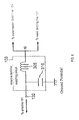
- FIG. 1 is a block diagram showing an outline of an example configuration of a SAW duplexer of a first embodiment of the present invention
- FIG. 2 is a view showing a configuration of a circuit for a SAW filter for transmission use having a low-band side pass frequency band of the first embodiment of the present invention
- FIG. 3 A and FIG. 3B are plan views of a SAW duplexer package substrate of the first embodiment of the present invention.
- FIG. 4 A and FIG. 4B are plan views of a SAW duplexer package substrate of the first embodiment of the present invention.
- FIG. 5 is a circuit diagram of a transmission input matching circuit of the first embodiment of the present invention.
- FIG. 6 is a circuit diagram of an antenna terminal matching circuit of the first embodiment of the present invention.
- FIG. 7 is a circuit diagram of a receiving output matching circuit of the first embodiment of the present invention.
- FIG. 8 is a view showing frequency characteristics of a SAW duplexer relating to the present invention.
- FIG. 9 is a view showing frequency characteristics of a SAW duplexer of the first embodiment of the present invention.
- FIG. 10 A and FIG. 10B are plan views of a SAW duplexer package substrate and a SAW duplexer sealing cap of a second embodiment of the present invention.
- FIG. 1 is a block diagram showing an outline of an example configuration of a SAW duplexer of a first embodiment of the present invention.
- a SAW duplexer 100 of the present invention comprises an antenna terminal matching circuit 103 , a transmission SAW filter 104 , a transmission input matching circuit 105 , a wave dividing line 107 , a receive SAW filter 108 , and a receiving output matching circuit 109 .
- the antenna terminal matching circuit 103 is connected across an antenna terminal 102 and a node N 1 .
- the transmission SAW filter 104 and the transmission input matching circuit 105 are connected across the node Ni and a transmission terminal 106 .
- the wave dividing line 107 , receive SAW filter 108 , and receiving output matching circuit 109 are connected across the node N 1 and a receiving terminal 110 .
- a power amplifier 111 is connected to the transmission terminal 106 and a receiving circuit 112 is connected to the receiving terminal 110 .
- a circuit configuration for a transmission SAW filter 104 being one of two SAW filters (the transmission SAW filter 104 and a receive SAW filter 108 ) having different pass frequency bands, is shown in FIG. 2 .
- the transmission SAW filter 104 has a second pass frequency band lower than the first pass frequency band of the receive SAW filter 108 .
- series arm SAW resonators 203 to 205 are connected in series across input terminals 201 A and 201 B, and output terminals 202 A and 202 B.
- a parallel arm SAW resonator 206 is connected across a node N 2 and node N 4 across the series arm SAW resonators 203 and 204
- a parallel arm SAW resonator 207 is connected across a node N 3 and node N 4 between the series arm SAW resonators 204 and 205 .
- An inductance circuit 208 and an inductance circuit 209 which is formed at the SAW duplexer package as a feature of the present invention are connected using bonding wire across the node N 4 and a node N 5 .
- inductance circuit 209 that is a main feature of the present invention is now described together with the SAW duplexer 100 and the SAW duplexer package structure, using FIG. 3A, FIG. 3B, FIG. 4 A and FIG. 4 B.
- FIG. 3A, FIG. 3B, FIG. 4 A and FIG. 4B are plan views of a SAW duplexer package substrate having a multi-layer structure for mounting the transmission SAW filter 104 and the receive SAW filter 108 .
- Each package substrate (first to fourth package substrates) on which the transmission input matching circuit 105 , wave dividing line 107 , and receiving output matching circuit 109 , etc., are formed within the SAW duplexer package substrate having the multi-layer structure of the present invention is described in FIGS. 3A and 3B and FIGS. 4A and 4B.
- a fourth package substrate 300 D shown in FIG. 4B is taken as the lowermost layer, with a third package substrate 300 C shown in FIG.
- a fifth package substrate 300 E and a sealing cap 300 F for sealing the SAW filter chip are formed as a layer on the first package substrate 300 A.
- a description of the structures of the fifth package substrate 300 E and the sealing cap 300 F is given in the second embodiment.
- a cavity (opening) 301 for building-in the SAW filter chip is provided at a central part of the first package substrate 300 A.
- Electrode pads 302 A to 302 K are formed at the periphery of the cavity 301 in order to connect the SAW filter chip and the SAW duplexer package.
- Electrode pads 302 A to 302 F are connected to the transmission SAW filter 104 and electrode pads 302 G to 302 K are connected to the receive SAW filter 108 .
- Through-holes 303 C to 303 L for obtaining a connection with the second package substrate 300 B are formed at the electrode pads 302 C to 302 J.
- a stripline 304 is formed so as to connect with the electrode pad 302 A, with a through-hole 303 A, described later, for obtaining a connection with a ground potential pattern 309 A formed on the second package substrate 300 B being formed midway.
- a stripline 305 corresponding to the antenna terminal matching circuit 103 is formed across an electrode pad 302 B and the antenna terminal 102 so as to function as a matching circuit having inductance.
- a through-hole 303 B for obtaining a connection with the wave dividing line 107 , provided at the third package substrate 300 C (described later) is provided midway along the stripline 305 .
- This through-hole 303 B corresponds to the node N 1 of the block diagram of the SAW duplexer shown in FIG. 1.
- a stripline 306 is provided as an inductance component between the electrode pad 303 E and the transmission terminal 106 .
- An open stub 307 having a capacitance component is connected to the transmission terminal 106 .
- a through-hole 303 E for obtaining a connection with the open stub 317 formed on the third package substrate 300 C (described later) is formed at the electrode pad 302 E.
- a stripline 308 constituting part of the receiving output matching circuit having an inductance component is provided between the electrode pad 302 K and the receiving terminal 110 .
- Interconnecting terminals, 314 A, 314 D and 314 G- 314 L, and grounded terminals, 314 B, 314 C, 314 E and 314 F, are formed at the periphery of the second package substrate 300 B.
- Ground potential patterns 309 A and 309 B are then formed on the second package substrate 300 B.
- the ground potential pattern 309 A is formed in such a manner as to not connect with interconnecting terminals, 314 A, 314 D and 314 G- 314 L, and grounded terminals, 314 B, 314 C, 314 E and 314 F and to extend into a region 315 for mounting the SAW filter chips.
- a plurality of through-holes 310 for obtaining connections with the fourth package substrate 300 D via the third package substrate 300 C are formed the extended region 315 .
- Connection points 311 A to 311 D existing in a region other than the extended region 315 of the ground potential pattern 309 A are provided for connecting with the through-holes 303 A, 303 C, 303 D and 303 F formed in the first package substrate 300 A.
- the ground potential pattern 309 B is connected to the grounded terminals 314 B and 314 C, and 314 E and 314 F.
- Connection points 311 E to 311 I on the ground potential pattern 309 B are for obtaining connections with the through-holes 303 G, 303 I to 303 K, and 303 L formed on the first package substrate 300 A.
- through-holes 312 and 313 for obtaining connections with the wave dividing line 107 on the third package substrate 300 C are formed at a region other than the region formed with the ground potential patterns 309 A and 309 B.
- Interconnecting terminals 322 B, 322 C and 322 E-L, and stub connected terminals, 322 A and 322 D, are formed about the periphery of the third package substrate 300 C.
- Connection points 320 and 321 on the third package substrate 300 C are for connecting with the stripline 305 and the electrode pad 302 H, respectively, on the first package substrate 300 A.
- the wave dividing line 107 is provided in such a manner as to provide a connection between the connection points 320 and 321 .
- the stub connected terminal 322 A is employed as the antenna terminal 102 and an open stub 316 having a capacitance component is connected to the stub connected terminal 322 A.
- the stub connected terminal 322 D is employed as the receiving terminal and an open stub 318 having a capacitance component is connected to the stub connected terminal 322 D.
- An open stub 317 is connected to connection point 326 of the third package substrate 300 C.
- the interconnecting terminals 322 B, 322 C, 322 E and 322 F are connected to the ground potential pattern 309 B via the grounded terminals 314 B, 314 C, 314 E and 314 F as a result of being painted at side surface portions with an electrically conductive substance.
- Interconnecting terminals, 325 A, 325 D and 325 J, and grounded terminals, 325 B, 325 C, 325 E-I, 325 K and 325 L, are formed about the periphery of the fourth package substrate 300 D.
- Pads 330 A to 330 L are provided at a region in the vicinity of the interconnecting terminals, 325 A, 325 D and 325 J, and grounded terminals, 325 B, 325 C, 325 E-I, 325 K and 325 L.
- a ground potential pattern 324 runs along substantially the whole surface of the fourth package substrate 300 D and connects to the grounded terminals 325 B and 325 C, 325 E to 3251 , and 325 K and 325 L.
- a plurality of through-holes 323 capable of connecting the ground potential pattern 309 A on the second package substrate 300 B and the ground potential pattern 324 of the fourth package substrate 300 D are provided at a central region of the fourth package substrate 300 D.
- the ground potential pattern 309 B of the second package substrate 300 B is connected to the ground potential pattern 324 via electrically conductive material applied to side surface portions of the grounded terminals 325 B and 325 C, 325 E and 325 F of the fourth package substrate 300 D, grounded terminals 314 B and 314 C, and 314 E and 314 F of the second package substrate 300 B, and interconnecting terminals 322 B and 322 C, 322 E and 322 F of the third package substrate 300 C.
- the interconnecting terminals 325 A, 325 D and 325 J are terminals used as the antenna terminal 102 , the receiving terminal 110 and the transmission terminal 106 , respectively.
- a SAW filter chip is mounted on the extended region 315 of a ground potential pattern of the second package substrate 300 B within a cavity 301 of the first package substrate 300 A.
- the inductance circuit 208 having an inductance due to the bonding wire is therefore formed across the node N 4 and the ground potential.
- the electrode pads 302 C and 302 F are therefore connected to ground potential via, in order, the through-holes 303 C and 303 F, the ground potential pattern 309 A of the second package substrate 300 B, the plurality of through-holes 310 , the ground potential pattern 324 formed on the fourth package substrate 300 D, and the grounded terminals 325 B and 325 C, 325 E to 3251 , 325 K and 325 L taken as ground terminals, i.e.
- the ground potential pattern 309 A on the second package substrate 300 B is connected to ground potential via the plurality of through-holes 310 formed at central regions of the second and third package substrates 300 B and 300 C and the ground potential pattern 324 , rather than via the interconnecting terminals, 314 A, 314 D, 314 G- 314 L, and grounded terminals, 314 B, 314 C, 314 E and 314 F at the periphery of the second package substrate 300 B.
- the distance from the wirebonded electrode pads 302 C and 302 F to ground potential can be made as large as possible and a new inductance circuit 209 , which is separate from the inductance circuit 208 and has an inductance component, can therefore be added across the node N 4 at transmission SAW filter 104 and ground potential.
- FIG. 8 is a view showing the frequency characteristics of a SAW filter for transmission of a related SAW duplexer
- FIG. 9 is a view showing the frequency characteristics of the transmission SAW filter 104 of the SAW duplexer of the first embodiment of the present invention.
- the horizontal axis denotes frequency (MHz)
- the vertical axis denotes attenuation (dB). Comparing the frequency characteristics of FIG. 8 and FIG.
- Attenuation is larger for the transmission SAW filter 104 of the first embodiment of the present invention.
- the attenuation for the related SAW filter for transmission is 42.295 dB but the attenuation for the transmission SAW filter 104 of the first embodiment of the present invention is 44.429 dB, giving an increase in attenuation of 2.134 dB as a result of providing the inductance circuit 209 .
- a micro-stripline 327 is provided from the electrode pad 302 A via the through-hole 303 A, and this micro-stripline 327 runs, for example, along a side of the cavity 301 and has a width of approximately 0.2 mm. It is therefore possible to connect bonding wire connecting the transmission SAW filter 104 and the first package substrate 300 A to a desired position on the micro-stripline 327 rather than to the electrode pad 302 C or the electrode pad 302 F. It is therefore possible to adjust the magnitude of the inductance component possessed by the inductance circuit 209 to give the desired SAW component characteristic because this depends on which position on the micro-stripline 327 the bonding wire is connected at.
- the composite inductance value for the inductance circuit 209 becomes smaller when the number of through-holes 310 , 319 and 323 is increased, and becomes larger when the number of through-holes 310 , 319 and 323 is reduced.
- the transmission input matching circuit 105 comprises the stripline 306 connected across the transmission terminal 106 and the electrode pad 302 E, the open stub 307 connected to the transmission terminal 106 , and the open stub 317 connected to the electrode pad 302 E via the through-hole 303 E.
- the electrode pad 302 E is connected to input terminal 201 A of the transmission SAW filter 104 of the SAW filter chip located within the cavity 301 .
- An equivalent circuit for the transmission input matching circuit 105 is then as shown in FIG. 5 .
- an inductance component is formed across the transmission terminal 106 and the transmission SAW filter 104 , and the open stubs 307 and 317 form a capacitance component across the strip line 306 and ground potential.
- the transmission terminal 106 is connected to the interconnecting terminal 325 J of the fourth package substrate 300 D via conductive material applied to side wall portions of the interconnecting terminal 314 J of the second package substrate 300 B and the interconnecting terminal 322 J of the third package substrate 300 C. Solder is then supplied to the interconnecting terminal 325 J and pad 330 J of the fourth package substrate 300 D during mounting of the SAW duplexer on the mounting substrate so that it is possible to connect the transmission terminal 106 of the SAW duplexer to the power amplifier 111 via the mounting substrate.
- the antenna terminal matching circuit 103 comprises the stripline 305 formed on the first package substrate 300 A and the open stub 316 formed on the third package substrate 300 C, with the stripline 305 forming the inductance component and the open stub 316 forming the capacitance component.
- One side of the stripline 305 is connected to the transmission SAW filter 104 via the electrode pad 302 B using bonding wire and the other side is connected to the receive SAW filter 108 via the wave dividing line 107 on the third package substrate 300 C, the through-hole 303 H, the electrode pad 302 H and bonding wire, so that the circuit configuration for the antenna terminal matching circuit 103 is as shown in FIG. 6 .
- the antenna terminal 102 is connected to the interconnnecting terminal 325 A of the fourth package substrate 300 D via electrically conductive material applied to side surface portions of the interconnecting terminal 314 A of the second package substrate 300 B and the stub connected terminal 322 A of the third package substrate 300 C.
- the receiving output matching circuit 109 comprises the stripline 308 formed on the first package substrate 300 A and the open stub 318 formed on the third package substrate 300 C, with the stripline 308 forming the inductance component and the open stub 318 forming the capacitance component, so that the circuit configuration for the receiving output matching circuit 109 is as shown in FIG. 7 .
- the electrode pad 302 K to which the stripline 308 is connected is connected to the receive SAW filter 108 .
- the receiving terminal 110 is connected to the interconnecting terminal 325 D of the fourth package substrate 300 D via electrically conductive material applied to side surface portions of the interconnecting terminal 314 D of the second package substrate 300 B and the stub connected terminal 322 D of the third package substrate 300 C. Solder is then supplied to the interconnecting terminal 325 D and pad 330 D of the fourth package substrate 300 D during mounting of the SAW duplexer on the mounting substrate so that it is possible to connect the receiving terminal 110 of the SAW duplexer to the receiving circuit 112 via the mounting substrate.
- electrode pads 302 C and 302 F of the first package substrate 300 A connected to the parallel arm SAW resonators 206 and 207 within the transmission SAW filter 104 having a low band-side pass frequency band are connected to the ground potential pattern 324 formed on the fourth package substrate 300 D via a plurality of through-holes 310 and 319 provided at the second and third package substrates 300 B and 300 C, and a new inductance circuit 209 can therefore be added at the transmission SAW filter 104 .
- the amount of attenuation at frequencies other than the pass frequency band of the SAW duplexer 100 can therefore be made larger and the frequency characteristics of the SAW duplexer 100 can be improved.
- a conductive pattern 329 is formed along substantially the whole of a sealing package substrate of the SAW duplexer of the first embodiment, and this conductive pattern 329 is connected to ground potential.
- FIG. 10 A A structure for a fifth package substrate 300 E placed over the first package substrate 300 A is shown in FIG. 10 A.
- Interconnecting terminals, 331 A, 331 D and 331 J, and grounded terminals, 331 B, 331 C, 331 E-I, 331 K and 331 L, are formed about the periphery of the fifth package substrate 300 E, and a cavity 333 for building-in a SAW filter chip is provided at the center.
- a conductive pattern 332 is formed on the fifth package substrate 300 E and is connected to the grounded terminals 331 B and 331 C, 331 E to 3311 , 331 K and 331 L.
- a sealing cap 300 F is placed over the fifth package substrate 300 E and the structure of this sealing cap 300 F is shown in FIG. 10 B.
- the sealing cap 300 F is placed over the first package substrate 300 A and worked recesses 328 A to 328 D for preventing sealing of the antenna terminal 102 , transmission terminal 106 and receiving terminal 110 etc., are provided at the periphery of the sealing cap 300 F.
- the sealing cap 300 F is located on the fifth package substrate 300 E as a result of applying electrically conductive resin onto the fifth package substrate 300 E.
- the conductive pattern 329 of the sealing cap 300 F and the ground potential pattern 324 of the fourth package substrate 300 D can then be connected by grounded terminals 325 B and 325 C, 325 E and 325 F, 325 H and 325 I, and 325 K and 325 L, and electrically conductive material applied to side surface portions of interconnecting terminals of the first to third package substrates 300 A to 300 C formed in corresponding positions.
- each of the circuits for the transmission and receive SAW filters 104 and 108 within the SAW duplexer 100 , the transmission input matching circuit 105 , the wave dividing line 107 , the receiving output matching circuit 109 and the antenna terminal matching circuit 103 can therefore be suppressed and a superior amount of attenuation can be maintained at frequencies other than the pass frequency band of the SAW duplexer 100 .
Abstract
Description
Claims (10)
Applications Claiming Priority (2)
| Application Number | Priority Date | Filing Date | Title |
|---|---|---|---|
| JP2000157563A JP3363870B2 (en) | 2000-05-29 | 2000-05-29 | Surface acoustic wave duplexer |
| JP2000-157563 | 2000-05-29 |
Publications (1)
| Publication Number | Publication Date |
|---|---|
| US6489860B1 true US6489860B1 (en) | 2002-12-03 |
Family
ID=18662176
Family Applications (1)
| Application Number | Title | Priority Date | Filing Date |
|---|---|---|---|
| US09/667,803 Expired - Lifetime US6489860B1 (en) | 2000-05-29 | 2000-09-22 | Surface acoustic wave duplexer with first and second package ground patterns |
Country Status (2)
| Country | Link |
|---|---|
| US (1) | US6489860B1 (en) |
| JP (1) | JP3363870B2 (en) |
Cited By (29)
| Publication number | Priority date | Publication date | Assignee | Title |
|---|---|---|---|---|
| US20020140520A1 (en) * | 2001-03-30 | 2002-10-03 | Hitachi Media Electronics Co., Ltd. | Radio frequency fliter, radio frequency circuit, antenna duplexer and radio terminal |
| US20020151291A1 (en) * | 2001-04-11 | 2002-10-17 | Toncich Stanley S. | Antenna interface unit |
| US20030020562A1 (en) * | 2001-07-30 | 2003-01-30 | Katsuhiro Ikada | Surface acoustic wave duplexer and communication apparatus |
| US20030058066A1 (en) * | 2000-08-21 | 2003-03-27 | Norio Taniguchi | Surface acoustic wave filter device |
| US20030090338A1 (en) * | 2001-10-19 | 2003-05-15 | Kiyoshige Muramatsu | Branching filter and communication apparatus |
| US20030117233A1 (en) * | 2001-10-26 | 2003-06-26 | Kenichi Anasako | Surface acoustic wave resonator |
| US20030220083A1 (en) * | 2002-05-27 | 2003-11-27 | Samsung Electro-Mechanics Co., Ltd. | High frequency composite component |
| US6677835B2 (en) * | 2001-01-11 | 2004-01-13 | Oki Electric Industry Co., Ltd. | Saw filter with an attenuation pole including a band-pass ladder type of saw filter having a saw resonator |
| US6731185B2 (en) * | 2001-04-26 | 2004-05-04 | Murata Manufacturing Co., Ltd. | Surface acoustic wave device and communication apparatus |
| US20040116089A1 (en) * | 2002-12-16 | 2004-06-17 | Lee Chang Yong | High frequency composite component |
| US20040212451A1 (en) * | 2003-04-28 | 2004-10-28 | Fujitsu Media Devices Limited | Duplexer using surface acoustic wave filters |
| US20040227585A1 (en) * | 2003-05-14 | 2004-11-18 | Norio Taniguchi | Surface acoustic wave branching filter |
| US20040263411A1 (en) * | 2002-02-12 | 2004-12-30 | Jorge Fabrega-Sanchez | System and method for dual-band antenna matching |
| US20050070232A1 (en) * | 2003-09-26 | 2005-03-31 | Phil Mages | Systems and methods that employ a balanced duplexer |
| US20050116789A1 (en) * | 2003-11-27 | 2005-06-02 | Sanyo Electric Co., Ltd. | Antenna duplexer |
| US20050264375A1 (en) * | 2004-05-27 | 2005-12-01 | Kyocera Corporation | Surface acoustic wave device and communication apparatus |
| US20050281210A1 (en) * | 2003-10-16 | 2005-12-22 | Kyocera Corporation | Composite multiplexer circuit and chip component, high-frequency module and radio communication apparatus using the same |
| US20050285700A1 (en) * | 2004-06-28 | 2005-12-29 | Kyocera Corporation | Surface acoustic wave apparatus and communications equipment |
| US20060019611A1 (en) * | 2004-07-21 | 2006-01-26 | Nokia Corporation | Distributed balanced duplexer |
| US7023297B2 (en) | 2003-05-14 | 2006-04-04 | Murata Manufacturing Co., Ltd. | Surface acoustic wave branching filter |
| US7038551B2 (en) * | 2002-05-16 | 2006-05-02 | Tdk Corporation | Antenna duplexer |
| US20100080203A1 (en) * | 2008-09-26 | 2010-04-01 | Superior Modular Products Incorporated | Method and Apparatus for Providing Wireless Communications Within a Building |
| US7720443B2 (en) | 2003-06-02 | 2010-05-18 | Kyocera Wireless Corp. | System and method for filtering time division multiple access telephone communications |
| US7746292B2 (en) | 2001-04-11 | 2010-06-29 | Kyocera Wireless Corp. | Reconfigurable radiation desensitivity bracket systems and methods |
| US20100207704A1 (en) * | 2007-09-28 | 2010-08-19 | Maximilian Pitschi | Electrical Component |
| US20110037535A1 (en) * | 2008-05-07 | 2011-02-17 | Murata Manufacturing Co., Ltd. | Elastic wave filter device |
| US20170133738A1 (en) * | 2015-11-09 | 2017-05-11 | Handy International Co., Ltd. | Duplexer device and substrate for mounting duplexer |
| US20180083600A1 (en) * | 2016-09-20 | 2018-03-22 | Murata Manufacturing Co., Ltd. | Elastic wave apparatus |
| US10476532B2 (en) | 2016-02-24 | 2019-11-12 | Murata Manufacturing Co., Ltd. | Multiplexer, transmission apparatus, and reception apparatus |
Families Citing this family (7)
| Publication number | Priority date | Publication date | Assignee | Title |
|---|---|---|---|---|
| JP3967289B2 (en) | 2003-04-30 | 2007-08-29 | 富士通メディアデバイス株式会社 | Duplexer and electronic device |
| JP2005124139A (en) | 2003-09-25 | 2005-05-12 | Murata Mfg Co Ltd | Wave divider and communication device |
| JP3910187B2 (en) | 2004-04-27 | 2007-04-25 | 富士通メディアデバイス株式会社 | Duplexer and electronic device |
| JP4634861B2 (en) * | 2004-05-27 | 2011-02-16 | 京セラ株式会社 | Surface acoustic wave device and communication device |
| JP4446922B2 (en) | 2005-04-21 | 2010-04-07 | 富士通メディアデバイス株式会社 | Filters and duplexers |
| JP5073355B2 (en) * | 2007-04-20 | 2012-11-14 | 太陽誘電株式会社 | Antenna duplexer |
| JP6658070B2 (en) * | 2016-02-24 | 2020-03-04 | 株式会社村田製作所 | Multiplexer, transmitting device and receiving device |
Citations (3)
| Publication number | Priority date | Publication date | Assignee | Title |
|---|---|---|---|---|
| US5561406A (en) * | 1994-07-01 | 1996-10-01 | Fujitsu Limited | Duplexer package |
| US5859473A (en) * | 1996-10-15 | 1999-01-12 | Fujitsu Limited | Duplexer package |
| US6150904A (en) * | 1997-01-10 | 2000-11-21 | Murata Manufacturing Co., Ltd. | Surface acoustic wave filter having reference potential package electrode lands which are electrically isolated |
-
2000
- 2000-05-29 JP JP2000157563A patent/JP3363870B2/en not_active Expired - Lifetime
- 2000-09-22 US US09/667,803 patent/US6489860B1/en not_active Expired - Lifetime
Patent Citations (3)
| Publication number | Priority date | Publication date | Assignee | Title |
|---|---|---|---|---|
| US5561406A (en) * | 1994-07-01 | 1996-10-01 | Fujitsu Limited | Duplexer package |
| US5859473A (en) * | 1996-10-15 | 1999-01-12 | Fujitsu Limited | Duplexer package |
| US6150904A (en) * | 1997-01-10 | 2000-11-21 | Murata Manufacturing Co., Ltd. | Surface acoustic wave filter having reference potential package electrode lands which are electrically isolated |
Cited By (52)
| Publication number | Priority date | Publication date | Assignee | Title |
|---|---|---|---|---|
| US6919777B2 (en) * | 2000-08-21 | 2005-07-19 | Murata Manufacturing Co., Ltd. | Surface acoustic wave filter device |
| US20030058066A1 (en) * | 2000-08-21 | 2003-03-27 | Norio Taniguchi | Surface acoustic wave filter device |
| US6677835B2 (en) * | 2001-01-11 | 2004-01-13 | Oki Electric Industry Co., Ltd. | Saw filter with an attenuation pole including a band-pass ladder type of saw filter having a saw resonator |
| USRE43958E1 (en) * | 2001-01-11 | 2013-02-05 | Intellectual Ventures Fund 77 Llc | Surface acoustic wave filter and saw filter package |
| US20020140520A1 (en) * | 2001-03-30 | 2002-10-03 | Hitachi Media Electronics Co., Ltd. | Radio frequency fliter, radio frequency circuit, antenna duplexer and radio terminal |
| US20050134407A1 (en) * | 2001-03-30 | 2005-06-23 | Kenichi Anasako | Transmitting filter including saw resonators |
| US6714099B2 (en) * | 2001-03-30 | 2004-03-30 | Hitachi Media Electronics Co., Ltd. | Radio frequency filter, radio frequency circuit, antenna duplexer and radio terminal |
| US20020151291A1 (en) * | 2001-04-11 | 2002-10-17 | Toncich Stanley S. | Antenna interface unit |
| US7746292B2 (en) | 2001-04-11 | 2010-06-29 | Kyocera Wireless Corp. | Reconfigurable radiation desensitivity bracket systems and methods |
| US8237620B2 (en) | 2001-04-11 | 2012-08-07 | Kyocera Corporation | Reconfigurable radiation densensitivity bracket systems and methods |
| US6816714B2 (en) * | 2001-04-11 | 2004-11-09 | Kyocera Wireless Corp. | Antenna interface unit |
| US6731185B2 (en) * | 2001-04-26 | 2004-05-04 | Murata Manufacturing Co., Ltd. | Surface acoustic wave device and communication apparatus |
| US6781479B2 (en) * | 2001-07-30 | 2004-08-24 | Murata Manufacturing Co., Ltd. | Surface acoustic wave duplexer and communication apparatus |
| US20030020562A1 (en) * | 2001-07-30 | 2003-01-30 | Katsuhiro Ikada | Surface acoustic wave duplexer and communication apparatus |
| US6756864B2 (en) * | 2001-10-19 | 2004-06-29 | Murata Manufacturing Co., Ltd. | Branching filter and communication apparatus |
| US20030090338A1 (en) * | 2001-10-19 | 2003-05-15 | Kiyoshige Muramatsu | Branching filter and communication apparatus |
| US20030117233A1 (en) * | 2001-10-26 | 2003-06-26 | Kenichi Anasako | Surface acoustic wave resonator |
| US6911878B2 (en) * | 2001-10-26 | 2005-06-28 | Oki Electric Industry Co., Ltd. | Acoustic wave branching filter having transmitting filter with optimal power handling |
| US7420440B2 (en) | 2001-10-26 | 2008-09-02 | Oki Electric Industry Co., Ltd. | Transmitting filter including SAW resonators |
| US20040263411A1 (en) * | 2002-02-12 | 2004-12-30 | Jorge Fabrega-Sanchez | System and method for dual-band antenna matching |
| US7038551B2 (en) * | 2002-05-16 | 2006-05-02 | Tdk Corporation | Antenna duplexer |
| US20030220083A1 (en) * | 2002-05-27 | 2003-11-27 | Samsung Electro-Mechanics Co., Ltd. | High frequency composite component |
| US20040116089A1 (en) * | 2002-12-16 | 2004-06-17 | Lee Chang Yong | High frequency composite component |
| US20040212451A1 (en) * | 2003-04-28 | 2004-10-28 | Fujitsu Media Devices Limited | Duplexer using surface acoustic wave filters |
| US7053731B2 (en) * | 2003-04-28 | 2006-05-30 | Fujitsu Media Devices, Limited | Duplexer using surface acoustic wave filters |
| US7023297B2 (en) | 2003-05-14 | 2006-04-04 | Murata Manufacturing Co., Ltd. | Surface acoustic wave branching filter |
| US20040227585A1 (en) * | 2003-05-14 | 2004-11-18 | Norio Taniguchi | Surface acoustic wave branching filter |
| US8478205B2 (en) | 2003-06-02 | 2013-07-02 | Kyocera Corporation | System and method for filtering time division multiple access telephone communications |
| US7720443B2 (en) | 2003-06-02 | 2010-05-18 | Kyocera Wireless Corp. | System and method for filtering time division multiple access telephone communications |
| US7123883B2 (en) | 2003-09-26 | 2006-10-17 | Nokia Corporation | Systems and methods that employ a balanced duplexer |
| US20050070232A1 (en) * | 2003-09-26 | 2005-03-31 | Phil Mages | Systems and methods that employ a balanced duplexer |
| US20050281210A1 (en) * | 2003-10-16 | 2005-12-22 | Kyocera Corporation | Composite multiplexer circuit and chip component, high-frequency module and radio communication apparatus using the same |
| US7164306B2 (en) * | 2003-10-16 | 2007-01-16 | Kyocera Corporation | Composite multiplexer circuit and chip component, high-frequency module and radio communication apparatus using the same |
| US20050116789A1 (en) * | 2003-11-27 | 2005-06-02 | Sanyo Electric Co., Ltd. | Antenna duplexer |
| US7369012B2 (en) * | 2003-11-27 | 2008-05-06 | Sanyo Electric Co., Ltd. | Antenna duplexer |
| US7298231B2 (en) * | 2004-05-27 | 2007-11-20 | Kyocera Corporation | Surface acoustic wave device and communication apparatus |
| US20050264375A1 (en) * | 2004-05-27 | 2005-12-01 | Kyocera Corporation | Surface acoustic wave device and communication apparatus |
| US7332986B2 (en) | 2004-06-28 | 2008-02-19 | Kyocera Corporation | Surface acoustic wave apparatus and communications equipment |
| US20050285700A1 (en) * | 2004-06-28 | 2005-12-29 | Kyocera Corporation | Surface acoustic wave apparatus and communications equipment |
| US20060019611A1 (en) * | 2004-07-21 | 2006-01-26 | Nokia Corporation | Distributed balanced duplexer |
| US9641150B2 (en) | 2007-09-28 | 2017-05-02 | Snaptrack, Inc. | Electrical component |
| US9019038B2 (en) * | 2007-09-28 | 2015-04-28 | Epcos Ag | Electrical component |
| KR101606000B1 (en) | 2007-09-28 | 2016-03-23 | 에프코스 아게 | Electrical component |
| US20100207704A1 (en) * | 2007-09-28 | 2010-08-19 | Maximilian Pitschi | Electrical Component |
| US8405472B2 (en) | 2008-05-07 | 2013-03-26 | Murata Manufacturing Co., Ltd. | Elastic wave filter device |
| US20110037535A1 (en) * | 2008-05-07 | 2011-02-17 | Murata Manufacturing Co., Ltd. | Elastic wave filter device |
| US8325691B2 (en) * | 2008-09-26 | 2012-12-04 | Optical Cable Corporation | Method and apparatus for providing wireless communications within a building |
| US20100080203A1 (en) * | 2008-09-26 | 2010-04-01 | Superior Modular Products Incorporated | Method and Apparatus for Providing Wireless Communications Within a Building |
| US20170133738A1 (en) * | 2015-11-09 | 2017-05-11 | Handy International Co., Ltd. | Duplexer device and substrate for mounting duplexer |
| US10476532B2 (en) | 2016-02-24 | 2019-11-12 | Murata Manufacturing Co., Ltd. | Multiplexer, transmission apparatus, and reception apparatus |
| US20180083600A1 (en) * | 2016-09-20 | 2018-03-22 | Murata Manufacturing Co., Ltd. | Elastic wave apparatus |
| US10284175B2 (en) * | 2016-09-20 | 2019-05-07 | Murata Manufacturing Co., Ltd. | Elastic wave apparatus |
Also Published As
| Publication number | Publication date |
|---|---|
| JP3363870B2 (en) | 2003-01-08 |
| JP2001339273A (en) | 2001-12-07 |
Similar Documents
| Publication | Publication Date | Title |
|---|---|---|
| US6489860B1 (en) | Surface acoustic wave duplexer with first and second package ground patterns | |
| JP2905094B2 (en) | Demultiplexer package | |
| US7941103B2 (en) | Duplexer | |
| US6838956B2 (en) | Packaging methodology for duplexers using FBARs | |
| US7053731B2 (en) | Duplexer using surface acoustic wave filters | |
| JP3222072B2 (en) | Demultiplexer package | |
| US7924118B2 (en) | Duplexer and elastic wave device | |
| US7602263B2 (en) | Branching filter package | |
| US20050099244A1 (en) | Band elimination filter, filter device, antenna duplexer and communication apparatus | |
| EP1094538A2 (en) | Multilayered ceramic RF device | |
| US6903631B2 (en) | SAW filter and electronic device including SAW filter | |
| US8682403B2 (en) | Filter having impedance matching circuits | |
| KR20110081879A (en) | Self-matched band reject filter | |
| KR100745953B1 (en) | Duplexer using surface acoustic wave filters and electronic device equipped with the same | |
| JP3525408B2 (en) | Demultiplexer package | |
| JP2000068785A (en) | Branching filter and its package | |
| KR20030082420A (en) | High-frequency device and communication apparatus | |
| JP2003142981A5 (en) | ||
| US7183878B2 (en) | Surface acoustic wave filter | |
| US20210119610A1 (en) | Filter device | |
| JPH05235688A (en) | Surface acoustic wave device and mobile radio terminal using same | |
| JP2005168049A (en) | Branching filter | |
| JP2008104219A (en) | Branching filter | |
| JP2001203506A (en) | Dielectric filter |
Legal Events
| Date | Code | Title | Description |
|---|---|---|---|
| AS | Assignment |
Owner name: OKI ELECTRIC INDUSTRY CO., LTD., JAPAN Free format text: ASSIGNMENT OF ASSIGNORS INTEREST;ASSIGNOR:OHASHI, WATARU;REEL/FRAME:011200/0049 Effective date: 20000822 |
|
| STCF | Information on status: patent grant |
Free format text: PATENTED CASE |
|
| FEPP | Fee payment procedure |
Free format text: PAYOR NUMBER ASSIGNED (ORIGINAL EVENT CODE: ASPN); ENTITY STATUS OF PATENT OWNER: LARGE ENTITY |
|
| FPAY | Fee payment |
Year of fee payment: 4 |
|
| AS | Assignment |
Owner name: OKI SEMICONDUCTOR CO., LTD., JAPAN Free format text: CHANGE OF NAME;ASSIGNOR:OKI ELECTRIC INDUSTRY CO., LTD.;REEL/FRAME:022408/0397 Effective date: 20081001 Owner name: OKI SEMICONDUCTOR CO., LTD.,JAPAN Free format text: CHANGE OF NAME;ASSIGNOR:OKI ELECTRIC INDUSTRY CO., LTD.;REEL/FRAME:022408/0397 Effective date: 20081001 |
|
| FPAY | Fee payment |
Year of fee payment: 8 |
|
| FEPP | Fee payment procedure |
Free format text: PAYER NUMBER DE-ASSIGNED (ORIGINAL EVENT CODE: RMPN); ENTITY STATUS OF PATENT OWNER: LARGE ENTITY Free format text: PAYOR NUMBER ASSIGNED (ORIGINAL EVENT CODE: ASPN); ENTITY STATUS OF PATENT OWNER: LARGE ENTITY |
|
| AS | Assignment |
Owner name: LAPIS SEMICONDUCTOR CO., LTD., JAPAN Free format text: CHANGE OF NAME;ASSIGNOR:OKI SEMICONDUCTOR CO., LTD.;REEL/FRAME:027622/0360 Effective date: 20111001 |
|
| AS | Assignment |
Owner name: INTELLECTUAL VENTURES FUND 77 LLC, NEVADA Free format text: ASSIGNMENT OF ASSIGNORS INTEREST;ASSIGNOR:LAPIS SEMICONDUCTOR CO., LTD.;REEL/FRAME:028093/0534 Effective date: 20120302 |
|
| FPAY | Fee payment |
Year of fee payment: 12 |
|
| AS | Assignment |
Owner name: INTELLECTUAL VENTURES HOLDING 81 LLC, NEVADA Free format text: MERGER;ASSIGNOR:INTELLECTUAL VENTURES FUND 77 LLC;REEL/FRAME:037577/0581 Effective date: 20150827 |
|
| AS | Assignment |
Owner name: INTELLECTUAL VENTURES ASSETS 186 LLC, DELAWARE Free format text: ASSIGNMENT OF ASSIGNORS INTEREST;ASSIGNOR:INTELLECTUAL VENTURES HOLDING 81 LLC;REEL/FRAME:062667/0369 Effective date: 20221222 |
|
| AS | Assignment |
Owner name: INTELLECTUAL VENTURES ASSETS 186 LLC, DELAWARE Free format text: SECURITY INTEREST;ASSIGNOR:MIND FUSION, LLC;REEL/FRAME:063295/0001 Effective date: 20230214 Owner name: INTELLECTUAL VENTURES ASSETS 191 LLC, DELAWARE Free format text: SECURITY INTEREST;ASSIGNOR:MIND FUSION, LLC;REEL/FRAME:063295/0001 Effective date: 20230214 |
|
| AS | Assignment |
Owner name: MIND FUSION, LLC, WASHINGTON Free format text: ASSIGNMENT OF ASSIGNORS INTEREST;ASSIGNOR:INTELLECTUAL VENTURES ASSETS 186 LLC;REEL/FRAME:064271/0001 Effective date: 20230214 |