US6490182B2 - Power conversion apparatus - Google Patents

Power conversion apparatus Download PDF

Info

Publication number
US6490182B2
US6490182B2 US09/972,981 US97298101A US6490182B2 US 6490182 B2 US6490182 B2 US 6490182B2 US 97298101 A US97298101 A US 97298101A US 6490182 B2 US6490182 B2 US 6490182B2
Authority
US
United States
Prior art keywords
gate
igbt
voltage
power converter
series
Prior art date
Legal status (The legal status is an assumption and is not a legal conclusion. Google has not performed a legal analysis and makes no representation as to the accuracy of the status listed.)
Expired - Lifetime
Application number
US09/972,981
Other versions
US20020131276A1 (en
Inventor
Shuji Katoh
Hiromitsu Sakai
Shigeta Ueda
Tomomichi Ito
Hidetoshi Aizawa
Current Assignee (The listed assignees may be inaccurate. Google has not performed a legal analysis and makes no representation or warranty as to the accuracy of the list.)
Hitachi Industrial Products Ltd
Original Assignee
Hitachi Ltd
Priority date (The priority date is an assumption and is not a legal conclusion. Google has not performed a legal analysis and makes no representation as to the accuracy of the date listed.)
Filing date
Publication date
Application filed by Hitachi Ltd filed Critical Hitachi Ltd
Assigned to HITACHI, LTD. reassignment HITACHI, LTD. ASSIGNMENT OF ASSIGNORS INTEREST (SEE DOCUMENT FOR DETAILS). Assignors: AIZAWA, HIDETOSHI, ITO, TOMOMICHI, KATOH, SHUJI, SAKAI, HIROMITUS, UEDA, SHIGETA
Publication of US20020131276A1 publication Critical patent/US20020131276A1/en
Application granted granted Critical
Publication of US6490182B2 publication Critical patent/US6490182B2/en
Assigned to HITACHI INDUSTRIAL PRODUCTS, LTD. reassignment HITACHI INDUSTRIAL PRODUCTS, LTD. MERGER (SEE DOCUMENT FOR DETAILS). Assignors: HITACHI, LTD.
Anticipated expiration legal-status Critical
Expired - Lifetime legal-status Critical Current

Links

Images

Classifications

    • HELECTRICITY
    • H03ELECTRONIC CIRCUITRY
    • H03KPULSE TECHNIQUE
    • H03K17/00Electronic switching or gating, i.e. not by contact-making and –breaking
    • H03K17/08Modifications for protecting switching circuit against overcurrent or overvoltage
    • H03K17/082Modifications for protecting switching circuit against overcurrent or overvoltage by feedback from the output to the control circuit
    • H03K17/0828Modifications for protecting switching circuit against overcurrent or overvoltage by feedback from the output to the control circuit in composite switches
    • HELECTRICITY
    • H02GENERATION; CONVERSION OR DISTRIBUTION OF ELECTRIC POWER
    • H02MAPPARATUS FOR CONVERSION BETWEEN AC AND AC, BETWEEN AC AND DC, OR BETWEEN DC AND DC, AND FOR USE WITH MAINS OR SIMILAR POWER SUPPLY SYSTEMS; CONVERSION OF DC OR AC INPUT POWER INTO SURGE OUTPUT POWER; CONTROL OR REGULATION THEREOF
    • H02M7/00Conversion of ac power input into dc power output; Conversion of dc power input into ac power output
    • H02M7/42Conversion of dc power input into ac power output without possibility of reversal
    • H02M7/44Conversion of dc power input into ac power output without possibility of reversal by static converters
    • H02M7/48Conversion of dc power input into ac power output without possibility of reversal by static converters using discharge tubes with control electrode or semiconductor devices with control electrode
    • H02M7/53Conversion of dc power input into ac power output without possibility of reversal by static converters using discharge tubes with control electrode or semiconductor devices with control electrode using devices of a triode or transistor type requiring continuous application of a control signal
    • H02M7/537Conversion of dc power input into ac power output without possibility of reversal by static converters using discharge tubes with control electrode or semiconductor devices with control electrode using devices of a triode or transistor type requiring continuous application of a control signal using semiconductor devices only, e.g. single switched pulse inverters
    • H02M7/5387Conversion of dc power input into ac power output without possibility of reversal by static converters using discharge tubes with control electrode or semiconductor devices with control electrode using devices of a triode or transistor type requiring continuous application of a control signal using semiconductor devices only, e.g. single switched pulse inverters in a bridge configuration
    • HELECTRICITY
    • H03ELECTRONIC CIRCUITRY
    • H03KPULSE TECHNIQUE
    • H03K17/00Electronic switching or gating, i.e. not by contact-making and –breaking
    • H03K17/16Modifications for eliminating interference voltages or currents
    • H03K17/168Modifications for eliminating interference voltages or currents in composite switches
    • HELECTRICITY
    • H02GENERATION; CONVERSION OR DISTRIBUTION OF ELECTRIC POWER
    • H02MAPPARATUS FOR CONVERSION BETWEEN AC AND AC, BETWEEN AC AND DC, OR BETWEEN DC AND DC, AND FOR USE WITH MAINS OR SIMILAR POWER SUPPLY SYSTEMS; CONVERSION OF DC OR AC INPUT POWER INTO SURGE OUTPUT POWER; CONTROL OR REGULATION THEREOF
    • H02M1/00Details of apparatus for conversion
    • H02M1/0048Circuits or arrangements for reducing losses
    • HELECTRICITY
    • H02GENERATION; CONVERSION OR DISTRIBUTION OF ELECTRIC POWER
    • H02MAPPARATUS FOR CONVERSION BETWEEN AC AND AC, BETWEEN AC AND DC, OR BETWEEN DC AND DC, AND FOR USE WITH MAINS OR SIMILAR POWER SUPPLY SYSTEMS; CONVERSION OF DC OR AC INPUT POWER INTO SURGE OUTPUT POWER; CONTROL OR REGULATION THEREOF
    • H02M1/00Details of apparatus for conversion
    • H02M1/32Means for protecting converters other than automatic disconnection
    • YGENERAL TAGGING OF NEW TECHNOLOGICAL DEVELOPMENTS; GENERAL TAGGING OF CROSS-SECTIONAL TECHNOLOGIES SPANNING OVER SEVERAL SECTIONS OF THE IPC; TECHNICAL SUBJECTS COVERED BY FORMER USPC CROSS-REFERENCE ART COLLECTIONS [XRACs] AND DIGESTS
    • Y02TECHNOLOGIES OR APPLICATIONS FOR MITIGATION OR ADAPTATION AGAINST CLIMATE CHANGE
    • Y02BCLIMATE CHANGE MITIGATION TECHNOLOGIES RELATED TO BUILDINGS, e.g. HOUSING, HOUSE APPLIANCES OR RELATED END-USER APPLICATIONS
    • Y02B70/00Technologies for an efficient end-user side electric power management and consumption
    • Y02B70/10Technologies improving the efficiency by using switched-mode power supplies [SMPS], i.e. efficient power electronics conversion e.g. power factor correction or reduction of losses in power supplies or efficient standby modes

Definitions

  • the present invention relates to a semiconductor electric power converter which uses semiconductor elements and the like and more particularly relates to a semiconductor electric power converter which suppresses overvoltage during a switching operation.
  • a switch that connects a gate terminal and a negative potential line of a gate circuit is closed.
  • a switch located between a gate terminal and a negative potential line of a gate circuit is closed, an electric charge that has been charged in the gate is drawn to the gate circuit and a gate voltage is decreased.
  • a collector voltage increases and the IGBT enters into the OFF state from the ON state. If a capacitor is connected between the IGBT collector and the gate thereof, a current is supplied to the gate in proportion to dv/dt of the collector voltage.
  • FIG. 2 illustrates the main part of one arm of a power converter in accordance with the prior art.
  • the main purpose of the present invention is to provide a power converter which employs a circuit that prevents the collector voltage from vibrating and also prevents the application of overvoltage to the collector by minimizing an increase in loss of the IGBT.
  • a semiconductor electric power converter in accordance with the present invention comprises a capacitor which is connected between a collector and a gate of an IGBT and means for immediately discharging an electric charge from the gate when a gate voltage increases more than a gate voltage command value specified in response to the collector voltage.
  • This configuration allows the semiconductor electric power converter in accordance with the present invention to control an appropriate gate voltage, which prevents the collector voltage from vibrating and also minimizes an increase in loss of the IGBT to clamp the collector voltage.
  • a semiconductor electric power converter in accordance with the present invention employs means for immediately discharging an electric charge stored in a gate when a gate voltage exceeds a gate voltage command value specified in response to the collector voltage.
  • the means include means for decreasing the impedance between a gate terminal and a gate circuit of the IGBT and means for decreasing the impedance between the gate and an emitter when a collector voltage has been increased.
  • a capacitor connected between a collector and a gate of an IGBT supplies a gate current to the IGBT gate to increase the gate voltage when a dv/dt of the collector voltage is high. This protects the IGBT from the application of overvoltage. Further, in a semiconductor electric power converter in accordance with the present invention, when a gate voltage of an IGBT is higher than a gate voltage command value specified in response to the collector voltage, the impedance between either the gate and the gate circuit or between the gate and the emitter is decreased so that a current supplied by the capacitor connected between the collector and the emitter can be bypassed due to the impedance between either the gate and the gate circuit or between the gate and the emitter. This prevents an excessive increase in gate voltage and also prevents an excessive decrease in impedance of the IGBT.
  • FIG. 1 shows the main part of one arm of a power converter which is a first embodiment of the present invention.
  • FIG. 2 shows the main part of one arm of a power converter in accordance with the prior art.
  • FIG. 3 shows the main part of one arm of a power converter which is a first embodiment of the present invention.
  • FIG. 4 shows the main part of one arm of a power converter which is a first embodiment of the present invention.
  • FIG. 5 shows the main part of one arm of a power converter which is a second embodiment of the present invention.
  • FIG. 6 shows the main part of one arm of a power converter which is a second embodiment of the present invention.
  • FIG. 7 shows the main part of one arm of a power converter which is a second embodiment of the present invention.
  • FIG. 8 shows the main part of one arm of a power converter which is a third embodiment of the present invention.
  • FIG. 9 shows the main part of one arm of a power converter which is a fourth embodiment of the present invention.
  • FIG. 10 shows the main part of one arm of a power converter which is a fourth embodiment of the present invention.
  • FIG. 11 shows the main part of one arm of a power converter which is a fourth embodiment of the present invention.
  • FIG. 12 shows the main part of one arm of a power converter which is a fifth embodiment of the present invention.
  • FIG. 13 shows the main part of one arm of a power converter which is a sixth embodiment of the present invention.
  • FIG. 14 shows the main part of one arm of a power converter which is a seventh embodiment of the present invention.
  • FIG. 15 is an explanatory drawing that shows the gate potential and the collector voltage of the IGBT of a first embodiment.
  • FIG. 16 is an explanatory drawing that shows the collector voltage and the gate voltage command value of the IGBT of a first embodiment.
  • FIG. 3 illustrates the main part of a power converter which is a first embodiment of the present invention.
  • FIG. 1 illustrates the main part of an arm 20 shown in FIG. 3 .
  • Configuration of the arm 20 will be described in the following.
  • a reflux diode 2 is connected inversely in parallel with an IGBT 1 .
  • an ON-OFF pulse generator 7 that generates switching command ON-OFF signals is connected to a gate terminal of the IGBT 1 via a gate resistor 8 . Power is supplied to the ON-OFF pulse generator 7 from a power source 13 .
  • a capacitor 5 is connected between a collector terminal and a gate terminal of the IGBT 1 .
  • a controllable impedance 10 is connected between the gate terminal of the IGBT 1 and a line 13 N in a driver.
  • a gate voltage of the IGBT 1 and a gate voltage command value 33 specified in response to the collector voltage are input into a voltage comparison means 34 .
  • the voltage comparison means 34 outputs a signal to decrease the impedance of the controllable impedance 10 .
  • two arms 20 that are connected in series are connected in parallel with two other sets of two arms that are connected in series, and each arm is connected to a DC voltage source 21 .
  • Each midpoint of the paired arms is connected to a load 22 .
  • FIG. 1 power required for operating the pulse generator 7 is supplied from the power source 13 and the pulse generator 7 generates drive signals for PWM control or PAM control.
  • the generated drive signals are input into the gate of the IGBT via the gate resistor 8 and turn on and off the IGBT 1 .
  • This turns on and off the arm 20 shown in FIG. 3 to produce an AC voltage and apply the AC voltage to the load 22 .
  • said drive signals do not turn on the paired arms, for example, an arm 20 (P) and an arm 20 (N) shown in FIG. 3, at the same time.
  • the collector voltage and the gate voltage waveform at the time of the IGBT being off will be described in detail with reference to FIG. 15 .
  • an OFF signal is generated from the pulse generator 7 , which means that a negative electric potential is output from the pulse generator 7 , an electric charge stored in the gate of the IGBT 1 is drawn through the gate resistor 8 .
  • This turns off the IGBT 1 and increases a collector voltage 31 as shown in FIG. 15 .
  • the capacitor 5 supplies a current in proportion to a voltage rise rate (dv/dt) to the gate of the IGBT 1 . Accordingly, a gate voltage 32 increases and the dv/dt of the collector voltage 31 can be suppressed.
  • this embodiment prevents an excessive decrease in collector voltage and an unnecessary increase in turn-off loss.
  • a controllable impedance 10 is connected between a gate terminal of the IGBT 1 and a line 13 N in a driver.
  • the controllable impedance 10 is connected between the gate terminal and the emitter terminal of the IGBT 1 as shown in FIG. 4, the same effect can be expected.
  • a relationship between a collector voltage and a gate command value are not necessarily the same as that shown in FIG. 16 . As a whole, if the gate voltage becomes higher as the collector voltage becomes higher, the settings are applicable.
  • the settings should be as follows: the gate voltage command value is set to be slightly lower than the gate threshold of the IGBT when a voltage appearing between the collector and the emitter of the IGBT reaches a voltage (FIG. 3) which is obtained by dividing a voltage of the voltage source 21 by the number of IGBT series consisting of an arm 2 ; and also the gate voltage command value is set at a voltage which is nearly equivalent to a voltage of the voltage source 13 when the collector voltage is close to the breakdown voltage of the element.
  • an arm 20 which is illustrated in FIG. 3 of a first embodiment is configured as shown in FIG. 5 and the collector voltage of an IGBT 1 is divided by resistors 3 and 4 .
  • a gate potential of the IGBT 1 becomes higher than the electric potential of a voltage dividing point 9 , a transistor 62 becomes conductive to bypass a current supplied by a capacitor 5 .
  • this embodiment prevents the gate of the IGBT 1 from being overcharged and also prevents an excessive decrease in collector voltage and an unnecessary increase in turn-off loss.
  • the transistor 62 in this embodiment corresponds to a controllable impedance 10 in a first embodiment. If the transistor 62 in FIG. 5 is replaced with a FET 63 or a MOSFET 64 as shown in FIG. 6 or FIG. 7, the same effect can be expected.
  • a power converter's arm 20 which is illustrated in FIG. 3 of a first embodiment is configured as shown in FIG. 7 and therein a transistor 61 is added to the circuit shown in FIG. 4 .
  • the transistor 61 is turned on when a gate potential of an IGBT 1 is lower than the electric potential of a voltage dividing point 9 . That is to say, if a collector voltage of the IGBT 1 becomes too high, a current is supplied to the gate of the IGBT 1 via the transistor 61 .
  • This embodiment supplies current to the gate of the IGBT 1 mainly from a capacitor 5 when a dv/dt of the collector voltage of the IGBT 1 is high and via the transistor 61 when the dv/dt is low. Consequently, it is possible to prevent the application of overvoltage to an IGBT collector.
  • the transistor 62 becomes conductive to bypass a current supplied by the capacitor 5 in the same manner as a second embodiment. Accordingly, it is possible to prevent the gate of the IGBT 1 from being overcharged and also to prevent an excessive decrease in collector voltage and an unnecessary increase in turn-off loss.
  • a power converter's arm 20 which is illustrated in FIG. 3 of a first embodiment is configured as shown in FIG. 9 .
  • Transistors 61 and 62 in FIG. 9 amplify a current flowing through an ON-OFF signal generation circuit 7 .
  • Gate resistors 81 and 82 are connected to each transistor.
  • a pulse generator 7 When an IGBT 1 is turned off, a pulse generator 7 outputs a negative electric potential, which turns on the transistor 62 .
  • the collector voltage of the IGBT 1 is divided by resistors 3 and 4 .
  • a transistor 820 When the electric potential of the IGBT 1 becomes higher than that of a voltage dividing point 9 , a transistor 820 becomes conductive to bypass a current supplied by a capacitor 5 through a low impedance route via transistors 820 and 62 . Accordingly, this embodiment prevents the gate of the IGBT 1 from being overcharged and also prevents an excessive decrease in collector voltage and an unnecessary increase in turn-off loss.
  • the transistor 820 corresponds to a controllable impedance 10 in a first embodiment.
  • transistor 810 is connected in parallel with an ON gate resistor 81 , a current supplied to the gate can be bypassed when overvoltage is applied to the collector of the IGBT 1 . This makes it possible to more securely prevent the application of overvoltage. Furthermore, as shown in FIG. 11, if transistors 810 and 820 are controlled by a voltage difference between the electric potential of the voltage dividing point 9 and a reference voltage, the same effect can be expected.
  • a power converter's arm 20 which is illustrated in FIG. 3 of a first embodiment is configured as shown in FIG. 12 . If a gate of an IGBT 1 is overcharged and a collector voltage decreases, a current flowing through a capacitor 5 is inverted. Therefore, a current flowing through the capacitor 5 is monitored and when the current flow shifts and starts to flow from the gate to the collector of the IGBT 1 , the impedance of a gate resistor 82 decreases and an electric charge of the overcharged gate is quickly drawn. As a consequence, it is possible to prevent the gate of the IGBT 1 from being overcharged and also to prevent an excessive decrease in collector voltage and an unnecessary increase in turn-off loss.
  • the gate resistor 82 corresponds to a controllable impedance 10 in a first embodiment 1.
  • a power converter's arm 20 which is illustrated in FIG. 3 of a first embodiment is configured as shown in FIG. 13 .
  • Transistors 71 and 72 and a diode 73 are connected to an output side of an ON-OFF signal generation circuit 7 and the transistor 72 and the diode 73 are connected to a voltage dividing point 9 .
  • the transistors 71 and 72 and diode 73 compare the electric potential of the ON-OFF signal generation circuit 7 with that of the voltage dividing point 9 and output a higher electric potential to transistors 61 and 62 .
  • a collector voltage of an IGBT 1 is high, the base potential of the transistors 61 and 62 is also high. Therefore, the transistor 61 turns on and the transistor 62 turns off.
  • the gate of the IGBT 1 supplies a current from a capacitor 5 and the transistor 61 to suppress dv/dt of the IGBT and prevent the application of overvoltage.
  • the transistor 61 turns off and the transistor 62 turns on, which rapidly discharges an electric charge stored in the gate of the IGBT 1 via the transistor 62 .
  • the transistor 62 corresponds to a controllable impedance 10 in a first embodiment.
  • an arm shown in FIG. 3 consists of circuits which are shown in said FIG. 1, FIG. 4 through FIG. 13 and are connected in series.
  • FIG. 14 shows an example. This embodiment suppresses dv/dt of the collector voltage of an IGBT 1 and also restrains overvoltage. Consequently, an electric potential between a collector and an emitter of the IGBT 1 connected in series can easily maintain equilibrium.

Abstract

A semiconductor electric power converter in accordance with the present invention comprises an arm consisting of an IGBT, a capacitor connected between a collector and a gate of said IGBT, and a gate circuit connected to the gate of said IGBT for controlling the switching operation of said IGBT, wherein a plurality of said arms connected in series are connected in parallel and each midpoint of said arms connected in of series is connected to a load. Thereby the impedance between the gate terminal of the IGBT and the gate circuit is decreased when the gate voltage is higher than the gate voltage command value or the impedance between the gate and the emitter of the IGBT is decreased when the collector voltage is high so that an electric charge stored in the gate is rapidly discharged.

Description

BACKGROUND OF THE INVENTION
The present invention relates to a semiconductor electric power converter which uses semiconductor elements and the like and more particularly relates to a semiconductor electric power converter which suppresses overvoltage during a switching operation.
In an IGBT power converter, when an IGBT is turned off, the energy stored in a line while the IGBT has been on becomes a surge voltage and is applied to said IGBT. Japanese Application Patent Laid-open Publication No. Hei.10-248237 has disclosed a method of preventing elements from being damaged due to the application of overvoltage including a surge voltage generated when an IGBT is turned off. This method employs a capacitor connected between a gate and a collector of the IGBT to suppress a voltage rise rate (dv/dt) of the collector.
Normally, to turn off an IGBT, a switch that connects a gate terminal and a negative potential line of a gate circuit is closed. When a switch located between a gate terminal and a negative potential line of a gate circuit is closed, an electric charge that has been charged in the gate is drawn to the gate circuit and a gate voltage is decreased. As a gate voltage decreases, a collector voltage increases and the IGBT enters into the OFF state from the ON state. If a capacitor is connected between the IGBT collector and the gate thereof, a current is supplied to the gate in proportion to dv/dt of the collector voltage. This restrains a decrease in gate voltage or increases a gate voltage, thus decreasing the dv/dt of the collector voltage and protecting the collector from the application of overvoltage. FIG. 2 illustrates the main part of one arm of a power converter in accordance with the prior art.
SUMMARY OF THE INVENTION
If a dv/dt of the collector voltage is high, an excessive gate current is supplied by a capacitor connected between a collector and an emitter of an IGBT, which excessively increases a gate voltage and decreases the impedance of the IGBT more than necessary. This excessive decrease in impedance of the IGBT results in increasing unnecessary turn-off loss. Further, when a collector voltage decreases due to an excessive supply of gate current, said capacitor draws the gate current from the IGBT gate and a gate voltage rapidly decreases. As a gate voltage rapidly decreases, a collector voltage quickly increases, which causes the collector voltage and gate voltage vibration problems.
In view of the foregoing, the main purpose of the present invention is to provide a power converter which employs a circuit that prevents the collector voltage from vibrating and also prevents the application of overvoltage to the collector by minimizing an increase in loss of the IGBT.
A semiconductor electric power converter in accordance with the present invention comprises a capacitor which is connected between a collector and a gate of an IGBT and means for immediately discharging an electric charge from the gate when a gate voltage increases more than a gate voltage command value specified in response to the collector voltage. This configuration allows the semiconductor electric power converter in accordance with the present invention to control an appropriate gate voltage, which prevents the collector voltage from vibrating and also minimizes an increase in loss of the IGBT to clamp the collector voltage.
A semiconductor electric power converter in accordance with the present invention employs means for immediately discharging an electric charge stored in a gate when a gate voltage exceeds a gate voltage command value specified in response to the collector voltage. The means include means for decreasing the impedance between a gate terminal and a gate circuit of the IGBT and means for decreasing the impedance between the gate and an emitter when a collector voltage has been increased.
In a semiconductor electric power converter in accordance with the present invention, a capacitor connected between a collector and a gate of an IGBT supplies a gate current to the IGBT gate to increase the gate voltage when a dv/dt of the collector voltage is high. This protects the IGBT from the application of overvoltage. Further, in a semiconductor electric power converter in accordance with the present invention, when a gate voltage of an IGBT is higher than a gate voltage command value specified in response to the collector voltage, the impedance between either the gate and the gate circuit or between the gate and the emitter is decreased so that a current supplied by the capacitor connected between the collector and the emitter can be bypassed due to the impedance between either the gate and the gate circuit or between the gate and the emitter. This prevents an excessive increase in gate voltage and also prevents an excessive decrease in impedance of the IGBT.
BRIEF DESCRIPTION OF THE DRAWINGS
FIG. 1 shows the main part of one arm of a power converter which is a first embodiment of the present invention.
FIG. 2 shows the main part of one arm of a power converter in accordance with the prior art.
FIG. 3 shows the main part of one arm of a power converter which is a first embodiment of the present invention.
FIG. 4 shows the main part of one arm of a power converter which is a first embodiment of the present invention.
FIG. 5 shows the main part of one arm of a power converter which is a second embodiment of the present invention.
FIG. 6 shows the main part of one arm of a power converter which is a second embodiment of the present invention.
FIG. 7 shows the main part of one arm of a power converter which is a second embodiment of the present invention.
FIG. 8 shows the main part of one arm of a power converter which is a third embodiment of the present invention.
FIG. 9 shows the main part of one arm of a power converter which is a fourth embodiment of the present invention.
FIG. 10 shows the main part of one arm of a power converter which is a fourth embodiment of the present invention.
FIG. 11 shows the main part of one arm of a power converter which is a fourth embodiment of the present invention.
FIG. 12 shows the main part of one arm of a power converter which is a fifth embodiment of the present invention.
FIG. 13 shows the main part of one arm of a power converter which is a sixth embodiment of the present invention.
FIG. 14 shows the main part of one arm of a power converter which is a seventh embodiment of the present invention.
FIG. 15 is an explanatory drawing that shows the gate potential and the collector voltage of the IGBT of a first embodiment.
FIG. 16 is an explanatory drawing that shows the collector voltage and the gate voltage command value of the IGBT of a first embodiment.
DESCRIPTION OF THE PREFERRED EMBODIMENTS
Preferred embodiments of the present invention will be described in detail below referring to drawings. In the drawings shown below, the same referenced numerals are assigned to the same functions. In addition, the electric potential of an emitter is used as reference. In conditions where overvoltage is applied between a collector and an emitter of an IGBT, a voltage appearing between the collector and the emitter and a voltage appearing between the collector and the gate are almost equivalent. Therefore, both voltages are thereinafter referred to as “collector voltage”.
In the embodiments shown below, if an IGBT is replaced with another MOS control semiconductor device, such as a MOSFET, the same effect can be expected.
Embodiment 1
Configuration of a power converter which is a first embodiment of the present invention will be described in detail below referring to FIGS. 1 and 3. FIG. 3 illustrates the main part of a power converter which is a first embodiment of the present invention. FIG. 1 illustrates the main part of an arm 20 shown in FIG. 3. Configuration of the arm 20 will be described in the following. A reflux diode 2 is connected inversely in parallel with an IGBT 1. Further, an ON-OFF pulse generator 7 that generates switching command ON-OFF signals is connected to a gate terminal of the IGBT 1 via a gate resistor 8. Power is supplied to the ON-OFF pulse generator 7 from a power source 13. A capacitor 5 is connected between a collector terminal and a gate terminal of the IGBT 1. A controllable impedance 10 is connected between the gate terminal of the IGBT 1 and a line 13N in a driver. A gate voltage of the IGBT 1 and a gate voltage command value 33 specified in response to the collector voltage are input into a voltage comparison means 34. When a gate voltage of the IGBT 1 exceeds a gate voltage command value 33 specified in response to the collector voltage, the voltage comparison means 34 outputs a signal to decrease the impedance of the controllable impedance 10.
In a power converter shown in FIG. 3, two arms 20 that are connected in series are connected in parallel with two other sets of two arms that are connected in series, and each arm is connected to a DC voltage source 21. Each midpoint of the paired arms is connected to a load 22.
Next, operation of a power converter which is a first embodiment of the present invention will be described. As shown in FIG. 1, power required for operating the pulse generator 7 is supplied from the power source 13 and the pulse generator 7 generates drive signals for PWM control or PAM control. The generated drive signals are input into the gate of the IGBT via the gate resistor 8 and turn on and off the IGBT 1. This turns on and off the arm 20 shown in FIG. 3 to produce an AC voltage and apply the AC voltage to the load 22. Here, said drive signals do not turn on the paired arms, for example, an arm 20(P) and an arm 20(N) shown in FIG. 3, at the same time.
Let us focus on the state where an ON drive signal is sent to an arm 20(P) and an OFF drive signal is sent to an arm 20(N) while the arm 20(N) and arm 20(P) are alternately turning on and off. When the arm 20(P) is turned on, a current flows from the DC voltage source 21 to the arm 20(P) and to an inductance load 22. When the arm 20(P) is turned off, a voltage generated in a wiring inductance 23 located on the route of the main circuit (DC voltage source 21 to arm 20(P) to arm 20(N) to DC voltage source 21) is superimposed on a voltage of the DC voltage source 21. As a result, a voltage appearing between the collector and the emitter of the IGBT 1 which consists of the arm 20(P) rapidly increases.
Next, the collector voltage and the gate voltage waveform at the time of the IGBT being off will be described in detail with reference to FIG. 15. While the IGBT is turned on, if an OFF signal is generated from the pulse generator 7, which means that a negative electric potential is output from the pulse generator 7, an electric charge stored in the gate of the IGBT 1 is drawn through the gate resistor 8. This turns off the IGBT 1 and increases a collector voltage 31 as shown in FIG. 15. When a collector voltage 31 increases, the capacitor 5 supplies a current in proportion to a voltage rise rate (dv/dt) to the gate of the IGBT 1. Accordingly, a gate voltage 32 increases and the dv/dt of the collector voltage 31 can be suppressed. When an electric potential of the gate of the IGBT 1 becomes higher than a gate potential command value 33 (FIG. 16) specified in response to the collector voltage, the impedance of the controllable impedance 10 is decreased and a current supplied by the capacitor 5 is bypassed so that the gate of the IGBT 1 can be prevent from being overcharged.
As described above, this embodiment prevents an excessive decrease in collector voltage and an unnecessary increase in turn-off loss. In FIG. 1, a controllable impedance 10 is connected between a gate terminal of the IGBT 1 and a line 13N in a driver. However, if the controllable impedance 10 is connected between the gate terminal and the emitter terminal of the IGBT 1 as shown in FIG. 4, the same effect can be expected.
A relationship between a collector voltage and a gate command value are not necessarily the same as that shown in FIG. 16. As a whole, if the gate voltage becomes higher as the collector voltage becomes higher, the settings are applicable.
In order to further decrease a loss of the IGBT and more securely protect the IGBT from the application of overvoltage, the settings should be as follows: the gate voltage command value is set to be slightly lower than the gate threshold of the IGBT when a voltage appearing between the collector and the emitter of the IGBT reaches a voltage (FIG. 3) which is obtained by dividing a voltage of the voltage source 21 by the number of IGBT series consisting of an arm 2; and also the gate voltage command value is set at a voltage which is nearly equivalent to a voltage of the voltage source 13 when the collector voltage is close to the breakdown voltage of the element.
Embodiment 2
In a second embodiment, an arm 20 which is illustrated in FIG. 3 of a first embodiment is configured as shown in FIG. 5 and the collector voltage of an IGBT 1 is divided by resistors 3 and 4. When a gate potential of the IGBT 1 becomes higher than the electric potential of a voltage dividing point 9, a transistor 62 becomes conductive to bypass a current supplied by a capacitor 5. Accordingly, this embodiment prevents the gate of the IGBT 1 from being overcharged and also prevents an excessive decrease in collector voltage and an unnecessary increase in turn-off loss. The transistor 62 in this embodiment corresponds to a controllable impedance 10 in a first embodiment. If the transistor 62 in FIG. 5 is replaced with a FET 63 or a MOSFET 64 as shown in FIG. 6 or FIG. 7, the same effect can be expected.
Embodiment 3
In a third embodiment, a power converter's arm 20 which is illustrated in FIG. 3 of a first embodiment is configured as shown in FIG. 7 and therein a transistor 61 is added to the circuit shown in FIG. 4. The transistor 61 is turned on when a gate potential of an IGBT 1 is lower than the electric potential of a voltage dividing point 9. That is to say, if a collector voltage of the IGBT 1 becomes too high, a current is supplied to the gate of the IGBT 1 via the transistor 61. This embodiment supplies current to the gate of the IGBT 1 mainly from a capacitor 5 when a dv/dt of the collector voltage of the IGBT 1 is high and via the transistor 61 when the dv/dt is low. Consequently, it is possible to prevent the application of overvoltage to an IGBT collector.
If the gate potential of the IGBT 1 becomes higher than the electric potential of the voltage dividing point 9, the transistor 62 becomes conductive to bypass a current supplied by the capacitor 5 in the same manner as a second embodiment. Accordingly, it is possible to prevent the gate of the IGBT 1 from being overcharged and also to prevent an excessive decrease in collector voltage and an unnecessary increase in turn-off loss.
Embodiment 4
In a fourth embodiment, a power converter's arm 20 which is illustrated in FIG. 3 of a first embodiment is configured as shown in FIG. 9. Transistors 61 and 62 in FIG. 9 amplify a current flowing through an ON-OFF signal generation circuit 7. Gate resistors 81 and 82 are connected to each transistor. When an IGBT 1 is turned off, a pulse generator 7 outputs a negative electric potential, which turns on the transistor 62. The collector voltage of the IGBT 1 is divided by resistors 3 and 4. When the electric potential of the IGBT 1 becomes higher than that of a voltage dividing point 9, a transistor 820 becomes conductive to bypass a current supplied by a capacitor 5 through a low impedance route via transistors 820 and 62. Accordingly, this embodiment prevents the gate of the IGBT 1 from being overcharged and also prevents an excessive decrease in collector voltage and an unnecessary increase in turn-off loss. The transistor 820 corresponds to a controllable impedance 10 in a first embodiment.
Further, as shown in FIG. 10, if a transistor 810 is connected in parallel with an ON gate resistor 81, a current supplied to the gate can be bypassed when overvoltage is applied to the collector of the IGBT 1. This makes it possible to more securely prevent the application of overvoltage. Furthermore, as shown in FIG. 11, if transistors 810 and 820 are controlled by a voltage difference between the electric potential of the voltage dividing point 9 and a reference voltage, the same effect can be expected.
Embodiment 5
In a fifth embodiment, a power converter's arm 20 which is illustrated in FIG. 3 of a first embodiment is configured as shown in FIG. 12. If a gate of an IGBT 1 is overcharged and a collector voltage decreases, a current flowing through a capacitor 5 is inverted. Therefore, a current flowing through the capacitor 5 is monitored and when the current flow shifts and starts to flow from the gate to the collector of the IGBT 1, the impedance of a gate resistor 82 decreases and an electric charge of the overcharged gate is quickly drawn. As a consequence, it is possible to prevent the gate of the IGBT 1 from being overcharged and also to prevent an excessive decrease in collector voltage and an unnecessary increase in turn-off loss. The gate resistor 82 corresponds to a controllable impedance 10 in a first embodiment 1.
Embodiment 6
In a sixth embodiment, a power converter's arm 20 which is illustrated in FIG. 3 of a first embodiment is configured as shown in FIG. 13. Transistors 71 and 72 and a diode 73 are connected to an output side of an ON-OFF signal generation circuit 7 and the transistor 72 and the diode 73 are connected to a voltage dividing point 9. The transistors 71 and 72 and diode 73 compare the electric potential of the ON-OFF signal generation circuit 7 with that of the voltage dividing point 9 and output a higher electric potential to transistors 61 and 62. When a collector voltage of an IGBT 1 is high, the base potential of the transistors 61 and 62 is also high. Therefore, the transistor 61 turns on and the transistor 62 turns off. Consequently, the gate of the IGBT 1 supplies a current from a capacitor 5 and the transistor 61 to suppress dv/dt of the IGBT and prevent the application of overvoltage. When the gate is overcharged, the transistor 61 turns off and the transistor 62 turns on, which rapidly discharges an electric charge stored in the gate of the IGBT 1 via the transistor 62. This makes it possible to prevent the gate of the IGBT 1 from being overcharged and also to prevent an excessive decrease in collector voltage and an unnecessary increase in turn-off loss. The transistor 62 corresponds to a controllable impedance 10 in a first embodiment.
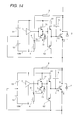
Embodiment 7
In a seventh embodiment, an arm shown in FIG. 3 consists of circuits which are shown in said FIG. 1, FIG. 4 through FIG. 13 and are connected in series. FIG. 14 shows an example. This embodiment suppresses dv/dt of the collector voltage of an IGBT 1 and also restrains overvoltage. Consequently, an electric potential between a collector and an emitter of the IGBT 1 connected in series can easily maintain equilibrium.

Claims (22)

What is claimed is:
1. A semiconductor electric power converter having an arm consisting of an IGBT, a capacitor connected between a collector and a gate of said IGBT, and a gate circuit connected to the gate of said IGBT for controlling the switching operation of said IGBT, wherein a plurality of said arms connected in series are connected in parallel and each midpoint of said arms connected in series is connected to a load,
said semiconductor electric power converter comprising a controllable impedance connected between the gate of said IGBT and a line of said gate circuit, wherein the impedance of said controllable impedance is decreased to discharge an electric charge stored in the gate when the gate voltage of said IGBT is higher than the gate voltage command value specified in response to the collector voltage of said IGBT.
2. A semiconductor electric power converter according to claim 1, wherein said arm consists of two IGBTs connected in series.
3. A semiconductor electric power converter having an arm consisting of an IGBT, a capacitor connected between a collector and a gate of said IGBT, and a gate circuit connected to the gate of said IGBT for controlling the switching operation of said IGBT, wherein a plurality of said arms connected in series are connected in parallel and each midpoint of said arms connected in series is connected to a load,
said semiconductor electric power converter comprising a controllable impedance connected between the gate of said IGBT and a negative potential line of said gate circuit, wherein the impedance between the gate of said IGBT and the negative potential line of said gate circuit is decreased when the gate voltage of said IGBT is higher than the gate voltage command value specified in response to the collector voltage of said IGBT.
4. A semiconductor electric power converter according to claim 3, wherein said arm consists of two IGBTs connected in series.
5. A semiconductor electric power converter having an arm consisting of an IGBT, a capacitor connected between a collector and a gate of said IGBT, and a gate circuit connected to the gate of said IGBT for controlling the switching operation of said IGBT, wherein a plurality of said arms connected in series are connected in parallel and each midpoint of said arms connected in series is connected to a load,
said semiconductor electric power converter comprising a controllable impedance connected between the gate and an emitter of said IGBT, wherein the impedance between the gate and the emitter of said IGBT is decreased when the gate voltage of said IGBT is higher than the gate voltage command value specified in response to the collector voltage of said IGBT.
6. A semiconductor electric power converter according to claim 5, wherein said arm consists of two IGBTs connected in series.
7. A semiconductor electric power converter having an arm consisting of an IGBT, a capacitor connected between a collector and a gate of said IGBT, and a gate circuit connected to the gate of said IGBT for controlling the switching operation of said IGBT, wherein a plurality of said arms connected in series are connected in parallel and each midpoint of said arms connected in series is connected to a load,
said semiconductor electric power converter comprising a controllable impedance connected between the gate of said IGBT and a negative potential line of said gate circuit and means for dividing the collector voltage of said IGB, wherein an electric charge stored in the gate of said IGBT is discharged when the gate potential is higher than the electric potential of the voltage dividing point executed by said voltage dividing means.
8. A semiconductor electric power converter according to claim 7, wherein an electric charge stored in the gate is discharged when the gate voltage is higher than the voltage of the voltage dividing point executed by said voltage dividing means.
9. A semiconductor electric power converter according to claim 7, wherein said arm consists of two IGBTs connected in series.
10. A semiconductor electric power converter having an arm consisting of an IGBT, a capacitor connected between a collector and a gate of said IGBT, and a gate circuit connected to the gate of said IGBT for controlling the switching operation of said IGBT, wherein a plurality of said arms connected in series are connected in parallel and each midpoint of said arms connected in series is connected to a load,
said semiconductor electric power converter comprising a controllable impedance connected between the gate of said IGBT and a negative potential line of said gate circuit and means for dividing the collector voltage of said IGB, wherein the impedance between the gate of said IGBT and the negative potential line of said gate circuit is decreased when the gate potential is higher than the electric potential of the voltage dividing point executed by said voltage dividing means.
11. A semiconductor electric power converter according to claim 10, wherein said arm consists of two IGBTs connected in series.
12. A semiconductor electric power converter according to claim 8, wherein said arm consists of two IGBTs connected in series.
13. A semiconductor electric power converter having an arm consisting of an IGBT, a capacitor connected between a collector and a gate of said IGBT, and a gate circuit connected to the gate of said IGBT for controlling the switching operation of said IGBT, wherein a plurality of said arms connected in series are connected in parallel and each midpoint of said arms connected in series is connected to a load,
said semiconductor electric power converter comprising means for dividing the collector voltage of said IGB, wherein a gate current is drawn to a negative potential line of said gate circuit by bypassing a gate resistor that restrains the gate current when the gate potential is higher than the electric potential of the voltage dividing point executed by said voltage dividing means.
14. A semiconductor electric power converter according to claim 13, wherein said arm consists of two IGBTs connected in series.
15. A semiconductor electric power converter having an arm consisting of an IGBT, a capacitor connected between a collector and a gate of said IGBT, and a gate circuit connected to the gate of said IGBT for controlling the switching operation of said IGBT, wherein a plurality of said arms connected in series are connected in parallel and each midpoint of said arms connected in series is connected to a load,
said semiconductor electric power converter comprising means for dividing the collector voltage of said IGB, wherein means for supplying a gate current to the gate is provided by bypassing a resistor that restrains charging current of the gate when the gate potential of said IGBT is lower than the electric potential of the voltage dividing point executed by said voltage dividing means, and a gate current is drawn to a negative potential line of said gate circuit by bypassing a resistor that restrains discharging current of the gate when the gate potential is higher than the electric potential of the voltage dividing point executed by said voltage dividing means.
16. A semiconductor electric power converter according to claim 15, wherein said arm consists of two IGBTs connected in series.
17. A semiconductor electric power converter having an arm consisting of an IGBT, a capacitor connected between a collector and a gate of said IGBT, and a gate circuit connected to the gate of said IGBT for controlling the switching operation of said IGBT, wherein a plurality of said arms connected in series are connected in parallel and each midpoint of said arms connected in series is connected to a load,
said semiconductor electric power converter comprising means for dividing the collector voltage of said IGB, wherein a circuit is provided for discharging an electric charge stored in the gate of said IGBT when the electric potential of the voltage dividing point executed by said voltage dividing means is higher than a prescribed value.
18. A semiconductor electric power converter according to claim 17, wherein said arm consists of two IGBTs connected in series.
19. A semiconductor electric power converter having an arm consisting of an IGBT, a capacitor connected between a collector and a gate of said IGBT, and a gate circuit connected to the gate of said IGBT for controlling the switching operation of said IGBT, wherein a plurality of said arms connected in series are connected in parallel and each midpoint of said arms connected in series is connected to a load,
said semiconductor electric power converter comprising a circuit for discharging an electric charge stored in the gate of said IGBT when a current flows from the gate of said IGBT to the direction for charging said capacitor.
20. A semiconductor electric power converter according to claim 19, wherein said arm consists of two IGBTs connected in series.
21. A semiconductor electric power converter having an arm consisting of an IGBT, a capacitor connected between a collector and a gate of said IGBT, and a gate circuit connected to the gate of said IGBT for controlling the switching operation of said IGBT, wherein a plurality of said arms connected in series are connected in parallel and each midpoint of said arms connected in series is connected to a load,
said semiconductor electric power converter comprising means for dividing the collector voltage of said IGB and means for comparing the voltage of the voltage dividing point executed by said voltage dividing means with the voltage for commanding switching operation of said IGBT and controlling the gate voltage to utilize a higher voltage.
22. A semiconductor electric power converter according to claim 21, wherein said arm consists of two IGBTs connected in series.
US09/972,981 2001-03-19 2001-10-10 Power conversion apparatus Expired - Lifetime US6490182B2 (en)

Applications Claiming Priority (3)

Application Number Priority Date Filing Date Title
JP2001077432A JP3812353B2 (en) 2001-03-19 2001-03-19 Semiconductor power converter
JP2001-077432 2001-03-19
JP2001-77432 2001-03-19

Publications (2)

Publication Number Publication Date
US20020131276A1 US20020131276A1 (en) 2002-09-19
US6490182B2 true US6490182B2 (en) 2002-12-03

Family

ID=18934192

Family Applications (1)

Application Number Title Priority Date Filing Date
US09/972,981 Expired - Lifetime US6490182B2 (en) 2001-03-19 2001-10-10 Power conversion apparatus

Country Status (2)

Country Link
US (1) US6490182B2 (en)
JP (1) JP3812353B2 (en)

Cited By (13)

* Cited by examiner, † Cited by third party
Publication number Priority date Publication date Assignee Title
JP2002281761A (en) * 2001-03-19 2002-09-27 Hitachi Ltd Semiconductor power converter
US20050111245A1 (en) * 2003-11-25 2005-05-26 Jih-Sheng Lai Multifunction hybrid intelligent universal transformer
US20050111246A1 (en) * 2003-11-25 2005-05-26 Jih-Sheng Lai Multilevel converter based intelligent universal transformer
US20070223258A1 (en) * 2003-11-25 2007-09-27 Jih-Sheng Lai Multilevel converters for intelligent high-voltage transformers
US20070230226A1 (en) * 2003-11-25 2007-10-04 Jih-Sheng Lai Multilevel intelligent universal auto-transformer
US20100008113A1 (en) * 2007-02-14 2010-01-14 Toyota Jidosha Kabushiki Kaisha Semiconductor power conversion device
US20100214197A1 (en) * 2009-02-26 2010-08-26 Hiroki Matsunaga Capacitive-load drive device and pdp display apparatus
US20110018593A1 (en) * 2007-05-21 2011-01-27 Advanced Analogic Technologies, Inc. MOSFET gate drive with reduced power loss
CN101860181B (en) * 2003-09-10 2012-01-11 东芝三菱电机产业系统株式会社 Gate drive circuit
US20120212861A1 (en) * 2011-02-18 2012-08-23 Paolo Menegoli Voltage spikes control for power converters
US20120313184A1 (en) * 2011-06-07 2012-12-13 Kabushiki Kaisha Toyota Jidoshokki Switching circuit
CN101707432B (en) * 2006-08-22 2013-01-02 株式会社日立制作所 Electric power switching device and abnormal test method thereof
US20150077075A1 (en) * 2013-09-17 2015-03-19 Dialog Semiconductor Gmbh Control Circuit for Multiple High Side Switches

Families Citing this family (15)

* Cited by examiner, † Cited by third party
Publication number Priority date Publication date Assignee Title
JP3891090B2 (en) * 2001-12-06 2007-03-07 株式会社デンソー Freewheeling diode and load driving circuit
DE10244749B3 (en) * 2002-09-25 2004-04-08 Siemens Ag Circuit arrangement for limiting overvoltages in power semiconductor components and method for controlling a power semiconductor component
DE10261911A1 (en) * 2002-12-30 2004-07-29 Volkswagen Ag Process for controlling the temperature of a catalytic converter and multi-cylinder engine with lambda-split exhaust gas cleaning system
JP2004228768A (en) 2003-01-21 2004-08-12 Toshiba Corp Gate driving circuit
JP4144541B2 (en) * 2004-03-19 2008-09-03 日産自動車株式会社 Driver circuit for voltage-driven semiconductor device
JP2006042564A (en) * 2004-07-30 2006-02-09 Tokyo Electric Power Co Inc:The Power switching circuit, power conversion device, and drive method of semiconductor switching element for power
FR2874767B1 (en) * 2004-08-27 2006-10-20 Schneider Toshiba Inverter DEVICE FOR CONTROLLING A POWER TRANSISTOR
JP4538047B2 (en) * 2007-12-25 2010-09-08 三菱電機株式会社 Failure detection device for power element
KR101261944B1 (en) * 2010-09-17 2013-05-09 기아자동차주식회사 Inverter control system
CN102290969B (en) * 2011-07-29 2013-07-24 清华大学 Voltage sharing control circuit for series operation of insulated gate bipolar transistors
US9203393B2 (en) * 2012-08-30 2015-12-01 Denso Corporation Semiconductor apparatus
EP3120446A4 (en) * 2014-03-20 2017-11-01 TM4 Inc. Gate driver controlling a collector to emitter voltage variation of an electronic switch and circuits including the gate driver
WO2017216974A1 (en) * 2016-06-17 2017-12-21 日産自動車株式会社 Drive device
CN110350770B (en) * 2019-06-20 2021-02-19 武汉大学 Auxiliary voltage source-based series IGBT voltage-sharing method and system
CN115378413B (en) * 2022-10-25 2023-01-24 成都市易冲半导体有限公司 Control circuit and control method

Citations (8)

* Cited by examiner, † Cited by third party
Publication number Priority date Publication date Assignee Title
JPH10248237A (en) 1997-03-04 1998-09-14 Toshiba Corp Power conversion apparatus
US5926012A (en) * 1996-09-20 1999-07-20 Fuji Electric Co., Ltd. Gate drive circuit in power converter with condition detection device
US5936387A (en) * 1996-10-17 1999-08-10 Fuji Electric Co., Ltd. Gate drive circuit for power converters that reduces surge voltages
US5946208A (en) * 1997-10-29 1999-08-31 Kabushiki Kaisha Meidensha Power converter
US6064578A (en) * 1998-02-02 2000-05-16 Kabushiki Kaisha Toshiba Power conversion system
US6169672B1 (en) * 1996-07-03 2001-01-02 Hitachi, Ltd. Power converter with clamping circuit
US6304472B1 (en) * 1999-05-14 2001-10-16 Hitachi, Ltd. Electric power converting system with integrator providing output indicative of current
US6373731B1 (en) * 2000-02-28 2002-04-16 Hitachi, Ltd. Surge voltage suppressed power inverter using a voltage driven switching element

Family Cites Families (7)

* Cited by examiner, † Cited by third party
Publication number Priority date Publication date Assignee Title
JPH0479758A (en) * 1990-07-19 1992-03-13 Fuji Electric Co Ltd Driving circuit of current sensing igbt
JP3141613B2 (en) * 1993-03-31 2001-03-05 株式会社日立製作所 Method and circuit for driving voltage-driven element
JP3424635B2 (en) * 1994-09-20 2003-07-07 株式会社日立製作所 Semiconductor device and power conversion device using the same
JP3373704B2 (en) * 1995-08-25 2003-02-04 三菱電機株式会社 Insulated gate transistor drive circuit
JP2000139071A (en) * 1998-11-02 2000-05-16 Fuji Electric Co Ltd Gate driving circuit for power converter
JP2000228883A (en) * 1999-02-04 2000-08-15 Fuji Electric Co Ltd Power converter
JP3812353B2 (en) * 2001-03-19 2006-08-23 株式会社日立製作所 Semiconductor power converter

Patent Citations (8)

* Cited by examiner, † Cited by third party
Publication number Priority date Publication date Assignee Title
US6169672B1 (en) * 1996-07-03 2001-01-02 Hitachi, Ltd. Power converter with clamping circuit
US5926012A (en) * 1996-09-20 1999-07-20 Fuji Electric Co., Ltd. Gate drive circuit in power converter with condition detection device
US5936387A (en) * 1996-10-17 1999-08-10 Fuji Electric Co., Ltd. Gate drive circuit for power converters that reduces surge voltages
JPH10248237A (en) 1997-03-04 1998-09-14 Toshiba Corp Power conversion apparatus
US5946208A (en) * 1997-10-29 1999-08-31 Kabushiki Kaisha Meidensha Power converter
US6064578A (en) * 1998-02-02 2000-05-16 Kabushiki Kaisha Toshiba Power conversion system
US6304472B1 (en) * 1999-05-14 2001-10-16 Hitachi, Ltd. Electric power converting system with integrator providing output indicative of current
US6373731B1 (en) * 2000-02-28 2002-04-16 Hitachi, Ltd. Surge voltage suppressed power inverter using a voltage driven switching element

Non-Patent Citations (1)

* Cited by examiner, † Cited by third party
Title
"Series Connection of High Voltage IGBT Modules" by M. Bruckmann et al., pp. 1067-1072 Jan. 1998.

Cited By (22)

* Cited by examiner, † Cited by third party
Publication number Priority date Publication date Assignee Title
JP2002281761A (en) * 2001-03-19 2002-09-27 Hitachi Ltd Semiconductor power converter
CN101860181B (en) * 2003-09-10 2012-01-11 东芝三菱电机产业系统株式会社 Gate drive circuit
US20070223258A1 (en) * 2003-11-25 2007-09-27 Jih-Sheng Lai Multilevel converters for intelligent high-voltage transformers
US6954366B2 (en) 2003-11-25 2005-10-11 Electric Power Research Institute Multifunction hybrid intelligent universal transformer
US20060028848A1 (en) * 2003-11-25 2006-02-09 Jih-Sheng Lai Multifunction hybrid intelligent universal transformer
US7050311B2 (en) 2003-11-25 2006-05-23 Electric Power Research Institute, Inc. Multilevel converter based intelligent universal transformer
US20050111246A1 (en) * 2003-11-25 2005-05-26 Jih-Sheng Lai Multilevel converter based intelligent universal transformer
US20070230226A1 (en) * 2003-11-25 2007-10-04 Jih-Sheng Lai Multilevel intelligent universal auto-transformer
US20050111245A1 (en) * 2003-11-25 2005-05-26 Jih-Sheng Lai Multifunction hybrid intelligent universal transformer
CN101707432B (en) * 2006-08-22 2013-01-02 株式会社日立制作所 Electric power switching device and abnormal test method thereof
US20100008113A1 (en) * 2007-02-14 2010-01-14 Toyota Jidosha Kabushiki Kaisha Semiconductor power conversion device
DE112008000399B4 (en) 2007-02-14 2018-05-30 Toyota Jidosha Kabushiki Kaisha Semiconductor power conversion device
US8050064B2 (en) * 2007-02-14 2011-11-01 Toyota Jidosha Kabushiki Kaisha Semiconductor power conversion device
US20110018593A1 (en) * 2007-05-21 2011-01-27 Advanced Analogic Technologies, Inc. MOSFET gate drive with reduced power loss
US7994827B2 (en) * 2007-05-21 2011-08-09 Advanced Analogic Technologies, Inc. MOSFET gate drive with reduced power loss
US20100214197A1 (en) * 2009-02-26 2010-08-26 Hiroki Matsunaga Capacitive-load drive device and pdp display apparatus
US20120212861A1 (en) * 2011-02-18 2012-08-23 Paolo Menegoli Voltage spikes control for power converters
US8441770B2 (en) * 2011-02-18 2013-05-14 ETA Semiconductor Inc Voltage spikes control for power converters
US20120313184A1 (en) * 2011-06-07 2012-12-13 Kabushiki Kaisha Toyota Jidoshokki Switching circuit
US9083333B2 (en) * 2011-06-07 2015-07-14 Kabushiki Kaisha Toyota Jidoshokki Switching circuit
US20150077075A1 (en) * 2013-09-17 2015-03-19 Dialog Semiconductor Gmbh Control Circuit for Multiple High Side Switches
US9407132B2 (en) * 2013-09-17 2016-08-02 Dialog Semiconductor Gmbh Control circuit for multiple high side switches

Also Published As

Publication number Publication date
JP3812353B2 (en) 2006-08-23
JP2002281761A (en) 2002-09-27
US20020131276A1 (en) 2002-09-19

Similar Documents

Publication Publication Date Title
US6490182B2 (en) Power conversion apparatus
US11139808B2 (en) Semiconductor device and power conversion system
JP3462032B2 (en) Power converter
US9461640B2 (en) Switching element drive circuit, power module, and automobile
US6744644B2 (en) Soft-start of DC link capacitors for power electronics and drive systems
US6392908B2 (en) Method and apparatus for driving a semiconductor element
JP3193827B2 (en) Semiconductor power module and power converter
US7368972B2 (en) Power transistor control device
US7940503B2 (en) Power semiconductor arrangement including conditional active clamping
US20140307495A1 (en) Driver for target switching element and control system for machine using the same
US20030206423A1 (en) 3-level inverter apparatus
US20100321847A1 (en) Semiconductor power conversion apparatus
WO2006052032A1 (en) Power converter
JP5206198B2 (en) Driving circuit for power conversion circuit
CN113056864B (en) power conversion device
US6727516B2 (en) Semiconductor power conversion apparatus
CN111224536B (en) Driving device of anti-Miller effect power module and electronic equipment
JP5098872B2 (en) Driving circuit for power conversion circuit
JP6664311B2 (en) Drive system and power converter
US20190293725A1 (en) Voltage detection device
KR19990006822A (en) Controller of charge generator
JPH10209832A (en) Semiconductor switch circuit
WO2022153521A1 (en) Semiconductor power conversion device
US20220149839A1 (en) Semiconductor device
US20230308008A1 (en) Semiconductor device

Legal Events

Date Code Title Description
AS Assignment

Owner name: HITACHI, LTD., JAPAN

Free format text: ASSIGNMENT OF ASSIGNORS INTEREST;ASSIGNORS:KATOH, SHUJI;SAKAI, HIROMITUS;UEDA, SHIGETA;AND OTHERS;REEL/FRAME:012253/0141

Effective date: 20010910

STCF Information on status: patent grant

Free format text: PATENTED CASE

FEPP Fee payment procedure

Free format text: PAYOR NUMBER ASSIGNED (ORIGINAL EVENT CODE: ASPN); ENTITY STATUS OF PATENT OWNER: LARGE ENTITY

FPAY Fee payment

Year of fee payment: 4

FEPP Fee payment procedure

Free format text: PAYER NUMBER DE-ASSIGNED (ORIGINAL EVENT CODE: RMPN); ENTITY STATUS OF PATENT OWNER: LARGE ENTITY

FEPP Fee payment procedure

Free format text: PAYOR NUMBER ASSIGNED (ORIGINAL EVENT CODE: ASPN); ENTITY STATUS OF PATENT OWNER: LARGE ENTITY

FPAY Fee payment

Year of fee payment: 8

FPAY Fee payment

Year of fee payment: 12

AS Assignment

Owner name: HITACHI INDUSTRIAL PRODUCTS, LTD., JAPAN

Free format text: MERGER;ASSIGNOR:HITACHI, LTD.;REEL/FRAME:051758/0373

Effective date: 20190401