US6492069B1 - Method for forming an attenuated phase-shifting mask - Google Patents

Method for forming an attenuated phase-shifting mask Download PDF

Info

Publication number
US6492069B1
US6492069B1 US09/534,171 US53417100A US6492069B1 US 6492069 B1 US6492069 B1 US 6492069B1 US 53417100 A US53417100 A US 53417100A US 6492069 B1 US6492069 B1 US 6492069B1
Authority
US
United States
Prior art keywords
layer
photoresist layer
shifting
phase
opaque
Prior art date
Legal status (The legal status is an assumption and is not a legal conclusion. Google has not performed a legal analysis and makes no representation as to the accuracy of the status listed.)
Expired - Lifetime
Application number
US09/534,171
Inventor
Ching-Liang Wu
Yueh-Lin Chou
Jen-Hui Tseng
Current Assignee (The listed assignees may be inaccurate. Google has not performed a legal analysis and makes no representation or warranty as to the accuracy of the list.)
Taiwan Semiconductor Manufacturing Co TSMC Ltd
Original Assignee
Worldwide Semiconductor Manufacturing Corp
Priority date (The priority date is an assumption and is not a legal conclusion. Google has not performed a legal analysis and makes no representation as to the accuracy of the date listed.)
Filing date
Publication date
Application filed by Worldwide Semiconductor Manufacturing Corp filed Critical Worldwide Semiconductor Manufacturing Corp
Assigned to WORLDWIDE SEMICONDUCTOR MANUFACTURING CORP. reassignment WORLDWIDE SEMICONDUCTOR MANUFACTURING CORP. ASSIGNMENT OF ASSIGNORS INTEREST (SEE DOCUMENT FOR DETAILS). Assignors: TSENG, JEN-HUI, CHOU, YUEH-LIN, WU, CHING-LIANG
Assigned to TAIWAN SEMICONDUCTOR MANUFACTURING CO., LTD. reassignment TAIWAN SEMICONDUCTOR MANUFACTURING CO., LTD. ASSIGNMENT OF ASSIGNORS INTEREST (SEE DOCUMENT FOR DETAILS). Assignors: WORLDWIDE SEMICONDUCTOR MANUFACTURING CORP.
Application granted granted Critical
Publication of US6492069B1 publication Critical patent/US6492069B1/en
Anticipated expiration legal-status Critical
Expired - Lifetime legal-status Critical Current

Links

Images

Classifications

    • GPHYSICS
    • G03PHOTOGRAPHY; CINEMATOGRAPHY; ANALOGOUS TECHNIQUES USING WAVES OTHER THAN OPTICAL WAVES; ELECTROGRAPHY; HOLOGRAPHY
    • G03FPHOTOMECHANICAL PRODUCTION OF TEXTURED OR PATTERNED SURFACES, e.g. FOR PRINTING, FOR PROCESSING OF SEMICONDUCTOR DEVICES; MATERIALS THEREFOR; ORIGINALS THEREFOR; APPARATUS SPECIALLY ADAPTED THEREFOR
    • G03F1/00Originals for photomechanical production of textured or patterned surfaces, e.g., masks, photo-masks, reticles; Mask blanks or pellicles therefor; Containers specially adapted therefor; Preparation thereof
    • G03F1/26Phase shift masks [PSM]; PSM blanks; Preparation thereof
    • G03F1/32Attenuating PSM [att-PSM], e.g. halftone PSM or PSM having semi-transparent phase shift portion; Preparation thereof

Landscapes

  • Physics & Mathematics (AREA)
  • General Physics & Mathematics (AREA)
  • Preparing Plates And Mask In Photomechanical Process (AREA)
  • Exposure And Positioning Against Photoresist Photosensitive Materials (AREA)

Abstract

This invention discloses a method for forming an attenuated phase-shifting mask, including following steps. A transparent plate is provided, on which a phase-shifting layer, opaque layer, and undeveloped photoresist layer being stacked on the transparent plate successively. A first part of the photoresist layer is removed until exposing a first region of the opaque layer. The first region of the opaque layer is removed for exposing parts of the phase-shifting layer. A second part of the photoresist layer is removed for exposing a second region of the opaque layer. The exposed phase-shifting layer is then etched by employing the opaque layer as an etching mask. Then the exposed opaque layer and photoresist layer are successively remove, thus forming a complete attenuated phase-shifting mask.

Description

FIELD OF THE INVENTION
This invention relates to a method of forming a mask for photolithography, and more particularly to a method for forming an attenuated phase-shifting mask (PSM).
BACKGROUND OF THE INVENTION
An attenuated phase-shifting mask (PSM), a widely used mask in photolithography, is mainly fabricated by coating a phase-shifting layer upon on a transparent plate, thus to interfere the phase of light incident through the transparent plate for providing a better exposure accuracy during the photolithography. As a result of the better exposure accuracy, patterns of attenuated phase-shifting mask would be transformed onto chips more accurate than those of conventional mask do. Typically, a stepper, a machine for projecting rays through masks onto chips during photolithography, identifies and locates a mask by detecting reflected ray form bar codes and position marks at edges of the mask. However, the stepper doesn't always successfully identify and locate attenuated phase-shifting masks, since a great amount of incident light would pass through the phase-shifting layer so as provide insufficient amount of reflected ray for identifying and locating them. Moreover, patterns of chips transformed form edges of the phase-shifting layer might be exposed in overlap after the use of several attenuated phase-shifting masks. The photoresist layer of those patterns will undesirably lose due to the overlapped exposures, thereby damaging the accuracy of patterns of chips.
For overcoming the above mentioned problems of applying attenuated phase-shifting mask, many semiconductor manufacturers coat an opaque layer around its edges for facilitating steppers to identify and locate the attenuated phase-shifting mask by the reflected ray from the opaque layer at the edges. Referring to FIG. 1, an attenuated phase-shifting mask 34 is coated with a opaque layer 38 around the central image field 36, which includes patterns formed by a phase-shifting layer coated on a transparent plate. Due to the opaque layer 38, a stepper is able to detect the reflected ray from the bar code 40 and position marks 42 to identify and locate the attenuated phase-shifting mask 34.
Through FIG. 2 to FIG. 8, a conventional process for fabricating an attenuated phase-shifting mask with the opaque layer in semiconductor manufacturer's plant is shown. FIG. 2 shows a cross-sectional view of an attenuated phase-shifting mask 44 provided by mask vendors. The attenuated phase-shifting layer 44 is formed by successively coating a phase-shifting layer 48, opaque layer 50, and first photoresist layer 52 on a transparent plate 46. In order to form patterns on the attenuated phase-shifting mask 44, the first photoresist layer is defined as shown in FIG. 3 by exposure and development. Referring to FIG. 3, parts of the opaque layer 50 are then stripped through a conventional etching process by employing the photoresist layer 52 as an etching mask. Then the photoresist layer 52 is totally stripped thus to shape the cross-sectional view of FIG. 4. Using the opaque layer 50 as an etching mask, parts of the phase-shifting layer 48 are removed until exposing the surface of transparent plate 46, as shown in FIG. 5.
Referring to FIG. 6, a second photoresist layer 54 is blanketed over the transparent plate 46. Through steps of exposure and development, the second photoresist layer 54 is partially removed as the cross-sectional view shown in FIG. 7. Parts of the opaque layer 50 exposed out of the second photoresist layer 54 are stripped through an etching process by employing the second photoresist layer 54 as an etching mask, then removing the second photoresist layer 54 to complete the attenuated phase-shifting mask 44, as shown in FIG. 8. As a result of the opaque layer 50 around upon the phase-shifting layer 48 and transparent layer 46, the stepper may correctly identify and located the attenuated phase-shifting mask 44 by detecting reflected rays from the opaque layer 50.
Although this conventional process enables semiconductor manufacturers to fabricate an attenuated phase-shifting mask with an opaque layer, it exists some shortcomings. This conventional process is much complicated, since it needs to an extra photoresist layer, namely the aforementioned second photoresist layer. For forming the extra photoresist layer, the semiconductor manufacturers need to coat second photoresist layer on a original mask, which already has a first photoresist layer provided by mask vendors. Because of the square shape of mask, it's hard to coat the second photoresist layer uniformly as its corners by semiconductor manufacturers themselves. Therefore, under this conventional process, the semiconductor manufacturers suffer low yield rates and high costs from it.
In brief, for forming an opaque layer around an attenuated phase-shifting mask as well as avoiding the low yield and cost due to the conventional process, there is huge need to improve the conventional process to overcome the above problems.
SUMMARY OF THE INVENTION
An objective of this invention is to provide semiconductor manufacturers a simplified method to from an attenuated phase-shifting mask.
This invention discloses a method for forming an attenuated phase-shifting mask, including following steps. A transparent plate is provided, on which a phase-shifting layer, opaque layer, and undeveloped photoresist layer being stacked on the transparent plate successively. A first part of the photoresist layer is removed until exposing a first region of the opaque layer through exposure and development processes. The first region of the opaque layer is removed for exposing parts of the phase-shifting layer. A solidified thin surface of the photoresist layer is stripped by low-energy plasma treatment. A second part of the photoresist layer is removed for exposing a second region of the opaque layer through exposure and development processes. The exposed phase-shifting layer is then etched by employing the opaque layer as an etching mask. Then the exposed opaque layer and photoresist layer are successively remove, thus forming a complete attenuated phase-shifting mask.
BRIEF DESCRIPTION OF THE DRAWINGS
FIG. 1 is a top view of an attenuated phase-shifting mask;
FIG. 2 is a cross-sectional view of an original phase-shifting mask provided by mask venders, in accordance with prior arts;
FIG. 3 is a cross-sectional view of etching an opaque layer by employing a first photoresist layer as an etching mask, in accordance with prior arts;
FIG. 4 is a cross-sectional view of stripping the first photoresist layer, in accordance with prior arts;
FIG. 5 is a cross-sectional view of etching a phase-shifting layer by employing the opaque layer as an etching mask, in accordance with prior arts;
FIG. 6 is a cross-sectional view of coating a second photoresist layer on the original phase-shifting mask, in accordance with prior arts;
FIG. 7 is a cross-sectional view of removing parts of the second photoresist layer, in accordance with prior arts;
FIG. 8 is a cross-sectional view showing a complete attenuated phase-shifting mask, in accordance with prior arts;
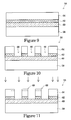
FIG. 9 is a cross-sectional view of an original attenuated phase-shifting mask provided by mask venders, in this invention;
FIG. 10 is a cross-sectional view of etching an opaque layer by employing a photoresist layer as an etching mask, in this invention;
FIG. 11 is a cross-sectional view of treating a surface of the photoresist layer, in this invention;
FIG. 12 is a cross-sectional view of removing parts of the photoresist layer, in this invention;
FIG. 13 is a cross-sectional view of etching the phase-shifting layer by employing the opaque layer as an etching layer, in this invention;
FIG. 14 is a cross-sectional view of removing the photoresist layer and parts of the opaque layer to form a complete attenuated phase-shifting mask, in this invention.
DETAILED DESCRIPTION OF THE PREFERRED EMBODIMENT
This invention proposes a method for forming an attenuated phase-shifting mask with an opaque layer around it form an original mask the mask venders provide. This method uses only one photoresist layer, which is inherently provided by mask venders, to form an opaque layer by a step of treating the surface of the photoresist layer. By avoiding extra exposure and development, this method overcomes the problems of low yield and high cost in the conventional process. For illustrating the invention clearly, a preferred embodiment is presented in following paragraphs in combination with FIG. 9 through FIG. 14.
FIG. 9 shows a cross-sectional view of an original attenuated phase-shifting mask 56 provided by mask vendors. The attenuated phase-shifting mask 56 is substantially formed by successively coating a phase-shifting layer 60, opaque layer 62, and photoresist layer 64 on a transparent plate 58. In this embodiment, the transparent plate 58 is made of quartz or glass in a thickness about 250 mil. The phase-shifting layer 60 is used to adjust phases of incident rays through the attenuated phase-shifting mask 56, thereby transforming its patterns to chips in accuracy. In this embodiment, the phase-shifting layer 60 is made of MoSiON in a thickness about 1350 A. As for the opaque layer 62, its function is for serving as a reflection region around the attenuated phase-shifting mask 56 to facilitate steppers to identify and locate the mask. In this preferred embodiment, the opaque layer is made of chromium in a thickness about 1050 A.
Referring to FIG. 10, the photoresist layer 64 is firstly exposed by light to define a first region 66. The first region 66 is then removed until exposing parts of the surface of opaque layer 60 by dipping the attenuated phase-shifting mask 56 into developer solution according to conventional development process. The exposed parts of opaque layer 62 are then removed until exposing parts of the phase-shifting layer 60 through a wet etching process by employing the photoresist layer 64 as an etching mask. In this embodiment, the opaque layer 62, i.e. chromium layer, is removed by (NH4)Ce(NO3)6 through a conventional wet etching process, but could also be removed by Cl2 plasma through a conventional dry etching process as an alternative.
Referring to FIG. 11, the surface of photoresist layer 64 is treated by low-energy plasma to strip a thin layer form its top surface for further redefining the photoresist layer 64. After the photoresist layer 64 has been defined through the forgoing exposure and development, there is a thin solidified layer atop the photoresist layer 64. For recycling and redefining the photoresist layer 64, the solidified layer must be removed, and the second region 68 of the photoresist layer 64 could be removed by secondly exposing and developing the attenuated phase-shifting mask 56, as shown in FIG. 12. In this preferred embodiment, the solidified layer of photoresist layer 64 can be stripped to an approximate thickness between about 100˜200 angstroms by relatively low-energy O2 plasma treatment.
Referring to FIG. 13, parts of the phase-shifting layer 60 exposed out of the opaque layer 62 are removed until exposing part surfaces of the transparent plate 58 through an etching process by employing the opaque layer 62 as an etching mask. For adjust phases of incident rays through the attenuated phase-shifting mask 56, the exposed surfaces of transparent plate 58 are further slightly etched into it. In this embodiment, the phase-shifting layer 60, i.e. MoSiON layer, can be removed by CF4 plasma through a dry etching process, and the transparent plate, such as quartz plate or glass plate, can be also etched by CF4 plasma through a dry etching process. After the etching of transparent plate 58, the exposed opaque layer 62, namely the parts of the second region 68, and the photoresist layer 64 are successively stripped through conventional wet etching or dry etching process, thereby forming a complete attenuated phase-shifting mask 56 as shown in FIG. 14.
This invention simplifies the conventional process of forming attenuated phase-shifting mask, which needs complicated steps to form two photoresist layers, thereby raising the yield rates as well as decreasing the cost. In realistic applications, by this invention, semiconductor manufacturers are able to avoid to coat photoresist layers by themselves. Thus, the problems due to coating masks with photoresist materials, such as uneven contour of photoresist layer at corners of the mask, are overcome because this invention enables semiconductor manufacturers bypass coating photoresist materials by themselves.
As is understood by a person skilled in the art, the foregoing preferred embodiments of the present invention that are illustrated of the present invention rather than limiting of the present invention. It is intended to cover various modifications and similar arrangements included within the spirit and scope of the appended claims, the scope of which should be accorded the broadest interpretation so as to encompass all such modifications and similar structure.

Claims (18)

What is claimed is:
1. A method for forming an attenuated phase-shifting mask utilizing a single undeveloped photoresist layer, which comprises:
providing a transparent plate, a phase-shifting layer, an opaque layer, and an undeveloped photoresist layer being stacked on the transparent plate successively;
removing a first part of the photoresist layer for exposing a first region of the opaque layer;
removing the first region of the opaque layer for partially exposing the phase-shifting layer;
then removing a second part of the photoresist layer for exposing a second region of the opaque layer;
etching the phase-shifting layer until exposing a surface of the transparent plate by employing the opaque layer as an etching mask;
removing the second region of the opaque layer exposed out of the remaining photoresist layer; and then
removing the remaining photoresist layer for forming the attenuated phase-shifting layer with the opaque layer partially coated on the transparent plate.
2. The method of claim 1, further comprising the following steps before removing a first part of the photoresist layer:
exposing the photoresist layer for defining the first region; and then
first developing the photoresist layer.
3. The method of claim 2, further comprising the following steps before removing the second part of the photoresist layer:
treating a surface of the photoresist layer for removing a solidified layer atop the photoresist layer through the step of first developing;
exposing the photoresist layer; and then
developing the photoresist layer.
4. The method of claim 3, wherein the step of treating a surface is a dry etching process by O2 plasma.
5. The method of claim 3, wherein the solidified layer has a thickness in between about 100˜200 angstroms.
6. The method of claim 1, wherein, before removing the second region of the opaque layer exposed out of the remaining photoresist layer, further comprising a step of etching the transparent plate exposed out of the opaque layer for adjusting a shifting phase of an incident light through the transparent plate.
7. The method of claim 1, wherein the opaque layer is chromium, which is removed by (NH4)Ce(NO3)6 through a wet etching process.
8. The method of claim 1, wherein the phase-shifting layer is MoSiON.
9. The method of claim 1, wherein the MoSiON is removed by Cl2 plasma through a dry etching process.
10. The method of claim 1, wherein the opaque layer is partially formed around the attenuated phase-shifting mask to facilitate a stepper for identifying and locating the attenuated phase-shifting mask after the step of removing the remaining photoresist layer.
11. A method for forming an attenuated phase-shifting mask utilizing a single undeveloped photoresist layer, which comprises:
providing a transparent plate, a phase-shifting layer, an opaque layer, and an undeveloped photoresist layer being stacked on the transparent plate successively;
first exposing the photoresist layer for defining a first region of the opaque layer;
first developing the photoresist layer;
removing the first region of the opaque layer for partially exposing the phase-shifting layer;
treating a surface of the photoresist layer for removing a solidified layer atop the photoresist layer through the step of first developing the photoresist layer;
secondly exposing the photoresist layer;
secondly developing the photoresist layer for exposing a second region of the opaque layer;
etching the phase-shifting layer until exposing a surface of the transparent plate by employing the opaque layer as an etching mask;
removing the second region of the opaque layer exposed out of the photoresist layer; and
thirdly removing the remaining photoresist layer for forming the attenuated phase-shifting layer with the opaque layer partially coated on the transparent plate.
12. The method of claim 11, wherein the step of treating a surface is a dry etching process by O2 plasma.
13. The method of claim 11, wherein the solidified layer has a thickness in between about 100˜200 angstroms.
14. The method of claim 11, before removing the second region of the opaque layer exposed out of the photoresist layer further comprising a step of etching the transparent plate exposed out of the opaque layer for adjusting a shifting phase of an incident light through the transparent plate.
15. The method of claim 11, wherein the opaque layer is chromium, which is removed by (NH4)Ce(NO3)6 through a wet etching process.
16. The method of claim 11, wherein the phase-shifting layer is MoSiON.
17. The method of claim 16, wherein the MoSiON is removed by Cl2 plasma through a dry etching process.
18. The method of claim 11, wherein the opaque layer is partially formed around the attenuated phase-shifting mask to facilitate a stepper for identifying and locating the attenuated phase-shifting mask after the step of thirdly removing.
US09/534,171 2000-03-10 2000-03-24 Method for forming an attenuated phase-shifting mask Expired - Lifetime US6492069B1 (en)

Applications Claiming Priority (2)

Application Number Priority Date Filing Date Title
TW89104447A 2000-03-10
TW089104447A TW452678B (en) 2000-03-10 2000-03-10 Method of forming attenuated phase shifting mask

Publications (1)

Publication Number Publication Date
US6492069B1 true US6492069B1 (en) 2002-12-10

Family

ID=21659055

Family Applications (1)

Application Number Title Priority Date Filing Date
US09/534,171 Expired - Lifetime US6492069B1 (en) 2000-03-10 2000-03-24 Method for forming an attenuated phase-shifting mask

Country Status (2)

Country Link
US (1) US6492069B1 (en)
TW (1) TW452678B (en)

Cited By (5)

* Cited by examiner, † Cited by third party
Publication number Priority date Publication date Assignee Title
US6566280B1 (en) * 2002-08-26 2003-05-20 Intel Corporation Forming polymer features on a substrate
US20040185348A1 (en) * 2003-03-18 2004-09-23 Progler Christopher J. Alternating aperture phase shift photomask having light absorption layer
US20050097502A1 (en) * 2003-10-31 2005-05-05 Frost Rex K. Accommodating diffraction in the printing of features on a substrate
US20070003844A1 (en) * 2003-12-10 2007-01-04 Rasmussen Robert T Method for adjusting dimensions of photomask features
CN111427188A (en) * 2020-04-23 2020-07-17 昆山龙腾光电股份有限公司 Color filter substrate and manufacturing method thereof

Citations (1)

* Cited by examiner, † Cited by third party
Publication number Priority date Publication date Assignee Title
US5589303A (en) * 1994-12-30 1996-12-31 Lucent Technologies Inc. Self-aligned opaque regions for attenuating phase-shifting masks

Patent Citations (1)

* Cited by examiner, † Cited by third party
Publication number Priority date Publication date Assignee Title
US5589303A (en) * 1994-12-30 1996-12-31 Lucent Technologies Inc. Self-aligned opaque regions for attenuating phase-shifting masks

Cited By (12)

* Cited by examiner, † Cited by third party
Publication number Priority date Publication date Assignee Title
US6566280B1 (en) * 2002-08-26 2003-05-20 Intel Corporation Forming polymer features on a substrate
US20040185348A1 (en) * 2003-03-18 2004-09-23 Progler Christopher J. Alternating aperture phase shift photomask having light absorption layer
WO2004083960A2 (en) * 2003-03-18 2004-09-30 Photronics, Inc. Alternating aperture phase shift photomask having light absorption layer
WO2004083960A3 (en) * 2003-03-18 2005-02-03 Photronics Inc Alternating aperture phase shift photomask having light absorption layer
US20050170288A1 (en) * 2003-03-18 2005-08-04 Photronics, Inc. Alternating aperture phase shift photomask having light absorption layer
US6933084B2 (en) * 2003-03-18 2005-08-23 Photronics, Inc. Alternating aperture phase shift photomask having light absorption layer
US7344824B2 (en) 2003-03-18 2008-03-18 Photronics, Inc. Alternating aperture phase shift photomask having light absorption layer
US20050097502A1 (en) * 2003-10-31 2005-05-05 Frost Rex K. Accommodating diffraction in the printing of features on a substrate
US7288344B2 (en) 2003-10-31 2007-10-30 Intel Corporation Accommodating diffraction in the printing of features on a substrate
US20070003844A1 (en) * 2003-12-10 2007-01-04 Rasmussen Robert T Method for adjusting dimensions of photomask features
US7749663B2 (en) * 2003-12-10 2010-07-06 Micron Technology, Inc. Method for adjusting dimensions of photomask features
CN111427188A (en) * 2020-04-23 2020-07-17 昆山龙腾光电股份有限公司 Color filter substrate and manufacturing method thereof

Also Published As

Publication number Publication date
TW452678B (en) 2001-09-01

Similar Documents

Publication Publication Date Title
TW511149B (en) Photomask and method for manufacturing the same
US7494749B2 (en) Photolithography using interdependent binary masks
US6492069B1 (en) Method for forming an attenuated phase-shifting mask
JP2003524201A (en) Novel chromeless alternating reticle for manufacturing semiconductor device morphology
JPH0387014A (en) Optimizing method for photoresist contrast
EP0517382B1 (en) Method of forming resist pattern on a semiconductor substrate by light exposure
JPH06250376A (en) Phase shift mask and production of phase shift mask
TW587202B (en) Method of repairing attenuate phase shift mask
US20030039892A1 (en) Method of optical proximity correction
KR100350762B1 (en) Formation method of micropattern
KR0128833B1 (en) Micro-patterning method of semiconductor device
JP3091886B2 (en) Method of forming resist pattern
JPH0431858A (en) Manufacture of mask
US6306549B1 (en) Method for manufacturing EAPSM-type masks used to produce integrated circuits
US5932376A (en) Phase-shifting mask structure
JPS6156349A (en) Manufacture of photomask
KR920003811B1 (en) Exposure method on photoresist
US6531264B1 (en) Integrated circuit manufacture
JPH0547623A (en) Formation of resist mask pattern in optical exposure
KR100596276B1 (en) Method for forming photoresist pattern
KR100284026B1 (en) Fine pattern formation method using sillation
US7008729B2 (en) Method for fabricating phase mask of photolithography process
KR20080106696A (en) A manufacturing method using a top coating pattern as a supplementary etching mask
KR970016782A (en) Photomask and its manufacturing method
KR980010603A (en) Photomask manufacturing method

Legal Events

Date Code Title Description
AS Assignment

Owner name: WORLDWIDE SEMICONDUCTOR MANUFACTURING CORP., TAIWA

Free format text: ASSIGNMENT OF ASSIGNORS INTEREST;ASSIGNORS:WU, CHING-LIANG;CHOU, YUEH-LIN;TSENG, JEN-HUI;REEL/FRAME:010647/0362;SIGNING DATES FROM 19991220 TO 20000308

AS Assignment

Owner name: TAIWAN SEMICONDUCTOR MANUFACTURING CO., LTD., TAIW

Free format text: ASSIGNMENT OF ASSIGNORS INTEREST;ASSIGNOR:WORLDWIDE SEMICONDUCTOR MANUFACTURING CORP.;REEL/FRAME:010958/0881

Effective date: 20000601

STCF Information on status: patent grant

Free format text: PATENTED CASE

FPAY Fee payment

Year of fee payment: 4

FPAY Fee payment

Year of fee payment: 8

FPAY Fee payment

Year of fee payment: 12