US6496012B1 - Apparatus and method for detecting a short circuit in a lighting system - Google Patents

Apparatus and method for detecting a short circuit in a lighting system Download PDF

Info

Publication number
US6496012B1
US6496012B1 US09/667,450 US66745000A US6496012B1 US 6496012 B1 US6496012 B1 US 6496012B1 US 66745000 A US66745000 A US 66745000A US 6496012 B1 US6496012 B1 US 6496012B1
Authority
US
United States
Prior art keywords
voltage
current
phase
current signals
input
Prior art date
Legal status (The legal status is an assumption and is not a legal conclusion. Google has not performed a legal analysis and makes no representation as to the accuracy of the status listed.)
Expired - Fee Related, expires
Application number
US09/667,450
Inventor
Da Feng Weng
Chin Chang
Current Assignee (The listed assignees may be inaccurate. Google has not performed a legal analysis and makes no representation or warranty as to the accuracy of the list.)
Koninklijke Philips NV
Original Assignee
Koninklijke Philips Electronics NV
Priority date (The priority date is an assumption and is not a legal conclusion. Google has not performed a legal analysis and makes no representation as to the accuracy of the date listed.)
Filing date
Publication date
Application filed by Koninklijke Philips Electronics NV filed Critical Koninklijke Philips Electronics NV
Priority to US09/667,450 priority Critical patent/US6496012B1/en
Assigned to PHILIPS ELECTRONICS NORTH AMERICA CORPORATION reassignment PHILIPS ELECTRONICS NORTH AMERICA CORPORATION ASSIGNMENT OF ASSIGNORS INTEREST (SEE DOCUMENT FOR DETAILS). Assignors: CHANG, CHIN, WENG, DA FENG
Priority to PCT/EP2001/010583 priority patent/WO2002025791A2/en
Priority to EP01980379A priority patent/EP1234365A2/en
Priority to CN01802826.8A priority patent/CN1394373A/en
Priority to JP2002528893A priority patent/JP2004509597A/en
Assigned to KONINKLIJKE PHILIPS ELECTRONICS N.V. reassignment KONINKLIJKE PHILIPS ELECTRONICS N.V. ASSIGNMENT OF ASSIGNORS INTEREST (SEE DOCUMENT FOR DETAILS). Assignors: PHILIPS ELECTRONICS NORTH AMERICA CORPORATION
Application granted granted Critical
Publication of US6496012B1 publication Critical patent/US6496012B1/en
Adjusted expiration legal-status Critical
Expired - Fee Related legal-status Critical Current

Links

Images

Classifications

    • HELECTRICITY
    • H02GENERATION; CONVERSION OR DISTRIBUTION OF ELECTRIC POWER
    • H02HEMERGENCY PROTECTIVE CIRCUIT ARRANGEMENTS
    • H02H3/00Emergency protective circuit arrangements for automatic disconnection directly responsive to an undesired change from normal electric working condition with or without subsequent reconnection ; integrated protection
    • H02H3/38Emergency protective circuit arrangements for automatic disconnection directly responsive to an undesired change from normal electric working condition with or without subsequent reconnection ; integrated protection responsive to both voltage and current; responsive to phase angle between voltage and current
    • H02H3/382Emergency protective circuit arrangements for automatic disconnection directly responsive to an undesired change from normal electric working condition with or without subsequent reconnection ; integrated protection responsive to both voltage and current; responsive to phase angle between voltage and current involving phase comparison between current and voltage or between values derived from current and voltage
    • HELECTRICITY
    • H02GENERATION; CONVERSION OR DISTRIBUTION OF ELECTRIC POWER
    • H02HEMERGENCY PROTECTIVE CIRCUIT ARRANGEMENTS
    • H02H7/00Emergency protective circuit arrangements specially adapted for specific types of electric machines or apparatus or for sectionalised protection of cable or line systems, and effecting automatic switching in the event of an undesired change from normal working conditions
    • H02H7/04Emergency protective circuit arrangements specially adapted for specific types of electric machines or apparatus or for sectionalised protection of cable or line systems, and effecting automatic switching in the event of an undesired change from normal working conditions for transformers
    • HELECTRICITY
    • H05ELECTRIC TECHNIQUES NOT OTHERWISE PROVIDED FOR
    • H05BELECTRIC HEATING; ELECTRIC LIGHT SOURCES NOT OTHERWISE PROVIDED FOR; CIRCUIT ARRANGEMENTS FOR ELECTRIC LIGHT SOURCES, IN GENERAL
    • H05B41/00Circuit arrangements or apparatus for igniting or operating discharge lamps
    • H05B41/14Circuit arrangements
    • H05B41/26Circuit arrangements in which the lamp is fed by power derived from dc by means of a converter, e.g. by high-voltage dc
    • H05B41/28Circuit arrangements in which the lamp is fed by power derived from dc by means of a converter, e.g. by high-voltage dc using static converters
    • H05B41/282Circuit arrangements in which the lamp is fed by power derived from dc by means of a converter, e.g. by high-voltage dc using static converters with semiconductor devices
    • H05B41/285Arrangements for protecting lamps or circuits against abnormal operating conditions
    • H05B41/2851Arrangements for protecting lamps or circuits against abnormal operating conditions for protecting the circuit against abnormal operating conditions

Definitions

  • the present invention generally relates to an apparatus for detecting a short circuit in a load that is connected to a secondary winding of a transformer.
  • Resonant transformers are typically used in lighting systems. Resonant transformers usually have a relatively high turn ratio. As a result of this high turn ratio, the impedance of the leakage inductor between the primary winding and the secondary winding is relatively high. When a switching frequency is applied to the transformer that is relatively higher than the resonant frequency (inductive mode), the impedance of the leakage inductor is generally the same as the impedance of the transformer's output load. Due to the high impedance of the leakage inductor, the primary current of the transformer will not increase much more even if the output load is shorted. The conventional technique of detecting the amplitude of the primary current cannot determine if the output load is shorted.
  • the present invention is directed to an apparatus for detecting a short in a load which receives power from a transformer wherein the transformer has a primary winding and a secondary winding and wherein the load is connected to the secondary winding.
  • the apparatus comprises a waveform conversion circuit for converting voltage and current signals representing the transformer primary winding voltage and current signals, respectively, into generally squarewave voltage and current signals, respectively.
  • the apparatus further comprises a phase detector circuit for outputting a control signal having a first state when the generally squarewave voltage and current signals are substantially in phase and a second state when there is in a difference in phase between the generally squarewave voltage and current signals that is greater than a predetermined phase difference.
  • the apparatus further comprises a filter for filtering the signal outputted by the phase detector circuit.
  • the apparatus further comprises a circuit for deactivating the load when the control signal has the second state.
  • the apparatus included means for indicating that a short exists in the load when the control signal has the first state.
  • the present invention is directed to an apparatus for detecting a short in a lighting system which receives power from a transformer wherein the transformer has a primary winding and a secondary winding and wherein the lighting system is connected to the secondary winding.
  • the apparatus comprises means for converting voltage and current signals representing the transformer primary voltage and current signals, respectively, into generally squarewave voltage and current signals, respectively, means for generating a signal having a first state when the generally squarewave voltage and current signals are substantially in phase and a second state when there is in a difference in phase between the generally squarewave voltage and current signals that is greater than a predetermined phase difference, and means for filtering the signal outputted by the phase detector circuit.
  • the present invention is directed to a method for detecting a short in a load that receives power from a transformer that has a primary winding and secondary winding wherein the load is connected to the secondary winding.
  • the method comprises the steps of providing voltage and current signals that represent the transformer primary voltage and current signals, respectively, converting the signals that represent the transformer primary voltage and current signals into generally squarewave voltage and current signals, respectively, generating a signal having a first state when the generally squarewave voltage and current signals are substantially in phase and a second state when there is in a difference in phase between the generally squarewave voltage and current signals that is greater than a predetermined phase difference, and filtering the signal outputted by the phase detector circuit.
  • FIG. 1 is a schematic diagram of a transformer.
  • FIG. 2 is a phase diagram of a transformer's voltage and current for normal operation.
  • FIG. 3 is a phase diagram of a transformer's voltage and current when a short circuit exists.
  • FIG. 4 is a block diagram of the apparatus of the present invention.
  • FIG. 5 is a circuit diagram of one embodiment of the apparatus of FIG. 4 .
  • FIG. 6 illustrates the signal waveforms outputted by a waveform converter circuit and phase detector circuit shown in FIG. 4 during normal operation.
  • FIG. 7 illustrates the signal waveforms outputted by the waveform converter circuit and a filter circuit shown in FIG. 4 during normal operation.
  • FIG. 8 illustrates the signal waveforms outputted by the waveform converter circuit and the phase detector circuit shown in FIG. 4 during short circuit conditions.
  • FIG. 9 illustrates the signal waveforms outputted by the waveform converter circuit and the filter circuit shown in FIG. 4 during short circuit conditions.
  • FIG. 1 there is shown an equivalent circuit of a resonant transformer.
  • the transformer primary winding current I P and primary winding voltage V P can be detected without difficulty.
  • the transformer primary voltage V P increases with the transformer secondary voltage V S .
  • the transformer primary current I P increases with the transformer secondary current I S .
  • the transformer primary voltage V P and current I P include the amplitude and phase information.
  • the phase of voltage V P is substantially the same as the phase of voltage V S .
  • the phase of current I P is substantially the same as the phase of current I S .
  • the load voltage V O , current I O , and resistance R O are represented by, respectively.
  • the transformer magnetizing current I M is represented by and is typically very low.
  • FIG. 2 there is shown a phase diagram of the transformer's voltage and current for normal operation.
  • the voltage V S represents the voltage V P and the current I S represents current I P .
  • the phase angle Alpha between the voltage V S and the current I S is less than fifty degrees.
  • FIG. 3 there is shown the phase diagram of the transformer's voltage V S and current I S for short circuit operation, i.e. the transformer output is shorted. It has been found that, as a result of the short circuit, the phase angle Alpha between the voltage V S and the current Is is greater than seventy degrees.
  • the phase angle between the voltage Vs and the current Is is measured to determine if the output of the transformer is shorted. This is accomplished by measuring the phase angle between the voltage V P and the current I P since, as described in the foregoing discussion, the phase of voltage V P and current I P is substantially the same as V S and current I S , respectively.
  • Apparatus 10 generally comprises waveform conversion circuit 12 , phase detection circuit 14 and output filter 16 .
  • the transformer primary voltage V P and current I P waveforms, respectively, are inputted into waveform conversion circuit 12 .
  • Waveform circuit 12 shapes these waveforms into squarewave signals. These shaped waveforms are inputted into phase detector circuit 14 .
  • Phase detector circuit 14 detects the phase difference between the voltage and current squarewave signals outputted by circuit 12 and outputs a signal having a first state (e.g.
  • TTL logic level “LOW”) if the voltage and current squarewave signals are substantially in phase and a second state (e.g. TTL logic level “HIGH”) if the difference in phase between the voltage and current squarewave signals exceeds a predetermined phase difference.
  • a short in the load exists when the difference in phase between the voltage and current squarewave signals exceeds the predetermined phase difference.
  • the predetermined phase difference is 50 degrees. In another embodiment, the predetermined phase difference is 70 degrees. If the difference in phase between the voltage and current squarewave signals does not exceed the predetermined phase difference, then no short exists in the load.
  • phase detector circuit 14 is inputted into filter circuit 16 which removes any A.C. (Alternating Current) ripple, voltage spikes or other transient signals.
  • the output of filter circuit 16 is then inputted into a control circuit (not shown). If the voltage outputted by filter circuit 16 is above a predetermined level, the control circuit (not shown) deactivates the load to which the transformer secondary winding is connected. For example, if the signal outputted by filter circuit 16 is a logic level (“1”), then the control circuit (not shown) deactivates the load.
  • A.C. Alternating Current
  • apparatus 10 is configured to detect short circuits for two transformers in series wherein each transformer is associated with a corresponding lamp.
  • Waveform conversion circuit 12 generally comprises input signal circuitry for receiving the transformer primary voltage waveforms associated with the pair of lamps and for receiving the transformer primary current waveform.
  • Circuit 12 includes resistors R 1 and R 2 and capacitor C 1 which are configured as a “T” network. One end of the resistor R 1 is connected to a transformer primary auxiliary winding portion T PA1 to receive voltage V PA1 which is in phase with voltage V p .
  • resistor R 1 is connected to one end of the resistor R 2 and capacitor C 1 .
  • the primary auxiliary winding portion T PA1 corresponds to the transformer second winding voltage which is applied to a first lighting system or lamp.
  • the other end of capacitor C 1 is connected to a ground potential.
  • resistor R 1 has a resistor of 10 k ⁇ and resistor R 2 has a resistor of 100 k ⁇ .
  • capacitor C 1 has a capacitance of 100 pf (picofarads).
  • Circuit 12 further includes resistors R 3 , capacitor C 1 , and Zener diode D 1 . One end of the resistor R 3 is connected one end of capacitor C 2 and the anode of Zener diode D 1 .
  • capacitor C 2 is connected to a ground potential.
  • resistor R 3 has a resistor of 100 k ⁇ .
  • Capacitor C 2 functions as a bypass capacitor and prevents A.C. signals from being applied to Zener diode D 1 and in one embodiment, has a capacitance of 0.01 uf (microfarads). In on embodiment, the Zener diode D 1 is about 3.3 volts. Resistor R 3 and Zener diode D 1 provide a D.C. offset voltage for the voltage signal V PA1 .
  • waveform conversion circuit 12 further includes resistors R 4 and R 5 and capacitor C 3 which are configured in a “T” network.
  • One end of resistor R 4 is connected to transformer primary auxiliary winding portion T PA2 to receive voltage V PA2 which is in phase with voltage V p .
  • the other end of resistor R 4 is connected to one end of resistor R 5 and capacitor C 3 .
  • Voltage V PA2 is applied to a second lighting system or lamp.
  • the other end of capacitor C 3 is connected to ground potential.
  • resistor R 4 has a resistance of 10K ⁇ and resistor R 5 has a resistance of 100K ⁇ .
  • capacitor C 3 has a capacitance of 100 pf (picofarads).
  • Circuit 12 further includes resistor R 6 .
  • Resistor R 6 is connected between resistor R 5 and Zener diode D 1 .
  • resistor R 6 has a resistance of 100K ⁇ .
  • Resistor R 6 and Zener diode D 1 cooperate to provide a D.C. offset voltage for voltage signal V PA2 .
  • circuit 12 further includes resistors R 7 and R 8 and capacitor C 4 which are arranged in a “T” network.
  • resistors R 7 and R 8 have resistances of 10K ⁇ and 100K ⁇ , respectively.
  • capacitor C 4 has a capacitance of about 100 pf.
  • the current flowing through the transformer secondary winding is inputted into one end of resistor R 7 .
  • Resistor R 10 and Zener diode D 1 cooperate to provide a D.C. offset for current I PA which flows through transformer auxiliary winding portions T PA1 and T PA2 .
  • the current IPA is inputted into comparator 22 .
  • waveform converter circuit 12 further comprises resistors R 9 , R 10 , R 11 , R 12 , R 14 and R 15 , and comparators 18 , 20 and 22 .
  • Resistor R 9 is connected between supply voltage +Vcc and the anode of Zener diode D 1 . In one embodiment, supply voltage +Vcc is about 5.0 volts D.C.
  • Resistor R 10 is connected between resistor R 8 and the anode of Zener diode D 1 .
  • Resistor R 10 is also connected to the non-inverting input of comparator 22 .
  • Resistors R 11 and R 12 are configured in a voltage divider circuit.
  • Resistor R 11 is connected between the anode of Zener diode D 1 and one end resistor R 12 .
  • the other end of resistor R 12 is connected to ground potential.
  • the junction of resistors R 11 and R 12 is connected and provides a bias voltage to the inverting inputs of comparators 18 , 20 and 22 .
  • the junction of resistors R 2 and R 3 is connected to the non-inverting input of comparator 18 .
  • the junction of resistors R 5 and R 6 is connected to the non-inverting input of comparator 20 .
  • Resistors R 13 , R 14 and R 15 function as pull-up resistors and are connected between +Vcc and the outputs of comparators 18 , 20 and 22 , respectively.
  • resistor R 10 has a resistance of 100K ⁇ .
  • each resistor R 9 , R 11 , R 12 , R 13 , R 14 and R 15 has a resistance of 10K ⁇ .
  • phase detector 14 generally comprises XOR (Exclusive OR) gates 24 and 26 .
  • One input of gate 24 is connected to the output of comparator 18 .
  • the other input of gate 24 is connected to the output of comparator 22 .
  • One input of gate 26 is connected to the output of comparator 20 .
  • the other input of gate 26 is connected to the output of comparator 22 .
  • the outputs of gates 24 and 26 are inputted into output filter circuit 16 .
  • filter circuit 16 generally comprises two R-C type filter circuits. Each R-C filter circuit receives an output from a respective XOR gate.
  • One filter circuit comprises resistor R 16 and capacitor C 5 .
  • the output of XOR gate 24 is connected to resistor R 16 .
  • the other filter circuit comprises resistor R 18 and capacitor C 6 .
  • the output of XOR gate 26 is connected to resistor R 18 .
  • each resistor R 16 and R 18 has a resistance of 100K ⁇ .
  • each capacitor C 5 and C 6 has a capacitance of 0.1 uf.
  • the R-C filter circuits smooth out the output of the XOR gates 24 and 26 and filter out any AC ripple, ringing or transient spikes.
  • voltage V PA1 inputted into waveform converter circuit 12 .
  • voltage V PA1 is inputted into the input circuit comprising resistors R 1 and R 2 and capacitor C 1 .
  • resistors R 1 and R 3 and Zener diode D 1 provides a D.C. offset voltage for the voltage V PA1 .
  • Voltage V PA1 and the offset voltage are then inputted into the non-inverting input of comparator 18 .
  • voltage V PA2 is inputted into waveform converter circuit 12 .
  • voltage V PA2 is inputted into the input circuit comprising resistors R 4 and R 5 and capacitor C 3 .
  • the current I PA is inputted into waveform converter circuit 12 at resistor R 7 .
  • the voltages V PA1 and V PA2 and current I PA are in the form of sinusoidal waveforms.
  • comparators 18 , 20 and 22 convert the sinusoidal waveforms into generally squarewave signal waveforms.
  • Voltage V PA1 which is associated with the first lamp, is inputted into the non-inverting input of comparator 18 .
  • the output of comparator 18 is inputted into phase detector circuit 14 . Specifically, the output of comparator 18 is inputted into one input of XOR gate 24 .
  • the current waveform I PA is outputted by comparator 22 and is inputted into the second input of XOR gate 24 .
  • waveforms 30 and 32 are the I PA and V PA1 waveforms, respectively, that are outputted from comparators 18 and 22 , respectively, during normal conditions (i.e. no short). Waveforms 30 and 32 have an offset voltage V OS . Waveforms 30 and 32 are inputted into XOR gate 24 . Waveform 34 is the output of XOR gate 24 . Since the I PA and V PA1 waveforms are in phase, waveform 34 is generally at TTL logic level “LOW” indicated by voltage V 1 . The output of XOR gate 24 is inputted into the R-C filter circuit comprising resistor R 16 and capacitor C 5 . Referring to FIG. 7, waveform 36 is outputted by this R-C filter circuit and is at a TTL logic level “LOW” level indicated by voltage V 2 which, in one embodiment, is between about 0.1 and 0.2 volts.
  • waveforms 40 and 44 are current signal I S and voltage V PA1 when the first lamp is shorted. Waveforms 40 and 44 are outputted from comparators 18 and 22 , respectively, and are inputted into XOR gate 24 . Since there is a significant phase difference between waveforms 40 and 44 , XOR gate 24 outputs waveform 46 which has a TTL “HIGH” level that is indicated by voltage V 3 . Waveform 46 is then inputted into the R-C filter circuit comprising resistor R 16 and capacitor C 5 . This R-C filter circuit outputs waveform 48 shown in FIG. 9 . Waveform 48 is generally a D.C. voltage V 4 that is at a TTL “HIGH” level of about 3.3 volts.
  • the phase difference between current I PA and voltage signal V PA2 is detected in the same manner via comparators 20 and 22 , XOR gate 26 and the R-C filter comprising resistor R 18 and capacitor C 6 .
  • the aforementioned R-C filter circuit outputs a waveform similar to waveform 36 when the second lamp is not shorted, and a waveform similar to waveform 48 when the second lamp is shorted.
  • the waveforms outputted by the R-C filter comprising resistor R 16 and capacitor C 5 and the R-C filter comprising resistor R 18 and capacitor C 6 can be inputted into control circuitry (not shown) that deactivates either or both lamps if a short develops in either or both lamps.
  • each R-C filter may be configured to have a relatively low time constant even if the output ripple of the filter is high.
  • the relatively low time constant also allows apparatus 10 to detect short circuits in a deep-dimming configuration which typically uses relatively low, duty-cycle PWM (pulse-width-modulation).
  • An important advantage of apparatus of the present invention is that the per-unit cost of system 10 is relatively low because it is not necessary for apparatus 10 to detect the amplitude of the transformer's voltage and current, or circuit parameters such as leakage inductance Ls and coupling coefficients.
  • FIG. 5 shows a circuit configured for use with two lamps, it is to be understood that the present invention can be used for one lamp or more than two lamps.
  • the component values i.e. resistances and capacitances
  • the comparators shown in FIG. 5 are configured to operate with a single power source +Vcc, it is to be understood that the comparators can be configured to operate with two power sources.

Abstract

An apparatus and method for detecting a short in a load which receives power from a transformer having a primary winding and a secondary winding with the load being connected to the secondary winding. The apparatus has a waveform conversion circuit, a phase detector circuit and a filter. The waveform conversion circuit converts voltage and current signals that represent the voltage and current, respectively, of the primary winding into generally squarewave voltage and current signals, respectively. The phase detector circuit outputs a control signal having a first state when the generally squarewave voltage and current signals are substantially in phase and a second state when there is a difference in phase between the generally squarewave voltage and current signals that is greater than a predetermined phase difference. The filter filters the control signal outputted to the phase detector circuit.

Description

BACKGROUND OF THE INVENTION
1. Field of the Invention
The present invention generally relates to an apparatus for detecting a short circuit in a load that is connected to a secondary winding of a transformer.
2. Problem to be Solved
Resonant transformers are typically used in lighting systems. Resonant transformers usually have a relatively high turn ratio. As a result of this high turn ratio, the impedance of the leakage inductor between the primary winding and the secondary winding is relatively high. When a switching frequency is applied to the transformer that is relatively higher than the resonant frequency (inductive mode), the impedance of the leakage inductor is generally the same as the impedance of the transformer's output load. Due to the high impedance of the leakage inductor, the primary current of the transformer will not increase much more even if the output load is shorted. The conventional technique of detecting the amplitude of the primary current cannot determine if the output load is shorted.
It is therefore an object of the present invention to provide a unique apparatus and method for detecting a short circuit in a load connected to the secondary winding of a transformer.
Other objects and advantages of the present invention will be apparent to one of ordinary skill in the art in light of the ensuing description of the present invention.
SUMMARY OF THE INVENTION
In one aspect, the present invention is directed to an apparatus for detecting a short in a load which receives power from a transformer wherein the transformer has a primary winding and a secondary winding and wherein the load is connected to the secondary winding. The apparatus comprises a waveform conversion circuit for converting voltage and current signals representing the transformer primary winding voltage and current signals, respectively, into generally squarewave voltage and current signals, respectively. The apparatus further comprises a phase detector circuit for outputting a control signal having a first state when the generally squarewave voltage and current signals are substantially in phase and a second state when there is in a difference in phase between the generally squarewave voltage and current signals that is greater than a predetermined phase difference. The apparatus further comprises a filter for filtering the signal outputted by the phase detector circuit. In one embodiment, the apparatus further comprises a circuit for deactivating the load when the control signal has the second state. In one embodiment, the apparatus included means for indicating that a short exists in the load when the control signal has the first state.
In a related aspect, the present invention is directed to an apparatus for detecting a short in a lighting system which receives power from a transformer wherein the transformer has a primary winding and a secondary winding and wherein the lighting system is connected to the secondary winding. The apparatus comprises means for converting voltage and current signals representing the transformer primary voltage and current signals, respectively, into generally squarewave voltage and current signals, respectively, means for generating a signal having a first state when the generally squarewave voltage and current signals are substantially in phase and a second state when there is in a difference in phase between the generally squarewave voltage and current signals that is greater than a predetermined phase difference, and means for filtering the signal outputted by the phase detector circuit.
In yet a further aspect, the present invention is directed to a method for detecting a short in a load that receives power from a transformer that has a primary winding and secondary winding wherein the load is connected to the secondary winding. The method comprises the steps of providing voltage and current signals that represent the transformer primary voltage and current signals, respectively, converting the signals that represent the transformer primary voltage and current signals into generally squarewave voltage and current signals, respectively, generating a signal having a first state when the generally squarewave voltage and current signals are substantially in phase and a second state when there is in a difference in phase between the generally squarewave voltage and current signals that is greater than a predetermined phase difference, and filtering the signal outputted by the phase detector circuit.
BRIEF DESCRIPTION OF THE DRAWINGS
The features of the invention are believed to be novel and the elements characteristic of the invention are set forth with particularity in the appended claims. The invention itself, both as to organization and method of operation, may best be understood by reference to the detailed description which follows taken in conjunction with the accompanying drawings in which:
FIG. 1 is a schematic diagram of a transformer.
FIG. 2 is a phase diagram of a transformer's voltage and current for normal operation.
FIG. 3 is a phase diagram of a transformer's voltage and current when a short circuit exists.
FIG. 4 is a block diagram of the apparatus of the present invention.
FIG. 5 is a circuit diagram of one embodiment of the apparatus of FIG. 4.
FIG. 6 illustrates the signal waveforms outputted by a waveform converter circuit and phase detector circuit shown in FIG. 4 during normal operation.
FIG. 7 illustrates the signal waveforms outputted by the waveform converter circuit and a filter circuit shown in FIG. 4 during normal operation.
FIG. 8 illustrates the signal waveforms outputted by the waveform converter circuit and the phase detector circuit shown in FIG. 4 during short circuit conditions.
FIG. 9 illustrates the signal waveforms outputted by the waveform converter circuit and the filter circuit shown in FIG. 4 during short circuit conditions.
DETAILED DESCRIPTION OF THE INVENTION
In order to facilitate an understanding of the present invention, the ensuing description pertains to the basic operational theory of resonant transformers. Referring to FIG. 1, there is shown an equivalent circuit of a resonant transformer. When a relatively high working frequency is applied to a resonant circuit, the transformer primary winding current IP and primary winding voltage VP can be detected without difficulty. The transformer primary voltage VP increases with the transformer secondary voltage VS. Similarly, the transformer primary current IP increases with the transformer secondary current IS. The transformer primary voltage VP and current IP include the amplitude and phase information. The phase of voltage VP is substantially the same as the phase of voltage VS. Similarly, the phase of current IP is substantially the same as the phase of current IS. The load voltage VO, current IO, and resistance RO are represented by, respectively. The transformer magnetizing current IM is represented by and is typically very low.
Referring to FIG. 2, there is shown a phase diagram of the transformer's voltage and current for normal operation. In view of the foregoing discussion, the voltage VS represents the voltage VP and the current IS represents current IP. Under normal operation, the phase angle Alpha between the voltage VS and the current IS is less than fifty degrees. Referring to FIG. 3, there is shown the phase diagram of the transformer's voltage VS and current IS for short circuit operation, i.e. the transformer output is shorted. It has been found that, as a result of the short circuit, the phase angle Alpha between the voltage VS and the current Is is greater than seventy degrees. Therefore, in accordance with the present invention, the phase angle between the voltage Vs and the current Is is measured to determine if the output of the transformer is shorted. This is accomplished by measuring the phase angle between the voltage VP and the current IP since, as described in the foregoing discussion, the phase of voltage VP and current IP is substantially the same as VS and current IS, respectively.
Referring to FIG. 4, there is shown a block diagram of apparatus 10 of the present invention. Although the ensuing description is in terms of apparatus 10 being used with lighting systems, it is to be understood that apparatus 10 can be used with any type of load that receives power from a resonant transformer. Apparatus 10 generally comprises waveform conversion circuit 12, phase detection circuit 14 and output filter 16. The transformer primary voltage VP and current IP waveforms, respectively, are inputted into waveform conversion circuit 12. Waveform circuit 12 shapes these waveforms into squarewave signals. These shaped waveforms are inputted into phase detector circuit 14. Phase detector circuit 14 detects the phase difference between the voltage and current squarewave signals outputted by circuit 12 and outputs a signal having a first state (e.g. TTL logic level “LOW”) if the voltage and current squarewave signals are substantially in phase and a second state (e.g. TTL logic level “HIGH”) if the difference in phase between the voltage and current squarewave signals exceeds a predetermined phase difference. A short in the load exists when the difference in phase between the voltage and current squarewave signals exceeds the predetermined phase difference. In one embodiment, the predetermined phase difference is 50 degrees. In another embodiment, the predetermined phase difference is 70 degrees. If the difference in phase between the voltage and current squarewave signals does not exceed the predetermined phase difference, then no short exists in the load.
Referring to FIG. 4, the output of phase detector circuit 14 is inputted into filter circuit 16 which removes any A.C. (Alternating Current) ripple, voltage spikes or other transient signals. The output of filter circuit 16 is then inputted into a control circuit (not shown). If the voltage outputted by filter circuit 16 is above a predetermined level, the control circuit (not shown) deactivates the load to which the transformer secondary winding is connected. For example, if the signal outputted by filter circuit 16 is a logic level (“1”), then the control circuit (not shown) deactivates the load.
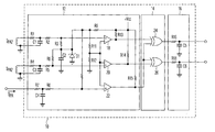
Referring to FIG. 5, there is shown on embodiment of apparatus 10 of the present invention. In this particular embodiment, apparatus 10 is configured to detect short circuits for two transformers in series wherein each transformer is associated with a corresponding lamp. However, it is to be understood that the circuit of FIG. 5 can be used with one lamp or more than two lamps. Waveform conversion circuit 12 generally comprises input signal circuitry for receiving the transformer primary voltage waveforms associated with the pair of lamps and for receiving the transformer primary current waveform. Circuit 12 includes resistors R1 and R2 and capacitor C1 which are configured as a “T” network. One end of the resistor R1 is connected to a transformer primary auxiliary winding portion TPA1 to receive voltage VPA1 which is in phase with voltage Vp. The other end of resistor R1 is connected to one end of the resistor R2 and capacitor C1. The primary auxiliary winding portion TPA1 corresponds to the transformer second winding voltage which is applied to a first lighting system or lamp. The other end of capacitor C1 is connected to a ground potential. In one embodiment, resistor R1 has a resistor of 10 kΩ and resistor R2 has a resistor of 100 kΩ. In one embodiment, capacitor C1 has a capacitance of 100 pf (picofarads). Circuit 12 further includes resistors R3, capacitor C1, and Zener diode D1. One end of the resistor R3 is connected one end of capacitor C2 and the anode of Zener diode D1. The other end of capacitor C2 is connected to a ground potential. In one embodiment, resistor R3 has a resistor of 100 kΩ. Capacitor C2 functions as a bypass capacitor and prevents A.C. signals from being applied to Zener diode D1 and in one embodiment, has a capacitance of 0.01 uf (microfarads). In on embodiment, the Zener diode D1 is about 3.3 volts. Resistor R3 and Zener diode D1 provide a D.C. offset voltage for the voltage signal VPA1.
Referring to FIG. 5, waveform conversion circuit 12 further includes resistors R4 and R5 and capacitor C3 which are configured in a “T” network. One end of resistor R4 is connected to transformer primary auxiliary winding portion TPA2 to receive voltage VPA2 which is in phase with voltage Vp. The other end of resistor R4 is connected to one end of resistor R5 and capacitor C3. Voltage VPA2 is applied to a second lighting system or lamp. The other end of capacitor C3 is connected to ground potential. In one embodiment, resistor R4 has a resistance of 10KΩ and resistor R5 has a resistance of 100KΩ. In one embodiment, capacitor C3 has a capacitance of 100 pf (picofarads). Circuit 12 further includes resistor R6. Resistor R6 is connected between resistor R5 and Zener diode D1. In one embodiment, resistor R6 has a resistance of 100KΩ. Resistor R6 and Zener diode D1 cooperate to provide a D.C. offset voltage for voltage signal VPA2.
Referring to FIG. 5, circuit 12 further includes resistors R7 and R8 and capacitor C4 which are arranged in a “T” network. In one embodiment, resistors R7 and R8 have resistances of 10KΩ and 100KΩ, respectively. In one embodiment, capacitor C4 has a capacitance of about 100 pf. The current flowing through the transformer secondary winding is inputted into one end of resistor R7. Resistor R10 and Zener diode D1 cooperate to provide a D.C. offset for current IPA which flows through transformer auxiliary winding portions TPA1 and TPA2. The current IPA is inputted into comparator 22.
Referring to FIG. 5, waveform converter circuit 12 further comprises resistors R9, R10, R11, R12, R14 and R15, and comparators 18, 20 and 22. Resistor R9 is connected between supply voltage +Vcc and the anode of Zener diode D1. In one embodiment, supply voltage +Vcc is about 5.0 volts D.C. Resistor R10 is connected between resistor R8 and the anode of Zener diode D1. Resistor R10 is also connected to the non-inverting input of comparator 22. Resistors R11 and R12 are configured in a voltage divider circuit. Resistor R11 is connected between the anode of Zener diode D1 and one end resistor R12. The other end of resistor R12 is connected to ground potential. The junction of resistors R11 and R12 is connected and provides a bias voltage to the inverting inputs of comparators 18, 20 and 22. The junction of resistors R2 and R3 is connected to the non-inverting input of comparator 18. The junction of resistors R5 and R6 is connected to the non-inverting input of comparator 20. Resistors R13, R14 and R15 function as pull-up resistors and are connected between +Vcc and the outputs of comparators 18, 20 and 22, respectively. In one embodiment, resistor R10 has a resistance of 100KΩ. In one embodiment, each resistor R9, R11, R12, R13, R14 and R15 has a resistance of 10KΩ.
Referring to FIG. 5, phase detector 14 generally comprises XOR (Exclusive OR) gates 24 and 26. One input of gate 24 is connected to the output of comparator 18. The other input of gate 24 is connected to the output of comparator 22. One input of gate 26 is connected to the output of comparator 20. The other input of gate 26 is connected to the output of comparator 22. The outputs of gates 24 and 26 are inputted into output filter circuit 16.
Referring to FIG. 5, filter circuit 16 generally comprises two R-C type filter circuits. Each R-C filter circuit receives an output from a respective XOR gate. One filter circuit comprises resistor R16 and capacitor C5. The output of XOR gate 24 is connected to resistor R16. The other filter circuit comprises resistor R18 and capacitor C6. The output of XOR gate 26 is connected to resistor R18. In one embodiment, each resistor R16 and R18 has a resistance of 100KΩ. In one embodiment, each capacitor C5 and C6 has a capacitance of 0.1 uf. The R-C filter circuits smooth out the output of the XOR gates 24 and 26 and filter out any AC ripple, ringing or transient spikes.
Operation
Referring to FIG. 5, voltage VPA1 inputted into waveform converter circuit 12. Specifically, voltage VPA1 is inputted into the input circuit comprising resistors R1 and R2 and capacitor C1. As described in the foregoing description, resistors R1 and R3 and Zener diode D1 provides a D.C. offset voltage for the voltage VPA1. Voltage VPA1 and the offset voltage are then inputted into the non-inverting input of comparator 18. Similarly, voltage VPA2 is inputted into waveform converter circuit 12. Specifically, voltage VPA2 is inputted into the input circuit comprising resistors R4 and R5 and capacitor C3.
Referring to FIG. 5, the current IPA is inputted into waveform converter circuit 12 at resistor R7. The voltages VPA1 and VPA2 and current IPA are in the form of sinusoidal waveforms. As will be explained below, comparators 18, 20 and 22 convert the sinusoidal waveforms into generally squarewave signal waveforms. Voltage VPA1, which is associated with the first lamp, is inputted into the non-inverting input of comparator 18. The output of comparator 18 is inputted into phase detector circuit 14. Specifically, the output of comparator 18 is inputted into one input of XOR gate 24. The current waveform IPA is outputted by comparator 22 and is inputted into the second input of XOR gate 24.
Referring to FIG. 6, waveforms 30 and 32 are the IPA and VPA1 waveforms, respectively, that are outputted from comparators 18 and 22, respectively, during normal conditions (i.e. no short). Waveforms 30 and 32 have an offset voltage VOS. Waveforms 30 and 32 are inputted into XOR gate 24. Waveform 34 is the output of XOR gate 24. Since the IPA and VPA1 waveforms are in phase, waveform 34 is generally at TTL logic level “LOW” indicated by voltage V1. The output of XOR gate 24 is inputted into the R-C filter circuit comprising resistor R16 and capacitor C5. Referring to FIG. 7, waveform 36 is outputted by this R-C filter circuit and is at a TTL logic level “LOW” level indicated by voltage V2 which, in one embodiment, is between about 0.1 and 0.2 volts.
Referring to FIG. 8, waveforms 40 and 44 are current signal IS and voltage VPA1 when the first lamp is shorted. Waveforms 40 and 44 are outputted from comparators 18 and 22, respectively, and are inputted into XOR gate 24. Since there is a significant phase difference between waveforms 40 and 44, XOR gate 24 outputs waveform 46 which has a TTL “HIGH” level that is indicated by voltage V3. Waveform 46 is then inputted into the R-C filter circuit comprising resistor R16 and capacitor C5. This R-C filter circuit outputs waveform 48 shown in FIG. 9. Waveform 48 is generally a D.C. voltage V4 that is at a TTL “HIGH” level of about 3.3 volts.
Referring to FIG. 5, it is to be understood that due to the symmetry of the circuit design used to realize apparatus 10, the phase difference between current IPA and voltage signal VPA2 is detected in the same manner via comparators 20 and 22, XOR gate 26 and the R-C filter comprising resistor R18 and capacitor C6. Thus, the aforementioned R-C filter circuit outputs a waveform similar to waveform 36 when the second lamp is not shorted, and a waveform similar to waveform 48 when the second lamp is shorted.
The waveforms outputted by the R-C filter comprising resistor R16 and capacitor C5 and the R-C filter comprising resistor R18 and capacitor C6 can be inputted into control circuitry (not shown) that deactivates either or both lamps if a short develops in either or both lamps.
Since the voltage swing of the output of the R-C filter circuits is relatively large, each R-C filter may be configured to have a relatively low time constant even if the output ripple of the filter is high. The relatively low time constant also allows apparatus 10 to detect short circuits in a deep-dimming configuration which typically uses relatively low, duty-cycle PWM (pulse-width-modulation).
An important advantage of apparatus of the present invention is that the per-unit cost of system 10 is relatively low because it is not necessary for apparatus 10 to detect the amplitude of the transformer's voltage and current, or circuit parameters such as leakage inductance Ls and coupling coefficients.
Although FIG. 5 shows a circuit configured for use with two lamps, it is to be understood that the present invention can be used for one lamp or more than two lamps. Furthermore, the component values (i.e. resistances and capacitances) for the resistors and capacitors described above are just examples of suitable component values. It is to be understood that other suitable component values can also be used. Furthermore, although the comparators shown in FIG. 5 are configured to operate with a single power source +Vcc, it is to be understood that the comparators can be configured to operate with two power sources.
The principals, preferred embodiments and modes of operation of the present invention have been described in the foregoing specification. The invention which is intended to be protected herein should not, however, be construed as limited to the particular forms disclosed, as these are to be regarded as illustrative rather than restrictive. Variations in changes may be made by those skilled in the art without departing from the spirit of the invention. Accordingly, the foregoing detailed description should be considered exemplary in nature and not limited to the scope and spirit of the invention as set forth in the attached claims.

Claims (15)

Thus, having described the invention, what is claimed is:
1. An apparatus for detecting a short in a load which receives power from a transformer having a primary winding and a second winding, the load being connected to the secondary winding, said apparatus comprising:
a waveform conversion circuit for converting a voltage signal and a current signal that represent a voltage signal and a current signal, respectively, of the primary winding into generally squarewave voltage and current signals, respectively, having a first DC offset voltage and a second DC offset voltage, respectively;
a phase detector circuit for outputting a control signal having a first state when the generally squarewave voltage and current signals are substantially in phase and a second state when there is a difference in phase between the generally squarewave voltage and current signals that is greater than a predetermined phase difference; and
a filter for filtering the control signal outputted by said phase detector circuit.
2. The apparatus according to claim 1, wherein said phase detector circuit includes a XOR gate having a first input for receiving the generally squarewave voltage waveform and a second input for receiving the generally squarewave current waveform.
3. The apparatus according to claim 1, wherein filter a R-C filter.
4. The apparatus of claim 1, wherein said waveform conversion circuit includes:
a resistor and a diode for providing the DC offset voltage to the received voltage signal.
5. The apparatus of claim 1, wherein said waveform conversion circuit includes:
a resistor and a diode for providing the DC offset voltage to the received current signal.
6. The apparatus of claim 1, wherein said waveform conversion circuit includes:
a capacitor and a pair of resistors configured in a T network for receiving the voltage signal.
7. The apparatus of claim 6, wherein said waveform conversion circuit further includes a comparator having a first input and a second input, said first input of said comparator in electrical communication with said T network.
8. The apparatus of claim 7, wherein a bias voltage is applied to said second input of said comparator.
9. The apparatus of claim 1, wherein said waveform conversion circuit includes:
a capacitor and a pair of resistors configured in a T network for receiving the current signal.
10. The apparatus of claim 9, wherein said waveform conversion circuit further includes a comparator having a first input and a second input, said first input of said comparator in electrical communication with said T network.
11. The apparatus of claim 10, wherein a bias voltage is applied to said second input of said comparator.
12. An apparatus for detecting a short in a lighting system that receives power from a transformer having a primary winding and a second winding, the lighting system being connected to the secondary winding, said apparatus comprising:
means for converting a voltage signal and a current signal that represent the transformer primary winding voltage and current signals respectively, into generally squarewave voltage and current signals, respectively, having a first DC offset voltage and a second DC offset voltage, respectively;
means for outputting a control signal having a first state when the generally squarewave voltage and current signals are substantially in phase and a second state when there is a difference in phase between the generally squarewave voltage and current signals that is greater than a predetermined phase difference; and
means for filtering the control signal outputted by said phase detector circuit.
13. A method for detecting a short in a load which receives power from a transformer that has a primary winding and a second winding, the load being connected to the secondary winding, said method comprising:
providing voltage and current signals that represent the voltage and current signals, respectively, of the transformer primary winding;
converting the provided voltage and current signals into generally squarewave voltage and current signals, respectively, having a first DC offset voltage and a second DC offset voltage, respectively;
generating a control signal having a first state when the generally squarewave voltage and current signals are substantially in phase and a second state when there is a difference in phase between the generally squarewave voltage and current signals that is greater than a predetermined phase difference; and
filtering the control signal.
14. The method according to claim 13, wherein the control signal having the second state indicates a short exist in the load.
15. The method according to claim 13, further comprising:
deactivating the load when the control signal has the second state.
US09/667,450 2000-09-22 2000-09-22 Apparatus and method for detecting a short circuit in a lighting system Expired - Fee Related US6496012B1 (en)

Priority Applications (5)

Application Number Priority Date Filing Date Title
US09/667,450 US6496012B1 (en) 2000-09-22 2000-09-22 Apparatus and method for detecting a short circuit in a lighting system
PCT/EP2001/010583 WO2002025791A2 (en) 2000-09-22 2001-09-12 Apparatus and method for detecting a short circuit in a lighting system
EP01980379A EP1234365A2 (en) 2000-09-22 2001-09-12 Apparatus and method for detecting a short circuit in a lighting system
CN01802826.8A CN1394373A (en) 2000-09-22 2001-09-12 Apparatus and method for detecting short circuit in lighting system
JP2002528893A JP2004509597A (en) 2000-09-22 2001-09-12 Apparatus and method for detecting short circuit in lighting device

Applications Claiming Priority (1)

Application Number Priority Date Filing Date Title
US09/667,450 US6496012B1 (en) 2000-09-22 2000-09-22 Apparatus and method for detecting a short circuit in a lighting system

Publications (1)

Publication Number Publication Date
US6496012B1 true US6496012B1 (en) 2002-12-17

Family

ID=24678277

Family Applications (1)

Application Number Title Priority Date Filing Date
US09/667,450 Expired - Fee Related US6496012B1 (en) 2000-09-22 2000-09-22 Apparatus and method for detecting a short circuit in a lighting system

Country Status (5)

Country Link
US (1) US6496012B1 (en)
EP (1) EP1234365A2 (en)
JP (1) JP2004509597A (en)
CN (1) CN1394373A (en)
WO (1) WO2002025791A2 (en)

Cited By (4)

* Cited by examiner, † Cited by third party
Publication number Priority date Publication date Assignee Title
US20080147337A1 (en) * 2005-09-12 2008-06-19 Acuity Brands, Inc. Light Management System Having Networked Intelligent Luminaire Managers with Enhanced Diagnostics Capabilities
US7817063B2 (en) 2005-10-05 2010-10-19 Abl Ip Holding Llc Method and system for remotely monitoring and controlling field devices with a street lamp elevated mesh network
CN102244380A (en) * 2010-12-22 2011-11-16 保定天威集团有限公司 Open-phase protection method and device of 35kV American box-type substation for wind power station
US8140276B2 (en) 2008-02-27 2012-03-20 Abl Ip Holding Llc System and method for streetlight monitoring diagnostics

Families Citing this family (1)

* Cited by examiner, † Cited by third party
Publication number Priority date Publication date Assignee Title
US7098745B2 (en) * 2003-06-04 2006-08-29 Intel Corporation System to control integrated circuit resonance

Citations (2)

* Cited by examiner, † Cited by third party
Publication number Priority date Publication date Assignee Title
US4228475A (en) * 1978-08-28 1980-10-14 Amf Incorporated Ground monitoring system
US5965989A (en) 1996-07-30 1999-10-12 Micro Linear Corporation Transformer primary side lamp current sense circuit

Family Cites Families (2)

* Cited by examiner, † Cited by third party
Publication number Priority date Publication date Assignee Title
US5387845A (en) * 1988-04-01 1995-02-07 Nilssen; Ole K. Neon lamp power supply
DE3888675D1 (en) * 1988-04-20 1994-04-28 Zumtobel Ag Dornbirn Ballast for a discharge lamp.

Patent Citations (2)

* Cited by examiner, † Cited by third party
Publication number Priority date Publication date Assignee Title
US4228475A (en) * 1978-08-28 1980-10-14 Amf Incorporated Ground monitoring system
US5965989A (en) 1996-07-30 1999-10-12 Micro Linear Corporation Transformer primary side lamp current sense circuit

Cited By (11)

* Cited by examiner, † Cited by third party
Publication number Priority date Publication date Assignee Title
US20080147337A1 (en) * 2005-09-12 2008-06-19 Acuity Brands, Inc. Light Management System Having Networked Intelligent Luminaire Managers with Enhanced Diagnostics Capabilities
US7761260B2 (en) 2005-09-12 2010-07-20 Abl Ip Holding Llc Light management system having networked intelligent luminaire managers with enhanced diagnostics capabilities
US7911359B2 (en) 2005-09-12 2011-03-22 Abl Ip Holding Llc Light management system having networked intelligent luminaire managers that support third-party applications
US8010319B2 (en) 2005-09-12 2011-08-30 Abl Ip Holding Llc Light management system having networked intelligent luminaire managers
US8260575B2 (en) 2005-09-12 2012-09-04 Abl Ip Holding Llc Light management system having networked intelligent luminaire managers
US7817063B2 (en) 2005-10-05 2010-10-19 Abl Ip Holding Llc Method and system for remotely monitoring and controlling field devices with a street lamp elevated mesh network
US8140276B2 (en) 2008-02-27 2012-03-20 Abl Ip Holding Llc System and method for streetlight monitoring diagnostics
US8442785B2 (en) 2008-02-27 2013-05-14 Abl Ip Holding Llc System and method for streetlight monitoring diagnostics
US8594976B2 (en) 2008-02-27 2013-11-26 Abl Ip Holding Llc System and method for streetlight monitoring diagnostics
CN102244380A (en) * 2010-12-22 2011-11-16 保定天威集团有限公司 Open-phase protection method and device of 35kV American box-type substation for wind power station
CN102244380B (en) * 2010-12-22 2013-09-11 保定天威集团有限公司 Open-phase protection method and device of 35kV American box-type substation for wind power station

Also Published As

Publication number Publication date
WO2002025791A3 (en) 2002-06-13
JP2004509597A (en) 2004-03-25
CN1394373A (en) 2003-01-29
WO2002025791A2 (en) 2002-03-28
EP1234365A2 (en) 2002-08-28

Similar Documents

Publication Publication Date Title
US4943886A (en) Circuitry for limiting current between power inverter output terminals and ground
US5075599A (en) Circuit arrangement
KR900004349B1 (en) Dc component corrector for inverter output voltage
US7595644B2 (en) Power-over-ethernet isolation loss detector
US10536071B2 (en) Detecting ground faults on non-isolated DC systems
EP0482705A2 (en) Circuit arrangement
US20220312565A1 (en) An isolated converter and led driver using the isolated converter
WO2008104919A1 (en) Load current detection in electrical power converters
US6084785A (en) Electric power converter
US6496012B1 (en) Apparatus and method for detecting a short circuit in a lighting system
US5548207A (en) Missing phase detector
US5668708A (en) DC power supply with reduced ripple
FI85062B (en) FREQUENCY REQUIREMENTS FOR THE MAINTENANCE OF STREETS WITH FREQUENCY FORM.
JP2000166205A (en) Interphase short circuit detector
TWI599177B (en) Zero crossing detector using current mode approach
JP2002305882A (en) Power converter
JPH10322883A (en) Power converter
CN219162251U (en) Three-phase power supply detection circuit and electric welding machine
US5459417A (en) Apparatus for detecting DC content of an AC waveform
US6005381A (en) Electrical signal phase detector
CN108375797A (en) A kind of system that foreign bodies detection is carried out by sample rate current phase difference
KR101642486B1 (en) Inverter device and driving method thereof
KR100396330B1 (en) Device for alerting receiving an electric shock of heavy equipment
KR100643937B1 (en) Limited current apparatus for parallel inverter
NL8303319A (en) ACTIVE DOUBLE-SIDED RADIATOR.

Legal Events

Date Code Title Description
AS Assignment

Owner name: PHILIPS ELECTRONICS NORTH AMERICA CORPORATION, NEW

Free format text: ASSIGNMENT OF ASSIGNORS INTEREST;ASSIGNORS:WENG, DA FENG;CHANG, CHIN;REEL/FRAME:011112/0633

Effective date: 20000913

AS Assignment

Owner name: KONINKLIJKE PHILIPS ELECTRONICS N.V., NETHERLANDS

Free format text: ASSIGNMENT OF ASSIGNORS INTEREST;ASSIGNOR:PHILIPS ELECTRONICS NORTH AMERICA CORPORATION;REEL/FRAME:013402/0746

Effective date: 20021011

REMI Maintenance fee reminder mailed
LAPS Lapse for failure to pay maintenance fees
STCH Information on status: patent discontinuation

Free format text: PATENT EXPIRED DUE TO NONPAYMENT OF MAINTENANCE FEES UNDER 37 CFR 1.362

FP Lapsed due to failure to pay maintenance fee

Effective date: 20061217