US6496160B1 - Stroke to raster converter system - Google Patents
Stroke to raster converter system Download PDFInfo
- Publication number
- US6496160B1 US6496160B1 US09/301,947 US30194799A US6496160B1 US 6496160 B1 US6496160 B1 US 6496160B1 US 30194799 A US30194799 A US 30194799A US 6496160 B1 US6496160 B1 US 6496160B1
- Authority
- US
- United States
- Prior art keywords
- stroke
- major
- analog
- character
- level
- Prior art date
- Legal status (The legal status is an assumption and is not a legal conclusion. Google has not performed a legal analysis and makes no representation as to the accuracy of the status listed.)
- Expired - Fee Related
Links
Images

Classifications
-
- G—PHYSICS
- G09—EDUCATION; CRYPTOGRAPHY; DISPLAY; ADVERTISING; SEALS
- G09G—ARRANGEMENTS OR CIRCUITS FOR CONTROL OF INDICATING DEVICES USING STATIC MEANS TO PRESENT VARIABLE INFORMATION
- G09G1/00—Control arrangements or circuits, of interest only in connection with cathode-ray tube indicators; General aspects or details, e.g. selection emphasis on particular characters, dashed line or dotted line generation; Preprocessing of data
- G09G1/06—Control arrangements or circuits, of interest only in connection with cathode-ray tube indicators; General aspects or details, e.g. selection emphasis on particular characters, dashed line or dotted line generation; Preprocessing of data using single beam tubes, e.g. three-dimensional or perspective representation, rotation or translation of display pattern, hidden lines, shadows
- G09G1/07—Control arrangements or circuits, of interest only in connection with cathode-ray tube indicators; General aspects or details, e.g. selection emphasis on particular characters, dashed line or dotted line generation; Preprocessing of data using single beam tubes, e.g. three-dimensional or perspective representation, rotation or translation of display pattern, hidden lines, shadows with combined raster scan and calligraphic display
-
- G—PHYSICS
- G09—EDUCATION; CRYPTOGRAPHY; DISPLAY; ADVERTISING; SEALS
- G09G—ARRANGEMENTS OR CIRCUITS FOR CONTROL OF INDICATING DEVICES USING STATIC MEANS TO PRESENT VARIABLE INFORMATION
- G09G5/00—Control arrangements or circuits for visual indicators common to cathode-ray tube indicators and other visual indicators
- G09G5/36—Control arrangements or circuits for visual indicators common to cathode-ray tube indicators and other visual indicators characterised by the display of a graphic pattern, e.g. using an all-points-addressable [APA] memory
- G09G5/39—Control of the bit-mapped memory
- G09G5/393—Arrangements for updating the contents of the bit-mapped memory
-
- G—PHYSICS
- G09—EDUCATION; CRYPTOGRAPHY; DISPLAY; ADVERTISING; SEALS
- G09G—ARRANGEMENTS OR CIRCUITS FOR CONTROL OF INDICATING DEVICES USING STATIC MEANS TO PRESENT VARIABLE INFORMATION
- G09G5/00—Control arrangements or circuits for visual indicators common to cathode-ray tube indicators and other visual indicators
- G09G5/36—Control arrangements or circuits for visual indicators common to cathode-ray tube indicators and other visual indicators characterised by the display of a graphic pattern, e.g. using an all-points-addressable [APA] memory
- G09G5/39—Control of the bit-mapped memory
- G09G5/395—Arrangements specially adapted for transferring the contents of the bit-mapped memory to the screen
-
- G—PHYSICS
- G09—EDUCATION; CRYPTOGRAPHY; DISPLAY; ADVERTISING; SEALS
- G09G—ARRANGEMENTS OR CIRCUITS FOR CONTROL OF INDICATING DEVICES USING STATIC MEANS TO PRESENT VARIABLE INFORMATION
- G09G5/00—Control arrangements or circuits for visual indicators common to cathode-ray tube indicators and other visual indicators
- G09G5/36—Control arrangements or circuits for visual indicators common to cathode-ray tube indicators and other visual indicators characterised by the display of a graphic pattern, e.g. using an all-points-addressable [APA] memory
- G09G5/39—Control of the bit-mapped memory
- G09G5/399—Control of the bit-mapped memory using two or more bit-mapped memories, the operations of which are switched in time, e.g. ping-pong buffers
Definitions
- This invention relates to apparatus and method for converting analog stroke display signals to raster display information for developing a raster-scan image display.
- Computer graphics involves the development of images for display on some type of display device.
- the display devices developed and used initially in computer graphics were known as a vector, stroke or line drawing displays.
- vector and “stroke” are synonymous with “line”.
- To develop characters for display the character outlines were composed of sequences of strokes, produced by moving an electron beam of a cathode ray tube (CRT) to draw the character on the phosphor coating of the CRT screen.
- CTR cathode ray tube
- the electron beam is deflected, to draw the character, by beam-deflection circuits in response to analog voltages developed by a vector or stroke generator.
- the stroke generator of a stroke display device typically develops an analog X major deflection signal and an analog Y major deflection signal for moving the electron beam from one general location to another. Some stroke generators also developed an additional analog x character deflection signal and an additional analog y character deflection signal for guiding the electron beam within the general location to which the beam has been moved, to draw or trace a line, character, symbol, etc.
- the final signal typically developed by a stroke generator is a three voltage level video signal, having a 0 volt level to indicate that the electron beam is off (a condition where the beam is to be moved from one location to another without producing a trace), a 1 volt level defining a certain brightness of the trace when moving the beam from one general location to another to produce a trace, but not to draw a character, and a 2 volt level for increasing the brightness of the trace when drawing a character after the beam has been moved to a desired character location.
- the brightness is increased when drawing a character since the movement of the beam is much faster than when simply moving the beam from one location to another; the voltage level must be boosted just to maintain the brightness of the drawn character to about the same as the brightness of the trace.
- Raster displays store so-called display primitives (such as lines, characters, and solidly shaded or patterned areas) in a refresh buffer, in the form of component pixels.
- the image on a raster display device is formed from a set of horizontal raster lines, each line containing a row of individual pixels.
- the “raster” is stored in a frame buffer as a matrix of pixels representing the entire screen (frame) area.
- the image is scanned out sequentially by a video controller, one raster line at a time, from top to bottom and then back to the top, in the same manner as a television picture or image is created.
- Each pixel includes information to determine the electron beams intensity when being moved through that pixel location on the screen. All this is well known technology and a full description and discussion is given in Foley, James D. et al., Computer Graphics Principles and Practice , Addison-Wesley Publishing Company, 1996.
- Raster displays have a number of advantages over stroke displays including the need for less expensive image generating logic. Also, raster displays can fill areas with a uniform color or a repeated pattern in two or more colors, and can store images in a way that allows manipulation at a fine level, including the copying or moving of selected portions of an image.
- a raster display compared to a stroke display, results from the discrete nature of the pixel representation. Primitives are specified in terms of their end points (vertices) and must be scan-converted into their component pixels in the frame buffer. Because each primitive must be scan-converted, real-time processing is computationally more complicated for raster displays than for stroke displays. Nevertheless, most computer graphics systems today utilize raster displays.
- stroke display systems Because large numbers of stroke display systems had been installed in the past and many are still in use today (for example, stroke display systems are common in commercial and military aircraft), it has been found desirable, when upgrading an existing stroke display system, to save as much of the existing circuitry as possible, especially the stroke generator circuitry.
- stroke to raster converters have been developed to enable use of the stroke generator, but to convert the stroke generation signals to raster producing signals for use on a raster display device. In effect, a raster display replaces the stroke display to develop the desired images.
- the prior art approach to converting from stroke to raster displays involved sampling the analog stroke signals to obtain data indicating the brightness of the stroke trace, and then adding the samples for corresponding similar pixel locations to obtain a composite pixel representation of the stroke trace.
- a problem with this approach is that for crossing or intersecting traces, the trace would be sampled twice where the trace is crossed or intersected, and the pixel representation of such crossing or intersection would be an excessively bright spot.
- the image would be quite disconcerting when viewed because of the number of excessively bright spots.
- the above and other objects are realized in an illustrative embodiment of apparatus for converting stroke display signals (representing electron beam generated stroke traces) into raster display information for developing a raster video image display.
- the apparatus includes a sampling circuit for sampling the analog stroke display signals to produce pixel data representing pixel locations covered or touched by the stroke traces, a frame buffer for temporarily storing the pixel data samples for subsequent supply to a raster display device.
- the sampling circuit is adapted to sample at a rate sufficient to allow development of digital representations of pixels subdivided into arrays of sub-pixels with indications of which sub-pixel locations were covered or drawn by the stroke trace.
- a filter is provided between the frame buffer and the display device for calculating brightness of pixels based upon the amount of A coverage of the pixel by the stroke trace.
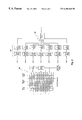
- FIG. 1 is a block diagram representation of a stroke to raster converter made in accordance with the principles of the present invention
- FIG. 2 is a schematic representation of one illustrative embodiment and implementation of the converter of FIG. 1;
- FIG. 3 is a schematic representation of one embodiment of a detailed implementation of the filter of FIG. 2 .
- FIG. 1 there is shown one illustrative embodiment of a stroke to raster converter 4 for receiving analog stroke signals from a stroke generator 8 and for converting those signals to pixel data for producing a raster image for display on a raster display device 12 .
- the stroke-generator 8 develops five analog signals, as discussed previously, including an X major deflection signal, a Y major deflection signal, (defining respectively the X axis and Y axis end point coordinates of a stroke trace), an x character deflection signal, a y character deflection signal (defining respectively the x axis and y axis coordinates of a character stroke trace as a character is being drawn), and a three-level video signal in which a voltage level of 0 indicates that the electron beam is to be moved but the beam is off, a voltage level of 1 indicates that a stroke trace or line is to be drawn by the electron beam at a first brightness level, and a voltage level of 2 indicates that a character is to be drawn by the electron beam at the general location to which the electron beam has been moved, with the character trace to be at a second higher brightness level.
- a 0 voltage level means move the electron beam but don't produce a trace
- a 1 voltage level means draw strokes and conic
- the X and Y major deflection signals and x and y character deflection signals are sampled by a sub-pixel sampler 16 at rates and resolutions that correspond to four samples per pixel in each of the x and y axes. For example, for the X and Y major deflection signals, a sampling at 22.5 Mhz to twelve bits of resolution could be utilized, and for the x and y character deflection signals, the sampling could be carried out at 45 Mhz to eight bits of resolution.
- the above exemplary sampling results in a four-by-four array of sixteen sub-pixels or bits for each pixel location (to be displayed on the raster display device 12 where a sub-pixel shows a “1” if the sub-pixel was covered or touched by the stroke trace being sampled and a “0” if the sub-pixel was not covered or touched by the stroke trace.
- the pixels composed of sixteen sub-pixels, are supplied to a frame buffer memory 20 for temporary storage and for ultimate supply to a filter 24 and then to the raster display device 12 to enable producing the raster images.
- the sub-pixels in the frame buffer memory 20 are set at “1” if those sub-pixels are covered by only one stroke trace or many stroke traces (i.e., if a sub-pixel is drawn one or many times), and set at “0” if the sub-pixels are not covered (i.e., the sub-pixel locations are not drawn).
- the result is that no pixel locations on the raster display will have a disconcerting increase in brightness simply because that pixel represents an intersection or crossing of stroke traces, as with prior art stroke to raster converter systems.
- the filter 24 calculates the intensity of a given pixel from the sub-pixel samples of the given pixel and from adjacent pixels. This results in smoother appearing lines and edges of objects to be displayed on the raster display unit 12 .
- FIG. 2 illustrates representative components of the sub-pixel sampler 16 , frame buffer memory 20 , and filter 24 and will now be discussed.
- a stroke analog process/digital sampler 34 samples the X major and Y major deflection signals and the x and y character deflection signals as previously described, and effectively operates as an analog-to-digital converter to produce digitized samples.
- the digitized samples are supplied to a major and character combiner 38 , along with the previously described three-level video signal (labeled “stroke video” in FIG. 2 ).
- the combiner 38 adds the digitized samples of the X major and x character deflection signals, and adds the digitized samples of the Y major and y character deflection signals, and supplies the sums respectively on an X output line 40 and a Y output line 42 to an input first in, first out (FIFO) memory 46 .
- the stroke video signal is at level 1, indicating that no character is being drawn but that the electron beam is being moved from one location to another while drawing a stroke trace, the digitized samples of the X major and Y major deflection signals are passed respectively via lines 40 and 42 to the input FIFO memory 46 .
- the stroke video signal is at level 0 indicating that no character or stroke trace is being drawn, i.e., the electron beam is off, then no digitized samples or signals are supplied to the input FIFO memory 46 .
- the data supplied to and stored in the input FIFO memory 46 might consist of a twelve bit Y deflection value and a thirteen bit X deflection value (the X deflection value contains more bits to accommodate the larger number of pixels arranged horizontally across a typical display screen than are arranged vertically) representing a sub-pixel location on the screen of the raster display device 12 .
- the input FIFO memory 46 is provided as buffer since the input processing to the FIFO memory is being carried out faster than the output processing (see the frequency graph 50 shown below in the schematic in FIG. 2 to indicate exemplary processing speeds for the different portions of the schematic).
- adjacent sub-pixel samples are combined into pixel samples as follows.
- the low order two bits of the X and Y deflection values define the sub-pixel location within the pixel (made up of sixteen sub-pixels arranged in four rows of four sub-pixels).
- the rest of the bits define the pixel location.
- the sub-pixel sampler 16 (FIG. 1) includes a sub-pixel cache 54 (FIG. 2) to which the sub-pixels making up a pixel are supplied from the input FIFO memory 46 and temporarily stored.
- the cache 54 will only store the sub pixels of a single pixel. When the sub-pixels from another pixel arrive the contents of the cache are written into the frame buffer 20 . The sub-pixel cache 54 is then cleared and the bit associated with the next sampled sub-pixel in the new pixel location is written into the cache.
- the frame buffer memory 20 includes a conventional frame buffer memory control unit 58 and two “swappable” frame buffers 62 . While one of the frame buffers 62 is supplying pixel data to the filter 24 (for ultimate delivery to the raster display unit 12 to develop a raster image), the other frame buffer is being loaded with the next frame of pixel data. When that loading is complete, and the first-mentioned frame buffer is completely “unloaded”, then loading of the first-mentioned frame buffer begins and unloading of the other frame buffer also begins. This is carried out under control of the frame buffer memory control unit 58 in a conventional fashion.
- the frame buffer 62 might advantageously be comprised of video random access memories (VRAMs).
- the output portion of the stroke to raster converter of FIG. 2 is designed to create video images for display on a liquid crystal display (LCD) or CRT display in real-time from the sub-pixel data stored in the frame buffers 62 .
- LCD liquid crystal display
- an even/odd pixel pair would be supplied to the panel, for example, approximately every eighteen nanoseconds (5.5 MHz)).
- the rate at which pixels would be produced is reduced to one pair per 22.5 nanoseconds (45 MHz.) by utilizing the entire horizontal line time to produce the active pixels and store them in a FIFO memory 78 .
- the pixels are supplied to the LCD panel one line later at the required 55 MHz rate under control of an output video format controller 66 . Note again that the speed at which the various components of the stroke to raster converter of FIG. 2 operate is shown in the frequency graph 50 located below the schematic in FIG. 2 .
- the process of producing the video pixel pairs and storing them in the FIFO memory 78 is synchronized to the output video timing on a line by line basis.
- a request is generated by the output controller 66 and supplied to the frame buffer memory control 58 to read a scan line of data into one of the two frame buffers 62 .
- the even/odd pixel pairs are presented to line delay FIFOs 68 and 70 consisting, for example, of four FIFOs. Two of the FIFOs handle the odd pixels and the other two handle the even pixels, all in parallel.
- the output of the first pair of FIFOs is supplied to the input of the second pair of FIFOs, with the FIFO read and write “enables” being arranged so that each FIFO represents one line.
- the data thus available from the frame buffer 62 , line delay FIFO 68 and line delay FIFO 70 represents a block of pixels three,lines high and two pixels wide, and this data is supplied simultaneously to separate even/odd pixel processors 74 .
- the even/odd pixel processor 74 calculates the intensity of the pixels for ultimate display on the raster display unit 12 (FIG. 1 ). The pixels with intensity designations are then supplied to an output FIFO memory 78 , for transfer to the raster display unit 12 in accordance with the video timing required by the display unit.
- the intensity of a given pixel is calculated from the sub-pixel samples of a nine-pixel area composed of the given pixel and the eight adjacent pixels.
- the information needed to calculate the intensity of a pixel is available by looking at the data from the current six-pixel area (discussed above) and the Previously processed and saved six-pixel area.
- the current and previous six-pixel areas represent a twelve-pixel area of the raster display unit screen, and the even pixel intensities are calculated from a nine-pixel area which does not include the last column of the twelve-pixel area, while the odd pixel intensities are calculated from a nine-pixel area that does not include the first column of pixels of the twelve-pixel area.
- This processing approach is convenient for dealing with the even/odd pixel pair supplied to the even/odd pixel processor 74 .
- FIG. 3 shows further details of the filter 24 and even/odd pixel processor 74 (FIG. 2) including a representative nine-pixel area 80 from which the intensity of the center pixel would be calculated.
- each pixel is composed of sixteen sub-pixels or bits, and the sub-pixels are grouped into seven zones based on the distance of each sub-pixel from the center of the pixel of interest.
- the corners of the nine-pixel grouping are not assigned to a zone and are not included in the calculation of the brightness of the center pixel so that the area used to calculate brightness is roughly circular.
- the contribution to brightness or intensity by the sub-pixels in each zone is a function of (1) how many of such sub-pixels were drawn or covered by a stroke trace and (2) a zone weight.
- the zone weights are assigned so that those close to the center of the area have the most weight while those at the edge don't contribute as much.
- the intensity for the center pixel of a nine-pixel area is calculated by counting or adding the number of sub-pixels in each zone which are drawn or covered by a stroke trace and then multiplying that sum by the weight assigned to that zone using a table lookup operation.
- a summing tree logic configuration 84 (FIG. 3) is employed to do this.
- the products for each zone calculation are then supplied to an adder 88 , which sums the products to produce a resulting intensity value for the pixel of interest. This output is then supplied to the raster display 12 (FIG. 1) for generation of the image.
Abstract
Description
Claims (10)
Priority Applications (1)
| Application Number | Priority Date | Filing Date | Title |
|---|---|---|---|
| US09/301,947 US6496160B1 (en) | 1999-04-29 | 1999-04-29 | Stroke to raster converter system |
Applications Claiming Priority (1)
| Application Number | Priority Date | Filing Date | Title |
|---|---|---|---|
| US09/301,947 US6496160B1 (en) | 1999-04-29 | 1999-04-29 | Stroke to raster converter system |
Publications (1)
| Publication Number | Publication Date |
|---|---|
| US6496160B1 true US6496160B1 (en) | 2002-12-17 |
Family
ID=23165589
Family Applications (1)
| Application Number | Title | Priority Date | Filing Date |
|---|---|---|---|
| US09/301,947 Expired - Fee Related US6496160B1 (en) | 1999-04-29 | 1999-04-29 | Stroke to raster converter system |
Country Status (1)
| Country | Link |
|---|---|
| US (1) | US6496160B1 (en) |
Cited By (17)
| Publication number | Priority date | Publication date | Assignee | Title |
|---|---|---|---|---|
| US20030025831A1 (en) * | 2001-04-03 | 2003-02-06 | Seals James M. | Video converter board |
| US20040001067A1 (en) * | 2002-06-28 | 2004-01-01 | Nvidia Corporation | System and method for filtering graphics data on scanout to a monitor |
| US20040159636A1 (en) * | 1999-09-09 | 2004-08-19 | Torbjorn Sandstrom | Data path for high performance pattern generator |
| US20040217964A1 (en) * | 2003-04-30 | 2004-11-04 | International Business Machines Corporation | Method and system for providing useable images on a high resolution display when a 2D graphics window is utilized with a 3D graphics window |
| US20050093978A1 (en) * | 1998-05-27 | 2005-05-05 | William Biagiotti | Video generation and capture techniques |
| US20060017743A1 (en) * | 2004-07-23 | 2006-01-26 | Chan Victor G | Display intensity filter |
| US20060050079A1 (en) * | 2002-10-31 | 2006-03-09 | Moshe Ben-Chorin | System and method of selective adjustment of a color display |
| US20060132491A1 (en) * | 2004-12-20 | 2006-06-22 | Nvidia Corporation | Real-time display post-processing using programmable hardware |
| US20070242136A1 (en) * | 1998-05-27 | 2007-10-18 | William Biagiotti | Video generation and capture techniques |
| US20100271542A1 (en) * | 2009-04-27 | 2010-10-28 | Brian Rodgers | Stroke-to-raster video conversion method having error correction capabilities |
| US7891818B2 (en) | 2006-12-12 | 2011-02-22 | Evans & Sutherland Computer Corporation | System and method for aligning RGB light in a single modulator projector |
| US8077378B1 (en) | 2008-11-12 | 2011-12-13 | Evans & Sutherland Computer Corporation | Calibration system and method for light modulation device |
| US8358317B2 (en) | 2008-05-23 | 2013-01-22 | Evans & Sutherland Computer Corporation | System and method for displaying a planar image on a curved surface |
| US8497908B1 (en) | 2011-12-13 | 2013-07-30 | Advanced Testing Technologies, Inc. | Unified video test apparatus |
| US8702248B1 (en) | 2008-06-11 | 2014-04-22 | Evans & Sutherland Computer Corporation | Projection method for reducing interpixel gaps on a viewing surface |
| US9641826B1 (en) | 2011-10-06 | 2017-05-02 | Evans & Sutherland Computer Corporation | System and method for displaying distant 3-D stereo on a dome surface |
| EP4033481A1 (en) * | 2021-01-25 | 2022-07-27 | Thales | System and method for processing data for displaying traces in jumper mode provided by a symbol generator unit |
Citations (4)
| Publication number | Priority date | Publication date | Assignee | Title |
|---|---|---|---|---|
| US4633243A (en) * | 1983-06-30 | 1986-12-30 | International Business Machines Corporation | Method of storing characters in a display system |
| US5489920A (en) * | 1989-10-16 | 1996-02-06 | Apple Computer, Inc. | Method for determining the optimum angle for displaying a line on raster output devices |
| US5557297A (en) * | 1994-06-08 | 1996-09-17 | Smiths Industries | System for displaying calligraphic video on raster displays |
| US5969699A (en) * | 1996-10-08 | 1999-10-19 | Kaiser Aerospace & Electronics Company | Stroke-to-stroke |
-
1999
- 1999-04-29 US US09/301,947 patent/US6496160B1/en not_active Expired - Fee Related
Patent Citations (4)
| Publication number | Priority date | Publication date | Assignee | Title |
|---|---|---|---|---|
| US4633243A (en) * | 1983-06-30 | 1986-12-30 | International Business Machines Corporation | Method of storing characters in a display system |
| US5489920A (en) * | 1989-10-16 | 1996-02-06 | Apple Computer, Inc. | Method for determining the optimum angle for displaying a line on raster output devices |
| US5557297A (en) * | 1994-06-08 | 1996-09-17 | Smiths Industries | System for displaying calligraphic video on raster displays |
| US5969699A (en) * | 1996-10-08 | 1999-10-19 | Kaiser Aerospace & Electronics Company | Stroke-to-stroke |
Cited By (27)
| Publication number | Priority date | Publication date | Assignee | Title |
|---|---|---|---|---|
| US7289159B1 (en) * | 1998-05-27 | 2007-10-30 | Advanced Testing Technologies, Inc. | Video generation and capture techniques |
| US20070242136A1 (en) * | 1998-05-27 | 2007-10-18 | William Biagiotti | Video generation and capture techniques |
| US7495674B2 (en) | 1998-05-27 | 2009-02-24 | Advanced Testing Technologies, Inc. | Video generation and capture techniques |
| US20050093978A1 (en) * | 1998-05-27 | 2005-05-05 | William Biagiotti | Video generation and capture techniques |
| US7590966B2 (en) * | 1999-09-09 | 2009-09-15 | Micronic Laser Systems Ab | Data path for high performance pattern generator |
| US20040159636A1 (en) * | 1999-09-09 | 2004-08-19 | Torbjorn Sandstrom | Data path for high performance pattern generator |
| US20030025831A1 (en) * | 2001-04-03 | 2003-02-06 | Seals James M. | Video converter board |
| US6844875B2 (en) * | 2001-04-03 | 2005-01-18 | The United States Of America As Represented By The Secretary Of The Navy | Video converter board |
| US6870542B2 (en) * | 2002-06-28 | 2005-03-22 | Nvidia Corporation | System and method for filtering graphics data on scanout to a monitor |
| US20040001067A1 (en) * | 2002-06-28 | 2004-01-01 | Nvidia Corporation | System and method for filtering graphics data on scanout to a monitor |
| US20060050079A1 (en) * | 2002-10-31 | 2006-03-09 | Moshe Ben-Chorin | System and method of selective adjustment of a color display |
| US7015920B2 (en) | 2003-04-30 | 2006-03-21 | International Business Machines Corporation | Method and system for providing useable images on a high resolution display when a 2D graphics window is utilized with a 3D graphics window |
| US20040217964A1 (en) * | 2003-04-30 | 2004-11-04 | International Business Machines Corporation | Method and system for providing useable images on a high resolution display when a 2D graphics window is utilized with a 3D graphics window |
| US20060017743A1 (en) * | 2004-07-23 | 2006-01-26 | Chan Victor G | Display intensity filter |
| US20060132491A1 (en) * | 2004-12-20 | 2006-06-22 | Nvidia Corporation | Real-time display post-processing using programmable hardware |
| US7586492B2 (en) | 2004-12-20 | 2009-09-08 | Nvidia Corporation | Real-time display post-processing using programmable hardware |
| US7891818B2 (en) | 2006-12-12 | 2011-02-22 | Evans & Sutherland Computer Corporation | System and method for aligning RGB light in a single modulator projector |
| US8358317B2 (en) | 2008-05-23 | 2013-01-22 | Evans & Sutherland Computer Corporation | System and method for displaying a planar image on a curved surface |
| US8702248B1 (en) | 2008-06-11 | 2014-04-22 | Evans & Sutherland Computer Corporation | Projection method for reducing interpixel gaps on a viewing surface |
| US8077378B1 (en) | 2008-11-12 | 2011-12-13 | Evans & Sutherland Computer Corporation | Calibration system and method for light modulation device |
| US8294729B2 (en) | 2009-04-27 | 2012-10-23 | Scram Technologies, Inc. | Stroke-to-raster video conversion method having error correction capabilities |
| US20100271542A1 (en) * | 2009-04-27 | 2010-10-28 | Brian Rodgers | Stroke-to-raster video conversion method having error correction capabilities |
| US9641826B1 (en) | 2011-10-06 | 2017-05-02 | Evans & Sutherland Computer Corporation | System and method for displaying distant 3-D stereo on a dome surface |
| US10110876B1 (en) | 2011-10-06 | 2018-10-23 | Evans & Sutherland Computer Corporation | System and method for displaying images in 3-D stereo |
| US8497908B1 (en) | 2011-12-13 | 2013-07-30 | Advanced Testing Technologies, Inc. | Unified video test apparatus |
| EP4033481A1 (en) * | 2021-01-25 | 2022-07-27 | Thales | System and method for processing data for displaying traces in jumper mode provided by a symbol generator unit |
| FR3119262A1 (en) * | 2021-01-25 | 2022-07-29 | Thales | A system and method for processing jumper mode plot display data provided by a symbol generator box. |
Similar Documents
| Publication | Publication Date | Title |
|---|---|---|
| US6496160B1 (en) | Stroke to raster converter system | |
| US4967392A (en) | Drawing processor for computer graphic system using a plurality of parallel processors which each handle a group of display screen scanlines | |
| KR910009101B1 (en) | Image synthesizing apparatus | |
| US4225861A (en) | Method and means for texture display in raster scanned color graphic | |
| US5990912A (en) | Virtual address access to tiled surfaces | |
| US4725831A (en) | High-speed video graphics system and method for generating solid polygons on a raster display | |
| US4532605A (en) | True zoom of a displayed image | |
| US4570233A (en) | Modular digital image generator | |
| US5748178A (en) | Digital video system and methods for efficient rendering of superimposed vector graphics | |
| US5761401A (en) | Parallel image generation from cumulative merging of partial geometric images | |
| EP0447225B1 (en) | Methods and apparatus for maximizing column address coherency for serial and random port accesses in a frame buffer graphics system | |
| EP0660295A2 (en) | Method and apparatus for NTSC display of full motion animation | |
| JPH0695273B2 (en) | Display control device | |
| EP0201210B1 (en) | Video display system | |
| EP0098868A1 (en) | Apparatus for controling a color display. | |
| JPH0126072B2 (en) | ||
| US4631532A (en) | Raster display generator for hybrid display system | |
| US5448264A (en) | Method and apparatus for separate window clipping and display mode planes in a graphics frame buffer | |
| US5321805A (en) | Raster graphics engine for producing graphics on a display | |
| US5287442A (en) | Serpentine rendering of antialiased vectors in a computer graphics system | |
| US7616200B1 (en) | System for reducing aliasing on a display device | |
| US6567092B1 (en) | Method for interfacing to ultra-high resolution output devices | |
| US6271850B1 (en) | Image generation apparatus, image generation method, image generation program recording medium, image composition apparatus, image composition method, and image composition program recording medium | |
| EP1092217B1 (en) | Method of and system for detecting and rendering of graphic elements | |
| US4614941A (en) | Raster-scan/calligraphic combined display system for high speed processing of flight simulation data |
Legal Events
| Date | Code | Title | Description |
|---|---|---|---|
| AS | Assignment |
Owner name: EVANS & SUTHERLAND COMPUTER CORPORATION, UTAH Free format text: ASSIGNMENT OF ASSIGNORS INTEREST;ASSIGNORS:TANNER, ALLEN H.;SIMMONS, CALVIN L.;REEL/FRAME:009939/0357 Effective date: 19990426 |
|
| AS | Assignment |
Owner name: FOOTHILL CAPITAL CORPORATION, CALIFORNIA Free format text: SECURITY INTEREST;ASSIGNOR:EVAN & SUTHERLAND COMPUTER CORPORATION;REEL/FRAME:011369/0944 Effective date: 20001214 |
|
| AS | Assignment |
Owner name: EVANS & SUTHERLAND COMPUTER CORPORATION, UTAH Free format text: RELEASE OF SECURITY INTERESTS;ASSIGNOR:FOOTHILL CAPITAL CORPORATION;REEL/FRAME:017015/0428 Effective date: 20050517 |
|
| FEPP | Fee payment procedure |
Free format text: PAT HOLDER NO LONGER CLAIMS SMALL ENTITY STATUS, ENTITY STATUS SET TO UNDISCOUNTED (ORIGINAL EVENT CODE: STOL); ENTITY STATUS OF PATENT OWNER: SMALL ENTITY Free format text: PAT HOLDER CLAIMS SMALL ENTITY STATUS, ENTITY STATUS SET TO SMALL (ORIGINAL EVENT CODE: LTOS); ENTITY STATUS OF PATENT OWNER: SMALL ENTITY |
|
| REFU | Refund |
Free format text: REFUND - PAYMENT OF MAINTENANCE FEE, 4TH YEAR, LARGE ENTITY (ORIGINAL EVENT CODE: R1551); ENTITY STATUS OF PATENT OWNER: SMALL ENTITY |
|
| FPAY | Fee payment |
Year of fee payment: 4 |
|
| REMI | Maintenance fee reminder mailed | ||
| LAPS | Lapse for failure to pay maintenance fees | ||
| STCH | Information on status: patent discontinuation |
Free format text: PATENT EXPIRED DUE TO NONPAYMENT OF MAINTENANCE FEES UNDER 37 CFR 1.362 |
|
| FP | Lapsed due to failure to pay maintenance fee |
Effective date: 20101217 |