US6497141B1 - Parametric resonance in microelectromechanical structures - Google Patents
Parametric resonance in microelectromechanical structures Download PDFInfo
- Publication number
- US6497141B1 US6497141B1 US09/586,976 US58697600A US6497141B1 US 6497141 B1 US6497141 B1 US 6497141B1 US 58697600 A US58697600 A US 58697600A US 6497141 B1 US6497141 B1 US 6497141B1
- Authority
- US
- United States
- Prior art keywords
- actuator
- frequency
- substrate
- motion
- amplitude
- Prior art date
- Legal status (The legal status is an assumption and is not a legal conclusion. Google has not performed a legal analysis and makes no representation as to the accuracy of the status listed.)
- Expired - Fee Related, expires
Links
- 238000000034 method Methods 0.000 claims abstract description 33
- 230000007704 transition Effects 0.000 claims abstract description 23
- 230000009467 reduction Effects 0.000 claims abstract description 13
- 230000003416 augmentation Effects 0.000 claims abstract description 12
- 239000000758 substrate Substances 0.000 claims description 44
- 230000004044 response Effects 0.000 claims description 36
- 230000010355 oscillation Effects 0.000 claims description 24
- 230000008859 change Effects 0.000 claims description 21
- 238000013016 damping Methods 0.000 claims description 16
- 238000001514 detection method Methods 0.000 claims description 3
- 230000001419 dependent effect Effects 0.000 claims description 2
- 230000008878 coupling Effects 0.000 claims 2
- 238000010168 coupling process Methods 0.000 claims 2
- 238000005859 coupling reaction Methods 0.000 claims 2
- 238000006073 displacement reaction Methods 0.000 abstract description 17
- 239000003990 capacitor Substances 0.000 abstract description 14
- 239000000523 sample Substances 0.000 abstract description 13
- 230000001939 inductive effect Effects 0.000 abstract description 3
- XUIMIQQOPSSXEZ-UHFFFAOYSA-N Silicon Chemical compound [Si] XUIMIQQOPSSXEZ-UHFFFAOYSA-N 0.000 description 23
- 229910052710 silicon Inorganic materials 0.000 description 22
- 239000010703 silicon Substances 0.000 description 22
- 230000008569 process Effects 0.000 description 21
- 238000005259 measurement Methods 0.000 description 20
- 235000012431 wafers Nutrition 0.000 description 18
- 230000000694 effects Effects 0.000 description 17
- 230000006399 behavior Effects 0.000 description 16
- 230000005284 excitation Effects 0.000 description 10
- 230000003071 parasitic effect Effects 0.000 description 9
- 238000005530 etching Methods 0.000 description 7
- 238000000623 plasma-assisted chemical vapour deposition Methods 0.000 description 7
- 230000035945 sensitivity Effects 0.000 description 7
- 238000005339 levitation Methods 0.000 description 6
- 230000001965 increasing effect Effects 0.000 description 5
- XPDWGBQVDMORPB-UHFFFAOYSA-N Fluoroform Chemical compound FC(F)F XPDWGBQVDMORPB-UHFFFAOYSA-N 0.000 description 4
- 238000004630 atomic force microscopy Methods 0.000 description 4
- 230000008901 benefit Effects 0.000 description 4
- 238000000151 deposition Methods 0.000 description 4
- 230000008021 deposition Effects 0.000 description 4
- 230000003993 interaction Effects 0.000 description 4
- 238000002955 isolation Methods 0.000 description 4
- 238000005459 micromachining Methods 0.000 description 4
- 230000003068 static effect Effects 0.000 description 4
- 210000002105 tongue Anatomy 0.000 description 4
- 238000013461 design Methods 0.000 description 3
- 230000005684 electric field Effects 0.000 description 3
- 238000003384 imaging method Methods 0.000 description 3
- 239000000463 material Substances 0.000 description 3
- 230000003647 oxidation Effects 0.000 description 3
- 238000007254 oxidation reaction Methods 0.000 description 3
- ZAMOUSCENKQFHK-UHFFFAOYSA-N Chlorine atom Chemical compound [Cl] ZAMOUSCENKQFHK-UHFFFAOYSA-N 0.000 description 2
- 238000006243 chemical reaction Methods 0.000 description 2
- 239000000460 chlorine Substances 0.000 description 2
- 229910052801 chlorine Inorganic materials 0.000 description 2
- 238000010586 diagram Methods 0.000 description 2
- 238000005516 engineering process Methods 0.000 description 2
- 238000004519 manufacturing process Methods 0.000 description 2
- 239000002184 metal Substances 0.000 description 2
- 229910021421 monocrystalline silicon Inorganic materials 0.000 description 2
- 230000003287 optical effect Effects 0.000 description 2
- 230000001590 oxidative effect Effects 0.000 description 2
- 230000000717 retained effect Effects 0.000 description 2
- 238000004574 scanning tunneling microscopy Methods 0.000 description 2
- 238000000926 separation method Methods 0.000 description 2
- 238000004088 simulation Methods 0.000 description 2
- 241000894007 species Species 0.000 description 2
- 238000010408 sweeping Methods 0.000 description 2
- 238000012360 testing method Methods 0.000 description 2
- 238000012546 transfer Methods 0.000 description 2
- 238000009623 Bosch process Methods 0.000 description 1
- VEXZGXHMUGYJMC-UHFFFAOYSA-M Chloride anion Chemical compound [Cl-] VEXZGXHMUGYJMC-UHFFFAOYSA-M 0.000 description 1
- 241000408659 Darpa Species 0.000 description 1
- 238000003491 array Methods 0.000 description 1
- QVGXLLKOCUKJST-UHFFFAOYSA-N atomic oxygen Chemical compound [O] QVGXLLKOCUKJST-UHFFFAOYSA-N 0.000 description 1
- 230000004888 barrier function Effects 0.000 description 1
- 230000009286 beneficial effect Effects 0.000 description 1
- 238000004364 calculation method Methods 0.000 description 1
- 239000013078 crystal Substances 0.000 description 1
- 230000003247 decreasing effect Effects 0.000 description 1
- 230000001066 destructive effect Effects 0.000 description 1
- 238000011161 development Methods 0.000 description 1
- 239000002019 doping agent Substances 0.000 description 1
- 230000008030 elimination Effects 0.000 description 1
- 238000003379 elimination reaction Methods 0.000 description 1
- 230000001747 exhibiting effect Effects 0.000 description 1
- 239000000835 fiber Substances 0.000 description 1
- 239000012530 fluid Substances 0.000 description 1
- 239000007789 gas Substances 0.000 description 1
- FFUAGWLWBBFQJT-UHFFFAOYSA-N hexamethyldisilazane Chemical compound C[Si](C)(C)N[Si](C)(C)C FFUAGWLWBBFQJT-UHFFFAOYSA-N 0.000 description 1
- 238000013507 mapping Methods 0.000 description 1
- 230000007246 mechanism Effects 0.000 description 1
- 238000001465 metallisation Methods 0.000 description 1
- 238000001000 micrograph Methods 0.000 description 1
- 238000000386 microscopy Methods 0.000 description 1
- 238000012986 modification Methods 0.000 description 1
- 230000004048 modification Effects 0.000 description 1
- 239000001301 oxygen Substances 0.000 description 1
- 229910052760 oxygen Inorganic materials 0.000 description 1
- 238000004150 penning trap Methods 0.000 description 1
- 230000000737 periodic effect Effects 0.000 description 1
- 229920000642 polymer Polymers 0.000 description 1
- 238000005086 pumping Methods 0.000 description 1
- 238000001228 spectrum Methods 0.000 description 1
- 230000000087 stabilizing effect Effects 0.000 description 1
- 238000006467 substitution reaction Methods 0.000 description 1
- 230000005641 tunneling Effects 0.000 description 1
- XLYOFNOQVPJJNP-UHFFFAOYSA-N water Substances O XLYOFNOQVPJJNP-UHFFFAOYSA-N 0.000 description 1
Images


Classifications
-
- H—ELECTRICITY
- H03—ELECTRONIC CIRCUITRY
- H03H—IMPEDANCE NETWORKS, e.g. RESONANT CIRCUITS; RESONATORS
- H03H9/00—Networks comprising electromechanical or electro-acoustic devices; Electromechanical resonators
- H03H9/24—Constructional features of resonators of material which is not piezoelectric, electrostrictive, or magnetostrictive
- H03H9/2405—Constructional features of resonators of material which is not piezoelectric, electrostrictive, or magnetostrictive of microelectro-mechanical resonators
-
- G—PHYSICS
- G01—MEASURING; TESTING
- G01P—MEASURING LINEAR OR ANGULAR SPEED, ACCELERATION, DECELERATION, OR SHOCK; INDICATING PRESENCE, ABSENCE, OR DIRECTION, OF MOVEMENT
- G01P15/00—Measuring acceleration; Measuring deceleration; Measuring shock, i.e. sudden change of acceleration
- G01P15/02—Measuring acceleration; Measuring deceleration; Measuring shock, i.e. sudden change of acceleration by making use of inertia forces using solid seismic masses
- G01P15/08—Measuring acceleration; Measuring deceleration; Measuring shock, i.e. sudden change of acceleration by making use of inertia forces using solid seismic masses with conversion into electric or magnetic values
- G01P2015/0805—Measuring acceleration; Measuring deceleration; Measuring shock, i.e. sudden change of acceleration by making use of inertia forces using solid seismic masses with conversion into electric or magnetic values being provided with a particular type of spring-mass-system for defining the displacement of a seismic mass due to an external acceleration
- G01P2015/0808—Measuring acceleration; Measuring deceleration; Measuring shock, i.e. sudden change of acceleration by making use of inertia forces using solid seismic masses with conversion into electric or magnetic values being provided with a particular type of spring-mass-system for defining the displacement of a seismic mass due to an external acceleration for defining in-plane movement of the mass, i.e. movement of the mass in the plane of the substrate
- G01P2015/0811—Measuring acceleration; Measuring deceleration; Measuring shock, i.e. sudden change of acceleration by making use of inertia forces using solid seismic masses with conversion into electric or magnetic values being provided with a particular type of spring-mass-system for defining the displacement of a seismic mass due to an external acceleration for defining in-plane movement of the mass, i.e. movement of the mass in the plane of the substrate for one single degree of freedom of movement of the mass
- G01P2015/0814—Measuring acceleration; Measuring deceleration; Measuring shock, i.e. sudden change of acceleration by making use of inertia forces using solid seismic masses with conversion into electric or magnetic values being provided with a particular type of spring-mass-system for defining the displacement of a seismic mass due to an external acceleration for defining in-plane movement of the mass, i.e. movement of the mass in the plane of the substrate for one single degree of freedom of movement of the mass for translational movement of the mass, e.g. shuttle type
-
- H—ELECTRICITY
- H03—ELECTRONIC CIRCUITRY
- H03H—IMPEDANCE NETWORKS, e.g. RESONANT CIRCUITS; RESONATORS
- H03H9/00—Networks comprising electromechanical or electro-acoustic devices; Electromechanical resonators
- H03H9/02—Details
- H03H9/02244—Details of microelectro-mechanical resonators
- H03H2009/02488—Vibration modes
- H03H2009/02496—Horizontal, i.e. parallel to the substrate plane
-
- H—ELECTRICITY
- H03—ELECTRONIC CIRCUITRY
- H03H—IMPEDANCE NETWORKS, e.g. RESONANT CIRCUITS; RESONATORS
- H03H9/00—Networks comprising electromechanical or electro-acoustic devices; Electromechanical resonators
- H03H9/02—Details
- H03H9/02244—Details of microelectro-mechanical resonators
- H03H2009/02488—Vibration modes
- H03H2009/02511—Vertical, i.e. perpendicular to the substrate plane
-
- H—ELECTRICITY
- H03—ELECTRONIC CIRCUITRY
- H03H—IMPEDANCE NETWORKS, e.g. RESONANT CIRCUITS; RESONATORS
- H03H9/00—Networks comprising electromechanical or electro-acoustic devices; Electromechanical resonators
- H03H9/02—Details
- H03H9/02244—Details of microelectro-mechanical resonators
- H03H2009/02488—Vibration modes
- H03H2009/02519—Torsional
-
- H—ELECTRICITY
- H03—ELECTRONIC CIRCUITRY
- H03H—IMPEDANCE NETWORKS, e.g. RESONANT CIRCUITS; RESONATORS
- H03H9/00—Networks comprising electromechanical or electro-acoustic devices; Electromechanical resonators
- H03H9/02—Details
- H03H9/02244—Details of microelectro-mechanical resonators
- H03H2009/02488—Vibration modes
- H03H2009/02527—Combined
Definitions
- the present invention relates, in general, to microelectromechanical (MEM) structures, and particularly to sensors, filters, switches and the like which utilize variable capacitors for driving and for measuring displacement, as well as to circuitry for measuring output signals produced by such capacitors and for producing drive signals at frequencies selected to produce parametric resonances having sharp transitions between stable and unstable motion of MEM structures.
- MEM microelectromechanical
- microelectromechanical system has been applied to the broad field of micromachining and refers to structures such microsensors, microactuators, microinstruments, microoptics, and microfluidics.
- the applications of these devices are wide-ranging and include accelerometers, which may be used, for example, to deploy automobile airbags, inkjet printer heads and other fluidic devices, arrays of movable mirrors for color projection displays, atomic probes for imaging and transporting atoms, and the like.
- MEMS devices typically use silicon as a structural material, with the devices being fabricated using integrated circuit technology and more particularly using the single crystal reactive etch and metalization (SCREAM) process which is described, for example, in U.S. Pat. No. 5,719,073, issued Feb. 17, 1998, the disclosure of which is hereby incorporated herein by reference.
- SCREAM single crystal reactive etch and metalization
- Mathieu equation has been studied extensively in many physical contexts because it governs the pumping of a swing, the stability of ships and columns, Faraday crispations in surface waves on water, electrons in Penning traps, and parametric amplifiers based on electronic or superconducting devices. Many theoretical studies have been carried out on the Mathieu equation, but most of them have been macroscopic, and in these cases damping limits the obtainable experimental results.
- the present invention is directed to MEM structures which may be parametrically driven to provide stable operation and to permit precise switching between stable and unstable operations by very small changes in the drive frequency or by very small changes in the characteristics of the structure itself so as to provide improved control and sensing.
- the techniques of the present invention are applicable to a wide variety of microstructures, including parallel plate linear actuators, reduction and augmentation actuators, and linear force comb actuators, the invention will be described herein in terms of torsional devices, and in particular to torsional scanning probe z-actuators having an integrated tip, such as the device described in the above-mentioned U.S. Pat, No. 6,000,280.
- This device is a micromechanical torsional resonator which incorporates capacitive actuators, or drivers, for producing mechanical motion, and more particularly is a structure which incorporates an improved comb-type actuator structure which consists of high aspect ratio MEM beams fabricated as interleaved fixed and movable capacitor fingers.
- the device is fabricated from single-crystal silicon and includes a cantilevered beam connected to an adjacent substrate by a torsion bar, within an atomically sharp tip formed on the beam.
- the capacitive actuator structure can be used either for sensing displacements or inducing motion, the capacitive plates of the fixed and movable fingers allowing a wide range of motion and high amplitudes without failure.
- This type of actuator generates out of plane motion forces between the fixed and movable fingers due to a phenomenon known as comb-drive levitation, wherein a voltage is applied to the fixed electrodes on the silicon substrate, while the substrate and the adjacent movable electrodes are grounded. This causes asymmetrical fringing electric fields between the movable and fixed electrodes which induce motion in the movable electrodes.
- comb-drive levitation a phenomenon known as comb-drive levitation
- I is the mass moment of inertia of the torsional cantilever
- c is the torsional damping constant
- k is torsional stiffness
- M is the applied torque
- ⁇ is a parameter that corresponds to the drive strength
- ⁇ is the driving frequency
- A is the input strength under normal operation.
- MEM resonator exhibits unique stability properties, wherein multiple regions in the ⁇ - ⁇ parameter space have unstable solutions so that the resonator exhibits resonance-like behavior under several different conditions.
- the boundaries between these conditions of instability and regions where stable behavior is exhibited are extremely sharp so that a very small change in the frequency of a drive signal and, the characteristics of the MEM device, or a change in a parameter being measured can switch the vibrational motion of the MEM device from a stable to an unstable condition, or vice versa. It has been found that a to frequency change of as little as 0.001 Hz at 114 kHz in the drive signal can effect this change.
- the MEM devices of the invention provide increased sensitivity to changes in measured parameters, such as force measurements in an atomic force microscope (AFM).
- AFM atomic force microscope
- a high Q in the sensor device leads to higher sensitivity, but at the expense of bandwidth.
- the effect of Q can be decoupled from sensitivity.
- a small force; i.e., the force to be measured, applied to the MEM device can change its characteristics and cause it to “jump” across the boundary from an unstable to stable condition. Because the boundary is so sharp, very small force interactions can be measured.
- the shape of the instability regions can also be changed by changing the device design. For example, by changing the ⁇ 0 parameter, which is the applied force, the slope of the instability boundary changes, and this can be useful in trying to adjust operating characteristics such as the bandwidth of the stable region. Damping in the system also has an effect, for it “rounds” the bottom of the instability region and narrows its bandwidth. Thus, by changing the damping, which can be produced, for example, by changing the pressure in the environment of the system, the bandwidth or the lower boundary of the instability region is changed.
- ⁇ corresponds to the first Mathieu instability
- n 1
- ⁇ 2 ⁇ 0 /n which in this case is equal to 114 kHz.
- a parasitic signal which is included in the output from the MEM device will also be at a harmonic of the natural frequency; that is, 2 ⁇ 0 , which is at 114 kHz in this case.
- the MEM device when driven at the parametric frequency of 114 kHz will still vibrate torsionally at its natural frequency of 57 kHz, so the capacitive sensing signals of interest will be at 57 kHz. With this separation in frequency, it is straightforward to filter out the parasitic 114 kHz signal, thereby revealing the desired 57 kHz sensing signal.
- a parametric mass sensor may be, for example, an in-plane, parallel plate capacitive actuator, although various actuator configurations may be used.
- the present invention is directed to a parametric resonance oscillator which comprises a microelectromechanical structure mounted for motion with respect to a substrate, wherein the structure has a natural resonant frequency of oscillation.
- the structure includes a motion sensor which, in the preferred embodiment, includes capacitive plates on the moving structure and adjacent stationary structure.
- a drive circuit supplies a drive signal to the electrodes at a frequency which is selected to produce parametric oscillation of the MEM structure.
- FIG. 1 is a scanning electron microscope image of a torsional oscillator having out-of-plane motion
- FIG. 2 is a schematic diagram of comb-drive levitation with one movable electrode and two fixed electrodes
- FIG. 3 is a graph illustrating torque generated versus angle of rotation for one movable electrode and two fixed electrodes, with the displacement of the end of the cantilever being displayed along the top axis;
- FIGS. 4-7 diagrammatically illustrate a process for fabricating an atomically sharp sensing tip for a cantilever
- FIGS. 8 through 13 diagrammatically illustrate a process for fabricating the cantilever structure for the device of FIG. 1;
- FIG. 14 diagrammatically illustrates a vibratory measurement system suitable for measuring the motion of the oscillator of FIG. 1;
- FIG. 15 illustrates the resonant vibration of a cantilever such as that illustrated in FIG. 1.
- FIG. 16 is a diagrammatic illustration of the frequency response for a torsional oscillator operated in a nonparametric resonating state
- FIG. 17 is a graphical illustration of direct current deflection data, illustrating the static deflection of the device of FIG. 1 supported by springs which were approximately 1.5 micrometers wide, 20 micrometers deep, and 25 micrometers long and including metal and oxide films;
- FIG. 18 is a graphical illustration of theoretical and experimental measurements of the frequency ratio for the center of several parametric resonance regions
- FIG. 19 is an instability map of four regions of parametric resonance for the device of FIG. 1;
- FIG. 23 is an oscilloscope output of a parametrically forced torsional oscillator in a stable parameter region, the top trace being the applied signal and the bottom trace being the output from the vibrometer as measured by the instrumentation illustrated in FIG. 14;
- FIG. 25 is a graphical illustration of the frequency response for a directly forced MEMS Duffing-type actuator
- FIG. 26 is a graphical illustration of the frequency response for a typical parametrically forced MEMS actuator illustrating the sharp transition between stable and unstable operation
- FIG. 29 is a diagrammatic illustration of a parallel plate actuator including an actuator supported for in-plane motion by end springs;
- FIG. 33 illustrates reduction and augmentation actuators which are operable in accordance with the present invention
- FIG. 34 is a schematic illustration of the relationship between force and displacement in the actuator of FIG. 33.
- FIG. 35 is a schematic illustration of a linear force comb actuator, in which the lengths of the fixed fingers varies linearly along each set of fingers.
- MEMS devices such as those which are used for scanned probe microscopy, including scanning tunneling microscopy and atomic force microscopy.
- a device is illustrated at 10 in FIG. 1 as including a cantilevered beam 12 connected to a surrounding substrate 14 by a torsional bar 16 .
- the torsional bar is perpendicular to beam 12 and is secured at its outer ends to a pair of mounting posts 18 and 20 which form a part of the surrounding substrate and which support the cantilevered beam for pivotal motion about bar 16 .
- Attached to beam 12 is an atomically sharp tip 22 which is perpendicular to the plane of beam 12 and torsion bar 16 and which acts as a sensing probe.
- Also carried by beam 12 are comb-type capacitive transducers generally indicated at 24 , 26 , 28 , and 30 which are carried by perpendicular arms 32 , 34 , 36 , and 38 which are integrally formed with the cantilever beam 12 .
- the comb-type transducers can be used for sensing the displacement of beam 12 or for inducing motion in the beam, and these capacitive transducers are the source of the parametric excitation of the MEM structure in accordance with the invention.
- Such a probe device with its transducers typically covers an area of about 150 ⁇ m 2 , and in one embodiment such a device had the following parameters:
- the comb-type transducers preferably utilize interdigitated stationary and movable metal-coated fingers which serve as capacitive plates, the stationary fingers, such as fingers 40 , being mounted on the substrate 14 and the movable fingers, such as the fingers 42 , being mounted on the cross arms, such as arm 32 .
- the fingers may be 1 ⁇ m wide, 20 ⁇ m long, and 10 ⁇ m deep, with a 2 ⁇ m gap between electrodes and a 5 ⁇ m gap between the device electrodes and the substrate.
- This type of actuator generates out-of-plane forces, and thus motion, by a phenomenon known as comb-drive levitation.
- comb-drive levitation As illustrated in FIG. 2, when a voltage V is applied to the fixed electrodes, such as electrodes 40 , while the substrate 14 and the movable electrodes, such as electrodes 42 , of the interdigitated fingers are grounded, an asymmetrical fringing electric field, generally indicated at 50 , is produced between the movable and fixed electrodes. This field induces motion in the movable electrodes in the direction illustrated by arrow 52 in FIG. 2 to provide the out-of-plane motion.
- curve 54 illustrates the electrostatic torque versus the angle of rotation for one movable electrode. In one embodiment, a maximum rotation of 0.017 radians was obtained. This curve illustrates that, for the region of motion of interest, the relationship is approximately linear.
- Torsional oscillators such as that illustrated in FIG. 1 have been fabricated using a derivative of the SCREAM bulk micromachining process described, for example, in U.S. Pat. No. 6,000,280.
- the SCREAM technology has benefits over surface micromachining techniques, for very high aspect ratio structures can be fabricated, which have extremely high out-of-plane spring constants which help to isolate desired directions of motion from undesirable ones.
- a 0.5 ⁇ m (FIG. 4) layer 60 thermal oxide is grown on a blank 100 single crystal silicon wafer 62 .
- the oxide is grown at 1100 degrees and is patterned, as at 64 , in a resist layer 66 .
- the pattern is transferred to the oxide using an anisotropic CHF 3 dry plasma etch 68 to define a 0.4 ⁇ m pillar 70 on the wafer (FIG. 5 ). After the oxide is etched all the way through, the resist is removed from the wafer.
- a chlorine-based etch 72 is used to transfer the pattern into a silicon substrate. This anisotropically etches into the silicon; ideally, the silicon is etched down 4-5 ⁇ m to form a pillar 73 . Following the etch, the pillar and the surface of the wafer are thermally oxidized (FIG. 6) partially through the pillar to create a sharp tip 74 of silicon covered with oxide 76 . It is known that silicon oxidizes more quickly in areas of high curvature; thus, if a pillar of silicon is oxidized, the oxidation occurs less rapidly at the base of the column. Therefore, the silicon pillar 73 will oxidize through at the top, leaving behind a small tip 74 due to the rate of oxidation being slower at the bottom.
- the oxide is left on the wafer 62 .
- the silicon must be etched again.
- the thermal oxide just grown is cleared from the substrate of the wafers. This is accomplished using another anisotropic CHF 3 based oxide etch 78 .
- the tip 74 is still protected by an oxide layer, since it has a lot more sacrificial oxide; clearing the floor 80 only removes a small amount of the oxide on the tips.
- a chloride-based plasma etch is performed to define a support base 82 (FIG. 7 ).
- the base may be defined to be ⁇ 5 ⁇ m tall, one form of the invention.
- SCREAM The basic fabrication process for the bulk micromachining process used to make the MEM device is known as SCREAM. It is a one-mask process, and produces very high-aspect-ratio structures, meaning it has reduced stiffness in the direction of motion, but can be extremely stiff in other axial directions, effectively decoupling the axes. This can be very beneficial for many applications.
- SCREAM-I process such as that preferred for the present invention is illustrated in FIGS. 8-13.
- the SCREAM process has been modified to use a combination of an SF 6 based isotropic etch and polymer deposition steps in sequence, to create deep silicon structures which maintain a high aspect ratio.
- This type of etching allows deeper etching and allows a wide variety of structures to be formed.
- Trench aspect ratios of 50:1 can be achieved, as well as through-wafer etching, and the entire process from start to finish to be completed in Forty-eight hours.
- the deep SCREAM process used in the present invention began by growing layer 90 of thermal oxide to a thickness of about 1 ⁇ m on a bare (100) silicon wafer 92 (FIG. 8 ).
- a wafer with p or n-type dopants can be used.
- PECVD (plasma enhanced chemical vapor deposition) oxide can be used in place of thermal oxide for the deep SCREAM process, but thermal oxide provides a more uniform and dense layer than PECVD. With thermal oxide, isolation can be achieved with a much thinner layer of material, and is preferred. In addition, the quality factor is increased for devices with thermal oxide as opposed to PECVD.
- the oxide is deposited on a wafer with a tip 74 previously fabricated. The process continues in the same fashion, whether or not there are tips on the wafers.
- the oxide 90 was patterned, as at 94 , using conventional photolithographic techniques.
- the wafer was primed with an HMDS vapor prime, and a resist was spun onto its top surface.
- a resist ⁇ 2 ⁇ m thick is used for SCREAM which is 20-30 ⁇ m deep.
- the resist was patterned using a 10X i-line stepper, and was developed. After development, a careful check of the exposure was done using an optical microscope. The lines of minimum feature size were checked to make sure that they were straight, and that the edges and corners were sharp. After optically checking the minimum features, the wafers were descummed using a barrel asher. This step removed the 2 nm layer of resist and cleaned up the features.
- the wafer 92 was etched using an anisotropic CHF 3 based oxide etch in a magnetron RIE. This etch transferred the pattern 94 to the wafer, as at 96 , without changing the features because of the selectivity of the Bosch tm two step process used for this purpose.
- One step uses an SF 6 based etch which etches the exposed silicon, and the second step passivates the exposed silicon on the sidewalls, protecting it from further damage.
- the etch has a selectivity of silicon to resist of >70:1 and a selectivity of silicon to oxide of >250:1.
- the deep silicon etch parameters can be adjusted to create different profiles, but in this case, a straight profile is desired. Finished devices using this process ranged from 8-25 ⁇ m deep, depending on the particular device and etch.
- straight parameters such as time, gas ratios, and RF power are varied in both etch and the deposition steps.
- the etch has a loading effect caused by the inability of the etch species to come in contact with the exposed silicon. Thus, areas which are open will etch more aggressively than areas which have more. masked surface.
- the etch parameters must be adjusted so that the etch is more aggressive as the etch goes deeper and deeper, while still passivating the sidewalls thoroughly. This can be done using a process parameter adjustment known as morphing, where the parameters are adjusted for each subsequent step. Increasing the power and/or the etch time can make the etch more aggressive as the depth increases, therefore retaining straight sidewalls.
- the resist was removed from the wafer with an oxygen plasma etch.
- the sidewalls were further protected by oxidizing, creating a thermal oxide sidewall 100 on all of the beams (FIG. 10 ). If thermal oxide is used, only a ⁇ 120 nm thick is necessary for isolation. If PECVD is used, approximately 350 nm is needed to provide a good barrier for isolation.
- the floor 102 must then be cleared for the release step, shown schematically in FIG. 11
- the floor oxide was removed using an anisotropic CHF 3 oxide etch, for example, in a PlasmaTherm 720 etcher.
- An additional over-etch was done as well. This was to serve two purposes. The first was to make certain that there was no oxide left on the floor between small features, such as between comb fingers. The etch species have a harder time getting into small areas, and it takes longer to remove these products.
- the over-etch was done to remove some oxide from the top of the wafer. This was done for stress reasons, for thermal oxide has large thermal mismatch when compared to silicon.
- the wafer should end up with ⁇ 800 nm of thermal oxide on top of the beams to keep the device planar. If PECVD oxide is used, it is not as crucial, because PECVD oxide produced by the CNF deposition system does not contain as much stress as thermal oxide.
- the beams were released as illustrated in FIGS. 12 and 13. Unlike SCREAM, the release was also done using the deep RIE tool.
- an extension etch 108 was done, using the same etch step as the first deep-RIE step.
- the Bosch process was used, and morphing was used with the same recipe as earlier in the process.
- the number of steps used in this etch, as well as in the release etch, determined how far from the substrate the beams are. This is very important when designing torsional actuators, for the distance of the substrate determines the maximum out-of-plane motion achievable with the actuator.
- the deep RIE technique proves ideal for such an application, as the substrate can be a lot further from the device than when using conventional chlorine etching.
- Torsion devices fabricated in accordance with this invention ranged from 5 ⁇ m to 20 ⁇ m between the bottom 110 of the structural beams 106 and the substrate 92 beneath the beam. This allowed for large out-of-plane displacements.
- the release etch was done in the deep-RIE tool, but using a pure SF 6 etch, which isotropically etched through the silicon underneath the beams and released them from the substrate. A longer SF 6 etch will cause the beams to be further from the substrate.
- the SF 6 plasma also consumed silicon on the underside of the beams, as illustrated in FIG. 13
- Measurement of a MEM structure such as that illustrated in FIG. 1 was carried out in a vibratory measurement system such as that illustrated in FIG. 14
- a free-frame optical microscope 120 with a long working-distance (about 20 mm) objective lens and a fiber optic laser vibrometer 122 with a “c-mount” camera adapter 124 were used to illuminate and image a MEMS device 126 mounted in a vacuum chamber 128 and carried by a stage 130 .
- the microscope included a mechanical X-Y positioning mechanism on 132 for positioning its lens 134 over the sample 126 for imaging.
- the microscope lens can be positioned manually or by the use of motor drives operated under computer control.
- the sample 126 is fixed relative to the base of the microscope 120 and is mounted in a variable-pressure vacuum chamber 128 .
- the system facilitates access to the fixed sample for electrical or fluidic interconnects, while the long working distance of the objective lens and fixed sample configuration facilitates access to the sample for additional analytical equipment.
- a torsional device such as that described above is activated by the application of a voltage across adjacent capacitor fingers.
- the device may be set in motion by the application of a very narrow pulse, and the response of the torsional device to that pulse is the “quality factor” or “Q” of the structure.
- the motion of the device in response to such a pulse may be measured by a vibrometer, and such measurements show that in response to a narrow drive pulse torsional devices oscillate with declining amplitude over a period of time. This oscillation is illustrated by curve 140 in FIG. 15
- the Q of the device is defined as 2 ⁇ times the number of cycles required for the energy in the oscillator to diminish by a factor of 1/e.
- the energy is proportional to the square of the amplitude for a simple oscillator
- the number of cycles for the ringing amplitude to decrease to e ⁇ 1 ⁇ 2 of the starting amplitude is the Q of the device, and Q is easily determined by measuring this quantity.
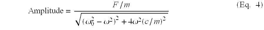
- Equation 4 This describes the commonly known frequency response for standard second order systems.
- Equation 5 has the form of the Mathieu equation, except that it has an added driving term on the right hand side.
- the equation displays parametric behavior, but it is coupled with a more traditional non-parametrically forced resonant behavior. Since damping raises the regions of instability within the parameter space, for small driving amplitudes in MEMS devices, the parametric instability is inaccessible, and the only response observed is the typical second order system response, a response illustrated at curve 150 in FIG. 16.
- Q is defined as the ratio between the frequency of peak amplitude and the bandwidth of the frequency response at the half-power points of the system.
- FIG. 16 shows the experimental frequency response. At a pressure of 10 mTorr, the device used to take the data in FIG. 16 had a Q of 1091.
- the dynamic behavior of a MEMS parametric oscillator is characterized by its various mechanical properties. For example, static out-of-plane deflection is extremely important, for it allows the experimental calculation of ⁇ , which is the torque versus angle of rotation slope parameter.
- the static actuator transfer function of displacement versus applied voltage is obtained by applying a wave form that consists of a combination of linear voltage ramps and constant voltages. This wave form may be applied at 1 Hz, to produce a series of displacement measurements at each point of the voltage ramp.
- An experimental static displacement curve 160 is illustrated in FIG. 17 In this figure, the dots illustrate experimental data while the solid line is a calculated shape. In the device used for this measurement, the movable beams were approximately 20 micrometers from the substrate and the supporting torsion bars were 25 micrometers long with each bar having a high aspect ratio, the bar being about 1.1 micrometer wide and 20 micrometers deep.
- resonant frequency of the device is the resonant frequency of the device, which can be determined in a number of ways. For example, a narrow pulse can be applied to the device and the frequency of its motion as it settles back to zero displacement is the natural frequency of the device. This can be measured using standard stroboscopic techniques. The stiffness of the device can be calculated from its dimensions, and the polar mass moment of inertia similarly can be calculated on the basis of the device dimensions.
- the natural resonant frequency of a parametric resonator such as the MEM device of FIG. 1 is ⁇ 0 , which is the center frequency of the instability region of the oscillator.
- the other frequencies which should cause instability can be calculated.
- the system can be driven near those frequencies, and with precise frequency control the unstable regions can be identified.
- These unstable regions are predicted by the Mathieu equations described above, have been experimentally observed, and are illustrated in FIG. 18 In this figure, the dots plot the frequency ratio ⁇ 0 / ⁇ for the experimentally observed instabilities, while the line 170 illustrates the theoretically-determined values.
- the center frequencies for the regions of instability are illustrated, and it was found that the instability frequencies matched the theoretical values to within 0.7%.
- FIG. 20 is an enlarged view of region 172 , which indicates that the boundary between stable and unstable regions are substantially linear.
- the instability regions, or tongues, illustrated in FIG. 19 can be mapped by initially selecting a drive signal having a frequency ⁇ and an amplitude ⁇ that produces resonance; that is produces an unstable excitation in the MEM device. By then maintaining a constant amplitude and varying the frequency in very small steps, the boundary between the stable and unstable regions can be determined. The amplitude of the drive signal is then changed and the process is As repeated.
- the instrumentation illustrated in FIG. 14 is used for this purpose, with the signal generator 182 supplying the desired drive signal under the control of computer 184 to the device 126 .
- FIGS. 23 and 24 illustrate the difference in amplitude of the MEM resonator in the stable and unstable regions.
- curve 190 in FIG. 23 illustrates the frequency and amplitude of the drive signal applied across the capacitor fingers of the resonant device 126 .
- Curve 192 is the output from vibrometer 122 , illustrating the displacement of the ends of the cantilever beam 12 (FIG. 1 ), for example at the location of tip 22 .
- curve 192 illustrates that the frequency and amplitude of the drive signal produces a high frequency and low amplitude response in the motion of the beam, thus indicating operation in a stable region.
- FIG. 24 illustrates a drive signal 194 having a slightly higher frequency than that illustrated in FIG. 23 which produces in the torsional oscillator 126 oscillation at a frequency 1 ⁇ 2 that of the drive frequency and with a relatively large amplitude, indicating unstable or resonant operation.
- the motion of the oscillator changes from a very low amplitude to a very large amplitude.
- resonators such as that illustrated in FIG. 1 can produce motion as great as ⁇ 8 micrometers when in the unstable region.
- the transition between stable and unstable regions is very different from a normal resonant excitation so that the values along the transition boundary, indicated by curve 180 in FIG. 22 is easily defined.
- the amplitude of motion is discontinuous at the transition frequency, with lower curve 202 representing amplitudes at frequencies which produce stable operation and curve 204 representing the amplitude of motion at frequencies which produce unstable, or resonant motion. In this operation, the dependence on the Q of the device is minimized.
- the boundary of the instability region has a number of useful properties.
- the motion of the oscillator is stable and its amplitude is small, and with damping, the motion decays to zero.
- the motion exhibits resonant excitation with high amplitude motion, and the boundary between the two is very sharp with changes in the drive signal frequency or the drive signal amplitude.
- the instability region differs from a standard resonant excitation in that with standard excitation, the transition between the stable and unstable regions is dependent on Q, and the growth in amplitude as well as the maximum amplitude are also determined by Q. In the Mathieu-based system, the amplitude and growth rates are not directly determined by Q.
- the amplitude of motion is essentially constant, as illustrated in FIG. 26 at curve 204 , with the amplitude being limited only by geometrical or material nonlinearities, and not by the damping present in the system. This is very useful for filter applications.
- the Q of the system was varied by changing the pressure in the testing environment, and the transition points between stable and unstable operation were mapped as described above.
- the mapping illustrated in FIG. 27 was carried out for pressures of 3T, 4.4T, 6,T and 10T, corresponding to changes in Q between 250 and 120.
- decreasing the vacuum level “rounds off” the bottom edge of the instability region, as illustrated at 206 , for example. This also has the effect of narrowing the instability region and with high enough damping, the transition region is rounded off and narrowed so completely that instability becomes inaccessible.
- One advantage of parametrically forced torsional resonance of the present invention is the use of this technique to reduce the parasitic signals in capacitive sensing in utilizing MEMS devices.
- the motion of many MEMS devices can be detected as changes in the capacitance between movable and fixed elements; such capacitive sensing is a major technique used for MEMS motion sensing.
- feedthrough currents which are the same frequency as the incoming excitation signal can occur. These feedthrough currents are referred to as parasitic signals, and can be large enough to overshadow the signals representing the capacitance change which is being detected.
- the capacitance change when the device is in motion is very small, due to the small number of movable fingers and the torsional motion. Since the capacitance between adjacent plates is proportional to the area between them, the change in capacitance in such devices is so small that standard capacitance detection techniques have trouble with stray signals.
- ⁇ 2 ⁇ 0 /n, or 114 kHz.
- the parasitic signals will be at the same frequency as the drive signal; namely, 114 kHz.
- the capacitive sensing signals of interest are also at 57 kHz. With this separation in frequency, it is straightforward to filter out the parasitic 114 kHz signal, thereby revealing the 57 kHz sensing signal. In this way, the frequency of interest is removed from the drive signal and allows capacitance detection techniques to be used even when small capacitance changes are being measured.
- Microelectromechanical filters are of increasing interest because of the ability to design structures that have a higher Q than is obtainable in electrical systems. These mechanical filters are also desirable because of their flexibility in frequency range.
- the sharp boundary provided by parametrically forced systems, as described above, enables parametrically forced structures to be used as filters and/or switches.
- the transition between a stable and an unstable operating condition in the MEMS of the present invention is extremely sharp, and occurs for a change in frequency of less than 0.001 Hz, according to measurements of experimental devices.
- this transition boundary operates as a very sensitive switch which can shift between stable and unstable conditions with changes in either voltage or frequency.
- operation of the device at a given frequency causes it to shift between stable and unstable conditions as the amplitude of the applied signal is varied; similarly, maintaining the drive signal at a given amplitude allows the device to be shifted between stable and unstable conditions by changing the frequency of the drive signal.
- Such switches have high discrimination between on and off signal levels.
- the device can be turned on with one voltage and turned off with a different voltage while holding the frequency constant, as illustrated along vertical line A in the figure. Similarly, by moving along line C in a horizontal direction, the device can be turned on with one frequency and off with another frequency while holding the applied voltage constant.
- the nonlinearities can be reduced by making torsional devices with stiffer springs which do not move as far out of plane, if desired.
- FIG. 28 illustrate how the MEM device of the invention can be used as a filter and/or a switch. Sweeping a range of frequencies while holding the amplitude constant shifts the device between stable and unstable conditions, with the bandwidth of the unstable condition being variable, depending upon the amplitude of the applied voltage.
- the sharp cutoff at the transitional boundaries, the bandwidth dependence on voltage, as well as a strong sensitivity to input frequencies provide a useful mechanical filter.
- Atomic force microscopy has been utilized for many years for a variety of applications, including imaging, but the sensing of very small forces. In such devices, it is extremely important to obtain a very high Q cantilever which is sensitive to its interaction with outside forces.
- Such cantilevers have atomically sharp tips, such as the tip 22 illustrated in FIG. 1, and accordingly the device of the present invention has significant application in this field. In such devices, sensitivity is obtained due to the fact that with high Q oscillators, small changes in the frequency of the oscillation due to force interaction with the sample can be sensed by measurable changes in amplitude of the vibration, since the force interaction in effect changes the stiffness of the oscillator.
- the cantilever of the present invention provides a highly sensitive atomic force microscopy.
- FIG. 29 is a schematic diagram of a parallel-plate actuator device, generally indicated at 220 , which includes fixed capacitor fingers 222 and 224 , and a movable actuator beam 226 carrying movable capacitor fingers 228 and 230 which are coplanar with, parallel to, and spaced from corresponding fixed fingers.
- the actuator beam is supported at opposite ends by spring arms 232 and 234 which allow the actuator beam to move in the plane of the beam and along its longitudinal axis.
- the springs 232 and 234 preferably are mounted at their outer ends to the fixed substrate which supports the fixed fingers.
- the fixed and movable fingers carry electrically conductive layers forming capacitor plates on their opposed faces.
- the force law for a parallel plate actuator such as actuator 220 has parametric terms which affect the dynamic behavior of the system.
- the resultant motion of the system thus may be governed by parametric terms and does not display the behavior expected from a single constant-coefficient equation model.
- the parametric forcing in a dynamically forced MEMS parallel plate actuator is ⁇ 10 5 larger than the external forcing. Simulations of this equation show that for external forcing 10 5 less than the parametric forcing, the equation still displays parametric resonance behavior when excited in the first instability region, as predicted from the linear theory of the Mathieu Equation.
- the response is a parametric one, based on the frequency of the output.
- FIGS. 31 and 32 illustrate this.
- Curve 242 in FIG. 31 shows the response of a system with no parametric driving. The only forcing term is an external one. This system displays input typical of a standard resonator, and the amplitude grows linearly.
- Curve 244 in FIG. 32 shows the same amplitude driving term, but has an additional parametric driving term ten times larger than the external term. From this addition, it is seen that the response is now being dominated by the parametric forcing, for it displays the exponential growth associated with parametric excitation.
- the actuator 250 includes a reduction actuator 252 and an augmentation actuator 254 which resemble comb drive actuators, except that their stationary fingers 256 and 258 are not interdigitated with the corresponding movable fingers 260 and 262 , respectively, mounted on movable beam 264 .
- the reduction actuator 252 configuration when the actuator beam 264 moves to the left, the net force toward the left is increased, while in the augmentation actuator 254 configuration, when the actuator beam 264 moves to the left, the net electrostatic force is toward the right.
- These actuators unlike standard comb-drive actuators, move in a direction that is perpendicular to the direction of the fingers, as shown schematically by arrow 266 in the figure. They move because of the fringing electric fields between the movable and fixed fingers.
- FIG. 34 is a graph including a curve 280 showing force vs. displacement for different regions of the force relation for reduction/augmentation actuators.
- the open squares represent the centers of the reduction areas.
- the stiffness due to the electrostatic changes sign. Note that there is no force generated when the fingers are in the center, or zero displacement, position.
- FIG. 34 Examination of FIG. 34 reveals two distinct linear regions. In the region surrounding points marked by the open squares, the curve has a negative slope (augmentation), and for the region surrounding points marked by open circles (reduction), the curve has a positive slope. Thus, depending on the initial position of the actuator, the behavior of the device can be quite different.
- the reduction actuator has the same form as Equation 15, except the sign is reversed on the term proceeding x due to electrostatic forcing.
- FIG. 35 One additional device which shows parametric resonance is a linear-force comb actuator such as that illustrated at 290 in FIG. 35 .
- This comb drive is very similar to a standard in-plane comb drive; however, this comb drive has fingers which vary in length.
- a schematic of such a device is shown in FIG. 35 .
- a movable beam 292 is mounted at its opposite ends on springs 294 and 296 , which are perpendicular to the axis of beam 292 .
- the springs are fixed at their outer ends to constrain the beam to linear motion along its axis, in the direction of arrow 298 .
- the beam carries movable sets 300 , 302 , 304 , and 306 of fingers 310 which oppose corresponding fixed sets 312 , 314 , 316 , and 318 of fingers 320 , mounted, for example, on a substrate.
- the lengths of the fixed fingers 320 vary linearly along each set.
- the first instability region displays parametric actuation as explained with respect to the parallel plate actuator.
- the non-parametric driving term is at the same frequency as the region of parametric instability. So if Iq is large, the term on the right-hand side of the equation dominates and the response is not parametric in nature. However, if Iq is very small, then the parametric response dominates the behavior. Numerical studies have shown that ifs s>5q (the parametric term is >5 times larger than the external driving term), then the parametric terms dominate the response.
- the ideal configuration would be one in which the force generated in the starting position is very small, and as the actuator moves in either direction, the force increases linearly.
- Microelectromechanical actuator configurations such as those described above, as well as other configurations which may be operated parametrically to achieve resonance at frequencies other than the natural frequency of the device, have a wide range of uses.
- the nonlinear or quasi-linear effect produced by the sharp discontinuity between stable and unstable operation due to changes in the properties of the device can be used in a wide variety of sensing applications. For example, very small changes in temperature, pressure, force, mass, damping, or the like can cause a parametric actuator to cross the threshold between stable and unstable operation. This shift produces a large change in the output of the actuator at a characteristic frequency that is easy to detect, as has been described.
- a parallel-plate capacitive actuator such as that illustrated in FIG. 29, can be used as a parametric mass sensor.
- k is the linear stiffness of the system
- m is the mass
- ⁇ 0 is the permittivity of the fluid in which the device is operated in
- d is the gap between fixed and moving actuator plates
- ⁇ driving frequency
- A is the area of the capacitive plate
- a DC is the applied signal magnitude.
- ⁇ m ⁇ ( 4 ⁇ k - 4 ⁇ ⁇ ⁇ 0 ⁇ A ⁇ ⁇ A DC d 0 3 ⁇ ⁇ 1 ⁇ 3 ) ⁇ ⁇ ⁇ ⁇ ⁇ ( Eq . ⁇ 21 )
Abstract
Description


Claims (34)
Priority Applications (1)
| Application Number | Priority Date | Filing Date | Title |
|---|---|---|---|
| US09/586,976 US6497141B1 (en) | 1999-06-07 | 2000-06-05 | Parametric resonance in microelectromechanical structures |
Applications Claiming Priority (2)
| Application Number | Priority Date | Filing Date | Title |
|---|---|---|---|
| US13812599P | 1999-06-07 | 1999-06-07 | |
| US09/586,976 US6497141B1 (en) | 1999-06-07 | 2000-06-05 | Parametric resonance in microelectromechanical structures |
Publications (1)
| Publication Number | Publication Date |
|---|---|
| US6497141B1 true US6497141B1 (en) | 2002-12-24 |
Family
ID=26835887
Family Applications (1)
| Application Number | Title | Priority Date | Filing Date |
|---|---|---|---|
| US09/586,976 Expired - Fee Related US6497141B1 (en) | 1999-06-07 | 2000-06-05 | Parametric resonance in microelectromechanical structures |
Country Status (1)
| Country | Link |
|---|---|
| US (1) | US6497141B1 (en) |
Cited By (101)
| Publication number | Priority date | Publication date | Assignee | Title |
|---|---|---|---|---|
| US20020162947A1 (en) * | 2001-04-12 | 2002-11-07 | Weitekamp Daniel P. | Mechanical sensors of electromagnetic fields |
| WO2003050889A1 (en) * | 2001-12-10 | 2003-06-19 | Abu-Ageel Nayef M | Micro-machine electrostatic actuator, method and system employing same, and fabrication methods thereof |
| US20030123124A1 (en) * | 2001-12-10 | 2003-07-03 | Abu-Ageel Nayef M. | Micro-machine electrostatic actuator, method and system employing same, and fabrication methods thereof |
| US6617750B2 (en) * | 1999-09-21 | 2003-09-09 | Rockwell Automation Technologies, Inc. | Microelectricalmechanical system (MEMS) electrical isolator with reduced sensitivity to inertial noise |
| US20030173864A1 (en) * | 2002-03-12 | 2003-09-18 | Maxim Zalalutdinov | Heat pumped parametric MEMS device |
| US6664786B2 (en) | 2001-07-30 | 2003-12-16 | Rockwell Automation Technologies, Inc. | Magnetic field sensor using microelectromechanical system |
| US6686639B1 (en) * | 2002-09-30 | 2004-02-03 | Innovative Technology Licensing, Llc | High performance MEMS device fabricatable with high yield |
| US20040021403A1 (en) * | 2002-08-01 | 2004-02-05 | Georgia Tech Research Corporation | Piezoelectric on semiconductor-on-insulator microelectromechanical resonators and methods of fabrication |
| US6690178B2 (en) | 2001-10-26 | 2004-02-10 | Rockwell Automation Technologies, Inc. | On-board microelectromechanical system (MEMS) sensing device for power semiconductors |
| US6710680B2 (en) * | 2001-12-20 | 2004-03-23 | Motorola, Inc. | Reduced size, low loss MEMS torsional hinges and MEMS resonators employing such hinges |
| US20040065940A1 (en) * | 2002-08-07 | 2004-04-08 | Farrokh Ayazi | Capacitive resonators and methods of fabrication |
| US6756310B2 (en) | 2001-09-26 | 2004-06-29 | Rockwell Automation Technologies, Inc. | Method for constructing an isolate microelectromechanical system (MEMS) device using surface fabrication techniques |
| US6761829B2 (en) | 2001-04-26 | 2004-07-13 | Rockwell Automation Technologies, Inc. | Method for fabricating an isolated microelectromechanical system (MEMS) device using an internal void |
| US6768628B2 (en) | 2001-04-26 | 2004-07-27 | Rockwell Automation Technologies, Inc. | Method for fabricating an isolated microelectromechanical system (MEMS) device incorporating a wafer level cap |
| US6794271B2 (en) | 2001-09-28 | 2004-09-21 | Rockwell Automation Technologies, Inc. | Method for fabricating a microelectromechanical system (MEMS) device using a pre-patterned bridge |
| US6798312B1 (en) | 1999-09-21 | 2004-09-28 | Rockwell Automation Technologies, Inc. | Microelectromechanical system (MEMS) analog electrical isolator |
| US20040189142A1 (en) * | 2003-03-25 | 2004-09-30 | Knieser Michael J. | Microelectromechanical isolating circuit |
| US6803755B2 (en) | 1999-09-21 | 2004-10-12 | Rockwell Automation Technologies, Inc. | Microelectromechanical system (MEMS) with improved beam suspension |
| US6815243B2 (en) | 2001-04-26 | 2004-11-09 | Rockwell Automation Technologies, Inc. | Method of fabricating a microelectromechanical system (MEMS) device using a pre-patterned substrate |
| US20040232502A1 (en) * | 2003-05-06 | 2004-11-25 | Walsin Lihwa Corporation | High-aspect-ratio-microstructure (HARM) |
| WO2005011071A2 (en) * | 2003-07-28 | 2005-02-03 | Technion Research And Development Foundation Ltd. | Vertical comb drive and uses thereof |
| US20050067901A1 (en) * | 2003-09-30 | 2005-03-31 | Harris Richard D. | Microelectromechanical isolating power converter |
| US20050126295A1 (en) * | 2003-11-07 | 2005-06-16 | Raffaele Correale | Pressure sensor |
| US20050151592A1 (en) * | 2004-01-09 | 2005-07-14 | Aaron Partridge | Frequency and/or phase compensated microelectromechanical oscillator |
| US20050156481A1 (en) * | 2004-01-20 | 2005-07-21 | Guangya Zhou | Optical scanning using vibratory diffraction gratings |
| US20050162811A1 (en) * | 2004-01-26 | 2005-07-28 | Yamaichi Electronics Co., Ltd. | Comb-shaped actuator |
| US20050174624A1 (en) * | 2004-02-05 | 2005-08-11 | Greywall Dennis S. | MEMS actuator for piston and tilt motion |
| US20050200938A1 (en) * | 2004-03-09 | 2005-09-15 | Greywall Dennis S. | MEMS device for an adaptive optics mirror |
| US20050252293A1 (en) * | 2004-05-11 | 2005-11-17 | Samsung Electronics Co., Ltd. | Magnetic MEMS device and method of forming thereof |
| WO2005116621A2 (en) * | 2004-05-25 | 2005-12-08 | The Government Of The United States Of America, As Represented By The Secretary Of The Navy Naval Research Laboratory | Microelectro-mechanical chemical sensor |
| US20060157807A1 (en) * | 2002-06-27 | 2006-07-20 | Cornell Research Foundation, Inc. | Three dimensional high aspect ratio micromachining |
| US20060185433A1 (en) * | 2005-02-18 | 2006-08-24 | Honeywell International, Inc. | MEMS teeter-totter accelerometer having reduced non-linearty |
| US20060204242A1 (en) * | 2005-02-28 | 2006-09-14 | Gutierrez Roman C | Autofocus camera |
| US20060267596A1 (en) * | 2003-05-21 | 2006-11-30 | The Secretary Of State For Trade And Industry Of Her Majesty's Britannic Government | Spring constant calibration device |
| US20070046397A1 (en) * | 2005-08-01 | 2007-03-01 | Purdue Research Foundation | Nonlinear internal resonance based micromechanical resonators |
| US20070176701A1 (en) * | 2006-01-31 | 2007-08-02 | Matsushita Electric Industrial Co., Ltd. | Parametric resonator and filter using the same |
| US20070200648A1 (en) * | 2005-11-09 | 2007-08-30 | Cornell Research Foundation, Inc. | MEMS controlled oscillator |
| US20070228869A1 (en) * | 2006-03-31 | 2007-10-04 | Aksyuk Vladimir A | Stable electro-mechanical actuators |
| US20080013140A1 (en) * | 2003-12-25 | 2008-01-17 | Canon Kabushiki Kaisha | Micro-oscillating member, light-deflector, and image-forming apparatus |
| US20080011044A1 (en) * | 2006-07-17 | 2008-01-17 | Workman Richard K | Force method for Determining the Spring Constant of Scanning Probe Microscope Cantilevers using MEMS Actuators |
| US20080047346A1 (en) * | 2005-08-01 | 2008-02-28 | Ashwin Vyas | Nonlinear micromechanical resonator |
| US20080106169A1 (en) * | 2006-11-06 | 2008-05-08 | Sony Corporation | Actuation device |
| CN100434882C (en) * | 2007-11-20 | 2008-11-19 | 东南大学 | Static excitation resonator capacitor vibration pick-up structure |
| US20090218909A1 (en) * | 2003-08-12 | 2009-09-03 | Fujitsu Limited | Micro-oscillation element and method for driving the same |
| US20100038753A1 (en) * | 2008-08-13 | 2010-02-18 | Oki Semiconductor Co., Ltd. | Variable capacitor employing MEMS technology |
| US20100052597A1 (en) * | 2008-09-04 | 2010-03-04 | Dong Jingyan | Displacement actuation and sensing for an electrostatic drive |
| US20100109579A1 (en) * | 2008-10-30 | 2010-05-06 | Walmsley Robert G | Resonator having a stator coupled to three stator voltages |
| US20110041224A1 (en) * | 2009-08-06 | 2011-02-17 | Purdue Research Foundation | Atomic force microscope including accelerometer |
| US20110049092A1 (en) * | 2009-08-26 | 2011-03-03 | Alfred I-Tsung Pan | Inkjet printhead bridge beam fabrication method |
| US20110102105A1 (en) * | 2009-11-02 | 2011-05-05 | Harris Corporation | Mems-based tunable filter |
| US20110188168A1 (en) * | 2010-02-03 | 2011-08-04 | Harris Corporation | High accuracy mems-based varactors |
| US20110198202A1 (en) * | 2010-02-18 | 2011-08-18 | Harris Corporation | Mems-based ultra-low power devices |
| US20110221454A1 (en) * | 2008-06-11 | 2011-09-15 | Analog Devices, Inc. | Anti-Capture Method and Apparatus for Micromachined Devices |
| US20110260810A1 (en) * | 2008-07-29 | 2011-10-27 | Quevy Emmanuel P | Out-of-plane mems resonator with static out-of-plane deflection |
| WO2012005756A1 (en) * | 2010-06-29 | 2012-01-12 | Headway Technologies, Inc | Drive method for starting and operating a resonant scanning mems device at its resonant frequency |
| US8337103B2 (en) | 2010-11-15 | 2012-12-25 | DigitalOptics Corporation MEMS | Long hinge actuator snubbing |
| US8358925B2 (en) | 2010-11-15 | 2013-01-22 | DigitalOptics Corporation MEMS | Lens barrel with MEMS actuators |
| US8372677B2 (en) | 2006-05-10 | 2013-02-12 | Qualtre, Inc. | Three-axis accelerometers and fabrication methods |
| US8430580B2 (en) | 2010-11-15 | 2013-04-30 | DigitalOptics Corporation MEMS | Rotationally deployed actuators |
| CN103183305A (en) * | 2012-01-03 | 2013-07-03 | 探微科技股份有限公司 | Comb-shaped electrode structure |
| US8521017B2 (en) | 2010-11-15 | 2013-08-27 | DigitalOptics Corporation MEMS | MEMS actuator alignment |
| US8547627B2 (en) | 2010-11-15 | 2013-10-01 | DigitalOptics Corporation MEMS | Electrical routing |
| US8571405B2 (en) | 2011-09-28 | 2013-10-29 | DigitalOptics Corporation MEMS | Surface mount actuator |
| US8604663B2 (en) | 2010-11-15 | 2013-12-10 | DigitalOptics Corporation MEMS | Motion controlled actuator |
| US8605375B2 (en) | 2010-11-15 | 2013-12-10 | DigitalOptics Corporation MEMS | Mounting flexure contacts |
| US8608393B2 (en) | 2010-11-15 | 2013-12-17 | DigitalOptics Corporation MEMS | Capillary actuator deployment |
| US8616791B2 (en) | 2011-09-28 | 2013-12-31 | DigitalOptics Corporation MEMS | Rotationally deployed actuator devices |
| US8619378B2 (en) | 2010-11-15 | 2013-12-31 | DigitalOptics Corporation MEMS | Rotational comb drive Z-stage |
| US8637961B2 (en) | 2010-11-15 | 2014-01-28 | DigitalOptics Corporation MEMS | MEMS actuator device |
| US20140028192A1 (en) * | 2012-07-25 | 2014-01-30 | Infineon Technologies Ag | Field Emission Devices and Methods of Making Thereof |
| US8674775B2 (en) | 2011-06-30 | 2014-03-18 | Silicon Laboratories Inc. | Out-of-plane resonator |
| US8752211B2 (en) * | 2012-08-03 | 2014-06-10 | Ut-Battelle, Llc | Real space mapping of oxygen vacancy diffusion and electrochemical transformations by hysteretic current reversal curve measurements |
| US8768157B2 (en) | 2011-09-28 | 2014-07-01 | DigitalOptics Corporation MEMS | Multiple degree of freedom actuator |
| US8803256B2 (en) | 2010-11-15 | 2014-08-12 | DigitalOptics Corporation MEMS | Linearly deployed actuators |
| US8853975B2 (en) | 2011-09-28 | 2014-10-07 | DigitalOptics Corporation MEMS | Electrostatic actuator control |
| US8855476B2 (en) | 2011-09-28 | 2014-10-07 | DigitalOptics Corporation MEMS | MEMS-based optical image stabilization |
| US8869625B2 (en) | 2011-09-28 | 2014-10-28 | DigitalOptics Corporation MEMS | MEMS actuator/sensor |
| US8884381B2 (en) | 2010-11-15 | 2014-11-11 | DigitalOptics Corporation MEMS | Guard trench |
| WO2014200606A2 (en) * | 2013-04-14 | 2014-12-18 | Purdue Research Foundation | Performance improvement of mems devices |
| US8941192B2 (en) | 2010-11-15 | 2015-01-27 | DigitalOptics Corporation MEMS | MEMS actuator device deployment |
| US9019390B2 (en) | 2011-09-28 | 2015-04-28 | DigitalOptics Corporation MEMS | Optical image stabilization using tangentially actuated MEMS devices |
| US9032797B2 (en) | 2011-02-11 | 2015-05-19 | Fraunhofer-Gesellschaft Zur Foerderung Der Angewandten Forschung E.V. | Sensor device and method |
| US20150145531A1 (en) * | 2013-11-26 | 2015-05-28 | Li Lin | Method, system and apparatus for capacitive sensing |
| US9052567B2 (en) | 2010-11-15 | 2015-06-09 | DigitalOptics Corporation MEMS | Actuator inside of motion control |
| US9061883B2 (en) | 2010-11-15 | 2015-06-23 | DigitalOptics Corporation MEMS | Actuator motion control features |
| US9063278B2 (en) | 2010-11-15 | 2015-06-23 | DigitalOptics Corporation MEMS | Miniature MEMS actuator assemblies |
| US9093975B2 (en) | 2013-08-19 | 2015-07-28 | Harris Corporation | Microelectromechanical systems comprising differential inductors and methods for making the same |
| US9123493B2 (en) | 2014-01-23 | 2015-09-01 | Harris Corporation | Microelectromechanical switches for steering of RF signals |
| US9136822B2 (en) | 2013-08-19 | 2015-09-15 | Harris Corporation | Microelectromechanical system with a micro-scale spring suspension system and methods for making the same |
| US9172352B2 (en) | 2013-08-19 | 2015-10-27 | Harris Corporation | Integrated microelectromechanical system devices and methods for making the same |
| US9281763B2 (en) | 2011-09-28 | 2016-03-08 | DigitalOptics Corporation MEMS | Row and column actuator control |
| US20160072472A1 (en) * | 2014-02-20 | 2016-03-10 | Carnegie Mellon University, A Pennsylvania Non-Profit Corporation | Method and device for bi-state control of nonlinear resonators |
| US9350271B2 (en) | 2011-09-28 | 2016-05-24 | DigitalOptics Corporation MEMS | Cascaded electrostatic actuator |
| US9352962B2 (en) | 2010-11-15 | 2016-05-31 | DigitalOptics Corporation MEMS | MEMS isolation structures |
| US9515579B2 (en) | 2010-11-15 | 2016-12-06 | Digitaloptics Corporation | MEMS electrical contact systems and methods |
| EP3171145A1 (en) * | 2015-11-23 | 2017-05-24 | ETH Zurich | Method and sensor for measuring small forces |
| US9970764B2 (en) | 2009-08-31 | 2018-05-15 | Georgia Tech Research Corporation | Bulk acoustic wave gyroscope with spoked structure |
| CN108061966A (en) * | 2017-12-11 | 2018-05-22 | 无锡英菲感知技术有限公司 | A kind of micro mirror for having both translation and rotation work pattern |
| CN109855791A (en) * | 2018-11-21 | 2019-06-07 | 中国计量大学 | Vacuum detecting device based on more folded beam comb teeth resonators |
| CN109879239A (en) * | 2019-01-23 | 2019-06-14 | 西安交通大学 | A kind of micro- resonance pressure sensor chip of double H-type strut-beam silicon and preparation method thereof |
| DE102022200335A1 (en) | 2022-01-13 | 2023-07-13 | Robert Bosch Gesellschaft mit beschränkter Haftung | Sensor system and method for determining a change in capacitance per unit length |
Citations (15)
| Publication number | Priority date | Publication date | Assignee | Title |
|---|---|---|---|---|
| GB2101336A (en) * | 1981-07-02 | 1983-01-12 | Centre Electron Horloger | Capacitive accelerometers |
| US4472239A (en) | 1981-10-09 | 1984-09-18 | Honeywell, Inc. | Method of making semiconductor device |
| US4918032A (en) | 1988-04-13 | 1990-04-17 | General Motors Corporation | Method for fabricating three-dimensional microstructures and a high-sensitivity integrated vibration sensor using such microstructures |
| WO1992003740A1 (en) | 1990-08-17 | 1992-03-05 | Analog Devices, Inc. | Monolithic accelerometer |
| EP0480471A2 (en) | 1990-10-12 | 1992-04-15 | OKADA, Kazuhiro | Force detector and acceleration detector and method of manufacturing the same |
| US5198390A (en) | 1992-01-16 | 1993-03-30 | Cornell Research Foundation, Inc. | RIE process for fabricating submicron, silicon electromechanical structures |
| US5211051A (en) | 1987-11-09 | 1993-05-18 | California Institute Of Technology | Methods and apparatus for improving sensor performance |
| EP0567938A1 (en) | 1992-04-30 | 1993-11-03 | Texas Instruments Incorporated | Digital accelerometer |
| US5393375A (en) | 1992-02-03 | 1995-02-28 | Cornell Research Foundation, Inc. | Process for fabricating submicron single crystal electromechanical structures |
| EP0665590A2 (en) | 1994-01-31 | 1995-08-02 | Canon Kabushiki Kaisha | Microstructure, process for manufacturing thereof and devices incorporating the same |
| EP0703429A2 (en) | 1994-09-21 | 1996-03-27 | Canon Kabushiki Kaisha | Probe with torsion lever structure, and scanning probe microscope and record/reproducing apparatus utilizing the same |
| US5719073A (en) | 1993-02-04 | 1998-02-17 | Cornell Research Foundation, Inc. | Microstructures and single mask, single-crystal process for fabrication thereof |
| US5914553A (en) | 1997-06-16 | 1999-06-22 | Cornell Research Foundation, Inc. | Multistable tunable micromechanical resonators |
| US6000280A (en) | 1995-07-20 | 1999-12-14 | Cornell Research Foundation, Inc. | Drive electrodes for microfabricated torsional cantilevers |
| US6073484A (en) | 1995-07-20 | 2000-06-13 | Cornell Research Foundation, Inc. | Microfabricated torsional cantilevers for sensitive force detection |
-
2000
- 2000-06-05 US US09/586,976 patent/US6497141B1/en not_active Expired - Fee Related
Patent Citations (16)
| Publication number | Priority date | Publication date | Assignee | Title |
|---|---|---|---|---|
| GB2101336A (en) * | 1981-07-02 | 1983-01-12 | Centre Electron Horloger | Capacitive accelerometers |
| US4472239A (en) | 1981-10-09 | 1984-09-18 | Honeywell, Inc. | Method of making semiconductor device |
| US5211051A (en) | 1987-11-09 | 1993-05-18 | California Institute Of Technology | Methods and apparatus for improving sensor performance |
| US4918032A (en) | 1988-04-13 | 1990-04-17 | General Motors Corporation | Method for fabricating three-dimensional microstructures and a high-sensitivity integrated vibration sensor using such microstructures |
| WO1992003740A1 (en) | 1990-08-17 | 1992-03-05 | Analog Devices, Inc. | Monolithic accelerometer |
| EP0480471A2 (en) | 1990-10-12 | 1992-04-15 | OKADA, Kazuhiro | Force detector and acceleration detector and method of manufacturing the same |
| US5198390A (en) | 1992-01-16 | 1993-03-30 | Cornell Research Foundation, Inc. | RIE process for fabricating submicron, silicon electromechanical structures |
| US5393375A (en) | 1992-02-03 | 1995-02-28 | Cornell Research Foundation, Inc. | Process for fabricating submicron single crystal electromechanical structures |
| EP0567938A1 (en) | 1992-04-30 | 1993-11-03 | Texas Instruments Incorporated | Digital accelerometer |
| US5719073A (en) | 1993-02-04 | 1998-02-17 | Cornell Research Foundation, Inc. | Microstructures and single mask, single-crystal process for fabrication thereof |
| US6051866A (en) | 1993-02-04 | 2000-04-18 | Cornell Research Foundation, Inc. | Microstructures and single mask, single-crystal process for fabrication thereof |
| EP0665590A2 (en) | 1994-01-31 | 1995-08-02 | Canon Kabushiki Kaisha | Microstructure, process for manufacturing thereof and devices incorporating the same |
| EP0703429A2 (en) | 1994-09-21 | 1996-03-27 | Canon Kabushiki Kaisha | Probe with torsion lever structure, and scanning probe microscope and record/reproducing apparatus utilizing the same |
| US6000280A (en) | 1995-07-20 | 1999-12-14 | Cornell Research Foundation, Inc. | Drive electrodes for microfabricated torsional cantilevers |
| US6073484A (en) | 1995-07-20 | 2000-06-13 | Cornell Research Foundation, Inc. | Microfabricated torsional cantilevers for sensitive force detection |
| US5914553A (en) | 1997-06-16 | 1999-06-22 | Cornell Research Foundation, Inc. | Multistable tunable micromechanical resonators |
Non-Patent Citations (5)
| Title |
|---|
| Grigg, D.A., Russell, P.E.& Griffith, J.E.; Rocking-beam force-balance approach to atomic force microscopy; Ultramicroscopy 42-44, (1992); Amsterdam, NL; pp. 1504-1508. |
| Miller, Scott A.; Turner, Kimberly L.; MacDonald,Noel C.; Microelectromechanical scanning probe instruments for array architectures; Rev. Sci. Instrum. 68(11), Nov. 1997, pp. 4155-4162. |
| Tang, W.C. et al., "Electrostatic Comb Drive Levitation and Control Method", Journal of Microelectromechanical Systems, vol. 1, No. 4, Dec. 1992, pp. 170-178.* * |
| Xu, Y. et al., "Integrated Micro-Scanning Tunneling Microscope", Appl. Phys. Lett., vol. 67, No. 16, Oct. 16, 1995, pp. 2305-2307.* * |
| Xu, Y. et al., "Microelectromechanical Scanning Tunneling Microscope", Transducers '95-Eurosensors IX, the 8th International Conference on Solid-State Sensors and Acutators, and Eurosensors IX, Jun. 25-Jun. 29, 1995, pp. 640-643.* * |
Cited By (180)
| Publication number | Priority date | Publication date | Assignee | Title |
|---|---|---|---|---|
| US6803755B2 (en) | 1999-09-21 | 2004-10-12 | Rockwell Automation Technologies, Inc. | Microelectromechanical system (MEMS) with improved beam suspension |
| US6617750B2 (en) * | 1999-09-21 | 2003-09-09 | Rockwell Automation Technologies, Inc. | Microelectricalmechanical system (MEMS) electrical isolator with reduced sensitivity to inertial noise |
| US6798312B1 (en) | 1999-09-21 | 2004-09-28 | Rockwell Automation Technologies, Inc. | Microelectromechanical system (MEMS) analog electrical isolator |
| US6835926B2 (en) * | 2001-04-12 | 2004-12-28 | California Institute Of Technology | Mechanical sensors of electromagnetic fields |
| US20020162947A1 (en) * | 2001-04-12 | 2002-11-07 | Weitekamp Daniel P. | Mechanical sensors of electromagnetic fields |
| US6761829B2 (en) | 2001-04-26 | 2004-07-13 | Rockwell Automation Technologies, Inc. | Method for fabricating an isolated microelectromechanical system (MEMS) device using an internal void |
| US7387737B2 (en) | 2001-04-26 | 2008-06-17 | Rockwell Automation Technologies, Inc. | Method for fabricating an isolated microelectromechanical system (MEMS) device using an internal void |
| US6815243B2 (en) | 2001-04-26 | 2004-11-09 | Rockwell Automation Technologies, Inc. | Method of fabricating a microelectromechanical system (MEMS) device using a pre-patterned substrate |
| US7018550B2 (en) | 2001-04-26 | 2006-03-28 | Rockwell Automation Technologies, Inc. | Method for fabricating an isolated microelectromechanical system (MEMS) device using an internal void |
| US6768628B2 (en) | 2001-04-26 | 2004-07-27 | Rockwell Automation Technologies, Inc. | Method for fabricating an isolated microelectromechanical system (MEMS) device incorporating a wafer level cap |
| US20040262257A1 (en) * | 2001-04-26 | 2004-12-30 | Harris Richard D. | Method for fabricating an isolated microelectromechanical system (MEMS) device using an internal void |
| US6664786B2 (en) | 2001-07-30 | 2003-12-16 | Rockwell Automation Technologies, Inc. | Magnetic field sensor using microelectromechanical system |
| US6756310B2 (en) | 2001-09-26 | 2004-06-29 | Rockwell Automation Technologies, Inc. | Method for constructing an isolate microelectromechanical system (MEMS) device using surface fabrication techniques |
| US6846724B2 (en) | 2001-09-28 | 2005-01-25 | Rockwell Automation Technologies, Inc. | Method for fabricating a microelectromechanical system (MEMS) device using a pre-patterned bridge |
| US6794271B2 (en) | 2001-09-28 | 2004-09-21 | Rockwell Automation Technologies, Inc. | Method for fabricating a microelectromechanical system (MEMS) device using a pre-patterned bridge |
| US20040209413A1 (en) * | 2001-09-28 | 2004-10-21 | Harris Richard D. | Method for fabricating a microelectromechanical system (MEMS) device using a pre-patterned bridge |
| US6690178B2 (en) | 2001-10-26 | 2004-02-10 | Rockwell Automation Technologies, Inc. | On-board microelectromechanical system (MEMS) sensing device for power semiconductors |
| US6757092B2 (en) * | 2001-12-10 | 2004-06-29 | Nayef M. Abu-Ageel | Micro-machine electrostatic actuator, method and system employing same, and fabrication methods thereof |
| US20030123124A1 (en) * | 2001-12-10 | 2003-07-03 | Abu-Ageel Nayef M. | Micro-machine electrostatic actuator, method and system employing same, and fabrication methods thereof |
| WO2003050889A1 (en) * | 2001-12-10 | 2003-06-19 | Abu-Ageel Nayef M | Micro-machine electrostatic actuator, method and system employing same, and fabrication methods thereof |
| US6710680B2 (en) * | 2001-12-20 | 2004-03-23 | Motorola, Inc. | Reduced size, low loss MEMS torsional hinges and MEMS resonators employing such hinges |
| US20030173864A1 (en) * | 2002-03-12 | 2003-09-18 | Maxim Zalalutdinov | Heat pumped parametric MEMS device |
| US7654140B2 (en) * | 2002-03-12 | 2010-02-02 | Cornell Research Foundation, Inc. | Heat pumped parametric MEMS device |
| US7504757B2 (en) * | 2002-06-27 | 2009-03-17 | Cornell Research Foundation, Inc. | Multi-finger z-actuator |
| US20060157807A1 (en) * | 2002-06-27 | 2006-07-20 | Cornell Research Foundation, Inc. | Three dimensional high aspect ratio micromachining |
| US6909221B2 (en) | 2002-08-01 | 2005-06-21 | Georgia Tech Research Corporation | Piezoelectric on semiconductor-on-insulator microelectromechanical resonators |
| US20040021403A1 (en) * | 2002-08-01 | 2004-02-05 | Georgia Tech Research Corporation | Piezoelectric on semiconductor-on-insulator microelectromechanical resonators and methods of fabrication |
| US7023065B2 (en) | 2002-08-07 | 2006-04-04 | Georgia Tech Research Corporation | Capacitive resonators and methods of fabrication |
| US20040065940A1 (en) * | 2002-08-07 | 2004-04-08 | Farrokh Ayazi | Capacitive resonators and methods of fabrication |
| US20060273416A1 (en) * | 2002-08-07 | 2006-12-07 | Farrokh Ayazi | Capacitive resonators |
| US6686639B1 (en) * | 2002-09-30 | 2004-02-03 | Innovative Technology Licensing, Llc | High performance MEMS device fabricatable with high yield |
| US6975193B2 (en) | 2003-03-25 | 2005-12-13 | Rockwell Automation Technologies, Inc. | Microelectromechanical isolating circuit |
| US20040189142A1 (en) * | 2003-03-25 | 2004-09-30 | Knieser Michael J. | Microelectromechanical isolating circuit |
| US7088030B2 (en) * | 2003-05-06 | 2006-08-08 | Walsin Lihwa Corporation | High-aspect-ratio-microstructure (HARM) |
| US20040232502A1 (en) * | 2003-05-06 | 2004-11-25 | Walsin Lihwa Corporation | High-aspect-ratio-microstructure (HARM) |
| US20060267596A1 (en) * | 2003-05-21 | 2006-11-30 | The Secretary Of State For Trade And Industry Of Her Majesty's Britannic Government | Spring constant calibration device |
| WO2005011071A3 (en) * | 2003-07-28 | 2006-01-26 | Technion Res & Dev Foundation | Vertical comb drive and uses thereof |
| US20080197748A1 (en) * | 2003-07-28 | 2008-08-21 | Technion Research And Development Foundation Ltd. | Vertical Comb Drive and Uses Thereof |
| WO2005011071A2 (en) * | 2003-07-28 | 2005-02-03 | Technion Research And Development Foundation Ltd. | Vertical comb drive and uses thereof |
| US20090218909A1 (en) * | 2003-08-12 | 2009-09-03 | Fujitsu Limited | Micro-oscillation element and method for driving the same |
| US7701155B2 (en) * | 2003-08-12 | 2010-04-20 | Fujitsu Limited | Method for driving micro-oscillating element having comb-teeth electrodes |
| US7262522B2 (en) * | 2003-09-30 | 2007-08-28 | Rockwell Automation Technologies, Inc. | Microelectromechanical isolating power converter |
| US20050067901A1 (en) * | 2003-09-30 | 2005-03-31 | Harris Richard D. | Microelectromechanical isolating power converter |
| US7059192B2 (en) * | 2003-11-07 | 2006-06-13 | Varian S.P.A. | Pressure sensor |
| US20050126295A1 (en) * | 2003-11-07 | 2005-06-16 | Raffaele Correale | Pressure sensor |
| US7643198B2 (en) | 2003-12-25 | 2010-01-05 | Canon Kabushiki Kaisha | Micro-oscillating member, light-deflector, and image-forming apparatus |
| US7388702B2 (en) * | 2003-12-25 | 2008-06-17 | Canon Kabushiki Kaisha | Micro-oscillating member, light-deflector, and image-forming apparatus |
| US20080013140A1 (en) * | 2003-12-25 | 2008-01-17 | Canon Kabushiki Kaisha | Micro-oscillating member, light-deflector, and image-forming apparatus |
| US7474452B2 (en) | 2003-12-25 | 2009-01-06 | Canon Kabushiki Kaisha | Micro-oscillating member, light-deflector, and image-forming apparatus |
| US6995622B2 (en) | 2004-01-09 | 2006-02-07 | Robert Bosh Gmbh | Frequency and/or phase compensated microelectromechanical oscillator |
| US20050151592A1 (en) * | 2004-01-09 | 2005-07-14 | Aaron Partridge | Frequency and/or phase compensated microelectromechanical oscillator |
| US7224236B2 (en) | 2004-01-09 | 2007-05-29 | Robert Bosch Gmbh | Frequency and/or phase compensated microelectromechanical oscillator |
| US7221230B2 (en) | 2004-01-09 | 2007-05-22 | Robert Bosch Gmbh | Frequency and/or phase compensated microelectromechanical oscillator |
| US7542188B2 (en) | 2004-01-20 | 2009-06-02 | National University Of Singapore | Optical scanning using vibratory diffraction gratings |
| US20050156481A1 (en) * | 2004-01-20 | 2005-07-21 | Guangya Zhou | Optical scanning using vibratory diffraction gratings |
| WO2005068353A1 (en) * | 2004-01-20 | 2005-07-28 | National University Of Singapore | Optical scanning using vibratory diffraction gratings |
| US20050162811A1 (en) * | 2004-01-26 | 2005-07-28 | Yamaichi Electronics Co., Ltd. | Comb-shaped actuator |
| US7224097B2 (en) * | 2004-01-26 | 2007-05-29 | Yamichi Electroncis Co., Ltd. | Comb-shaped actuator with off centered electrodes |
| US6995895B2 (en) * | 2004-02-05 | 2006-02-07 | Lucent Technologies Inc. | MEMS actuator for piston and tilt motion |
| US20050174624A1 (en) * | 2004-02-05 | 2005-08-11 | Greywall Dennis S. | MEMS actuator for piston and tilt motion |
| US20050200938A1 (en) * | 2004-03-09 | 2005-09-15 | Greywall Dennis S. | MEMS device for an adaptive optics mirror |
| US7099063B2 (en) | 2004-03-09 | 2006-08-29 | Lucent Technologies Inc. | MEMS device for an adaptive optics mirror |
| US20050252293A1 (en) * | 2004-05-11 | 2005-11-17 | Samsung Electronics Co., Ltd. | Magnetic MEMS device and method of forming thereof |
| US7453269B2 (en) * | 2004-05-11 | 2008-11-18 | Samsung Electronics Co., Ltd. | Magnetic MEMS sensor device |
| US7556775B2 (en) | 2004-05-25 | 2009-07-07 | The United States Of America As Represented By The Secretary Of The Navy | Microelectro-mechanical chemical sensor |
| WO2005116621A2 (en) * | 2004-05-25 | 2005-12-08 | The Government Of The United States Of America, As Represented By The Secretary Of The Navy Naval Research Laboratory | Microelectro-mechanical chemical sensor |
| WO2005116621A3 (en) * | 2004-05-25 | 2007-04-26 | Us Gov Navy Naval Res Lab | Microelectro-mechanical chemical sensor |
| US20050276726A1 (en) * | 2004-05-25 | 2005-12-15 | Mcgill Robert A | Microelectro-mechanical chemical sensor |
| US20060185433A1 (en) * | 2005-02-18 | 2006-08-24 | Honeywell International, Inc. | MEMS teeter-totter accelerometer having reduced non-linearty |
| US7140250B2 (en) * | 2005-02-18 | 2006-11-28 | Honeywell International Inc. | MEMS teeter-totter accelerometer having reduced non-linearty |
| US8391700B1 (en) | 2005-02-28 | 2013-03-05 | DigitalOptics Corporation MEMS | Autofocus camera systems and methods |
| US7813634B2 (en) * | 2005-02-28 | 2010-10-12 | Tessera MEMS Technologies, Inc. | Autofocus camera |
| US8014662B1 (en) | 2005-02-28 | 2011-09-06 | Tessera MEMS Technologies, Inc. | Autofocus camera systems and methods |
| US20060204242A1 (en) * | 2005-02-28 | 2006-09-14 | Gutierrez Roman C | Autofocus camera |
| US7726189B2 (en) | 2005-08-01 | 2010-06-01 | Purdue Research Foundation | Nonlinear micromechanical resonator |
| US20080047346A1 (en) * | 2005-08-01 | 2008-02-28 | Ashwin Vyas | Nonlinear micromechanical resonator |
| US20070046397A1 (en) * | 2005-08-01 | 2007-03-01 | Purdue Research Foundation | Nonlinear internal resonance based micromechanical resonators |
| US7843283B2 (en) | 2005-11-09 | 2010-11-30 | Cornell Research Foundation, Inc. | MEMS controlled oscillator |
| US20110043405A1 (en) * | 2005-11-09 | 2011-02-24 | Cornell Research Foundation, Inc. | Mems controlled oscillator |
| US20070200648A1 (en) * | 2005-11-09 | 2007-08-30 | Cornell Research Foundation, Inc. | MEMS controlled oscillator |
| US8049580B2 (en) | 2005-11-09 | 2011-11-01 | Cornell Research Foundation, Inc. | MEMS controlled oscillator |
| US20070176701A1 (en) * | 2006-01-31 | 2007-08-02 | Matsushita Electric Industrial Co., Ltd. | Parametric resonator and filter using the same |
| US7880364B2 (en) * | 2006-01-31 | 2011-02-01 | Panasonic Corporation | Parametric resonator and filter using the same |
| US20070228869A1 (en) * | 2006-03-31 | 2007-10-04 | Aksyuk Vladimir A | Stable electro-mechanical actuators |
| US7928631B2 (en) * | 2006-03-31 | 2011-04-19 | Alcatel-Lucent Usa Inc. | Stable electro-mechanical comb drive actuators |
| US8372677B2 (en) | 2006-05-10 | 2013-02-12 | Qualtre, Inc. | Three-axis accelerometers and fabrication methods |
| US7395697B2 (en) * | 2006-07-17 | 2008-07-08 | Agilent Technologies, Inc. | Force method for determining the spring constant of scanning probe microscope cantilevers using MEMS actuators |
| US20080011044A1 (en) * | 2006-07-17 | 2008-01-17 | Workman Richard K | Force method for Determining the Spring Constant of Scanning Probe Microscope Cantilevers using MEMS Actuators |
| US20080106169A1 (en) * | 2006-11-06 | 2008-05-08 | Sony Corporation | Actuation device |
| CN100434882C (en) * | 2007-11-20 | 2008-11-19 | 东南大学 | Static excitation resonator capacitor vibration pick-up structure |
| US20110221454A1 (en) * | 2008-06-11 | 2011-09-15 | Analog Devices, Inc. | Anti-Capture Method and Apparatus for Micromachined Devices |
| US8917099B2 (en) * | 2008-06-11 | 2014-12-23 | Analog Devices, Inc. | Anti-capture method and apparatus for micromachined devices |
| US20110260810A1 (en) * | 2008-07-29 | 2011-10-27 | Quevy Emmanuel P | Out-of-plane mems resonator with static out-of-plane deflection |
| US8629739B2 (en) | 2008-07-29 | 2014-01-14 | Silicon Laboratories Inc. | Out-of plane MEMS resonator with static out-of-plane deflection |
| US8258893B2 (en) * | 2008-07-29 | 2012-09-04 | Silicon Laboratories Inc. | Out-of-plane MEMS resonator with static out-of-plane deflection |
| US20100038753A1 (en) * | 2008-08-13 | 2010-02-18 | Oki Semiconductor Co., Ltd. | Variable capacitor employing MEMS technology |
| US8039922B2 (en) * | 2008-08-13 | 2011-10-18 | Oki Semiconductor Co., Ltd. | Variable capacitor employing MEMS technology |
| US8076893B2 (en) | 2008-09-04 | 2011-12-13 | The Board Of Trustees Of The University Of Illinois | Displacement actuation and sensing for an electrostatic drive |
| US20100052597A1 (en) * | 2008-09-04 | 2010-03-04 | Dong Jingyan | Displacement actuation and sensing for an electrostatic drive |
| US20100109579A1 (en) * | 2008-10-30 | 2010-05-06 | Walmsley Robert G | Resonator having a stator coupled to three stator voltages |
| US8049579B2 (en) | 2008-10-30 | 2011-11-01 | Hewlett-Packard Development Company, L.P. | Resonator having a stator coupled to three stator voltages |
| US20110041224A1 (en) * | 2009-08-06 | 2011-02-17 | Purdue Research Foundation | Atomic force microscope including accelerometer |
| US20110049092A1 (en) * | 2009-08-26 | 2011-03-03 | Alfred I-Tsung Pan | Inkjet printhead bridge beam fabrication method |
| US8425787B2 (en) | 2009-08-26 | 2013-04-23 | Hewlett-Packard Development Company, L.P. | Inkjet printhead bridge beam fabrication method |
| US9970764B2 (en) | 2009-08-31 | 2018-05-15 | Georgia Tech Research Corporation | Bulk acoustic wave gyroscope with spoked structure |
| US20110102105A1 (en) * | 2009-11-02 | 2011-05-05 | Harris Corporation | Mems-based tunable filter |
| US8436698B2 (en) | 2009-11-02 | 2013-05-07 | Harris Corporation | MEMS-based tunable filter |
| US8373522B2 (en) | 2010-02-03 | 2013-02-12 | Harris Corporation | High accuracy MEMS-based varactors |
| US20110188168A1 (en) * | 2010-02-03 | 2011-08-04 | Harris Corporation | High accuracy mems-based varactors |
| US20110198202A1 (en) * | 2010-02-18 | 2011-08-18 | Harris Corporation | Mems-based ultra-low power devices |
| US8606410B2 (en) | 2010-06-29 | 2013-12-10 | Headway Technologies, Inc. | Drive method for starting and operating a resonant scanning MEMS device at its resonant frequency |
| WO2012005756A1 (en) * | 2010-06-29 | 2012-01-12 | Headway Technologies, Inc | Drive method for starting and operating a resonant scanning mems device at its resonant frequency |
| US9611926B2 (en) | 2010-11-15 | 2017-04-04 | DigitalOptics Corporation MEMS | Motion controlled actuator |
| US8803256B2 (en) | 2010-11-15 | 2014-08-12 | DigitalOptics Corporation MEMS | Linearly deployed actuators |
| US10003282B2 (en) | 2010-11-15 | 2018-06-19 | DigitalOptics Corporation MEMS | Linearly deployed actuators |
| US8604663B2 (en) | 2010-11-15 | 2013-12-10 | DigitalOptics Corporation MEMS | Motion controlled actuator |
| US8605375B2 (en) | 2010-11-15 | 2013-12-10 | DigitalOptics Corporation MEMS | Mounting flexure contacts |
| US8521017B2 (en) | 2010-11-15 | 2013-08-27 | DigitalOptics Corporation MEMS | MEMS actuator alignment |
| US8608393B2 (en) | 2010-11-15 | 2013-12-17 | DigitalOptics Corporation MEMS | Capillary actuator deployment |
| US8358925B2 (en) | 2010-11-15 | 2013-01-22 | DigitalOptics Corporation MEMS | Lens barrel with MEMS actuators |
| US8619378B2 (en) | 2010-11-15 | 2013-12-31 | DigitalOptics Corporation MEMS | Rotational comb drive Z-stage |
| US9899938B2 (en) | 2010-11-15 | 2018-02-20 | DigitalOptics Corporation MEMS | Miniature MEMS actuator assemblies |
| US8637961B2 (en) | 2010-11-15 | 2014-01-28 | DigitalOptics Corporation MEMS | MEMS actuator device |
| US8337103B2 (en) | 2010-11-15 | 2012-12-25 | DigitalOptics Corporation MEMS | Long hinge actuator snubbing |
| US9052567B2 (en) | 2010-11-15 | 2015-06-09 | DigitalOptics Corporation MEMS | Actuator inside of motion control |
| US9541815B2 (en) | 2010-11-15 | 2017-01-10 | DigitalOptics Corporation MEMS | Actuator for motion control in miniature cameras |
| US9515579B2 (en) | 2010-11-15 | 2016-12-06 | Digitaloptics Corporation | MEMS electrical contact systems and methods |
| US8998514B2 (en) | 2010-11-15 | 2015-04-07 | DigitalOptics Corporation MEMS | Capillary actuator deployment |
| US8547627B2 (en) | 2010-11-15 | 2013-10-01 | DigitalOptics Corporation MEMS | Electrical routing |
| US9352962B2 (en) | 2010-11-15 | 2016-05-31 | DigitalOptics Corporation MEMS | MEMS isolation structures |
| US8873174B2 (en) | 2010-11-15 | 2014-10-28 | DigitalOptics Corporation MEMS | Mounting flexure contacts |
| US9166463B2 (en) | 2010-11-15 | 2015-10-20 | DigitalOptics Corporation MEMS | Linearly deployed actuators |
| US8884381B2 (en) | 2010-11-15 | 2014-11-11 | DigitalOptics Corporation MEMS | Guard trench |
| US9063278B2 (en) | 2010-11-15 | 2015-06-23 | DigitalOptics Corporation MEMS | Miniature MEMS actuator assemblies |
| US8430580B2 (en) | 2010-11-15 | 2013-04-30 | DigitalOptics Corporation MEMS | Rotationally deployed actuators |
| US8922870B2 (en) | 2010-11-15 | 2014-12-30 | DigitalOptics Corporation MEMS | Electrical routing |
| US8941192B2 (en) | 2010-11-15 | 2015-01-27 | DigitalOptics Corporation MEMS | MEMS actuator device deployment |
| US9061883B2 (en) | 2010-11-15 | 2015-06-23 | DigitalOptics Corporation MEMS | Actuator motion control features |
| US8953934B2 (en) | 2010-11-15 | 2015-02-10 | DigitalOptics Corporation MEMS | MEMS actuator alignment |
| US9032797B2 (en) | 2011-02-11 | 2015-05-19 | Fraunhofer-Gesellschaft Zur Foerderung Der Angewandten Forschung E.V. | Sensor device and method |
| US8674775B2 (en) | 2011-06-30 | 2014-03-18 | Silicon Laboratories Inc. | Out-of-plane resonator |
| US8853975B2 (en) | 2011-09-28 | 2014-10-07 | DigitalOptics Corporation MEMS | Electrostatic actuator control |
| US9350271B2 (en) | 2011-09-28 | 2016-05-24 | DigitalOptics Corporation MEMS | Cascaded electrostatic actuator |
| US9019390B2 (en) | 2011-09-28 | 2015-04-28 | DigitalOptics Corporation MEMS | Optical image stabilization using tangentially actuated MEMS devices |
| US8571405B2 (en) | 2011-09-28 | 2013-10-29 | DigitalOptics Corporation MEMS | Surface mount actuator |
| US8616791B2 (en) | 2011-09-28 | 2013-12-31 | DigitalOptics Corporation MEMS | Rotationally deployed actuator devices |
| US9664922B2 (en) | 2011-09-28 | 2017-05-30 | DigitalOptics Corporation MEMS | MEMS-based optical image stabilization |
| US8768157B2 (en) | 2011-09-28 | 2014-07-01 | DigitalOptics Corporation MEMS | Multiple degree of freedom actuator |
| US8869625B2 (en) | 2011-09-28 | 2014-10-28 | DigitalOptics Corporation MEMS | MEMS actuator/sensor |
| US9414495B2 (en) | 2011-09-28 | 2016-08-09 | DigitalOptics Corporation MEMS | Surface mount actuator |
| US9281763B2 (en) | 2011-09-28 | 2016-03-08 | DigitalOptics Corporation MEMS | Row and column actuator control |
| US8855476B2 (en) | 2011-09-28 | 2014-10-07 | DigitalOptics Corporation MEMS | MEMS-based optical image stabilization |
| CN103183305A (en) * | 2012-01-03 | 2013-07-03 | 探微科技股份有限公司 | Comb-shaped electrode structure |
| US20140028192A1 (en) * | 2012-07-25 | 2014-01-30 | Infineon Technologies Ag | Field Emission Devices and Methods of Making Thereof |
| US9711392B2 (en) * | 2012-07-25 | 2017-07-18 | Infineon Technologies Ag | Field emission devices and methods of making thereof |
| US10504772B2 (en) * | 2012-07-25 | 2019-12-10 | Infineon Technologies Ag | Field emission devices and methods of making thereof |
| US20170365507A1 (en) * | 2012-07-25 | 2017-12-21 | Infineon Technologies Ag | Field Emission Devices and Methods of Making Thereof |
| US8752211B2 (en) * | 2012-08-03 | 2014-06-10 | Ut-Battelle, Llc | Real space mapping of oxygen vacancy diffusion and electrochemical transformations by hysteretic current reversal curve measurements |
| US20160097789A1 (en) * | 2013-04-14 | 2016-04-07 | Purdue Research Foundation | Performance improvement of mems devices |
| US10024879B2 (en) * | 2013-04-14 | 2018-07-17 | Purdue Research Foundation | Performance improvement of MEMS devices |
| WO2014200606A3 (en) * | 2013-04-14 | 2015-02-05 | Purdue Research Foundation | Performance improvement of mems devices |
| WO2014200606A2 (en) * | 2013-04-14 | 2014-12-18 | Purdue Research Foundation | Performance improvement of mems devices |
| EP3019881A4 (en) * | 2013-04-14 | 2017-04-19 | Purdue Research Foundation | Performance improvement of mems devices |
| US10298193B2 (en) | 2013-08-19 | 2019-05-21 | Harris Corporation | Integrated microelectromechanical system devices and methods for making the same |
| US9093975B2 (en) | 2013-08-19 | 2015-07-28 | Harris Corporation | Microelectromechanical systems comprising differential inductors and methods for making the same |
| US9172352B2 (en) | 2013-08-19 | 2015-10-27 | Harris Corporation | Integrated microelectromechanical system devices and methods for making the same |
| US9136822B2 (en) | 2013-08-19 | 2015-09-15 | Harris Corporation | Microelectromechanical system with a micro-scale spring suspension system and methods for making the same |
| US20150145531A1 (en) * | 2013-11-26 | 2015-05-28 | Li Lin | Method, system and apparatus for capacitive sensing |
| US9410998B2 (en) * | 2013-11-26 | 2016-08-09 | Li Lin | Method, system and apparatus for capacitive sensing |
| US9123493B2 (en) | 2014-01-23 | 2015-09-01 | Harris Corporation | Microelectromechanical switches for steering of RF signals |
| US20160072472A1 (en) * | 2014-02-20 | 2016-03-10 | Carnegie Mellon University, A Pennsylvania Non-Profit Corporation | Method and device for bi-state control of nonlinear resonators |
| US10608614B2 (en) * | 2014-02-20 | 2020-03-31 | Carnegie Mellon University | Method and device for bi-state control of nonlinear resonators |
| WO2017089328A1 (en) * | 2015-11-23 | 2017-06-01 | Eth Zurich | Method and sensor for measuring small forces |
| EP3171145A1 (en) * | 2015-11-23 | 2017-05-24 | ETH Zurich | Method and sensor for measuring small forces |
| CN108061966A (en) * | 2017-12-11 | 2018-05-22 | 无锡英菲感知技术有限公司 | A kind of micro mirror for having both translation and rotation work pattern |
| CN108061966B (en) * | 2017-12-11 | 2021-01-19 | 无锡英菲感知技术有限公司 | Micro mirror with translation and rotation working modes |
| CN109855791A (en) * | 2018-11-21 | 2019-06-07 | 中国计量大学 | Vacuum detecting device based on more folded beam comb teeth resonators |
| CN109879239A (en) * | 2019-01-23 | 2019-06-14 | 西安交通大学 | A kind of micro- resonance pressure sensor chip of double H-type strut-beam silicon and preparation method thereof |
| CN109879239B (en) * | 2019-01-23 | 2021-01-19 | 西安交通大学 | double-H-shaped compression beam silicon micro-resonance pressure sensor chip and preparation method thereof |
| DE102022200335A1 (en) | 2022-01-13 | 2023-07-13 | Robert Bosch Gesellschaft mit beschränkter Haftung | Sensor system and method for determining a change in capacitance per unit length |
Similar Documents
| Publication | Publication Date | Title |
|---|---|---|
| US6497141B1 (en) | Parametric resonance in microelectromechanical structures | |
| Tang | Electrostatic comb drive for resonant sensor and actuator applications | |
| Tabib-Azar | Microactuators: electrical, magnetic, thermal, optical, mechanical, chemical & smart structures | |
| US5786621A (en) | Microelectromechanical integrated microloading device | |
| US5025346A (en) | Laterally driven resonant microstructures | |
| US6369931B1 (en) | Method for manufacturing a micromechanical device | |
| Miller et al. | Microelectromechanical scanning probe instruments for array architectures | |
| US8853804B2 (en) | Tilting actuator with close-gap electrodes | |
| Jiang et al. | SiC cantilever resonators with electrothermal actuation | |
| US20090322260A1 (en) | Electrostatic microactuator | |
| Oh et al. | A tunable vibratory microgyroscope | |
| Chiou et al. | A novel large displacement electrostatic actuator: pre-stress comb-drive actuator | |
| EP2570770B1 (en) | Three-mass coupled oscillation technique for mechanically robust micromachined gyroscopes | |
| Brugger et al. | Microfabricated tools for nanoscience | |
| Song et al. | Micromachined inertial sensors | |
| Kim et al. | An x-axis single-crystalline silicon microgyroscope fabricated by the extended SBM process | |
| Takahashi et al. | Submicrometer comb-drive actuators fabricated on thin single crystalline silicon layer | |
| Maroufi et al. | An SOI-MEMS piezoelectric torsional stage with bulk piezoresistive sensors | |
| Harley et al. | A high-stiffness axial resonant probe for atomic force microscopy | |
| Turner et al. | Parametric resonance in a microelectromechanical torsional oscillator | |
| Tirole et al. | Three-dimensional silicon electrostatic linear microactuator | |
| Toshiyoshi et al. | Piezoelectrically operated actuators by quartz micromachining for optical application | |
| Chiou et al. | CMOS-MEMS prestress vertical cantilever resonator with electrostatic driving and piezoresistive sensing | |
| CN116086420B (en) | Vibrating ring MEMS gyroscope and manufacturing method thereof | |
| Miller et al. | Micromechanical cantilevers and scanning probe microscopes |
Legal Events
| Date | Code | Title | Description |
|---|---|---|---|
| AS | Assignment |
Owner name: CORNELL RESEARCH FOUNDATION, INC., NEW YORK Free format text: ASSIGNMENT OF ASSIGNORS INTEREST;ASSIGNORS:TURNER, KIMBERLY L.;MACDONALD, NOEL C.;REEL/FRAME:011090/0458 Effective date: 20000609 |
|
| AS | Assignment |
Owner name: DARPA, VIRGINIA Free format text: CONFIRMATORY LICENSE;ASSIGNOR:CORNELL UNIVERSITY/CORNELL RESEARCH FOUNDATION INC.;REEL/FRAME:011199/0038 Effective date: 20001006 |
|
| AS | Assignment |
Owner name: DARPA, VIRGINIA Free format text: CONFIRMATORY LICENSE;ASSIGNOR:CORNELL UNIVERSITY/CORNELL RESEARCH FOUNDATION, INC.;REEL/FRAME:013941/0522 Effective date: 20030403 |
|
| AS | Assignment |
Owner name: DAPRA, VIRGINIA Free format text: CONFIRMATORY LICENSE;ASSIGNOR:CORNELL UNIVERSITY/CORNELL RESEARCH FOUNDATION;REEL/FRAME:013941/0537 Effective date: 20030403 |
|
| FPAY | Fee payment |
Year of fee payment: 4 |
|
| FEPP | Fee payment procedure |
Free format text: PAYOR NUMBER ASSIGNED (ORIGINAL EVENT CODE: ASPN); ENTITY STATUS OF PATENT OWNER: SMALL ENTITY |
|
| FPAY | Fee payment |
Year of fee payment: 8 |
|
| REMI | Maintenance fee reminder mailed | ||
| LAPS | Lapse for failure to pay maintenance fees | ||
| STCH | Information on status: patent discontinuation |
Free format text: PATENT EXPIRED DUE TO NONPAYMENT OF MAINTENANCE FEES UNDER 37 CFR 1.362 |
|
| FP | Lapsed due to failure to pay maintenance fee |
Effective date: 20141224 |