US6497996B1 - Fine pattern forming method - Google Patents
Fine pattern forming method Download PDFInfo
- Publication number
- US6497996B1 US6497996B1 US09/562,076 US56207600A US6497996B1 US 6497996 B1 US6497996 B1 US 6497996B1 US 56207600 A US56207600 A US 56207600A US 6497996 B1 US6497996 B1 US 6497996B1
- Authority
- US
- United States
- Prior art keywords
- resist layer
- pattern forming
- forming method
- fine pattern
- resist
- Prior art date
- Legal status (The legal status is an assumption and is not a legal conclusion. Google has not performed a legal analysis and makes no representation as to the accuracy of the status listed.)
- Expired - Fee Related
Links
Images


Classifications
-
- G—PHYSICS
- G03—PHOTOGRAPHY; CINEMATOGRAPHY; ANALOGOUS TECHNIQUES USING WAVES OTHER THAN OPTICAL WAVES; ELECTROGRAPHY; HOLOGRAPHY
- G03F—PHOTOMECHANICAL PRODUCTION OF TEXTURED OR PATTERNED SURFACES, e.g. FOR PRINTING, FOR PROCESSING OF SEMICONDUCTOR DEVICES; MATERIALS THEREFOR; ORIGINALS THEREFOR; APPARATUS SPECIALLY ADAPTED THEREFOR
- G03F7/00—Photomechanical, e.g. photolithographic, production of textured or patterned surfaces, e.g. printing surfaces; Materials therefor, e.g. comprising photoresists; Apparatus specially adapted therefor
- G03F7/004—Photosensitive materials
- G03F7/09—Photosensitive materials characterised by structural details, e.g. supports, auxiliary layers
- G03F7/095—Photosensitive materials characterised by structural details, e.g. supports, auxiliary layers having more than one photosensitive layer
-
- G—PHYSICS
- G03—PHOTOGRAPHY; CINEMATOGRAPHY; ANALOGOUS TECHNIQUES USING WAVES OTHER THAN OPTICAL WAVES; ELECTROGRAPHY; HOLOGRAPHY
- G03F—PHOTOMECHANICAL PRODUCTION OF TEXTURED OR PATTERNED SURFACES, e.g. FOR PRINTING, FOR PROCESSING OF SEMICONDUCTOR DEVICES; MATERIALS THEREFOR; ORIGINALS THEREFOR; APPARATUS SPECIALLY ADAPTED THEREFOR
- G03F7/00—Photomechanical, e.g. photolithographic, production of textured or patterned surfaces, e.g. printing surfaces; Materials therefor, e.g. comprising photoresists; Apparatus specially adapted therefor
- G03F7/004—Photosensitive materials
- G03F7/075—Silicon-containing compounds
- G03F7/0757—Macromolecular compounds containing Si-O, Si-C or Si-N bonds
Definitions
- the present invention relates to a fine pattern forming method, and particularly to a method which forms a fine pattern on a substrate by photolithography using near field light.
- the evolution of photolithography technology has been supported particularly by the advance of reduced projection exposure technology and resist technology.
- RP k 1 ⁇ /NA
- the exposure wavelength ⁇ has been shortened from that for the g-line (436 nm) to that for the i-line (365 nm), and at present, the excimer laser (248 nm, 193 nm) has become the most popular.
- the diffraction limit for light provides the limit of resolution, and it is generally accepted that, if an F 2 excimer laser with a wavelength of 248 nm is used, a fine pattern of 100 nm in line width is the limit of lithography using a lens series optical system. If it is attempted to provide a resolution in the order of less than 100 nm, electron beam or X-ray (particularly SOR light, i.e., synchrotron orbital radiation) lithography technology must be used.
- Electron beam lithography can control the formation of a pattern in the order of nanometers with high accuracy, providing a significantly greater depth of focus than that for the optical system.
- it offers an advantage that it can directly draw a figure on the wafer without a mask, but because the throughput is low, and the cost is high, it has a drawback that it is far from suited to volume production.
- X-ray lithography can provide an approx. one digit higher resolution and accuracy than those for the excimer laser lithography either when full-scale exposure is carried out with a 1-to-1 mask or when a reflection type image formation optical system is used for exposure.
- X-ray lithography presents problems that the mask is difficult to prepare, the feasibility is low, and the cost is high due to the device.
- the near field light has a propagation depth of as small as several tens of nm (therefore, the word “effused” is used in place of “propagated”, and in the drawings, the near field light is depicted as if it were a drop of water hanging from a faucet). It is impossible to expose a thick-film resist having a thickness as large as 1000 nm, and a problem where it is difficult to form a resist pattern with a high aspect ratio is presented.
- the line width and the line height for the resist are “a” and “b”, respectively, the aspect ratio is expressed as b/a, and it can be said that, for a given resist thickness, the higher the aspect ratio, the finer the pattern will be.
- the fine pattern forming method according to the present invention is a fine pattern forming method in which a first resist layer capable of being removed by dry etching, and a photosensitive second resist layer having a resistance to dry etching with which only the irradiated portion or only the non-irradiated portion is made soluble in a developing solvent are stacked together in this order for creating a recording material, and by means for generating near field light on the projected light, the near field light is projected onto the second resist layer of the recording material in the form of a desired pattern. Thereafter, by processing the second resist layer for development, a pattern is formed in the second resist layer, and by using the pattern as a mask, the first resist layer is dry-etched to form a pattern on the substrate of the recording material.
- the above-mentioned second resist layer preferably has a film thickness of 100 nm or less.
- the fine pattern forming method according to the present invention preferably uses a recording material which provides antireflection means against the projected light on the substrate.
- the antireflection means is preferably an antireflection film formed between the substrate and the first resist layer, or an antireflection film formed between the first resist layer and the second resist layer.
- the means for generating near field light may be a mask with which the near field light is generated from a metallic pattern formed on a material having a permeability to the projected light, and the metallic pattern is tightly contacted with the second resist layer or brought close thereto within the reach of the near field light for carrying out exposure.
- the means for generating near field light may also be an optical stamp with which a convexity and concavity pattern is formed on the surface of a material having a permeability to the projected light, and near field light is generated from the convexity and concavity pattern by total reflection, and the convexity and concavity pattern is tightly contacted with the second resist layer or brought close thereto within the reach of the near field light for carrying out exposure.
- the means for generating near field light may also be a probe having an opening with a diameter smaller than the wavelength of the projected light, and the probe is moved on the second resist to carry out exposure.
- the second resist layer and the means for generating near field light are preferably tightly contacted with each other by carrying out evacuation in the exposure device for projecting the near field light.
- the second resist layer and the means for generating near field light may be tightly contacted with each other by carrying out evacuation in the exposure device and blowing air from the back of the substrate for projecting the near field light.
- the first resist layer is preferably etched by oxygen plasma.
- the second resist layer preferably comprises a pattern forming material which contains a compound having silicon atoms.
- the content of the silicon atoms is preferably 1% to 50% of the solid content in the second resist layer.
- the second resist layer may comprise a pattern forming material which contains at least one of a naphthoquinone diazide compound and a diazo ketone compound, and a water-insoluble and alkali-soluble silicone-containing polymer.
- the second resist layer may comprise a pattern forming material which contains a water-insoluble and alkali-soluble silicone-containing polymer, a compound generating an acid when irradiated with active light beam or radiation, and a high molecular or low molecular compound which has a group capable of being decomposed by an acid, and the solubility of which in an aqueous alkali developing solution is increased under the action of the acid.
- the second resist layer may comprise a pattern formation material which contains a water-insoluble silicone-containing polymer which has a group capable of being decomposed by an acid, the solubility of which in an aqueous alkali developing solution is increased under the action of the acid, and which has a functional group, a compound generating an acid when irradiated with active light beam or radiation, and a high molecular or low molecular compound which has a group capable of being crosslinked by the acid.
- a pattern formation material which contains a water-insoluble silicone-containing polymer which has a group capable of being decomposed by an acid, the solubility of which in an aqueous alkali developing solution is increased under the action of the acid, and which has a functional group, a compound generating an acid when irradiated with active light beam or radiation, and a high molecular or low molecular compound which has a group capable of being crosslinked by the acid.
- the second resist layer may comprise a pattern formation material which contains a water-insoluble silicone-containing polymer which has an olefin unsaturated group and the solubility of which in an aqueous alkali developing solution is decreased through the polymerization reaction, and a compound providing a polymerization reaction initiating capability when irradiated with active light beam or radiation.
- the second resist layer may comprise a pattern formation material which contains a water-insoluble and alkali-soluble silicone-containing polymer, a compound providing a polymerization reaction initiating capability when irradiated with active light beam or radiation, and a high molecular or low molecular compound which has an olefin unsaturated group and the solubility of which in an aqueous alkali developing solution is decreased through the polymerization reaction.
- a pattern having a line width of 100 nm or less which is said to be the limit for the conventional photolithography, can be formed by exposing the resist to the near field light effused from the pattern having a line width sufficiently smaller than the wavelength of the projected light, and processing the resist for development.
- the resolution for lithography has mainly depended upon the wavelength for the light source, but the light source for generating the near field light may have any wavelength, which means there is no need to develop a new light source, which allows a substantial cost reduction.
- a two-layer resist having a photosensitive resist and a resist of the lower layer comprising organic high molecules is used, which allows the surface to be flattened with the resist of the organic high molecules, and therefore the film thickness of the photosensitive resist of the upper layer to be made uniform, even when the substrate has a difference in level, resulting in an area where the near field light cannot reach the bottom being produced in the first layer. Consequently, the near field light can be uniformly projected even for a pattern having a large area, and a precision pattern of the photosensitive resist can be formed.
- the pattern of the photosensitive resist as a mask for patterning the resist layer of the organic high molecules, which is the lower layer, by the conventional dry-etching method, a fine pattern having a high aspect ratio can be easily formed.
- the two-layer resist can be easily peeled off with a well-known organic solvent which is used as the solvent for the resist, because the organic high molecule resist layer has not been changed by the exposure, which offers an advantage of a good productivity.
- a fine pattern of 100 nm or less can be formed with a high aspect ratio and at a low cost.
- the present invention provides a fine pattern forming method which assures a high aspect ratio in lithography using near field light.
- FIG. 1A to FIG. 1F are drawings illustrating a fine pattern forming method according to a first embodiment of the present invention
- FIG. 2A to FIG. 2C are drawings illustrating a contact exposure device during evacuation
- FIG. 3 A and FIG. 3B is a drawing illustrating a contact exposure device during air blow and evacuation
- FIG. 4 is a drawing illustrating a fine pattern formation method using the proximity exposure technique according to the first embodiment of the present invention
- FIG. 5 is a drawing illustrating a fine pattern forming method using an optical stamp according to a second embodiment of the present invention
- FIG. 6 is a drawing illustrating a fine pattern forming method using the optical stamp according to the second embodiment of the present invention and the proximity exposure technique
- FIG. 7 is a drawing illustrating a fine pattern forming method using a probe according to a third embodiment of the present invention.
- FIG. 8 is a drawing illustrating an antireflection layer being provided between the substrate and the first resist
- FIG. 9 is a drawing illustrating an antireflection layer being provided between the first resist and the second resist.
- FIG. 1A to FIG. 1F are drawings illustrating a fine pattern forming method according to a first embodiment of the present invention.
- a first resist film 2 comprising organic high molecules and a second resist film 3 comprising a photosensitive material are sequentially applied to a substrate 1 by the spin coat method or the spray method to form a two-layer resist 3 ′.
- a mask 4 with which a metallic fine opening pattern 6 is formed on a mask substrate 5 comprising a dielectric, such as glass is tightly contacted with the two-layer resist.
- light such as i-line (365 nm)
- near field light 7 which is effused from the opening portions of the mask 4 where no metal is formed
- a wafer having the two-layer resist 3 ′ applied onto the substrate 1 is loaded on the mount of the exposure device, and the mask 4 is loaded over it in the vicinity thereof.
- inert gas such as N 2
- the space between the mask and the resist is evacuated to contact the mask with the resist as shown in FIG. 2 B.
- the purge N 2 gas is again injected to separate the mask from the resist as shown in FIG. 2 C.
- the exposed portions are made soluble in the developing solvent, resulting in a positive type pattern being formed.
- the first resist layer 2 is dry-etched with O 2 plasma, as shown in FIG. 1E, to form a fine pattern having a high aspect ratio as shown in FIG. 1 F. Ion dry etching or gas etching may be performed instead of the dry etching.
- the substrate is worked by etching, vapor deposition, or the like, before the two-layer resist is peeled off.
- This peeling can be simply practiced by dissolving the first resist because the exposure, etc. have not changed the first resist in any way.
- the peeling can also be performed by plasma ashing.
- the photosensitive resist of the second resist layer 3 may be a negative type resist, with which only the portions exposed to the projected light use insoluble in the developing solvent, and it is preferable that the thickness of the second resist layer be equal to or less than the depth to which the near field light is effused.
- the organic polymeric material for the first resist layer 2 may be any material, provided that it can be etched by oxygen plasma, and a well-known photoresist may be used. However, from the viewpoint of the resistance to plasma in dry etching the substrate, it is preferable to use an aromatic-containing polymer.
- FIG. 3 A and FIG. 3B are sectional drawings for that exposure device.
- the proximity exposure technique with which the mask is brought close to the two-layer resist 3 ′ within the reach of the near field light for exposure may be used.
- the proximity exposure By carrying out the proximity exposure, such problems as possible damage to the mask and/or wafer, and the possibility of dirt being deposited on the wafer can be eliminated, resulting in the output being improved, which allows volume production.
- FIG. 5 illustrates a method for fine pattern formation using an optical stamp according to the second embodiment of the present invention.
- a first resist layer 12 comprising organic high molecules and a second resist layer 13 comprising a photosensitive material are applied onto a substrate 11 in sequence.
- An optical stamp 14 which generates near field light from the convexity and concavity pattern by total reflection is projected onto the second resist layer 13 , which is then processed for development to form a pattern.
- the first resist layer 12 is etched with the pattern in the second resist layer 13 being used as a mask to form a pattern having a high aspect ratio.
- the optical stamp is not made of a metal as with a mask, offering an advantage that it can be prepared at low cost.
- the optical stamp may be used for pattern formation by proximity exposure as stated above.
- FIG. 7 is a drawing illustrating a method for fine pattern formation using a probe according to a third embodiment of the present invention.
- a first resist layer 22 comprising organic high molecules and a second resist layer 23 comprising a photosensitive material are applied onto a substrate 21 in sequence.
- Near field light 27 is generated from the tip of a probe 24 having an opening with a diameter smaller than the wavelength for the light source, and the probe 24 is moved in the form of a desired pattern on the second resist to carry out exposure.
- a pattern is formed in the second resist layer 23 .
- the first resist layer 22 is etched with the pattern in the second resist layer 23 being used as a mask to form a pattern having a high aspect ratio.
- the resist layer configuration may comprise an antireflection layer 38 between a substrate 31 and a first resist layer 32 in the configuration in which the first resist layer 32 and a second resist layer 33 are formed on the substrate 31 in this order, as shown in FIG. 8, or comprise an antireflection layer 48 between a first resist layer 42 and a second resist layer 43 which are formed on a substrate 41 , as shown in FIG. 9 .
- the elements in FIG. 8 and FIG. 9 which are the same as those in the above-described embodiments are each provided with the same reference numeral, and detailed description will be omitted here.
- the substrate may be a semiconductor substrate of Si, GaAs, or the like, or a substrate on the top layer of which an insulation film, such as an SiO 2 film, is formed.
- the first resist layer of the present invention is formed of a material which can be dry-etched, particularly, of an organic polymeric material. It is preferable that an intermediate mixed layer be not formed between the first resist layer and the second resist layer to be formed thereupon, and therefore, the organic polymeric material for the first resist layer is preferably a material that will not dissolve in the solvent for the second resist layer, or a material that will not dissolve at room temperature, but, through heating or other treatment, will be crosslinked in the form of a network, and thus will not practically form an intermediate mixed layer.
- An example of the latter is a resist for i-line or that for g-line which contains novolak resin and a naphtoquinone diazide compound, being used for such an application as manufacturing a semiconductor device, and which is applied to the required film thickness, and thereafter heat-treated for curing.
- a negative type resist which contains an alkaline solution soluble resin, such as novolak resin and polyhydroxy styrene, and an acidic crosslinking agent and a light acid generator, and which, after the application, is exposed to light over the entire surface for curing.
- Another example is a negative type resist which contains an alkaline solution soluble resin, such as novolak resin and polyhydroxy styrene, and a multifunctional monomer, and a photopolymerization initiator or a thermal polymerization initiator, and which, after application, is exposed to light over the entire surface or heat-treated for curing.
- an alkaline solution soluble resin such as novolak resin and polyhydroxy styrene
- a multifunctional monomer such as polyhydroxy styrene
- a photopolymerization initiator or a thermal polymerization initiator such as a photopolymerization initiator or a thermal polymerization initiator
- a composition which contains a vinyl polymer having at least one of a naphthyl group and an anthryl group in the side chain and a composition which contains a vinyl polymer having at least one of a naphthyl group and an anthryl group in the side chain, and having a group being capable of crosslinked, and a cross linking agent can be mentioned.
- an additive such as fulleren and its derivative
- a photosensitive resist material with which the near field light is projected to make only the irradiated portion or the non-irradiated portion soluble in the developing solvent, the remaining portion having a resistance to dry etching is used.
- this resist material it is preferable to use a material which contains a compound having silicon atoms, and with which the content of silicon in the solid content exceeds a certain value.
- oxygen-containing plasma the higher the content of silicon, the better, from the viewpoint of resistance to oxygen plasma.
- the content of silicon is 1% or over, and preferably, it is 4% to 50%. Particularly, it is preferable that the content of silicon be 5% to 30%.
- resist materials to be used for the second resist layer of the present invention those as disclosed in Japanese Patent Nos. 2035509, 2094657, 2597163, 2606652, 2646241, 2646288, 2646289, Japanese Unexamined Patent Publication Nos.
- materials which can be processed for development with an aqueous alkali developing solution are preferable because they produce no organic waste fluids, offer a low degree of swelling, and allow formation of a good pattern on the high developing power. More specifically, they are pattern formation materials which contain a water-insoluble and alkali-soluble silicone-containing polymer, and a photosensitive compound.
- a pattern formation material which contains a water-insoluble and alkali-soluble silicone-containing polymer, and a naphtoquinone diazide compound and/or a diazo ketone compound;
- a positive type pattern formation material which contains a water-insoluble and alkali-soluble silicone-containing polymer, a compound generating an acid when irradiated with active light beam or radiation, and a high molecular or low molecular compound which has a group capable of being decomposed by an acid, and the solubility of which in an aqueous alkali developing solution is increased under the action of the acid;
- a negative type pattern formation material containing a water-insoluble silicone-containing polymer which has an olefin unsaturated group and the solubility of which in an aqueous alkali developing solution is decreased through the polymerization reaction, and a compound providing a polymerization reaction initiating capability when irradiated with active light beam or radiation;
- a negative type pattern formation material containing a water-insoluble and alkali-soluble silicone-containing polymer, a compound providing a polymerization reaction initiating capability when irradiated with active light beam or radiation, and a high molecular or low molecular compound which has an olefin unsaturated group and the solubility of which in an aqueous alkali developing solution is decreased through the polymerization reaction; etc. can be mentioned.
- water-insoluble and alkali-soluble silicone-containing polymer water-insoluble and alkali-soluble polysiloxane or polysilsesquioxane is more preferable.
- the solubility of which in an aqueous alkali developing solution is increased under the action of the acid and which has a functional group, polysiloxane, polysilsesquioxane, or the like having an acid-decomposable group in the side chain, as disclosed in Japanese Patent Application No. 11(1999)-24236 and Japanese Patent Application No. 11(1999)-277016, or a silicone-containing vinyl polymer having an acid-decomposable group in the side chain, as disclosed in Japanese Patent Application No. 11(1999)-298606 and Japanese Patent Application No. 11(1999)-293882, can be used.
- the positive type pattern formation material which contains a water-insoluble and alkali-soluble silicone-containing polymer, a compound generating an acid when irradiated with active light beam or radiation, and a high molecular or low molecular compound which has a group capable of being decomposed by an acid, and the solubility of which in an aqueous alkali developing solution is increased under the action of the acid, is particularly preferable.
- water-insoluble and alkali-soluble silicone-containing polymer will be described with the general chemical formulae being given below.
- the water-insoluble and alkali-soluble silicone-containing polymer those having a repetitive unit(s) expressed by the following general formula(e) [I] and/or [II] as disclosed in Japanese Patent Application No. 10(1998)-354878 and Japanese Patent Application No. 11(1999)-143614, can be mentioned.
- X is a group selected from the group consisting of the —C( ⁇ O)—R group, —CH(OH)—R group, —OH group, and carboxyl group, and the plurality of Xs in a particular formula may or may not be the same as one another.
- R denotes a hydrocarbon group which may have a hydrogen atom or a substituent.
- R′ to R′′′′′ may or may not be the same as one another, and are each a group selected from the group of chemical groups comprising the alkyl group, cycloalkyl group, alkoxy group, alkenyl group, aralkyl group, and phenyl group which may have a hydroxyl group or a substituent.
- Y is an alkyl group, alkoxy group, or siloxyl group.
- R 0 is a group selected from the group of chemical groups comprising the aliphatic hydrocarbon group and aromatic hydrocarbon group which may have a hydrogen atom, halogen atom, or a substituent.
- r, s, and t are each an integer of 1 to 3
- u, v, and w are each an integer of 1 or 2.
- l, m, n, and q are each 0 or a positive integer, and p is a positive integer.
- R ⁇ , R ⁇ , and R ⁇ each denote a single bond or —(CH 2 ) k —(Z ⁇ ) j —R ⁇ —.
- Z ⁇ denotes —OCO—, —O—, —N (R ⁇ )CO—, —COO—, or —CON (R ⁇ )—.
- R ⁇ denotes a single bond, alkylene having 1 to 12 carbon atoms, a substituted alkylene, cycloalkylene, arylene, or aralkylene.
- R ⁇ denotes a hydrogen atom, or an alkyl group having 1 to 10 carbon atoms which may have been substituted.
- k is 0 or a positive integer, and j is 0 or 1.
- water-insoluble and alkali-soluble silicone-containing polymer those having a repetitive unit(s) expressed by the following general formula(e) [III] and/or [IV], as disclosed in Japanese Patent Application No. 11(1999)-20224 and Japanese Patent Application No. 11(1999)-31591, can also be mentioned.
- X is a group selected from the group consisting of the —C( ⁇ O)—R group, —CH(OH)—R group, and carboxyl group, and the plurality of Xs in a particular formula may or may not be the same as one another.
- R denotes a hydrocarbon group which may have a hydrogen atom or a substituent.
- R′ to R′′′′′ may or may not be the same as one another, and are each a group selected from the group of chemical groups comprising the alkyl group, cycloalkyl group, alkoxy group, alkenyl group, aralkyl group, and phenyl group which may have a hydroxyl group or a substituent.
- Y is an alkyl group, alkoxy group, or siloxyl group.
- R 0 is a group selected from the group of chemical groups comprising the aliphatic hydrocarbon group and aromatic hydrocarbon group which may have a hydrogen atom, halogen atom, or a substituent.
- l, m, n, and q are each 0 or a positive integer, and p is a positive integer.
- the compound generating an acid when irradiated with active light beam or radiation is a compound which is decomposed to generate an acid when irradiated with active light beam or radiation, as disclosed in Japanese Patent Application No. 10(1998)-354878 and Japanese Patent Application No. 11(1999)-143614, and from the known compounds generating an acid under the light which are used in the photo initiator for photo cation polymerization, the photo initiator for photo radical polymerization, the photo decolorizing agent for coloring matters, the color changing agent, the micro resist, or the like, and the mixtures of these, an appropriate one can be selected for use.
- the polymer which has a group capable of being decomposed by an acid, and the solubility of which in an aqueous alkali developing solution is increased under the action of the acid will be described.
- the polymer which has a group capable of being decomposed by an acid, and the solubility of which in an aqueous alkali developing solution is increased under the action of the acid those having a repetitive unit expressed by the following general formula [V], as disclosed in Japanese Patent Application No. 10(1998)-354878 and Japanese Patent Application No. 11(1999)-143614 or Japanese Patent Application No. 11(1999)-331568, can be mentioned.
- R 1 to R 3 , R 5 to R 7 , and R 9 to R 11 may or may not be the same as one another, and are each an alkyl group, aralkyl group, or alkoxy group which may have a hydrogen atom, a halogen atom, or a group expressed by —COZR 13 , or a substituent.
- R 4 and R 8 may or may not be the same as one another, and are each a single bond or a group having a valence of 2 to 5 which is expressed by the following formula.
- a 1 to A 5 may or may not be the same as one another, and each denote a hydrogen atom, —(R 14 ) e or a single bond, and at least one of the A 1 to A 5 denotes a single bond.
- R 14 is defined in the same manner as R 1 to R 3 , R 5 to R 7 , and R 9 to R 11 .
- R 15 is a single bond or a group expressed by —R 30 —Y 3 —.
- Z denotes a single bond or a group expressed by —O—, —NH—, or —NR 25 —.
- Y 3 is a single bond or —S—, —O—, or —OC( ⁇ O)—.
- R 13 and R 25 may or may not be the same as one another, and each denote an alkyl group, cycloalkyl group, or aralkyl group which may have a substituent.
- R 30 is an alkylene group or cycloalkylene group which may have a substituent.
- R 2 and R 4 or R 6 and R 8 may be bonded to each other to form the following group.
- Y 0 is synonymous to R 4 and R 8 , and Y 0 is bonded to G or Q.
- G denotes a group selected from the group of chemical groups comprising —OH, —COOH, —CONHCOR 16 , —CONHSO 2 —R 16 , and —SO 2 NH—R 16 .
- R 16 is an alkyl group, cycloalkyl group, acyl group, or aryl group which may have a substituent.
- Q denotes a group selected from the following group of chemical groups.
- Y 2 denotes —O—, —O—C( ⁇ O)—O—, or —COO—.
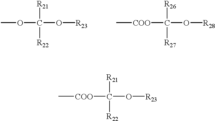
- R 18 , R 19 , R 21 , and R 22 may or may not be the same as one another, and is each an alkyl group having 1 to 4 carbon atoms which may have a hydrogen atom or a halogen atom as a substituent.
- R 20 is an alkyl group having 1 to 4 carbon atoms which may have a silyl group, an oxysilyl group, or a halogen atom as a substituent.
- R 23 is an alkyl group, cycloalkyl group, aralkyl group, alkenyl group, aryloxyalkyl group, aralkyloxyalkyl group, or cycloalkyl-alkyl group which may have a hydroxyl group, halogen atom, acyl group, or a substituent.
- R 17 denotes either of the following groups.
- R 26 and R 27 are each synonymous to the above R 18 , R 19 , R 21 , and R 22 .
- R 28 is an alkyl group, cycloalkyl group, aryl group, or aralkyl group which may have a substituent.
- R 26 and R 27 and/or R 28 may be bonded to one another to form a single ring or multiple ring having 4 to 9 members.
- R 29 is an alkyl group, cycloalkyl group, aryl group, aralkyl group, alkoxy group, acyl group, acylamino group, or alkoxycarbonyl group which may have a hydrogen atom, halogen atom, or a substituent.
- R 12 is an alkyl group, aralkyl group, or alkoxy group which may have a hydrogen atom, halogen atom, or a substituent, or a group expressed by —COZR 13 (Z and R 13 are synonymous to the above Z and R 13 ), or either of the following substituents.
- Z and R 15 are synonymous to the above Z and R 15 .
- R 24 is synonymous to the above R 29 .
- a, c, and d are each 0 or a positive integer, and b is a positive integer.
- e is 0 or an integer of 1 to 4; f and g are each an integer of 1 to 4; and h is an integer of 1 to 6.
- Ra, Rb, and Rc each denote a hydrocarbon group which may have a hydrogen atom, or a substituent, independently of each other. s denotes an integer of 2 or greater.
- R 1 to R 3 and R 5 to R 7 may or may not be the same as one another, and are each an alkyl group, aralkyl group, or alkoxy group which may have a hydrogen atom, halogen atom, a group expressed by —C( ⁇ O)—Z—R 13 , or a substituent.
- Z denotes a single bond, —O—, —NH—, or —N(R 25 )—.
- R 13 and R 25 may or may not be the same as one another, and each denote an alkyl group, cycloalkyl group, or aralkyl group which may have a substituent.
- R 4 and R 8 may or may not be the same as one another, and each denote a group having a valence of 2 to 5 which is expressed by the following formula.
- a 1 to A 5 may or may not be the same as one another, and each denote a hydrogen atom, —R 14 or a single bond, and at least one of the A 1 to A 5 denotes a single bond.
- R 15 is a single bond or a group expressed by —R 30 —Y 3 —.
- Z denotes a single bond or a group expressed by —O—, —NH—, or —NR 25 —.
- R 14 is synonymous to R 1 to R 3 and R 5 to R 7 .
- R 30 is an alkylene group or cycloalkylene group which may have a substituent.
- Y 3 is a single bond, —S—, —O—, or —OC( ⁇ O)—.
- R 25 is synonymous to the above R 25 .
- R 2 and R 4 or R 6 and R 8 may be bonded to each other to form the following group.
- Y 0 is defined in the same manner as R 4 and R 8 , and Y 0 is bonded to G or Q.
- G denotes a group selected from the group of chemical groups comprising —OH, —COOH, —CONHCOR 16 , —CONHSO 2 —R 16 , and —SO 2 NH—R 16 .
- R 16 is an alkyl group, cycloalkyl group, acyl group, or aryl group which may have a substituent.
- R 21 , and R 22 may or may not be the same as one another, and is each an alkyl group having 1 to 4 carbon atoms which may have a hydrogen atom or a halogen atom as a substituent.
- R 23 is an alkyl group, cycloalkyl group, aryl group, or aralkyl group which may have a substituent.
- the R 26 and R 27 may or may not be the same as one another, and are each synonymous to the R 21 and R 22 .
- R 28 is an alkyl group, cycloalkyl group, aryl group, or aralkyl group which may have a substituent.
- a is an integer of 0 or greater, and b is a positive integer.
- f and g are each an integer of 1 to 4.
- the compound which has a group capable of being crosslinked by an acid will be described.
- a compound produced by causing formaldehyde to act upon melamine, benzoguanamine, glycoluryl, or the like, or its alkyl modified substance, an epoxy compound, aldehydes, an azide compound, an organic peroxide, hexamethylenetetramine, and the like can be mentioned. partially reacted products of these and aqueous-alkali-soluble plastics can be effectively used.
- the compounds for use in the embodiments of the present invention which have an olefin unsaturated group preferably have a boiling point of 100° C. or over under the normal pressure.
Landscapes
- Physics & Mathematics (AREA)
- General Physics & Mathematics (AREA)
- Spectroscopy & Molecular Physics (AREA)
- Engineering & Computer Science (AREA)
- Architecture (AREA)
- Structural Engineering (AREA)
- Materials For Photolithography (AREA)
- Drying Of Semiconductors (AREA)
- Photosensitive Polymer And Photoresist Processing (AREA)
- Exposure Of Semiconductors, Excluding Electron Or Ion Beam Exposure (AREA)
Abstract
Description


Claims (18)
Applications Claiming Priority (2)
| Application Number | Priority Date | Filing Date | Title |
|---|---|---|---|
| JP12338999 | 1999-04-30 | ||
| JP11-123389 | 1999-04-30 |
Publications (1)
| Publication Number | Publication Date |
|---|---|
| US6497996B1 true US6497996B1 (en) | 2002-12-24 |
Family
ID=14859373
Family Applications (1)
| Application Number | Title | Priority Date | Filing Date |
|---|---|---|---|
| US09/562,076 Expired - Fee Related US6497996B1 (en) | 1999-04-30 | 2000-05-01 | Fine pattern forming method |
Country Status (2)
| Country | Link |
|---|---|
| US (1) | US6497996B1 (en) |
| EP (1) | EP1054296A3 (en) |
Cited By (13)
| Publication number | Priority date | Publication date | Assignee | Title |
|---|---|---|---|---|
| US20030025319A1 (en) * | 2001-08-02 | 2003-02-06 | Eastman Kodak Company | Authentication using near-field optical imaging |
| US6566280B1 (en) * | 2002-08-26 | 2003-05-20 | Intel Corporation | Forming polymer features on a substrate |
| US6707538B2 (en) * | 2001-06-21 | 2004-03-16 | Fuji Photo Film Co., Ltd. | Near-field exposure system selectively applying linearly polarized exposure light to exposure mask |
| US20040131976A1 (en) * | 2003-01-03 | 2004-07-08 | Chu-Wei Hsu | Method of forming a thin film transistor liquid crystal display |
| US6849391B2 (en) * | 2001-06-12 | 2005-02-01 | Canon Kabushiki Kaisha | Photoresist, photolithography method using the same, and method for producing photoresist |
| US20050064301A1 (en) * | 2003-09-08 | 2005-03-24 | Canon Kabushiki Kaisha | Mask manufacturing method |
| US20050233255A1 (en) * | 2000-09-27 | 2005-10-20 | Kabushiki Kaisha Toshiba | Method for forming pattern |
| US20060003236A1 (en) * | 2004-06-30 | 2006-01-05 | Canon Kabushiki Kaisha | Photomask and near-field exposure method |
| US20060003233A1 (en) * | 2003-06-26 | 2006-01-05 | Cannon Kabushiki Kaisha | Exposure mask, method of designing and manufacturing the same, exposure method and apparatus, pattern forming method, and device manufacturing method |
| US6998223B1 (en) * | 1999-08-27 | 2006-02-14 | Fuji Photo Film Co., Ltd. | Optical wavelength converting device and process for producing the same |
| US20060240639A1 (en) * | 2005-03-31 | 2006-10-26 | Kazutaka Akiyama | Fine patterning method for semiconductor device |
| US20080179281A1 (en) * | 2007-01-31 | 2008-07-31 | Advanced Micro Devices, Inc. | Methods for fabricating device features having small dimensions |
| WO2014159427A1 (en) * | 2013-03-14 | 2014-10-02 | Applied Materials, Inc | Resist hardening and development processes for semiconductor device manufacturing |
Families Citing this family (1)
| Publication number | Priority date | Publication date | Assignee | Title |
|---|---|---|---|---|
| JP4261849B2 (en) * | 2002-09-06 | 2009-04-30 | キヤノン株式会社 | Exposure method using near-field light and exposure apparatus using near-field light |
Citations (10)
| Publication number | Priority date | Publication date | Assignee | Title |
|---|---|---|---|---|
| EP0229629A2 (en) | 1986-01-08 | 1987-07-22 | Hitachi, Ltd. | Photosensitive resin composition |
| US4737425A (en) * | 1986-06-10 | 1988-04-12 | International Business Machines Corporation | Patterned resist and process |
| US4782008A (en) * | 1985-03-19 | 1988-11-01 | International Business Machines Corporation | Plasma-resistant polymeric material, preparation thereof, and use thereof |
| US4822716A (en) | 1985-12-27 | 1989-04-18 | Kabushiki Kaisha Toshiba | Polysilanes, Polysiloxanes and silicone resist materials containing these compounds |
| EP0330209A2 (en) | 1988-02-26 | 1989-08-30 | BASF Aktiengesellschaft | Photoreactive polymers and process for the production of a two-layer resist |
| US4931351A (en) * | 1987-01-12 | 1990-06-05 | Eastman Kodak Company | Bilayer lithographic process |
| US5234793A (en) * | 1989-04-24 | 1993-08-10 | Siemens Aktiengesellschaft | Method for dimensionally accurate structure transfer in bilayer technique wherein a treating step with a bulging agent is employed after development |
| US5512334A (en) | 1991-09-27 | 1996-04-30 | Siemens Aktiengesellschaft | Method for the production of a bottom resist |
| US5532105A (en) | 1992-08-07 | 1996-07-02 | Hitachi Chemical Company, Ltd. | Photolithographically viahole-forming photosensitive element comprising two photosensitive layers for the fabrication process of multilayer wiring board |
| JPH11317345A (en) | 1998-04-30 | 1999-11-16 | Ebara Corp | Transfer/working method for minute pattern |
Family Cites Families (1)
| Publication number | Priority date | Publication date | Assignee | Title |
|---|---|---|---|---|
| JP2793251B2 (en) * | 1989-05-09 | 1998-09-03 | 株式会社東芝 | Pattern formation method |
-
2000
- 2000-04-28 EP EP00109254A patent/EP1054296A3/en not_active Ceased
- 2000-05-01 US US09/562,076 patent/US6497996B1/en not_active Expired - Fee Related
Patent Citations (10)
| Publication number | Priority date | Publication date | Assignee | Title |
|---|---|---|---|---|
| US4782008A (en) * | 1985-03-19 | 1988-11-01 | International Business Machines Corporation | Plasma-resistant polymeric material, preparation thereof, and use thereof |
| US4822716A (en) | 1985-12-27 | 1989-04-18 | Kabushiki Kaisha Toshiba | Polysilanes, Polysiloxanes and silicone resist materials containing these compounds |
| EP0229629A2 (en) | 1986-01-08 | 1987-07-22 | Hitachi, Ltd. | Photosensitive resin composition |
| US4737425A (en) * | 1986-06-10 | 1988-04-12 | International Business Machines Corporation | Patterned resist and process |
| US4931351A (en) * | 1987-01-12 | 1990-06-05 | Eastman Kodak Company | Bilayer lithographic process |
| EP0330209A2 (en) | 1988-02-26 | 1989-08-30 | BASF Aktiengesellschaft | Photoreactive polymers and process for the production of a two-layer resist |
| US5234793A (en) * | 1989-04-24 | 1993-08-10 | Siemens Aktiengesellschaft | Method for dimensionally accurate structure transfer in bilayer technique wherein a treating step with a bulging agent is employed after development |
| US5512334A (en) | 1991-09-27 | 1996-04-30 | Siemens Aktiengesellschaft | Method for the production of a bottom resist |
| US5532105A (en) | 1992-08-07 | 1996-07-02 | Hitachi Chemical Company, Ltd. | Photolithographically viahole-forming photosensitive element comprising two photosensitive layers for the fabrication process of multilayer wiring board |
| JPH11317345A (en) | 1998-04-30 | 1999-11-16 | Ebara Corp | Transfer/working method for minute pattern |
Non-Patent Citations (1)
| Title |
|---|
| Patent Abstracts of Japan vol. 015, No. 071 (P-1168), Feb. 19, 1991 (Abstract of JP 02 293850, Dec. 5, 1990). |
Cited By (24)
| Publication number | Priority date | Publication date | Assignee | Title |
|---|---|---|---|---|
| US6998223B1 (en) * | 1999-08-27 | 2006-02-14 | Fuji Photo Film Co., Ltd. | Optical wavelength converting device and process for producing the same |
| US7177072B2 (en) | 1999-08-27 | 2007-02-13 | Fuji Photo Film Co., Ltd. | Optical wavelength converting device and process for producing the same |
| US20060099533A1 (en) * | 1999-08-27 | 2006-05-11 | Fuji Photo Film Co., Ltd. | Optical wavelength converting device and process for producing the same |
| US7198886B2 (en) | 2000-09-27 | 2007-04-03 | Kabushiki Kaisha Toshiba | Method for forming pattern |
| US20050233255A1 (en) * | 2000-09-27 | 2005-10-20 | Kabushiki Kaisha Toshiba | Method for forming pattern |
| US7303859B2 (en) | 2001-06-12 | 2007-12-04 | Canon Kabushiki Kaisha | Photoresist, photolithography method using the same, and method for producing photoresist |
| US6849391B2 (en) * | 2001-06-12 | 2005-02-01 | Canon Kabushiki Kaisha | Photoresist, photolithography method using the same, and method for producing photoresist |
| US20050053859A1 (en) * | 2001-06-12 | 2005-03-10 | Canon Kabushiki Kaisha | Photoresist, photolithography method using the same, and method for producing photoresist |
| US20060263722A1 (en) * | 2001-06-12 | 2006-11-23 | Canon Kabushiki Kaisha | Photoresist, photolithography method using the same, and method for producing photoresist |
| US6707538B2 (en) * | 2001-06-21 | 2004-03-16 | Fuji Photo Film Co., Ltd. | Near-field exposure system selectively applying linearly polarized exposure light to exposure mask |
| US20030025319A1 (en) * | 2001-08-02 | 2003-02-06 | Eastman Kodak Company | Authentication using near-field optical imaging |
| US8403367B2 (en) * | 2001-08-02 | 2013-03-26 | Eastman Kodak Company | Authentication using near-field optical imaging |
| US6566280B1 (en) * | 2002-08-26 | 2003-05-20 | Intel Corporation | Forming polymer features on a substrate |
| US20040131976A1 (en) * | 2003-01-03 | 2004-07-08 | Chu-Wei Hsu | Method of forming a thin film transistor liquid crystal display |
| US20060003233A1 (en) * | 2003-06-26 | 2006-01-05 | Cannon Kabushiki Kaisha | Exposure mask, method of designing and manufacturing the same, exposure method and apparatus, pattern forming method, and device manufacturing method |
| US7691540B2 (en) | 2003-06-26 | 2010-04-06 | Canon Kabushiki Kaisha | Exposure mask, method of designing and manufacturing the same, exposure method and apparatus, pattern forming method, and device manufacturing method |
| US20050064301A1 (en) * | 2003-09-08 | 2005-03-24 | Canon Kabushiki Kaisha | Mask manufacturing method |
| US20060003236A1 (en) * | 2004-06-30 | 2006-01-05 | Canon Kabushiki Kaisha | Photomask and near-field exposure method |
| US20060240639A1 (en) * | 2005-03-31 | 2006-10-26 | Kazutaka Akiyama | Fine patterning method for semiconductor device |
| US7611994B2 (en) | 2005-03-31 | 2009-11-03 | Kabushiki Kaisha Toshiba | Fine patterning method for semiconductor device |
| US7601645B2 (en) * | 2007-01-31 | 2009-10-13 | Globalfoundries Inc. | Methods for fabricating device features having small dimensions |
| US20080179281A1 (en) * | 2007-01-31 | 2008-07-31 | Advanced Micro Devices, Inc. | Methods for fabricating device features having small dimensions |
| WO2014159427A1 (en) * | 2013-03-14 | 2014-10-02 | Applied Materials, Inc | Resist hardening and development processes for semiconductor device manufacturing |
| US9411237B2 (en) | 2013-03-14 | 2016-08-09 | Applied Materials, Inc. | Resist hardening and development processes for semiconductor device manufacturing |
Also Published As
| Publication number | Publication date |
|---|---|
| EP1054296A2 (en) | 2000-11-22 |
| EP1054296A3 (en) | 2002-03-06 |
Similar Documents
| Publication | Publication Date | Title |
|---|---|---|
| US6497996B1 (en) | Fine pattern forming method | |
| JP4086830B2 (en) | Silicon-containing composition for spin-on ARC / hard mask | |
| TWI247975B (en) | Modification of 193 nm sensitive photoresist materials by electron beam exposure | |
| US8034546B2 (en) | Use of methanofullerne derivatives as resist materials and method for forming a resist layer | |
| JP2501292B2 (en) | Method for making acid sensitive polymers and photoresist structures | |
| US7326442B2 (en) | Antireflective composition and process of making a lithographic structure | |
| US6753129B2 (en) | Method and apparatus for modification of chemically amplified photoresist by electron beam exposure | |
| US6900001B2 (en) | Method for modifying resist images by electron beam exposure | |
| JP2005070776A (en) | Antireflective hardmask composition and method for manufacturing semiconductor device using same | |
| JPH11258814A (en) | Antireflection coating composition having high conformality | |
| JP2001021710A (en) | Manufacture for diffraction grating | |
| US20050106494A1 (en) | Silicon-containing resist systems with cyclic ketal protecting groups | |
| JPH09235326A (en) | Acetal group-containing alkoxy-styrene polymer, its production and chemical amplification type photoresist material comprising alkoxy-styrene polymer as main component | |
| US6821718B2 (en) | Radiation sensitive silicon-containing negative resists and use thereof | |
| US6835532B2 (en) | Organic anti-reflective coating composition and method for forming photoresist patterns using the same | |
| US6673525B1 (en) | Thin layer imaging process for microlithography using radiation at strongly attenuated wavelengths | |
| JP2001015427A (en) | Formation of fine pattern | |
| JPH10507588A (en) | Method of treating anti-reflective coating on substrate | |
| JP2001015426A (en) | Formation of fine pattern | |
| JP2667742B2 (en) | Photosensitive resin composition | |
| TWI273349B (en) | A low outgassing and non-crosslinking series of polymers for EUV negative tone photoresists | |
| US7670749B2 (en) | Resist material and method for forming a patterned resist layer on a substrate | |
| JP2648004B2 (en) | Etching resistant pattern forming method | |
| EP0396254A2 (en) | Photosensitive composition and pattern formation method using the same | |
| JPH0290169A (en) | Pattern forming method |
Legal Events
| Date | Code | Title | Description |
|---|---|---|---|
| AS | Assignment |
Owner name: FUJI PHOTO FILM CO., LTD., JAPAN Free format text: ASSIGNMENT OF ASSIGNORS INTEREST;ASSIGNORS:NAYA, MASAYUKI;SAKAGUCHI, SHINJI;REEL/FRAME:011107/0988 Effective date: 20000523 |
|
| FEPP | Fee payment procedure |
Free format text: PAYOR NUMBER ASSIGNED (ORIGINAL EVENT CODE: ASPN); ENTITY STATUS OF PATENT OWNER: LARGE ENTITY |
|
| FPAY | Fee payment |
Year of fee payment: 4 |
|
| AS | Assignment |
Owner name: FUJIFILM CORPORATION, JAPAN Free format text: ASSIGNMENT OF ASSIGNORS INTEREST;ASSIGNOR:FUJIFILM HOLDINGS CORPORATION (FORMERLY FUJI PHOTO FILM CO., LTD.);REEL/FRAME:018904/0001 Effective date: 20070130 Owner name: FUJIFILM CORPORATION,JAPAN Free format text: ASSIGNMENT OF ASSIGNORS INTEREST;ASSIGNOR:FUJIFILM HOLDINGS CORPORATION (FORMERLY FUJI PHOTO FILM CO., LTD.);REEL/FRAME:018904/0001 Effective date: 20070130 |
|
| FPAY | Fee payment |
Year of fee payment: 8 |
|
| REMI | Maintenance fee reminder mailed | ||
| LAPS | Lapse for failure to pay maintenance fees | ||
| STCH | Information on status: patent discontinuation |
Free format text: PATENT EXPIRED DUE TO NONPAYMENT OF MAINTENANCE FEES UNDER 37 CFR 1.362 |
|
| FP | Lapsed due to failure to pay maintenance fee |
Effective date: 20141224 |