US6503343B1 - Controlled plating on reactive metals - Google Patents
Controlled plating on reactive metals Download PDFInfo
- Publication number
- US6503343B1 US6503343B1 US09/658,643 US65864300A US6503343B1 US 6503343 B1 US6503343 B1 US 6503343B1 US 65864300 A US65864300 A US 65864300A US 6503343 B1 US6503343 B1 US 6503343B1
- Authority
- US
- United States
- Prior art keywords
- metal
- solution
- deposited
- surface oxide
- ions
- Prior art date
- Legal status (The legal status is an assumption and is not a legal conclusion. Google has not performed a legal analysis and makes no representation as to the accuracy of the status listed.)
- Expired - Lifetime
Links
Images


Classifications
-
- H—ELECTRICITY
- H01—ELECTRIC ELEMENTS
- H01L—SEMICONDUCTOR DEVICES NOT COVERED BY CLASS H10
- H01L21/00—Processes or apparatus adapted for the manufacture or treatment of semiconductor or solid state devices or of parts thereof
- H01L21/02—Manufacture or treatment of semiconductor devices or of parts thereof
- H01L21/04—Manufacture or treatment of semiconductor devices or of parts thereof the devices having at least one potential-jump barrier or surface barrier, e.g. PN junction, depletion layer or carrier concentration layer
- H01L21/18—Manufacture or treatment of semiconductor devices or of parts thereof the devices having at least one potential-jump barrier or surface barrier, e.g. PN junction, depletion layer or carrier concentration layer the devices having semiconductor bodies comprising elements of Group IV of the Periodic System or AIIIBV compounds with or without impurities, e.g. doping materials
- H01L21/28—Manufacture of electrodes on semiconductor bodies using processes or apparatus not provided for in groups H01L21/20 - H01L21/268
- H01L21/283—Deposition of conductive or insulating materials for electrodes conducting electric current
- H01L21/288—Deposition of conductive or insulating materials for electrodes conducting electric current from a liquid, e.g. electrolytic deposition
-
- C—CHEMISTRY; METALLURGY
- C23—COATING METALLIC MATERIAL; COATING MATERIAL WITH METALLIC MATERIAL; CHEMICAL SURFACE TREATMENT; DIFFUSION TREATMENT OF METALLIC MATERIAL; COATING BY VACUUM EVAPORATION, BY SPUTTERING, BY ION IMPLANTATION OR BY CHEMICAL VAPOUR DEPOSITION, IN GENERAL; INHIBITING CORROSION OF METALLIC MATERIAL OR INCRUSTATION IN GENERAL
- C23C—COATING METALLIC MATERIAL; COATING MATERIAL WITH METALLIC MATERIAL; SURFACE TREATMENT OF METALLIC MATERIAL BY DIFFUSION INTO THE SURFACE, BY CHEMICAL CONVERSION OR SUBSTITUTION; COATING BY VACUUM EVAPORATION, BY SPUTTERING, BY ION IMPLANTATION OR BY CHEMICAL VAPOUR DEPOSITION, IN GENERAL
- C23C18/00—Chemical coating by decomposition of either liquid compounds or solutions of the coating forming compounds, without leaving reaction products of surface material in the coating; Contact plating
- C23C18/16—Chemical coating by decomposition of either liquid compounds or solutions of the coating forming compounds, without leaving reaction products of surface material in the coating; Contact plating by reduction or substitution, e.g. electroless plating
- C23C18/1601—Process or apparatus
- C23C18/1633—Process of electroless plating
- C23C18/1646—Characteristics of the product obtained
- C23C18/165—Multilayered product
- C23C18/1651—Two or more layers only obtained by electroless plating
-
- C—CHEMISTRY; METALLURGY
- C23—COATING METALLIC MATERIAL; COATING MATERIAL WITH METALLIC MATERIAL; CHEMICAL SURFACE TREATMENT; DIFFUSION TREATMENT OF METALLIC MATERIAL; COATING BY VACUUM EVAPORATION, BY SPUTTERING, BY ION IMPLANTATION OR BY CHEMICAL VAPOUR DEPOSITION, IN GENERAL; INHIBITING CORROSION OF METALLIC MATERIAL OR INCRUSTATION IN GENERAL
- C23C—COATING METALLIC MATERIAL; COATING MATERIAL WITH METALLIC MATERIAL; SURFACE TREATMENT OF METALLIC MATERIAL BY DIFFUSION INTO THE SURFACE, BY CHEMICAL CONVERSION OR SUBSTITUTION; COATING BY VACUUM EVAPORATION, BY SPUTTERING, BY ION IMPLANTATION OR BY CHEMICAL VAPOUR DEPOSITION, IN GENERAL
- C23C18/00—Chemical coating by decomposition of either liquid compounds or solutions of the coating forming compounds, without leaving reaction products of surface material in the coating; Contact plating
- C23C18/16—Chemical coating by decomposition of either liquid compounds or solutions of the coating forming compounds, without leaving reaction products of surface material in the coating; Contact plating by reduction or substitution, e.g. electroless plating
- C23C18/1601—Process or apparatus
- C23C18/1633—Process of electroless plating
- C23C18/1646—Characteristics of the product obtained
- C23C18/165—Multilayered product
- C23C18/1653—Two or more layers with at least one layer obtained by electroless plating and one layer obtained by electroplating
-
- C—CHEMISTRY; METALLURGY
- C23—COATING METALLIC MATERIAL; COATING MATERIAL WITH METALLIC MATERIAL; CHEMICAL SURFACE TREATMENT; DIFFUSION TREATMENT OF METALLIC MATERIAL; COATING BY VACUUM EVAPORATION, BY SPUTTERING, BY ION IMPLANTATION OR BY CHEMICAL VAPOUR DEPOSITION, IN GENERAL; INHIBITING CORROSION OF METALLIC MATERIAL OR INCRUSTATION IN GENERAL
- C23C—COATING METALLIC MATERIAL; COATING MATERIAL WITH METALLIC MATERIAL; SURFACE TREATMENT OF METALLIC MATERIAL BY DIFFUSION INTO THE SURFACE, BY CHEMICAL CONVERSION OR SUBSTITUTION; COATING BY VACUUM EVAPORATION, BY SPUTTERING, BY ION IMPLANTATION OR BY CHEMICAL VAPOUR DEPOSITION, IN GENERAL
- C23C18/00—Chemical coating by decomposition of either liquid compounds or solutions of the coating forming compounds, without leaving reaction products of surface material in the coating; Contact plating
- C23C18/16—Chemical coating by decomposition of either liquid compounds or solutions of the coating forming compounds, without leaving reaction products of surface material in the coating; Contact plating by reduction or substitution, e.g. electroless plating
- C23C18/31—Coating with metals
- C23C18/32—Coating with nickel, cobalt or mixtures thereof with phosphorus or boron
-
- C—CHEMISTRY; METALLURGY
- C23—COATING METALLIC MATERIAL; COATING MATERIAL WITH METALLIC MATERIAL; CHEMICAL SURFACE TREATMENT; DIFFUSION TREATMENT OF METALLIC MATERIAL; COATING BY VACUUM EVAPORATION, BY SPUTTERING, BY ION IMPLANTATION OR BY CHEMICAL VAPOUR DEPOSITION, IN GENERAL; INHIBITING CORROSION OF METALLIC MATERIAL OR INCRUSTATION IN GENERAL
- C23C—COATING METALLIC MATERIAL; COATING MATERIAL WITH METALLIC MATERIAL; SURFACE TREATMENT OF METALLIC MATERIAL BY DIFFUSION INTO THE SURFACE, BY CHEMICAL CONVERSION OR SUBSTITUTION; COATING BY VACUUM EVAPORATION, BY SPUTTERING, BY ION IMPLANTATION OR BY CHEMICAL VAPOUR DEPOSITION, IN GENERAL
- C23C18/00—Chemical coating by decomposition of either liquid compounds or solutions of the coating forming compounds, without leaving reaction products of surface material in the coating; Contact plating
- C23C18/16—Chemical coating by decomposition of either liquid compounds or solutions of the coating forming compounds, without leaving reaction products of surface material in the coating; Contact plating by reduction or substitution, e.g. electroless plating
- C23C18/31—Coating with metals
- C23C18/42—Coating with noble metals
-
- C—CHEMISTRY; METALLURGY
- C23—COATING METALLIC MATERIAL; COATING MATERIAL WITH METALLIC MATERIAL; CHEMICAL SURFACE TREATMENT; DIFFUSION TREATMENT OF METALLIC MATERIAL; COATING BY VACUUM EVAPORATION, BY SPUTTERING, BY ION IMPLANTATION OR BY CHEMICAL VAPOUR DEPOSITION, IN GENERAL; INHIBITING CORROSION OF METALLIC MATERIAL OR INCRUSTATION IN GENERAL
- C23C—COATING METALLIC MATERIAL; COATING MATERIAL WITH METALLIC MATERIAL; SURFACE TREATMENT OF METALLIC MATERIAL BY DIFFUSION INTO THE SURFACE, BY CHEMICAL CONVERSION OR SUBSTITUTION; COATING BY VACUUM EVAPORATION, BY SPUTTERING, BY ION IMPLANTATION OR BY CHEMICAL VAPOUR DEPOSITION, IN GENERAL
- C23C18/00—Chemical coating by decomposition of either liquid compounds or solutions of the coating forming compounds, without leaving reaction products of surface material in the coating; Contact plating
- C23C18/54—Contact plating, i.e. electroless electrochemical plating
-
- H—ELECTRICITY
- H01—ELECTRIC ELEMENTS
- H01L—SEMICONDUCTOR DEVICES NOT COVERED BY CLASS H10
- H01L24/00—Arrangements for connecting or disconnecting semiconductor or solid-state bodies; Methods or apparatus related thereto
- H01L24/01—Means for bonding being attached to, or being formed on, the surface to be connected, e.g. chip-to-package, die-attach, "first-level" interconnects; Manufacturing methods related thereto
- H01L24/10—Bump connectors ; Manufacturing methods related thereto
- H01L24/11—Manufacturing methods
-
- H—ELECTRICITY
- H01—ELECTRIC ELEMENTS
- H01L—SEMICONDUCTOR DEVICES NOT COVERED BY CLASS H10
- H01L2224/00—Indexing scheme for arrangements for connecting or disconnecting semiconductor or solid-state bodies and methods related thereto as covered by H01L24/00
- H01L2224/01—Means for bonding being attached to, or being formed on, the surface to be connected, e.g. chip-to-package, die-attach, "first-level" interconnects; Manufacturing methods related thereto
- H01L2224/10—Bump connectors; Manufacturing methods related thereto
- H01L2224/12—Structure, shape, material or disposition of the bump connectors prior to the connecting process
- H01L2224/13—Structure, shape, material or disposition of the bump connectors prior to the connecting process of an individual bump connector
- H01L2224/13001—Core members of the bump connector
- H01L2224/13099—Material
-
- H—ELECTRICITY
- H01—ELECTRIC ELEMENTS
- H01L—SEMICONDUCTOR DEVICES NOT COVERED BY CLASS H10
- H01L2224/00—Indexing scheme for arrangements for connecting or disconnecting semiconductor or solid-state bodies and methods related thereto as covered by H01L24/00
- H01L2224/01—Means for bonding being attached to, or being formed on, the surface to be connected, e.g. chip-to-package, die-attach, "first-level" interconnects; Manufacturing methods related thereto
- H01L2224/42—Wire connectors; Manufacturing methods related thereto
- H01L2224/44—Structure, shape, material or disposition of the wire connectors prior to the connecting process
- H01L2224/45—Structure, shape, material or disposition of the wire connectors prior to the connecting process of an individual wire connector
- H01L2224/45001—Core members of the connector
- H01L2224/45099—Material
- H01L2224/451—Material with a principal constituent of the material being a metal or a metalloid, e.g. boron (B), silicon (Si), germanium (Ge), arsenic (As), antimony (Sb), tellurium (Te) and polonium (Po), and alloys thereof
- H01L2224/45138—Material with a principal constituent of the material being a metal or a metalloid, e.g. boron (B), silicon (Si), germanium (Ge), arsenic (As), antimony (Sb), tellurium (Te) and polonium (Po), and alloys thereof the principal constituent melting at a temperature of greater than or equal to 950°C and less than 1550°C
- H01L2224/45144—Gold (Au) as principal constituent
-
- H—ELECTRICITY
- H01—ELECTRIC ELEMENTS
- H01L—SEMICONDUCTOR DEVICES NOT COVERED BY CLASS H10
- H01L2924/00—Indexing scheme for arrangements or methods for connecting or disconnecting semiconductor or solid-state bodies as covered by H01L24/00
- H01L2924/01—Chemical elements
- H01L2924/01004—Beryllium [Be]
-
- H—ELECTRICITY
- H01—ELECTRIC ELEMENTS
- H01L—SEMICONDUCTOR DEVICES NOT COVERED BY CLASS H10
- H01L2924/00—Indexing scheme for arrangements or methods for connecting or disconnecting semiconductor or solid-state bodies as covered by H01L24/00
- H01L2924/01—Chemical elements
- H01L2924/01005—Boron [B]
-
- H—ELECTRICITY
- H01—ELECTRIC ELEMENTS
- H01L—SEMICONDUCTOR DEVICES NOT COVERED BY CLASS H10
- H01L2924/00—Indexing scheme for arrangements or methods for connecting or disconnecting semiconductor or solid-state bodies as covered by H01L24/00
- H01L2924/01—Chemical elements
- H01L2924/01006—Carbon [C]
-
- H—ELECTRICITY
- H01—ELECTRIC ELEMENTS
- H01L—SEMICONDUCTOR DEVICES NOT COVERED BY CLASS H10
- H01L2924/00—Indexing scheme for arrangements or methods for connecting or disconnecting semiconductor or solid-state bodies as covered by H01L24/00
- H01L2924/01—Chemical elements
- H01L2924/01012—Magnesium [Mg]
-
- H—ELECTRICITY
- H01—ELECTRIC ELEMENTS
- H01L—SEMICONDUCTOR DEVICES NOT COVERED BY CLASS H10
- H01L2924/00—Indexing scheme for arrangements or methods for connecting or disconnecting semiconductor or solid-state bodies as covered by H01L24/00
- H01L2924/01—Chemical elements
- H01L2924/01013—Aluminum [Al]
-
- H—ELECTRICITY
- H01—ELECTRIC ELEMENTS
- H01L—SEMICONDUCTOR DEVICES NOT COVERED BY CLASS H10
- H01L2924/00—Indexing scheme for arrangements or methods for connecting or disconnecting semiconductor or solid-state bodies as covered by H01L24/00
- H01L2924/01—Chemical elements
- H01L2924/01015—Phosphorus [P]
-
- H—ELECTRICITY
- H01—ELECTRIC ELEMENTS
- H01L—SEMICONDUCTOR DEVICES NOT COVERED BY CLASS H10
- H01L2924/00—Indexing scheme for arrangements or methods for connecting or disconnecting semiconductor or solid-state bodies as covered by H01L24/00
- H01L2924/01—Chemical elements
- H01L2924/01016—Sulfur [S]
-
- H—ELECTRICITY
- H01—ELECTRIC ELEMENTS
- H01L—SEMICONDUCTOR DEVICES NOT COVERED BY CLASS H10
- H01L2924/00—Indexing scheme for arrangements or methods for connecting or disconnecting semiconductor or solid-state bodies as covered by H01L24/00
- H01L2924/01—Chemical elements
- H01L2924/01022—Titanium [Ti]
-
- H—ELECTRICITY
- H01—ELECTRIC ELEMENTS
- H01L—SEMICONDUCTOR DEVICES NOT COVERED BY CLASS H10
- H01L2924/00—Indexing scheme for arrangements or methods for connecting or disconnecting semiconductor or solid-state bodies as covered by H01L24/00
- H01L2924/01—Chemical elements
- H01L2924/01027—Cobalt [Co]
-
- H—ELECTRICITY
- H01—ELECTRIC ELEMENTS
- H01L—SEMICONDUCTOR DEVICES NOT COVERED BY CLASS H10
- H01L2924/00—Indexing scheme for arrangements or methods for connecting or disconnecting semiconductor or solid-state bodies as covered by H01L24/00
- H01L2924/01—Chemical elements
- H01L2924/01029—Copper [Cu]
-
- H—ELECTRICITY
- H01—ELECTRIC ELEMENTS
- H01L—SEMICONDUCTOR DEVICES NOT COVERED BY CLASS H10
- H01L2924/00—Indexing scheme for arrangements or methods for connecting or disconnecting semiconductor or solid-state bodies as covered by H01L24/00
- H01L2924/01—Chemical elements
- H01L2924/0103—Zinc [Zn]
-
- H—ELECTRICITY
- H01—ELECTRIC ELEMENTS
- H01L—SEMICONDUCTOR DEVICES NOT COVERED BY CLASS H10
- H01L2924/00—Indexing scheme for arrangements or methods for connecting or disconnecting semiconductor or solid-state bodies as covered by H01L24/00
- H01L2924/01—Chemical elements
- H01L2924/01033—Arsenic [As]
-
- H—ELECTRICITY
- H01—ELECTRIC ELEMENTS
- H01L—SEMICONDUCTOR DEVICES NOT COVERED BY CLASS H10
- H01L2924/00—Indexing scheme for arrangements or methods for connecting or disconnecting semiconductor or solid-state bodies as covered by H01L24/00
- H01L2924/01—Chemical elements
- H01L2924/01039—Yttrium [Y]
-
- H—ELECTRICITY
- H01—ELECTRIC ELEMENTS
- H01L—SEMICONDUCTOR DEVICES NOT COVERED BY CLASS H10
- H01L2924/00—Indexing scheme for arrangements or methods for connecting or disconnecting semiconductor or solid-state bodies as covered by H01L24/00
- H01L2924/01—Chemical elements
- H01L2924/01044—Ruthenium [Ru]
-
- H—ELECTRICITY
- H01—ELECTRIC ELEMENTS
- H01L—SEMICONDUCTOR DEVICES NOT COVERED BY CLASS H10
- H01L2924/00—Indexing scheme for arrangements or methods for connecting or disconnecting semiconductor or solid-state bodies as covered by H01L24/00
- H01L2924/01—Chemical elements
- H01L2924/01045—Rhodium [Rh]
-
- H—ELECTRICITY
- H01—ELECTRIC ELEMENTS
- H01L—SEMICONDUCTOR DEVICES NOT COVERED BY CLASS H10
- H01L2924/00—Indexing scheme for arrangements or methods for connecting or disconnecting semiconductor or solid-state bodies as covered by H01L24/00
- H01L2924/01—Chemical elements
- H01L2924/01046—Palladium [Pd]
-
- H—ELECTRICITY
- H01—ELECTRIC ELEMENTS
- H01L—SEMICONDUCTOR DEVICES NOT COVERED BY CLASS H10
- H01L2924/00—Indexing scheme for arrangements or methods for connecting or disconnecting semiconductor or solid-state bodies as covered by H01L24/00
- H01L2924/01—Chemical elements
- H01L2924/01072—Hafnium [Hf]
-
- H—ELECTRICITY
- H01—ELECTRIC ELEMENTS
- H01L—SEMICONDUCTOR DEVICES NOT COVERED BY CLASS H10
- H01L2924/00—Indexing scheme for arrangements or methods for connecting or disconnecting semiconductor or solid-state bodies as covered by H01L24/00
- H01L2924/01—Chemical elements
- H01L2924/01073—Tantalum [Ta]
-
- H—ELECTRICITY
- H01—ELECTRIC ELEMENTS
- H01L—SEMICONDUCTOR DEVICES NOT COVERED BY CLASS H10
- H01L2924/00—Indexing scheme for arrangements or methods for connecting or disconnecting semiconductor or solid-state bodies as covered by H01L24/00
- H01L2924/01—Chemical elements
- H01L2924/01074—Tungsten [W]
-
- H—ELECTRICITY
- H01—ELECTRIC ELEMENTS
- H01L—SEMICONDUCTOR DEVICES NOT COVERED BY CLASS H10
- H01L2924/00—Indexing scheme for arrangements or methods for connecting or disconnecting semiconductor or solid-state bodies as covered by H01L24/00
- H01L2924/01—Chemical elements
- H01L2924/01075—Rhenium [Re]
-
- H—ELECTRICITY
- H01—ELECTRIC ELEMENTS
- H01L—SEMICONDUCTOR DEVICES NOT COVERED BY CLASS H10
- H01L2924/00—Indexing scheme for arrangements or methods for connecting or disconnecting semiconductor or solid-state bodies as covered by H01L24/00
- H01L2924/01—Chemical elements
- H01L2924/01076—Osmium [Os]
-
- H—ELECTRICITY
- H01—ELECTRIC ELEMENTS
- H01L—SEMICONDUCTOR DEVICES NOT COVERED BY CLASS H10
- H01L2924/00—Indexing scheme for arrangements or methods for connecting or disconnecting semiconductor or solid-state bodies as covered by H01L24/00
- H01L2924/01—Chemical elements
- H01L2924/01077—Iridium [Ir]
-
- H—ELECTRICITY
- H01—ELECTRIC ELEMENTS
- H01L—SEMICONDUCTOR DEVICES NOT COVERED BY CLASS H10
- H01L2924/00—Indexing scheme for arrangements or methods for connecting or disconnecting semiconductor or solid-state bodies as covered by H01L24/00
- H01L2924/01—Chemical elements
- H01L2924/01078—Platinum [Pt]
-
- H—ELECTRICITY
- H01—ELECTRIC ELEMENTS
- H01L—SEMICONDUCTOR DEVICES NOT COVERED BY CLASS H10
- H01L2924/00—Indexing scheme for arrangements or methods for connecting or disconnecting semiconductor or solid-state bodies as covered by H01L24/00
- H01L2924/01—Chemical elements
- H01L2924/01079—Gold [Au]
-
- H—ELECTRICITY
- H01—ELECTRIC ELEMENTS
- H01L—SEMICONDUCTOR DEVICES NOT COVERED BY CLASS H10
- H01L2924/00—Indexing scheme for arrangements or methods for connecting or disconnecting semiconductor or solid-state bodies as covered by H01L24/00
- H01L2924/013—Alloys
- H01L2924/014—Solder alloys
-
- H—ELECTRICITY
- H01—ELECTRIC ELEMENTS
- H01L—SEMICONDUCTOR DEVICES NOT COVERED BY CLASS H10
- H01L2924/00—Indexing scheme for arrangements or methods for connecting or disconnecting semiconductor or solid-state bodies as covered by H01L24/00
- H01L2924/049—Nitrides composed of metals from groups of the periodic table
- H01L2924/0495—5th Group
- H01L2924/04953—TaN
-
- H—ELECTRICITY
- H01—ELECTRIC ELEMENTS
- H01L—SEMICONDUCTOR DEVICES NOT COVERED BY CLASS H10
- H01L2924/00—Indexing scheme for arrangements or methods for connecting or disconnecting semiconductor or solid-state bodies as covered by H01L24/00
- H01L2924/10—Details of semiconductor or other solid state devices to be connected
- H01L2924/102—Material of the semiconductor or solid state bodies
- H01L2924/1025—Semiconducting materials
- H01L2924/10251—Elemental semiconductors, i.e. Group IV
- H01L2924/10253—Silicon [Si]
-
- H—ELECTRICITY
- H01—ELECTRIC ELEMENTS
- H01L—SEMICONDUCTOR DEVICES NOT COVERED BY CLASS H10
- H01L2924/00—Indexing scheme for arrangements or methods for connecting or disconnecting semiconductor or solid-state bodies as covered by H01L24/00
- H01L2924/10—Details of semiconductor or other solid state devices to be connected
- H01L2924/11—Device type
- H01L2924/14—Integrated circuits
-
- H—ELECTRICITY
- H01—ELECTRIC ELEMENTS
- H01L—SEMICONDUCTOR DEVICES NOT COVERED BY CLASS H10
- H01L2924/00—Indexing scheme for arrangements or methods for connecting or disconnecting semiconductor or solid-state bodies as covered by H01L24/00
- H01L2924/30—Technical effects
- H01L2924/301—Electrical effects
- H01L2924/30107—Inductance
Definitions
- This invention is concerned with plating highly reactive metals, such as aluminum and its alloys, with more stable metals, such as nickel, that provide enhanced solderability, bondability and corrosion resistance.
- Aluminum is widely used for circuitry patterns on integrated circuit (IC) chips but is very difficult be directly solder because it is a very reactive metal that forms a thick oxide layer, which prevents direct contact between the solder and the aluminum metal.
- This thick oxide is recalcitrant in that it is difficult to remove and reforms almost instantaneously under ambient conditions. Consequently, electrical contact to aluminum IC pads is typically made by wire bonding, which utilizes a combination of ultrasonic vibration, pressure and thermal energy to cause a gold wire to penetrate the aluminum oxide layer and form a bond to the underlying metal.
- the other end of the gold wire is bonded to a pad on a substrate, or on a package (e.g., ball grid array or dual in-line package) that connects to a solderable pad or pin that is subsequently soldered to a printed wiring board (PWB) or other substrate.
- a package e.g., ball grid array or dual in-line package
- PWB printed wiring board
- Wire bonding imposes significant limitations for microelectronic applications. Since the bonds are made one at a time, the process is relatively slow and expensive compared to soldering, which can form thousands of connections almost simultaneously. The expense of the gold wire adds significantly to the costs. In addition, the fixture (head) for holding the gold wire and applying the pressure and energy needed for wire bonding has finite dimensions that limit the minimum spacing between adjacent bond sites. Another important drawback is the inductance of the gold wires themselves, which becomes appreciable at high signal frequencies and limits device switching times or clock speeds.
- solderable IC pads are essential to the emerging flip chip technology, which provides the ultimate in performance and cost reduction. In this case, pads on the IC chip are soldered directly to pads on the substrate PWB, which eliminates the cost and limitations of a package, provides area array capability, and minimizes signal losses.
- the thin metal buss layer needed to provide electrical contact to the aluminum pads is often deposited directly on the IC surface and must be removed by etching (after photoresist removal).
- a significant concern for electroplating processes is non-uniformity of the plated layers, especially overplating of isolated pads and underplating of those close together.
- Displacement plating from solution is attractive as a potential alternative for rendering aluminum pads solderable without the need for costly vacuum deposition, photoresist masking, and etching processes.
- the aluminum surface oxide would be dissolved in a solution that contains ions of a more noble metal, e.g., nickel, which would be deposited on the aluminum substrate by the electrons generated by aluminum dissolution in the solution. Since the displacement process should cease when the aluminum surface becomes completely covered with the displacement metal and is no longer exposed to the solution, the layer of deposited metal would necessarily be thin but could readily be thickened by subsequent electroless deposition. An additional thin layer of a noble metal, e.g., gold, could then be deposited by electroless or displacement plating to protect the thickened coating against oxidation and solderability loss.
- a noble metal e.g., gold
- copper displacement coatings on aluminum tend to be porous and poorly adherent, and can produce rapid corrosion of the aluminum via galvanic action, so that they are only moderately effective for protecting aluminum against corrosion or serving as the basis for a corrosion-resistant overlayer.
- copper is generally added to aluminum IC pads to improve electromigration resistance but the concentration is low ( ⁇ 3%) and alloying prevents migration into the silicon.
- the only displacement plating process believed to be presently available for applying a solderable metal suitable for IC chip applications to aluminum involves intermediate displacement plating of zinc from a strongly alkaline solution (zyering), and subsequent displacement of the zinc by nickel in an electroless nickel bath.
- the aluminum surface oxide dissolves via reaction with hydroxide ion in the alkaline zincating solution (Al 2 O 3 +2OH ⁇ ⁇ 2AlO 2 ⁇ +H 2 O) and oxidation of the underlying aluminum drives reduction of zincate ion to produce a layer of zinc metal (2Al+3ZnO 2 2 ⁇ +2H 2 O ⁇ 3Zn+2AlO 2 ⁇ 4OH ⁇ ).
- the zinc layer is displaced by a nickel layer (Zn+Ni 2+ ⁇ Zn 2+ +Ni), which is thickened by electroless nickel deposition.
- This process for indirect displacement plating of nickel on aluminum via zincating has major drawbacks, especially for plating pads on IC chips.
- One fundamental problem is that hydroxide ion in the strongly alkaline zincating solution aggressively attacks the aluminum itself with evolution of hydrogen gas (2Al+2OH ⁇ +2H 2 O ⁇ 2AlO 2 ⁇ +3H 2 ). Pads that are not at least 1 ⁇ m thick may exhibit bare spots or be completely consumed.
- the zinc deposit is porous and non-uniform since the displacement reaction must occur rapidly while dissolution and hydrogen evolution are also occurring on both the bare aluminum substrate and the zinc metal deposit. Double zincating consumes even more aluminum and only partially improves the zinc deposit quality.
- a method for direct displacement plating of nickel on aluminum might be expected to yield the high quality deposits needed for a practical IC chip bumping process but has not been developed previously despite the long standing need.
- the hydroxide ion employed in the prior art to remove the aluminum surface oxide in the zincating process cannot be used in a nickel displacement plating solution since it would precipitate nickel hydroxide, which is highly insoluble.
- nickel forms amine complexes in aqueous solution that are stable in the presence of hydroxide ion but these do not allow nickel displacement plating on aluminum.
- Fluoride ion is known to dissolve aluminum oxides in aqueous solutions but its use as an activator for nickel displacement plating is not taught by the prior art literature.
- a displacement plating process for aluminum that provides uniform, adherent deposits of a solderable metal (e.g., nickel, cobalt or palladium) that are sufficiently stable to be thickened in a separate plating bath.
- a solderable metal e.g., nickel, cobalt or palladium
- Such a process would provide the basis for cost-effective bumping of IC chips and could be used to provide improved corrosion protection for various highly reactive metals, including aluminum, titanium, magnesium, beryllium, and their alloys.
- high-quality nickel coatings on aluminum, with a thin gold overlayer to prevent oxidation of the nickel could be used to preserve the wire bondability of aluminum pads on IC chips or to restore wire bondability to pads that had developed excessively thick oxide layers during storage or processing.
- Degradation in wire bondability of aluminum pads is a particular problem for low-volume IC chip users who must purchase in volume to obtain a good price and then store chips for later use. Long-term storage is also necessary to ensure availability of chips needed to support field equipment having a long service life.
- An effective displacement plating process might also be used to remove substrate oxidation and repair coatings that had rendered previously coated reactive metal parts unsolderable or unbondable.
- the displacement plating process of this invention provides a uniform, adherent coating of a relatively stable metal (e.g., nickel) on a highly reactive metal (e.g., aluminum) that is normally covered with a recalcitrant oxide layer.
- a relatively stable metal e.g., nickel
- a highly reactive metal e.g., aluminum
- Electroless plating or electroplating can be used to provide a thicker coating of the same or a different stable metal that is solderable, wire bondable, and/or provides enhanced corrosion protection.
- a thin overlayer of a noble metal, e.g., gold may be used to suppress oxidation or corrosion of the thickened coating itself, and to provide additional protection to the underlying substrate.
- Coatings produced by this invention can be used to preserve or restore wire bondability for aluminum pads on IC chips and substrates, to provide or improve corrosion protection for highly reactive structural metals and alloys, and to render aluminum pads on IC chips (and substrates) solderable without the use of expensive masks and vacuum deposition processes.
- the solderable pads provided by this invention can be solder bumped for flip chip attachment.
- the displacement plating solution of this invention comprises a solvent (e.g., dimethylsulfoxide or ethylene glycol), a fluoride activator to dissolve the reactive metal surface oxide layer, and ions of the relatively stable metal to be deposited by displacement plating on the reactive metal.
- a solvent e.g., dimethylsulfoxide or ethylene glycol
- fluoride activator to dissolve the reactive metal surface oxide layer
- ions of the relatively stable metal to be deposited by displacement plating on the reactive metal e.g., dimethylsulfoxide or ethylene glycol
- Use of a nonaqueous solvent is preferred to avoid or suppress reactions between the reactive metal and aqueous species that would interfere with the displacement process. Nonetheless, appreciable amounts of water may be present without significantly reducing the benefit provided by the nonaqueous solvent. It may be beneficial to control the activity of the fluoride activator via the type and concentration of fluorine compound employed.
- Fluoride activity for a given concentration decreases in the order: F ⁇ >AlF 6 3 ⁇ >SiF 6 2 ⁇ >>PF 6 ⁇ , BF 4 ⁇ (determined in dimethylsulfoxide solvent).
- Appropriate stable metals for coating the active metal include nickel, cobalt and palladium.
- Stable metal ions are preferably added to the solution as compounds with halide or pseudohalide anions, which tend to inhibit the displacement process by complexing the stable metal ions and adsorbing on the substrate metal surface. Excessively fast displacement plating results in porous, poorly-adherent deposits.
- the halide/pseudohalide anions should not complex the stable metal ions so strongly that the displacement plating reaction is slowed to an impractical rate.
- Uniform, adherent deposits of more stable metals on highly reactive metals are attained by displacement plating according to this invention by optimizing the rates of reactive metal oxide dissolution, substrate dissolution, and the displacement reactions via concerted control of the solution composition, temperature and agitation. Operation at an elevated temperature is typically required to provide practical rates for the oxide dissolution and displacement reactions. Dissolution of the reactive metal substrate must be minimized to avoid deposit porosity and excessive consumption of the substrate material, since the activator species needed to dissolve the oxide also attacks the active metal substrate. When the surface oxide on the reactive metal is contaminated, nonuniform or excessively thick because of prior storage or processing, more consistent results and/or more uniform displacement coatings may be obtained by a pretreatment in a cleaning/conditioning solution prior to the displacement plating process.
- a key novel feature of the present invention is the utilization of an activator concentration gradient to minimize dissolution of the active metal substrate while providing practical rates for the oxide dissolution and displacement reactions.
- a concentration gradient is attained by utilizing a relatively high concentration of the displacing metal ions and a low concentration of the activator species coupled with minimized solution agitation within pores in the substrate surface oxide.
- activator consumption in the oxide dissolution process reduces the concentration of activator species at the surface, especially within pores in the oxide layer where substrate attack by the activator occurs.
- the stable metal ions do not become significantly depleted so that the displacement reaction proceeds at a high rate. This also tends to minimize substrate attack by the activator species, which practically ceases once a continuous layer of the stable metal is formed.
- This approach involving use of a low level of solution agitation is counter to the teachings of the prior art since plating baths generally require vigorous solution agitation to avoid depletion of essential bath constituents at the part surface.
- Direct displacement plating of nickel on aluminum offers important advantages compared to the two-step process of the prior art, involving zincating from a strongly alkaline solution and subsequent displacement of the zinc layer by nickel from an electroless nickel bath. Attack of the aluminum substrate is minimized both during the displacement process and subsequently so that consumption of thin aluminum pads on IC chips is of less concern. After the uniform, adherent stable metal coating is produced, the displacement reaction practically ceases so that the process is robust, whereas the zincating reaction will continue until the pad is consumed. With the direct displacement process of this invention, attaining complete removal of the zinc displacement layer and avoiding contamination of the electroless nickel bath are not issues.
- FIG. 1 is a cross sectional view depicting a highly reactive metal substrate with a thick surface oxide layer prior to displacement plating according to the present invention.
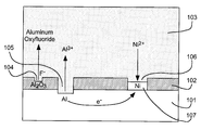
- FIG. 2 is a cross sectional view similar to FIG. 1, but illustrating the principal reactions of the fluoride-activated displacement plating process of the present invention when the reactive metal is aluminum and the stable metal is nickel.
- FIG. 3 is a cross sectional view similar to FIG. 2, but further depicting the uniform displacement coating of stable metal resulting from the displacement process of the present invention.
- FIG. 4 is a cross sectional view similar to FIG. 3, but further depicting an additional layer of stable metal applied to render the coating more solderable, wire bondable, and resistant to oxidation and corrosion.
- FIG. 5 is a cross sectional view similar to FIG. 4, but further depicting an additional noble metal layer applied to preserve the solderability and wire bondability of the overall coating.
- FIG. 1 is a cross sectional view of a highly reactive metal substrate 101 with a thick surface oxide layer 102 , which tends to increase in thickness with time under ambient or processing conditions.
- Surface oxide layer 102 is not wetted by commonly-available solders (not shown) and must be removed or penetrated if a solder connection or wire bond to reactive metal substrate 101 is to be formed.
- a thick surface oxide layer 102 which can result from long storage or previous processing, may be difficult to penetrate so that a sufficiently strong wire bond cannot be formed under normal wire bonding conditions.
- FIG. 2 is a cross sectional view illustrating fluoride-activated direct displacement plating according to the present invention when aluminum (Al) is the highly reactive metal of substrate 101 and nickel (Ni) is the relatively stable metal deposited by displacement plating.
- Al aluminum
- Ni nickel
- FIG. 2 is a cross sectional view illustrating fluoride-activated direct displacement plating according to the present invention when aluminum (Al) is the highly reactive metal of substrate 101 and nickel (Ni) is the relatively stable metal deposited by displacement plating.
- Al aluminum oxide
- Ni nickel
- oxide layer 102 completely dissolves and islands of stable metal, such as island 107 , grow and coalesce into a continuous layer.
- the solution 103 includes the following components:
- a solvent either nonaqueous, aqueous or mixtures thereof.
- Preferred solvents include dimethylsulfoxide (DMSO), ethylene glycol (EG), and other organic liquids.
- DMSO dimethylsulfoxide
- EG ethylene glycol
- H 2 ethylene glycol
- the preferred DMSO and EG nonaqueous solvents are less volatile than water so that higher temperatures can be used to accelerate the rates of the oxide dissolution and displacement reactions.
- water may be present in appreciable amounts in nonaqueous systems without degrading the quality of displacement coating obtained. Insensitivity to the presence of water is highly beneficial for a practical process.
- a fluoride activator species to dissolve surface oxide layer 102 so that the displacement reaction can occur at a practical rate.
- Hydroxide is used as an activator for the zincating process of the prior art but has been found to be too aggressive and difficult to control, and typically cannot be used in anhydrous nonaqueous solvents. Hydroxide usually cannot be used for nickel displacement plating since Ni(OH) 2 is highly insoluble and would precipitate from most solutions. Nickel amine complexes are stable in the presence of hydroxide ion but do not displacement plate nickel on aluminum.
- the fluoride activator of the present invention can be added as a simple fluoride salt or in the form of an complex fluoroanion, which yields fluoride by dissociation.
- Nickel, cobalt and palladium are relatively oxidation-resistant and can be used as solderable finishes for electronics applications.
- Displacement coatings of all three metals have been applied to aluminum substrates by the displacement process of the present invention.
- a thin overlayer of noble metal, e.g., gold, may be used to preserve the solderability and wire bondability of nickel and cobalt coatings.
- the preferred solution anions are halides (chloride, bromide and iodide) or pseudohalides (cyanide and thiocyanate), which tend to beneficially inhibit the displacement process by complexing the stable metal ions and adsorbing on the metal surface. Of these, chloride and bromide are most useful, since complexes of other halide and pseudohalide anions tend to lack sufficient solubility or stability, or form overly stable complexes that would slow the displacement reaction excessively.
- a key feature of the present invention is the use of an activator concentration gradient to minimize attack of the reactive metal substrate 101 by the fluoride activator species used to dissolve the recalcitrant surface oxide layer 102 .
- diffusion control of the activator is provided by utilizing a relatively low molar concentration of activator species (typically less than 0.10 M) in combination with minimal or no stirring of solution 103 .
- activator is consumed rapidly by reaction with surface oxide 102 , its concentration in the vicinity of the interface with solution 103 decreases sharply because its replenishment is limited by diffusion, which is a relatively slow process.
- Activator depletion within pores is even more dramatic since the activator also reacts with the sides of the pores, and the solution within the pores is small in volume and stagnant.
- substrate 101 is effectively protected from dissolution produced by the activator, which consumes substrate material without contributing to the displacement plating process.
- a high molar concentration of stable metal ions (>1.0 M Ni 2+ ) is used in solution 103 to avoid significant depletion of such ions within pores in surface oxide 102 , which would appreciably slow the displacement process. Since competing reactions are involved, the optimum concentrations for the activator species and stable metal ions depends greatly on the solvent, stable metal type, anion type, and solution temperature and level of agitation. For example, palladium ions are generally more easily reduced than nickel or cobalt ions so that the optimum palladium ion concentration is typically lower, and a lower activator concentration may be beneficial as well.
- An effective activator concentration gradient for minimizing attack of substrate 101 may also be attained under forced convection conditions. For example, non-turbulent solution flow or part movement parallel with the substrate 101 surface would tend to reduce the activator gradient at the surface of oxide layer 102 but not appreciably within pores 104 , 105 and 106 so that attack of substrate 101 would still be minimized. In this case, the enhanced dissolution rate of surface oxide 102 would have to be taken into account via appropriate modifications in the solution composition or operating conditions.
- Vigorous bath agitation via gas sparging or solution pumping is normally specified by plating bath suppliers as necessary to replenish bath constituents at the part surface as they are consumed in plating reactions. With too little bath agitation, plated deposits tend to be powdery and non-adherent.
- Solution 103 is typically maintained at an elevated temperature in the range from 50° to 150° C. to provide practical rates for the oxide dissolution and displacement reactions. Uniform heating of the solution is preferred to minimize convection that would increase the rate of activator transport and attack of substrate 101 . Uniform heating can be attained by utilizing a heating surface having a large area and good heat transfer so that the temperature differential relative to the solution is small. Solution stirring via convection can also be minimized by preheating the part prior to immersion in solution 103 .
- vibrations arising from external sources may need to be suppressed via appropriate dampening.
- Baffling could also be installed to hinder solution motion arising from external sources or to dampen solution motion resulting from insertion or removal of parts containing the reactive metal to be plated.
- FIG. 3 is a cross sectional view depicting a continuous layer of stable metal 108 formed on reactive metal substrate 101 according to the present invention. Since deposition of the stable metal is driven by dissolution of the reactive metal in substrate 101 , stable metal layer 108 is necessarily thin, has a roughened surface texture compared to the original active metal substrate, and contains traversing micropores 109 . For these reasons, it is generally desirable to increase the thickness of stable metal to enhance or preserve wire bondability, solderability, and oxidation/corrosion resistance. Nonetheless, displacement layer 108 can be several monolayers thick as a result of localized dissolution of multiple layers of reactive metal, as well as the extra electrons on a per atom basis provided by dissolution of higher valence reactive metal.
- FIG. 4 is a cross sectional view depicting reactive metal substrate 101 coated with stable metal layer 108 applied by displacement plating, and an additional layer 110 of stable metal.
- Layers 108 and 110 could be comprised of different metals but this would normally not be advantageous.
- nickel is preferably used for layer 108 and for layer 110 .
- the latter is preferably applied by electroless plating rather than by electroplating to avoid the need for an electrical connection to the pads. Thick deposits with low porosity for layer 110 can be provided by either approach.
- FIG. 5 shows the addition of a thin noble metal layer 111 to the coating depicted in FIG. 4 .
- the noble metal layer protects the coating from oxidation and/or corrosion. Such a layer is necessary to prevent loss of solderability and wire bondability of nickel-coated aluminum pads on IC chips.
- layer 111 is preferably gold applied by displacement plating or electroless plating, which avoids the need for electrical contact to the pads. A thicker coating providing greater protection could be applied by electroplating.
- Other noble metals that could be used include platinum (Pt), iridium (Ir), osmium (Os), palladium (Pd), rhenium (Re), rhodium (Rh), and ruthenium (Ru).
- Water rinses are generally effective for the process of the present invention. To avoid buildup of water from a prior aqueous rinse, parts should be dried before being brought into contact with a nonaqueous displacement solution. Drying may be performed by any standard method, including air drying, blow drying, and/or heating the part.
- the displacement plating process of the present invention is particularly advantageous for applying a stable metal coating to aluminum pads on IC chips and substrates to render them solderable or to preserve or restore their wire bondability.
- nickel is the obvious choice for the stable metal since it is already widely used as a solderable/bondable surface finish (with a thin overlayer of gold), and the electroless plating process needed to increase the deposit thickness is well established.
- Cobalt and palladium have also been deposited directly on aluminum by the displacement plating process of the present invention and could be substituted for nickel in many applications. Palladium offers the advantage of being highly resistant to oxidation so that an overlayer of noble metal is not required to preserve solderability/bondability. It is also an effective nucleation catalyst for electroless deposition of most metals, including nickel and cobalt.
- the zincating/electroless nickel process currently used to improve the corrosion and wear resistance of aluminum and its alloys for structural applications suffers from many disadvantages (as discussed above) that could be obviated by use of the nickel displacement process of the present invention.
- This displacement plating process could also be employed to enhance the stability and properties of other reactive structural metals including titanium, magnesium, beryllium, and alloys thereof.
- the displacement coated part may be used directly but it is typically advantageous to apply additional stable metal, preferably by electroless plating, which avoids the need to make electrical contact. Electroplating or vacuum deposition could be used.
- the preferred approach is to rapidly rinse the part in water maintained at approximately 100° C., in which oxygen is only sparingly soluble.
- the direct displacement plating solution of the present invention comprises a solvent, a fluoride activator to dissolve the recalcitrant oxide on the reactive metal substrate, and a source of stable metal ions.
- Preferred solvents are dimethylsulfoxide (DMSO), ethylene glycol (EG), and other organic liquids in which appropriate stable metal ions and fluorine activator compounds are soluble and stable.
- DMSO dimethylsulfoxide
- EG ethylene glycol
- Likely candidates are other alcohols and sulfur-containing compounds. Water present in such nonaqueous solvents is apparently not detrimental but use of pure water as the solvent does not produce the best displacement coatings.
- the reactivity of the fluoride activator and the stable metal ions must be optimized so as to balance the series reactions of oxide dissolution and displacement plating, while minimizing competing dissolution of the active metal substrate by the activator.
- oxide dissolution should be the slow step in the overall process so that displacement plating of the stable metal occurs immediately as new substrate surface is exposed, which minimizes the opportunity for substrate attack by the activator.
- the reactivity of the activator must be sufficiently high that the rate-limiting oxide dissolution step is fast enough for a practical process, but not so high that excessive substrate dissolution occurs through pores in the oxide.
- the inherent reactivity of the stable metal ions must be high enough that the displacement reaction keeps up with the oxide dissolution reaction, but must not be so high that the displacement process is uncontrolled and produces powdery deposits. Since both of these reactivities depend on several interdependent variables (e.g., solvent type, specific reactive/stable metal pair involved, reactant concentrations, solution temperature, agitation level, and anion type), there are numerous combinations of variables that will, in principle, yield optimum coating quality. Nonetheless, definite operating ranges or limits, can be delineated for direct displacement plating of a given stable metal on aluminum from one of the preferred solvents at 100° C. containing halide anions and the preferred fluoride activator species.
- Preferred anions for the displacement plating solution are halides (chloride, bromide and iodide) and pseudohalides (cyanide and thiocyanate), which form salts with nickel, cobalt and palladium ions that are highly soluble in the appropriate solvents and are readily rendered anhydrous by heating.
- chloride and bromide are preferred since they provide the moderately strong complexes with the stable metal cations that are beneficial to the displacement coating quality but do not excessively slow the displacement plating process.
- agitation within pores in the surface oxide layer on the active metal substrate is preferably minimized so that the activator species becomes depleted by reaction with the oxide, which reduces the rate of dissolution of the substrate by the activator.
- laminar solution flow or part movement parallel to the surface could enhance solution mass transport to the surface without perturbing the solution in pores but can be difficult to attain uniformly over the part surface and to maintain constant with time.
- the preferred approach is to maintain the solution in a relatively quiescent state, which presents little practical difficulty.
- the concentration of activator at exposed substrate areas within surface oxide pores is minimized by using both a low concentration of activator species and little or no solution agitation.
- a useful non-hygroscopic fluoride salt is TRIS.HF, which can be synthesized by reaction of tris(hydroxymethyl)aminomethane with hydrofluoric acid (HF), followed by evaporation of the water present.
- the optimum molar concentration of the fluoride activator species is generally less than 0.10 M, and typically less than 0.05 M.
- the reducibility of the specific stable metal ions involved must be taken into account.
- nickel and cobalt chlorides which are not easily reduced, can be used at very high concentrations (>2.0 M) and a concentration of 1.0 M or more is preferred.
- the molar concentration of the [(C 2 H 5 ) 4 N] 2 PdCl 4 salt used to plate on aluminum from DMSO at 100° C. had to be limited to not more than 0.15 M to avoid uncontrolled displacement.
- a pretreatment in a cleaning/conditioning solution is desirable to improve the consistency and uniformity of the subsequent displacement coating.
- Good results have been obtained for a pretreatment of 5 to 10 seconds in a “bright dipping” solution at 50° C. comprised of 80% phosphoric acid, 5% nitric acid, 5% acetic acid and 10% water (by volume).
- Water rinsing of the part prior to exposure to each of the processing solutions is recommended to avoid buildup of contaminants in the solutions. Drying parts before displacement plating is desirable to avoid buildup of water in nonaqueous solutions.
- the DMSO solvent Aldrich Chemical, 99.9% spectrophotometric grade
- the EG solvent Aldrich, 99.8% anhydrous
- Anhydrous NiCl 2 and CoCl 2 were obtained by drying the hexahydrate salts at 120° C. for several hours.
- Ni(en) 3 SiF 6 salt was synthesized by the following procedure. A mixture of 30 mmole of NiF 2 .4H 2 O and 90 mmole of ethylenediamine (en) was stirred overnight in 150 mL of methanol. To this filtered solution was added with stirring a solution of H 2 SiF 6 made from the reaction of 30 mmole of tetraethylorthosilicate (TEOS) with 180 mmole of 48% aqueous HF in 50 mL of methanol. The resulting mixture was diluted to 400 mL with methanol and stirred overnight at room temperature. The precipitate was filtered, rinsed with isopropanol, and dried to yield 28.8 mmole (96%) of Ni(en) 3 SiF 6 as a non-hygroscopic pink powder.
- TEOS tetraethylorthosilicate
- the [(CH 3 ) 4 N] 2 SiF 6 salt was prepared in quantitative yield by evaporation at 60° C. of a mixture of H 2 SiF 6 , from TEOS and excess aqueous HF, with a stoichiometric amount of (CH 3 ) 4 NF.4H 2 O in a plastic beaker.
- the resulting white hygroscopic crystalline solid was stirred in acetone, filtered, air-dried, and stored in a sealed vessel.
- the [(C 2 H 5 ) 4 N] 2 PdCl 4 salt was prepared by dissolving stoichiometric amounts of PdCl 2 and tetraethylammonium chloride in concentrated HCl and evaporating the solution to dryness at 60° C. The residue was stirred in hot isopropanol and filtered to give a nearly quantitative yield of the chloro complex salt as a fine brown non-hygroscopic crystalline powder. In hot EG, the PdCl 4 2 ⁇ anion decomposes to form elemental Pd 0 , which precludes use of this solvent in this case.
- a silicon IC test chip was treated for 10 minutes in a quiescent EG solution containing 2.0 M NiCl 2 and 0.03 M [(CH 3 ) 4 N] 2 SiF 6 (at about 100° C.), and then successively in electroless nickel and immersion gold baths.
- the chip pads were uniformly coated with adherent layers of nickel and gold.
- the NiCl 2 remained in solution.
- a silicon IC test chip was treated for 10 minutes in a quiescent DMSO solution containing 2.0 M CoCl 2 and 0.03 M [(CH 3 ) 4 N] 2 SiF 6 (at about 100° C.), and then successively in electroless nickel and immersion gold baths.
- the chip pads were uniformly coated with adherent layers of cobalt, nickel and gold, as observed microscopically.
- a silicon IC test chip was treated for 10 minutes in a quiescent EG solution containing 2.0 M CoCl 2 and 0.03 M [(CH 3 ) 4 N] 2 SiF 6 (at about 100° C.), and then successively in electroless nickel and immersion gold baths.
- the chip pads were uniformly coated with adherent layers of cobalt, nickel and gold, as observed microscopically.
- a silicon IC test chip was treated for 60 seconds in a quiescent EG solution containing 0.15 M [(C 2 H 5 ) 4 N] 2 PdCl 4 and 0.03 M [(CH 3 ) 4 N] 2 SiF 6 (at about 100° C.), and then successively in electroless nickel and immersion gold baths.
- the chip pads were uniformly coated with adherent layers of palladium, nickel and gold.
- a silicon IC test chip was treated for 18 minutes in a quiescent EG solution containing 2.0 M NiCl 2 and 0.02 M TRIS.HF (at about 100° C.), and then successively in electroless nickel and immersion gold baths.
- the chip pads were uniformly coated with adherent layers of nickel and gold.
- Silicon IC test chips from a different batch were treated as in example 1 but in this case the displacement coating quality varied greatly from pad to pad. Some pads were acceptably coated whereas others were practically uncoated or coated only in some areas. Other chips from this batch were pretreated for 5 to 10 seconds in a “bright dipping” solution at 50° C. comprised of 80% phosphoric acid, 5% nitric acid, 5% acetic acid and 10% water (by volume), and were then rinsed in water and blow dried with nitrogen prior to nickel displacement plating. In this case, good consistency and uniformity of the nickel displacement coating, and subsequent electroless nickel and gold layers, were observed.
- the direct displacement plating process of the present invention provides a uniform, adherent coating of a more stable metal on a reactive metal substrate that is normally covered with a recalcitrant surface oxide. It can be used to apply nickel, cobalt and palladium coatings on aluminum, and presumably on aluminum alloys. It should also be applicable to other reactive metals, including titanium, magnesium, beryllium, and alloys thereof.
- Direct displacement plating of nickel on aluminum IC chip pads according to the present invention provides a solderable surface without the need for expensive masks and vacuum deposition processes.
- Such a maskless bumping process offers substantial cost savings.
- a thin layer of gold is applied by displacement or electroless plating to protect the nickel coating from oxidation prior to and during the solder bumping operation.
- This nickel/gold coating can also be used to preserve or restore wire bondability of the aluminum IC chip pads.
- the displacement plating solution of the present invention comprises a solvent (preferably dimethylsulfoxide or ethylene glycol), a salt that supplies ions of the stable metal (preferably a halide or pseudohalide), and an activator that reacts to dissolve the recalcitrant oxide on the reactive metal substrate.
- a solvent preferably dimethylsulfoxide or ethylene glycol
- a salt that supplies ions of the stable metal (preferably a halide or pseudohalide)
- an activator that reacts to dissolve the recalcitrant oxide on the reactive metal substrate.
- An elevated temperature in the 50 to 150° C. range is typically needed to increase the rate of the overall displacement process, which requires about 10 minutes for completion. This reaction is self-limiting so that longer exposure to the solution is not detrimental.
- the overall displacement plating process involves the series reactions of oxide dissolution and displacement plating and the competing reaction of substrate dissolution by the fluoride activator.
- the relative rates of these reactions is very important to the coating quality but depend on the interdependent variables of solvent type, specific reactive/stable metal pair involved, reactant concentrations, solution temperature, agitation level, and anion type. Consequently, optimum operating conditions can be delineated only for a specific system for which some variables have been fixed.
- a key feature of this direct displacement process is the use of a fluoride activator to remove the surface oxide with minimal attack of the underlying reactive metal substrate. Such attack represents a competing side reaction that degrades the deposit quality, and must also be minimized to avoid excessive consumption of the thin aluminum pads on IC chips.
- the reactivity of the fluoride activator can be adjusted for a given solvent via judicious choice of the species used as a fluoride activator and its concentration. For example, the fluoride activity for a given concentration of various fluorine-containing anions decreases in the order: F ⁇ >AlF 6 3 ⁇ >SiF 6 2 ⁇ >>PF 6 ⁇ , BF 4 ⁇ for the dimethylsulfoxide solvent.
- Other potentially useful fluoroanions include the F 2 PO 2 ⁇ and FSO 3 ⁇ anions.
Abstract
Description
Claims (32)
Priority Applications (1)
| Application Number | Priority Date | Filing Date | Title |
|---|---|---|---|
| US09/658,643 US6503343B1 (en) | 2000-09-11 | 2000-09-11 | Controlled plating on reactive metals |
Applications Claiming Priority (1)
| Application Number | Priority Date | Filing Date | Title |
|---|---|---|---|
| US09/658,643 US6503343B1 (en) | 2000-09-11 | 2000-09-11 | Controlled plating on reactive metals |
Publications (1)
| Publication Number | Publication Date |
|---|---|
| US6503343B1 true US6503343B1 (en) | 2003-01-07 |
Family
ID=24642076
Family Applications (1)
| Application Number | Title | Priority Date | Filing Date |
|---|---|---|---|
| US09/658,643 Expired - Lifetime US6503343B1 (en) | 2000-09-11 | 2000-09-11 | Controlled plating on reactive metals |
Country Status (1)
| Country | Link |
|---|---|
| US (1) | US6503343B1 (en) |
Cited By (16)
| Publication number | Priority date | Publication date | Assignee | Title |
|---|---|---|---|---|
| US20040084773A1 (en) * | 2002-10-31 | 2004-05-06 | Johnston Steven W. | Forming a copper diffusion barrier |
| US20040157440A1 (en) * | 2002-05-24 | 2004-08-12 | Gleason Jeffery N. | Using stabilizers in electroless solutions to inhibit plating of fuses |
| US20060046088A1 (en) * | 2004-09-02 | 2006-03-02 | Salman Akram | Selective nickel plating of aluminum, copper, and tungsten structures |
| US20070287225A1 (en) * | 2006-06-02 | 2007-12-13 | Infineon Technologies Ag | Method of Manufacturing an Integrated Circuit |
| WO2008011256A1 (en) * | 2006-07-19 | 2008-01-24 | Gm Global Technology Operations, Inc. | METHOD OF MAKING NiO AND Ni NANOSTRUCTURES |
| US20080152823A1 (en) * | 2006-12-20 | 2008-06-26 | Lam Research Corporation | Self-limiting plating method |
| WO2008130592A1 (en) * | 2007-04-18 | 2008-10-30 | Ovonic Battery Company, Inc. | Process for producing hydrogen gas from sustainable biofuels or from other carbon based fuels |
| CN100451170C (en) * | 2006-11-21 | 2009-01-14 | 东北大学 | Process for preparing pretreatment layer and coating on magnesium and magnesium alloy surface |
| US20110129607A1 (en) * | 2009-12-01 | 2011-06-02 | Samsung Electro-Mechanics Co., Ltd. | Substitutional electroless gold plating solution and method for forming gold plating layer using the same |
| CN102703910A (en) * | 2012-05-25 | 2012-10-03 | 浙江吉利汽车研究院有限公司杭州分公司 | Hot working process for lowering hydrogen embrittlement |
| US20130224511A1 (en) * | 2012-02-24 | 2013-08-29 | Artur Kolics | Methods and materials for anchoring gapfill metals |
| DE102017213170A1 (en) * | 2017-07-31 | 2019-01-31 | Infineon Technologies Ag | SOLDERING A LADDER TO ALUMINUM METALLIZATION |
| US20190109104A1 (en) * | 2017-10-05 | 2019-04-11 | Texas Instruments Incorporated | Electronic device having coated contact pads |
| US10917966B2 (en) | 2018-01-29 | 2021-02-09 | Corning Incorporated | Articles including metallized vias |
| US10932371B2 (en) | 2014-11-05 | 2021-02-23 | Corning Incorporated | Bottom-up electrolytic via plating method |
| US20210375792A1 (en) * | 2020-05-29 | 2021-12-02 | Infineon Technologies Ag | Chip package and method of forming a chip package |
Citations (3)
| Publication number | Priority date | Publication date | Assignee | Title |
|---|---|---|---|---|
| US4018628A (en) * | 1974-10-18 | 1977-04-19 | Swiss Aluminium Ltd. | Process for coloring aluminium |
| US4235648A (en) * | 1979-04-05 | 1980-11-25 | Motorola, Inc. | Method for immersion plating very thin films of aluminum |
| US5993567A (en) * | 1995-01-13 | 1999-11-30 | Henkel Corporation | Compositions and processes for forming a solid adherent protective coating on metal surfaces |
-
2000
- 2000-09-11 US US09/658,643 patent/US6503343B1/en not_active Expired - Lifetime
Patent Citations (3)
| Publication number | Priority date | Publication date | Assignee | Title |
|---|---|---|---|---|
| US4018628A (en) * | 1974-10-18 | 1977-04-19 | Swiss Aluminium Ltd. | Process for coloring aluminium |
| US4235648A (en) * | 1979-04-05 | 1980-11-25 | Motorola, Inc. | Method for immersion plating very thin films of aluminum |
| US5993567A (en) * | 1995-01-13 | 1999-11-30 | Henkel Corporation | Compositions and processes for forming a solid adherent protective coating on metal surfaces |
Cited By (38)
| Publication number | Priority date | Publication date | Assignee | Title |
|---|---|---|---|---|
| US7687879B2 (en) | 2002-05-24 | 2010-03-30 | Micron Technology, Inc. | Intermediate semiconductor device structure |
| US20040157440A1 (en) * | 2002-05-24 | 2004-08-12 | Gleason Jeffery N. | Using stabilizers in electroless solutions to inhibit plating of fuses |
| US20040084773A1 (en) * | 2002-10-31 | 2004-05-06 | Johnston Steven W. | Forming a copper diffusion barrier |
| US7279423B2 (en) * | 2002-10-31 | 2007-10-09 | Intel Corporation | Forming a copper diffusion barrier |
| US10062608B2 (en) | 2004-09-02 | 2018-08-28 | Micron Technology, Inc. | Semiconductor devices comprising nickel- and copper-containing interconnects |
| US20090176362A1 (en) * | 2004-09-02 | 2009-07-09 | Micron Technology, Inc. | Methods of forming interconnects in a semiconductor structure |
| US7855454B2 (en) | 2004-09-02 | 2010-12-21 | Micron Technology, Inc. | Semiconductor device structures including nickel plated aluminum, copper, and tungsten structures |
| US20060046088A1 (en) * | 2004-09-02 | 2006-03-02 | Salman Akram | Selective nickel plating of aluminum, copper, and tungsten structures |
| US10446440B2 (en) | 2004-09-02 | 2019-10-15 | Micron Technology, Inc. | Semiconductor devices comprising nickel— and copper—containing interconnects |
| US8647982B2 (en) | 2004-09-02 | 2014-02-11 | Micron Technology, Inc. | Methods of forming interconnects in a semiconductor structure |
| US20070132105A1 (en) * | 2004-09-02 | 2007-06-14 | Salman Akram | Selective activation of aluminum, copper, and tungsten structures |
| US9640433B2 (en) | 2004-09-02 | 2017-05-02 | Micron Technology, Inc. | Methods of forming interconnects and semiconductor structures |
| US20070004200A1 (en) * | 2004-09-02 | 2007-01-04 | Salman Akram | Selective activation of aluminum, copper, and tungsten structures |
| US7279407B2 (en) | 2004-09-02 | 2007-10-09 | Micron Technology, Inc. | Selective nickel plating of aluminum, copper, and tungsten structures |
| US20070287225A1 (en) * | 2006-06-02 | 2007-12-13 | Infineon Technologies Ag | Method of Manufacturing an Integrated Circuit |
| US7579268B2 (en) * | 2006-06-02 | 2009-08-25 | Infineon Technologies Ag | Method of manufacturing an integrated circuit |
| WO2008011256A1 (en) * | 2006-07-19 | 2008-01-24 | Gm Global Technology Operations, Inc. | METHOD OF MAKING NiO AND Ni NANOSTRUCTURES |
| CN100451170C (en) * | 2006-11-21 | 2009-01-14 | 东北大学 | Process for preparing pretreatment layer and coating on magnesium and magnesium alloy surface |
| WO2008085261A1 (en) * | 2006-12-20 | 2008-07-17 | Lam Research Corporation | Self-limiting plating method |
| US20080152823A1 (en) * | 2006-12-20 | 2008-06-26 | Lam Research Corporation | Self-limiting plating method |
| WO2008130592A1 (en) * | 2007-04-18 | 2008-10-30 | Ovonic Battery Company, Inc. | Process for producing hydrogen gas from sustainable biofuels or from other carbon based fuels |
| US20110129607A1 (en) * | 2009-12-01 | 2011-06-02 | Samsung Electro-Mechanics Co., Ltd. | Substitutional electroless gold plating solution and method for forming gold plating layer using the same |
| US20130224511A1 (en) * | 2012-02-24 | 2013-08-29 | Artur Kolics | Methods and materials for anchoring gapfill metals |
| US8895441B2 (en) * | 2012-02-24 | 2014-11-25 | Lam Research Corporation | Methods and materials for anchoring gapfill metals |
| US9382627B2 (en) | 2012-02-24 | 2016-07-05 | Lam Research Corporation | Methods and materials for anchoring gapfill metals |
| CN102703910A (en) * | 2012-05-25 | 2012-10-03 | 浙江吉利汽车研究院有限公司杭州分公司 | Hot working process for lowering hydrogen embrittlement |
| CN102703910B (en) * | 2012-05-25 | 2014-09-10 | 浙江吉利汽车研究院有限公司杭州分公司 | Hot working process for lowering hydrogen embrittlement |
| US10932371B2 (en) | 2014-11-05 | 2021-02-23 | Corning Incorporated | Bottom-up electrolytic via plating method |
| DE102017213170A1 (en) * | 2017-07-31 | 2019-01-31 | Infineon Technologies Ag | SOLDERING A LADDER TO ALUMINUM METALLIZATION |
| US10615145B2 (en) | 2017-07-31 | 2020-04-07 | Infineon Technologies Ag | Soldering a conductor to an aluminum metallization |
| US10896893B2 (en) | 2017-07-31 | 2021-01-19 | Infineon Technologies Ag | Soldering a conductor to an aluminum metallization |
| US11450642B2 (en) | 2017-07-31 | 2022-09-20 | Infineon Technologies Ag | Soldering a conductor to an aluminum metallization |
| US20190109104A1 (en) * | 2017-10-05 | 2019-04-11 | Texas Instruments Incorporated | Electronic device having coated contact pads |
| US10714439B2 (en) * | 2017-10-05 | 2020-07-14 | Texas Instruments Incorporated | Electronic device having cobalt coated aluminum contact pads |
| US10917966B2 (en) | 2018-01-29 | 2021-02-09 | Corning Incorporated | Articles including metallized vias |
| US20210375792A1 (en) * | 2020-05-29 | 2021-12-02 | Infineon Technologies Ag | Chip package and method of forming a chip package |
| US11735534B2 (en) * | 2020-05-29 | 2023-08-22 | Infineon Technologies Ag | Chip package and method of forming a chip package |
| US20230395532A1 (en) * | 2020-05-29 | 2023-12-07 | Infineon Technologies Ag | Chip package and method of forming a chip package |
Similar Documents
| Publication | Publication Date | Title |
|---|---|---|
| US6503343B1 (en) | Controlled plating on reactive metals | |
| EP0795043B1 (en) | Silver plating | |
| US6395329B2 (en) | Printed circuit board manufacture | |
| EP1322798B1 (en) | Bath and method of electroless plating of silver on metal surfaces | |
| US6319543B1 (en) | Process for silver plating in printed circuit board manufacture | |
| CN1094799C (en) | Palladium immersion deposition to selectively initiate electroless plating on Ti and W alloys for wafer fabrication | |
| JP5283903B2 (en) | Silver plating in electronic component manufacturing | |
| JP3892730B2 (en) | Electroless gold plating solution | |
| WO2004067192A1 (en) | Electroless plating solution and process | |
| JP2009512784A (en) | Compositions and methods for improving adhesion of polymeric materials to copper or copper alloy surfaces | |
| JP2008169425A (en) | Method for maintaining plating capability of electroless gold-plating bath | |
| JP2008144187A (en) | Electroless gold plating bath, electroless gold plating method, and electronic component | |
| US6336962B1 (en) | Method and solution for producing gold coating | |
| JP3337802B2 (en) | Direct plating method by metallization of copper (I) oxide colloid | |
| KR100619345B1 (en) | Method for plating on printed circuit board for semi-conductor package and printed circuit board produced therefrom | |
| US20040234777A1 (en) | Method for electroless plating without precious metal sensitization | |
| JP2005529241A (en) | Acidic solution for silver deposition and method for depositing a silver layer on a metal surface | |
| JP7407644B2 (en) | Palladium plating solution and plating method | |
| JPH06101054A (en) | Catalyst liquid selective of copper-base material for electroless plating | |
| JPH09510411A (en) | Copper bismuth coating protection | |
| JP4059133B2 (en) | Electroless nickel-gold plating method |
Legal Events
| Date | Code | Title | Description |
|---|---|---|---|
| AS | Assignment |
Owner name: ROCKWELL TECHNOLOGIES, LLC, CALIFORNIA Free format text: ASSIGNMENT OF ASSIGNORS INTEREST;ASSIGNORS:TENCH, D. MORGAN;WARREN, L.F. JR.;WHITE, JOHN T.;REEL/FRAME:011198/0793 Effective date: 20000908 |
|
| STCF | Information on status: patent grant |
Free format text: PATENTED CASE |
|
| FPAY | Fee payment |
Year of fee payment: 4 |
|
| AS | Assignment |
Owner name: ROCKWELL SCIENTIFIC LICENSING, LLC, CALIFORNIA Free format text: CHANGE OF NAME;ASSIGNOR:INNOVATIVE TECHNOLOGY LICENSING, LLC;REEL/FRAME:018160/0250 Effective date: 20030919 Owner name: INNOVATIVE TECHNOLOGY LICENSING, LLC, CALIFORNIA Free format text: CHANGE OF NAME;ASSIGNOR:ROCKWELL TECHNOLOGIES, LLC;REEL/FRAME:018160/0240 Effective date: 20010628 |
|
| AS | Assignment |
Owner name: TELEDYNE LICENSING, LLC, CALIFORNIA Free format text: CHANGE OF NAME;ASSIGNOR:ROCKWELL SCIENTIFIC LICENSING, LLC;REEL/FRAME:018573/0649 Effective date: 20060918 |
|
| FEPP | Fee payment procedure |
Free format text: PAYOR NUMBER ASSIGNED (ORIGINAL EVENT CODE: ASPN); ENTITY STATUS OF PATENT OWNER: LARGE ENTITY |
|
| AS | Assignment |
Owner name: ASTRIPHEY APPLICATIONS, L.L.C., DELAWARE Free format text: ASSIGNMENT OF ASSIGNORS INTEREST;ASSIGNOR:TELEDYNE LICENSING, LLC;REEL/FRAME:022392/0211 Effective date: 20090129 |
|
| FPAY | Fee payment |
Year of fee payment: 8 |
|
| FPAY | Fee payment |
Year of fee payment: 12 |
|
| AS | Assignment |
Owner name: CALLAHAN CELLULAR L.L.C., DELAWARE Free format text: MERGER;ASSIGNOR:ASTRIPHEY APPLICATIONS L.L.C.;REEL/FRAME:037509/0695 Effective date: 20150826 |