US6504267B1 - Flyback power converter with secondary-side control and primary-side soft switching - Google Patents
Flyback power converter with secondary-side control and primary-side soft switching Download PDFInfo
- Publication number
- US6504267B1 US6504267B1 US10/017,346 US1734601A US6504267B1 US 6504267 B1 US6504267 B1 US 6504267B1 US 1734601 A US1734601 A US 1734601A US 6504267 B1 US6504267 B1 US 6504267B1
- Authority
- US
- United States
- Prior art keywords
- switch
- primary
- output
- power
- voltage
- Prior art date
- Legal status (The legal status is an assumption and is not a legal conclusion. Google has not performed a legal analysis and makes no representation as to the accuracy of the status listed.)
- Expired - Fee Related
Links
- 238000004804 winding Methods 0.000 claims abstract description 26
- 239000003990 capacitor Substances 0.000 claims abstract description 12
- 230000033228 biological regulation Effects 0.000 claims description 14
- 230000001105 regulatory effect Effects 0.000 abstract description 15
- 238000002955 isolation Methods 0.000 abstract description 4
- 238000000034 method Methods 0.000 description 14
- 238000010586 diagram Methods 0.000 description 6
- 230000003071 parasitic effect Effects 0.000 description 4
- 230000008901 benefit Effects 0.000 description 2
- 230000000903 blocking effect Effects 0.000 description 2
- 238000006243 chemical reaction Methods 0.000 description 1
- 238000010276 construction Methods 0.000 description 1
- 230000001276 controlling effect Effects 0.000 description 1
- 230000007812 deficiency Effects 0.000 description 1
- 230000000694 effects Effects 0.000 description 1
- 230000005669 field effect Effects 0.000 description 1
- 230000020169 heat generation Effects 0.000 description 1
- 230000005415 magnetization Effects 0.000 description 1
- 229910044991 metal oxide Inorganic materials 0.000 description 1
- 150000004706 metal oxides Chemical class 0.000 description 1
- 238000012986 modification Methods 0.000 description 1
- 230000004048 modification Effects 0.000 description 1
- 238000012544 monitoring process Methods 0.000 description 1
- 230000003287 optical effect Effects 0.000 description 1
- 230000008569 process Effects 0.000 description 1
- 239000004065 semiconductor Substances 0.000 description 1
- 238000012163 sequencing technique Methods 0.000 description 1
- 239000013589 supplement Substances 0.000 description 1
- 230000007704 transition Effects 0.000 description 1
Images


Classifications
-
- H—ELECTRICITY
- H02—GENERATION; CONVERSION OR DISTRIBUTION OF ELECTRIC POWER
- H02M—APPARATUS FOR CONVERSION BETWEEN AC AND AC, BETWEEN AC AND DC, OR BETWEEN DC AND DC, AND FOR USE WITH MAINS OR SIMILAR POWER SUPPLY SYSTEMS; CONVERSION OF DC OR AC INPUT POWER INTO SURGE OUTPUT POWER; CONTROL OR REGULATION THEREOF
- H02M3/00—Conversion of dc power input into dc power output
- H02M3/22—Conversion of dc power input into dc power output with intermediate conversion into ac
- H02M3/24—Conversion of dc power input into dc power output with intermediate conversion into ac by static converters
- H02M3/28—Conversion of dc power input into dc power output with intermediate conversion into ac by static converters using discharge tubes with control electrode or semiconductor devices with control electrode to produce the intermediate ac
- H02M3/325—Conversion of dc power input into dc power output with intermediate conversion into ac by static converters using discharge tubes with control electrode or semiconductor devices with control electrode to produce the intermediate ac using devices of a triode or a transistor type requiring continuous application of a control signal
- H02M3/335—Conversion of dc power input into dc power output with intermediate conversion into ac by static converters using discharge tubes with control electrode or semiconductor devices with control electrode to produce the intermediate ac using devices of a triode or a transistor type requiring continuous application of a control signal using semiconductor devices only
- H02M3/33561—Conversion of dc power input into dc power output with intermediate conversion into ac by static converters using discharge tubes with control electrode or semiconductor devices with control electrode to produce the intermediate ac using devices of a triode or a transistor type requiring continuous application of a control signal using semiconductor devices only having more than one ouput with independent control
-
- H—ELECTRICITY
- H02—GENERATION; CONVERSION OR DISTRIBUTION OF ELECTRIC POWER
- H02M—APPARATUS FOR CONVERSION BETWEEN AC AND AC, BETWEEN AC AND DC, OR BETWEEN DC AND DC, AND FOR USE WITH MAINS OR SIMILAR POWER SUPPLY SYSTEMS; CONVERSION OF DC OR AC INPUT POWER INTO SURGE OUTPUT POWER; CONTROL OR REGULATION THEREOF
- H02M3/00—Conversion of dc power input into dc power output
- H02M3/22—Conversion of dc power input into dc power output with intermediate conversion into ac
- H02M3/24—Conversion of dc power input into dc power output with intermediate conversion into ac by static converters
- H02M3/28—Conversion of dc power input into dc power output with intermediate conversion into ac by static converters using discharge tubes with control electrode or semiconductor devices with control electrode to produce the intermediate ac
- H02M3/325—Conversion of dc power input into dc power output with intermediate conversion into ac by static converters using discharge tubes with control electrode or semiconductor devices with control electrode to produce the intermediate ac using devices of a triode or a transistor type requiring continuous application of a control signal
- H02M3/335—Conversion of dc power input into dc power output with intermediate conversion into ac by static converters using discharge tubes with control electrode or semiconductor devices with control electrode to produce the intermediate ac using devices of a triode or a transistor type requiring continuous application of a control signal using semiconductor devices only
-
- Y—GENERAL TAGGING OF NEW TECHNOLOGICAL DEVELOPMENTS; GENERAL TAGGING OF CROSS-SECTIONAL TECHNOLOGIES SPANNING OVER SEVERAL SECTIONS OF THE IPC; TECHNICAL SUBJECTS COVERED BY FORMER USPC CROSS-REFERENCE ART COLLECTIONS [XRACs] AND DIGESTS
- Y02—TECHNOLOGIES OR APPLICATIONS FOR MITIGATION OR ADAPTATION AGAINST CLIMATE CHANGE
- Y02B—CLIMATE CHANGE MITIGATION TECHNOLOGIES RELATED TO BUILDINGS, e.g. HOUSING, HOUSE APPLIANCES OR RELATED END-USER APPLICATIONS
- Y02B70/00—Technologies for an efficient end-user side electric power management and consumption
- Y02B70/10—Technologies improving the efficiency by using switched-mode power supplies [SMPS], i.e. efficient power electronics conversion e.g. power factor correction or reduction of losses in power supplies or efficient standby modes
Definitions
- the present invention relates in general, to power conversion and, more specifically, to a multiple output flyback converter, having improved cross-regulation and soft-switching to eliminate switching losses in the converter.
- Power converters are widely used to provide required voltages and load currents especially in environments that have higher concentrations of telecommunications or computer equipment. These power converters are often required to provide higher levels of output power for a small physical volume, since space is often at a premium. This requirement dictates that the power converters be high power density devices. These higher power density concentrations also dictate that the power converter operate with as high an efficiency as possible to minimize the converter's heat generation and therefore its operating temperature rise to the degree possible.
- One prior-art method for increasing power density of dc-to-dc converters, particularly in applications where more than one output voltage is required, is to use a single power stage with multiple windings on the power transformer, one for each output voltage.
- all outputs share the same inverter stage, and only one output, called the main output, is fully regulated by pulse-width modulation of the inverter switches on the primary side.
- Such a solution then requires feedback isolation, and additional post-regulators are required for independent regulation of the auxiliary outputs against load variation.
- the flyback converter is a very popular power supply topology for use in low-power,multiple output applications.
- these converters may be operated with the main output being regulated by the switching regulator and the other output (s) being “cross-regulated”, i.e., the ratio of the output voltages on the different windings is determined by the winding ratio and the actual relative voltage levels are determined by the ‘on’ time of the main switch.
- Cross-regulation of each output voltage is achieved by the turns ratio of the secondary windings.
- FIG. 1 illustrates a prior art flyback converter that uses a single switch on the primary side of the transformer to directly regulate one of the output voltage, i.e., Va, using feedback control.
- the cross-regulation of the other output voltages, i.e., Vb and Vc, is achieved by the turns ratio of the secondary winding.
- a drawback of the flyback converter of FIG. 1 is the presence of parasitics which result in wide tolerances for the cross-regulated outputs, which do not satisfy strict regulation requirements.
- Post-regulators e.g., linear regulators
- this approach increases cost and reduces efficiency of the power supply.
- a secondary side control method has been proposed as a solution to this shortcoming.
- FIG. 2 illustrates a flyback converter where a rectifying diode is connected in series with each secondary winding.
- the corresponding regulator RS 1 of the first output circuit controls the regulator (RS 0 ) of the primary-side circuit.
- Output regulators RS 2 , RS 3 control the secondary-side switches S 2 , S 3 correspondingly.
- the input DC voltage Vin, a voltage representation of the primary-side switch S 0 and one output of the regulators RS 2 , RS 3 are also fed to the primary-side regulator RS 0 .
- EP 0 772 284 discloses another secondary-side control method where one secondary winding supplies multiple output voltages via separate branches as shown in FIG. 3 .
- Each output voltage is rectified by means of a diode.
- the first output V 1 is regulated by the pulse width of the primary-sie switch S 0 .
- a switch is inserted into each branch supplying the rest of the output voltages (V 2 , V 3 ).
- a regulator senses each of the output voltages V 2 , V 3 .
- the regulator controls the duty cycle of the corresponding switch to regulate the output voltage.
- FIG. 4 illustrates a boost topology circuit configuration disclosed in Goder.
- voltage-regulator may be implemented with a flyback or other topologies.
- a dedicated switch to each output voltage controls the energy delivery to the output. Energy is delivered to only those outputs that have fallen below the lower limit of an acceptable range. The voltage regulator will stop supplying the outputs that have exceeded the upper limit of an acceptable range.
- European patents Nos. 0 698 959 and 0 772 284 and U.S. Pat. No. 5,617,015 to Goder each recite control of the on/off state of the primary-side switch based on the values of the output voltages. While each resolve the problem of primary side control of one of the outputs, they share a common drawback. Specifically, the secondary side control methods disclosed by each result in hard switching of the primary-side switch thus increasing switching losses and thereby reducing the efficiency of the power converter.
- a further drawback associated with the circuits of FIG. 2 and 3 is that one of the output voltages has no secondary-side switch dedicated to its regulation. Instead, the output includes a rectifying diode and is regulated by the primary side switch. This is problematic in reduced power modes of operation (e.g., standby) where it is desirable to disable some of the outputs. This cannot be achieved with the circuit configurations of FIGS. 2 and 3 because the output which does not include the secondary-side switch cannot be disabled without disabling all of the outputs.
- a still further drawback associated with the circuit of FIG. 4 is that the regulation method described therein increases the peak output current resulting in increased ripple compared with methods that continuously provide current to the multiple outputs.
- an objective of this invention is to make the converter insensitive to these parasitic effects by providing secondary-side control.
- a related objective of the present invention is to enable soft-switching of the primary side switch by taking advantage of the method of secondary-side control.
- the present invention provides, a circuit which combines secondary-side regulation with primary-side zero-volt switching to achieve a level of circuit efficiency and flexibility not available in prior art circuit constructions.
- the novel circuit provides circuit efficiency by providing zero-volt switching of the primary side switch. Zero-volt switching is achieved by taking advantage of a resonance which occurs between a switch capacitor coupled in parallel with a primary side power switch and a magnetization inductance of a primary side winding.
- a primary side controller detects the resonance condition and switches the power switch at one of the resonant waveform minima.
- the novel circuit further provides flexibility via secondary-side regulation.
- the circuit provides means for independently and selectively disabling one or more output channels of the converter by providing a secondary side switch in each of a plurality of output circuits.
- An output circuit or channel can be selectively disabled, via the switch, by blocking the secondary winding current from flowing into the selected output.
- the isolation power converter is a flyback isolation converter including a power transformer, a power switch on the primary side and a secondary side including three output channels connected to a single secondary winding, where the first two output channels switched in each energy cycle are regulated on the secondary side and the last output channel to be switched in each energy cycle is controlled from the primary side.
- Primary-side control of the last output to be switched in the sequence is effected by an error signal which is transmitted from the secondary-side, via an opto-coupler, to a pulse-width modulator on the primary side for controlling the duty cycle of the power switch on the primary side.
- separate voltage controlled switches are include in each output channel, the switch associated with the final output channel to be sequenced is subsidiary to the primary side power switch. However, separate switches are included in each output channel to selectively disable one or more of the output channels by blocking the secondary winding current from flowing into the disabled output(s).
- the present invention introduces, in another aspect, a circuit capable of effecting substantially zero-volt switching of a power switch of the primary switching circuit in the primary side switch to increase the efficiency of the power converter.
- the primary and secondary side switches are metal oxide semiconductor field-effect transistor switches (MOSFETs).
- MOSFETs metal oxide semiconductor field-effect transistor switches
- An external diode may be employed as required to supplement the internal body diode of the clamping switch.
- an external diode may be employed if the clamping switch does not include a body diode.
- the converter is selected from the group consisting of a flyback converter, a forward converter and a half-bridge converter.
- a flyback converter a forward converter
- FIG. 1 is a circuit diagram illustrating a conventional flyback converter that uses a single switch on the primary side of the transformer to directly regulate one of the output voltages;
- FIG. 2 is a circuit diagram illustrating a conventional flyback converter which illustrates one secondary-side control method according to the prior art
- FIG. 3 is a circuit diagram illustrating a conventional flyback converter which illustrates another secondary-side control method according to the prior art
- FIG.4 is a circuit diagram illustrating a dedicated switch in each output according to the prior art
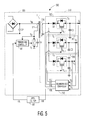
- FIG. 5 illustrates a circuit diagram of a soft-switching multiple-output flyback converter in accordance with the present invention.
- FIGS. 6A-6E illustrate idealized waveforms during a switching period of the soft-switched multiple-output flyback converter of FIG. 5 .
- Converter 500 includes a primary circuit 505 , a regulated output circuit 510 and an opto-coupler 520 .
- Optical coupler 520 operates to electrically isolate and optically couple feedback information from the regulated output circuit 510 .
- the primary circuit 505 includes a primary winding 514 of a transformer T coupled to a power switch S 0 , a rectified input voltage, V in and a primary-side controller 507 .
- a transformer current flows through the primary winding 514 and stores energy in the magnetic field of the transformer T.
- the power switch is non-conductive, the energy stored in the magnetic field is transferred to the secondary winding 516 to develop two or more DC output voltages.
- the regulated output circuit 510 coupled to the secondary winding 516 of the transformer T, includes three output channels in the exemplary embodiment.
- a first output channel 520 is coupled to the secondary winding 516 of the transformer T and to a first output V 1 .
- the first channel includes a diode D 1 , a switch S 1 and a capacitor C 1 .
- a second output channel 540 is coupled to the secondary winding 516 of the transformer T and to a second output V 2 .
- the second channel includes a diode D 2 , a switch S 2 and a capacitor C 2 .
- a third output channel 560 is coupled to the secondary winding 516 of the transformer T and to a third output V 3 .
- the third output includes a diode D 3 , a switch S 3 and a capacitor C 3 .
- Capacitors C 1 , C 2 and C 3 connect the respective outputs V 1 , V 2 and V 3 to the ground of the return line to stabilize the output voltages by absorbing high frequency ripple current.
- Diodes D 1 , D 2 and D 3 prevent current flow back into the secondary winding.
- each of switches S 1 , S 2 and S 3 comprise a MOSFET, the anti-parallel rectifier comprising a body diode of the MOSFET.
- BJTs bipolar junction transistors
- Drive control for switches S 1 , S 2 and S 3 is provided by a secondary-side controller 512 which receives as input, output voltages V 1 , V 2 and V 3 and processes the respective output signals to generate corresponding output error signals V 1E , V 2E and V 3E to drive pulse width modulation (PWM) circuitry in the secondary-side controller 512 to drives switches S 1 , S 2 and S 3 to maintain a regulated output voltage.
- PWM pulse width modulation
- the regulation scheme shown in FIG. 5 is commonly called secondary side regulation because switches are used on the secondary side of the transformer to regulate the output voltages.
- the power converter 500 further includes a primary-side controller 507 .
- the primary-side controller 507 performs two essential functions to effect zero-voltage switching of the primary side switch. First, the controller 507 monitors the drain voltage V d of transformer T to turn on the primary side switch at a voltage minimum of the drain voltage V d waveform. Second, at the point in time at which the primary side switch is turned on, the controller 507 utilizes the secondary side output error signal corresponding to the output channel sequenced last in the energy cycle to adjust the relative duty cycle of the primary side power switch S 0 .
- the output channels are sequenced in the following first to last order: output channel 520 , 540 and 560 . Accordingly, error signal V 3E corresponding to the third output channel 560 is continuously fed back from the secondary-side controller 512 , via the opto-coupler 520 , to the primary-side controller 507 to adjust the relative duty cycle of the power switch S 0 at a point in time when switch S 0 is turned on.
- circuit of the present invention could have a different number of output circuits than that shown in the exemplary circuit of FIG. 5 without altering the basic circuit principles and mode of operation.
- FIGS. 6 a-d illustrate the open and closed states of the switches ⁇ S 0 , S 1 , S 2 and S 3 ⁇ during the charge/discharge cycle and
- FIG. 6 e illustrates the drain voltage V d of the bottom of the primary side winding 514 of the transformer T for this time interval.
- the configuration of the switches S 0 , S 1 , S 2 and S 3 in the present invention determines whether the circuit is in the charge or discharge phase of the cycle.
- T charge (i.e., time period A to B)
- the rectified input voltage from the main power source, V in charges transformer T.
- All of the switches ⁇ S 1 , S 2 and S 3 ⁇ are in the open state, except for the switch S 0 (see FIG. 6 a ).
- the switch S 0 is opened at time B.
- the first switch in the switching sequence e.g., switch S 1
- switch S 1 is usually turned on somewhat ahead of the primary switch S 0 being turned off.
- T discharge of the energy cycle (i.e., time period B to E)
- only one switch is in a closed state at any given time (e.g., S 1 or S 2 or S 3 ⁇ so that the load coupled to the closed switch will receive the maximum charge from the transformer T.
- Each secondary side switch is closed for a time sufficient to perform voltage regulation.
- voltage regulation is performed on the secondary side utilizing the secondary controller 512 by coordinating and implementing the time duration for the open and closed states for the secondary side switches by feeding back an error signal from the secondary-side controller 512 to be applied to the gates of the secondary side switches.
- the secondary side control is not effected for the output channel to be sequenced last in each charge/discharge cycle. The last output channel is controlled from the primary side, as will be described. It is further noted that any of the output channels could be sequenced last in the energy cycle sequencing order.
- the switch S 1 remains closed (see FIG. 6 b ).
- the drain voltage (see FIG. 6 e ) due to the leakage inductance of the primary side.
- the drain voltage eventually settles down to a level equal to the sum of the input voltage plus the reflected voltage of voltage V 1 , the output of channel 520 . That is the drain voltage V d , equals (V rl +V IN ).
- the switch S 2 is in a closed state (see FIG. 6 c ) and the switch S 1 is in an open state (see FIG. 6 b ).
- the drain voltage V d is equal to the sum of the input voltage plus the reflected voltage of the second output channel voltage V 2 . That is, the drain voltage V d equals (V r2 +V IN ).
- the switch S 3 is in a closed state (see FIG. 6 d ) and the switch S 2 is in an open state (see FIG. 6 c ).
- the drain voltage V d is equal to the sum of the input voltage plus the reflected voltage of the third output channel voltage V 3 . That is, the drain voltage V d equals (V r3 +V IN ).
- Time period E marks the end of the demagnitization sub-phase T demag and the start of the resonance sub-phase T res . The significance of this demarcation will now be described.
- switch S 3 transitions from a closed to an open state.
- time period E which marks the demarcation point between the two sub-phases, discharge and resonance
- switch S 3 transitions from a closed to an open state.
- time period E occurs at a point in time at which the secondary-side current becomes substantially zero.
- the zero current condition occurs as a result of the transformer T becoming demagnetized, i.e., no stored energy is left in the transformer for the present energy cycle. Accordingly, at point E, there is no longer a reflected voltage on the primary side. This situation causes a resonance condition (see FIG. 6 e ) between capacitor C 5 and the magnetizing inductance of the primary winding 14 of transformer T 1 .
- the resonance condition is used to perform soft-switching of the primary-side switch.
- Soft-switching of the primary switch, S 0 is achieved via the primary controller 507 by detecting the resonance condition (see FIG. 6 e ) and determining one of the minima of the resonance to turn on switch S 0 .
- points B and C denote resonance minima.
- the amplitude of the resonant waveform of FIG. 6 e is determined by the magnitude of the reflected voltage of the last output to be switched in the energy cycle.
- the amplitude of the waveform of FIG. 6 e is determined by the reflected voltage, V r3 . It is further noted that if the reflected voltage (e.g., V r3 ) is large enough, the minima of the waveform can approach zero volts.
Abstract
A flyback power converter is described which provides multiple independently regulated outputs. Zero-volt primary side switching is achieved at a resonance minimum which occurs at the end of each energy cycle between a primary side capacitor and an isolation transformer primary winding.
Description
1. Technical Field of the Invention
The present invention relates in general, to power conversion and, more specifically, to a multiple output flyback converter, having improved cross-regulation and soft-switching to eliminate switching losses in the converter.
2. Description of the Related Art
Power converters are widely used to provide required voltages and load currents especially in environments that have higher concentrations of telecommunications or computer equipment. These power converters are often required to provide higher levels of output power for a small physical volume, since space is often at a premium. This requirement dictates that the power converters be high power density devices. These higher power density concentrations also dictate that the power converter operate with as high an efficiency as possible to minimize the converter's heat generation and therefore its operating temperature rise to the degree possible.
Through the use of switching regulator techniques, power converter efficiencies may be achieved that are typically higher than those of linear regulation techniques. These switching regulator techniques, however, give rise to other efficiency-decreasing problems that are not typically encountered in linear regulators. Because of higher switching frequencies (50 to 100 kilohertz), parasitic circuit inductance and capacitance elements in the transformers and switching devices cause “ringing” due to circuit resonances. This ringing typically presents both device and efficiency problems that must be addressed to operate the converters at high power densities.
One prior-art method for increasing power density of dc-to-dc converters, particularly in applications where more than one output voltage is required, is to use a single power stage with multiple windings on the power transformer, one for each output voltage. In such a converter, all outputs share the same inverter stage, and only one output, called the main output, is fully regulated by pulse-width modulation of the inverter switches on the primary side. Such a solution then requires feedback isolation, and additional post-regulators are required for independent regulation of the auxiliary outputs against load variation.
The flyback converter is a very popular power supply topology for use in low-power,multiple output applications. When the main output voltage regulation requirement is moderate, these converters may be operated with the main output being regulated by the switching regulator and the other output (s) being “cross-regulated”, i.e., the ratio of the output voltages on the different windings is determined by the winding ratio and the actual relative voltage levels are determined by the ‘on’ time of the main switch. Cross-regulation of each output voltage is achieved by the turns ratio of the secondary windings.
FIG. 1 illustrates a prior art flyback converter that uses a single switch on the primary side of the transformer to directly regulate one of the output voltage, i.e., Va, using feedback control. The cross-regulation of the other output voltages, i.e., Vb and Vc, is achieved by the turns ratio of the secondary winding. A drawback of the flyback converter of FIG. 1 is the presence of parasitics which result in wide tolerances for the cross-regulated outputs, which do not satisfy strict regulation requirements. Post-regulators (e.g., linear regulators) are sometimes used to improve the regulation of the output voltages. However, this approach increases cost and reduces efficiency of the power supply. A secondary side control method has been proposed as a solution to this shortcoming.
European patent No. 0 698 959 discloses one secondary-side control method which includes switches on the secondary-side of the transformer to provide independently regulated outputs. FIG. 2 illustrates a flyback converter where a rectifying diode is connected in series with each secondary winding. The corresponding regulator RS1 of the first output circuit controls the regulator (RS0) of the primary-side circuit. Output regulators RS2, RS3, control the secondary-side switches S2, S3 correspondingly. The input DC voltage Vin, a voltage representation of the primary-side switch S0 and one output of the regulators RS2, RS3 are also fed to the primary-side regulator RS0.
EP 0 772 284 discloses another secondary-side control method where one secondary winding supplies multiple output voltages via separate branches as shown in FIG. 3. Each output voltage is rectified by means of a diode. The first output V1 is regulated by the pulse width of the primary-sie switch S0. A switch is inserted into each branch supplying the rest of the output voltages (V2, V3). A regulator senses each of the output voltages V2, V3. The regulator controls the duty cycle of the corresponding switch to regulate the output voltage.
U.S. Pat. No. 5,617,015 to Goder et al., discloses a voltage regulator providing multiple independently regulated outputs. FIG. 4 illustrates a boost topology circuit configuration disclosed in Goder. However, it is disclosed that voltage-regulator may be implemented with a flyback or other topologies. A dedicated switch to each output voltage controls the energy delivery to the output. Energy is delivered to only those outputs that have fallen below the lower limit of an acceptable range. The voltage regulator will stop supplying the outputs that have exceeded the upper limit of an acceptable range.
European patents Nos. 0 698 959 and 0 772 284 and U.S. Pat. No. 5,617,015 to Goder each recite control of the on/off state of the primary-side switch based on the values of the output voltages. While each resolve the problem of primary side control of one of the outputs, they share a common drawback. Specifically, the secondary side control methods disclosed by each result in hard switching of the primary-side switch thus increasing switching losses and thereby reducing the efficiency of the power converter.
A further drawback associated with the circuits of FIG. 2 and 3 is that one of the output voltages has no secondary-side switch dedicated to its regulation. Instead, the output includes a rectifying diode and is regulated by the primary side switch. This is problematic in reduced power modes of operation (e.g., standby) where it is desirable to disable some of the outputs. This cannot be achieved with the circuit configurations of FIGS. 2 and 3 because the output which does not include the secondary-side switch cannot be disabled without disabling all of the outputs.
A still further drawback associated with the circuit of FIG. 4 is that the regulation method described therein increases the peak output current resulting in increased ripple compared with methods that continuously provide current to the multiple outputs.
In order to solve problems associated with parasitics which result in wide tolerances for the cross-regulated outputs, an objective of this invention is to make the converter insensitive to these parasitic effects by providing secondary-side control.
A related objective of the present invention is to enable soft-switching of the primary side switch by taking advantage of the method of secondary-side control.
To address the above-discussed deficiencies of the prior art, the present invention provides, a circuit which combines secondary-side regulation with primary-side zero-volt switching to achieve a level of circuit efficiency and flexibility not available in prior art circuit constructions.
The novel circuit provides circuit efficiency by providing zero-volt switching of the primary side switch. Zero-volt switching is achieved by taking advantage of a resonance which occurs between a switch capacitor coupled in parallel with a primary side power switch and a magnetization inductance of a primary side winding. A primary side controller detects the resonance condition and switches the power switch at one of the resonant waveform minima.
The novel circuit further provides flexibility via secondary-side regulation. In particular, the circuit provides means for independently and selectively disabling one or more output channels of the converter by providing a secondary side switch in each of a plurality of output circuits. An output circuit or channel can be selectively disabled, via the switch, by blocking the secondary winding current from flowing into the selected output.
In an embodiment to be illustrated and described, the isolation power converter is a flyback isolation converter including a power transformer, a power switch on the primary side and a secondary side including three output channels connected to a single secondary winding, where the first two output channels switched in each energy cycle are regulated on the secondary side and the last output channel to be switched in each energy cycle is controlled from the primary side. Primary-side control of the last output to be switched in the sequence is effected by an error signal which is transmitted from the secondary-side, via an opto-coupler, to a pulse-width modulator on the primary side for controlling the duty cycle of the power switch on the primary side. While separate voltage controlled switches are include in each output channel, the switch associated with the final output channel to be sequenced is subsidiary to the primary side power switch. However, separate switches are included in each output channel to selectively disable one or more of the output channels by blocking the secondary winding current from flowing into the disabled output(s).
The present invention introduces, in another aspect, a circuit capable of effecting substantially zero-volt switching of a power switch of the primary switching circuit in the primary side switch to increase the efficiency of the power converter.
In an embodiment to be illustrated and described, the primary and secondary side switches are metal oxide semiconductor field-effect transistor switches (MOSFETs). Those skilled in the pertinent art will understand, however, that the present invention fully encompasses all controllable switches, whether conventional or later-developed. An external diode may be employed as required to supplement the internal body diode of the clamping switch. Of course, an external diode may be employed if the clamping switch does not include a body diode.
In one embodiment of the present invention, the converter is selected from the group consisting of a flyback converter, a forward converter and a half-bridge converter. Those skilled in the pertinent art understand, however, that other isolated converter topologies are well within the broad scope of the present invention.
The foregoing features of the present invention will become more readily apparent and may be understood by referring to the following detailed description of an illustrative embodiment of the present invention, taken in conjunction with the accompanying drawings, where:
FIG. 1 is a circuit diagram illustrating a conventional flyback converter that uses a single switch on the primary side of the transformer to directly regulate one of the output voltages;
FIG. 2 is a circuit diagram illustrating a conventional flyback converter which illustrates one secondary-side control method according to the prior art;
FIG. 3 is a circuit diagram illustrating a conventional flyback converter which illustrates another secondary-side control method according to the prior art;
FIG.4 is a circuit diagram illustrating a dedicated switch in each output according to the prior art;
FIG. 5 illustrates a circuit diagram of a soft-switching multiple-output flyback converter in accordance with the present invention; and
FIGS. 6A-6E illustrate idealized waveforms during a switching period of the soft-switched multiple-output flyback converter of FIG. 5.
Referring to FIG. 5, a schematic diagram of an exemplary embodiment of the present flyback converter circuit is illustrated, and is generally identified by the numeral 500. Converter 500 includes a primary circuit 505, a regulated output circuit 510 and an opto-coupler 520. Optical coupler 520 operates to electrically isolate and optically couple feedback information from the regulated output circuit 510. The primary circuit 505, includes a primary winding 514 of a transformer T coupled to a power switch S0, a rectified input voltage, Vin and a primary-side controller 507. When the power switch S0 conducts, a transformer current flows through the primary winding 514 and stores energy in the magnetic field of the transformer T. When the power switch is non-conductive, the energy stored in the magnetic field is transferred to the secondary winding 516 to develop two or more DC output voltages.
The regulated output circuit 510, coupled to the secondary winding 516 of the transformer T, includes three output channels in the exemplary embodiment. A first output channel 520 is coupled to the secondary winding 516 of the transformer T and to a first output V1. The first channel includes a diode D1, a switch S1 and a capacitor C1. A second output channel 540 is coupled to the secondary winding 516 of the transformer T and to a second output V2. The second channel includes a diode D2, a switch S2 and a capacitor C2. A third output channel 560 is coupled to the secondary winding 516 of the transformer T and to a third output V3. The third output includes a diode D3, a switch S3 and a capacitor C3. Capacitors C1, C2 and C3 connect the respective outputs V1, V2 and V3 to the ground of the return line to stabilize the output voltages by absorbing high frequency ripple current. Diodes D1, D2 and D3 prevent current flow back into the secondary winding. Preferably, each of switches S1, S2 and S3 comprise a MOSFET, the anti-parallel rectifier comprising a body diode of the MOSFET. Of course, other types of switches, including bipolar junction transistors (BJTs), are well within the broad scope of the present invention.
Drive control for switches S1, S2 and S3 is provided by a secondary-side controller 512 which receives as input, output voltages V1, V2 and V3 and processes the respective output signals to generate corresponding output error signals V1E, V2E and V3E to drive pulse width modulation (PWM) circuitry in the secondary-side controller 512 to drives switches S1, S2 and S3 to maintain a regulated output voltage.
The regulation scheme shown in FIG. 5 is commonly called secondary side regulation because switches are used on the secondary side of the transformer to regulate the output voltages.
The power converter 500 further includes a primary-side controller 507. The primary-side controller 507 performs two essential functions to effect zero-voltage switching of the primary side switch. First, the controller 507 monitors the drain voltage Vd of transformer T to turn on the primary side switch at a voltage minimum of the drain voltage Vd waveform. Second, at the point in time at which the primary side switch is turned on, the controller 507 utilizes the secondary side output error signal corresponding to the output channel sequenced last in the energy cycle to adjust the relative duty cycle of the primary side power switch S0.
In the exemplary circuit of FIG. 5, the output channels are sequenced in the following first to last order: output channel 520, 540 and 560. Accordingly, error signal V3E corresponding to the third output channel 560 is continuously fed back from the secondary-side controller 512, via the opto-coupler 520, to the primary-side controller 507 to adjust the relative duty cycle of the power switch S0 at a point in time when switch S0 is turned on.
Further, it will be apparent to one of ordinary skill in the art that the circuit of the present invention could have a different number of output circuits than that shown in the exemplary circuit of FIG. 5 without altering the basic circuit principles and mode of operation.
Circuit Operation
Operation of the inventive circuit 500 of FIG. 5 may be more readily understood with reference to the idealized switching circuit waveforms of FIG. 6 for one charge/discharge cycle as defined by the time interval A to F. FIGS. 6a-d illustrate the open and closed states of the switches {S0, S1, S2 and S3} during the charge/discharge cycle and FIG. 6e illustrates the drain voltage Vd of the bottom of the primary side winding 514 of the transformer T for this time interval. The configuration of the switches S0, S1, S2 and S3, in the present invention determines whether the circuit is in the charge or discharge phase of the cycle.
Charging Phase
During the charge phase of the cycle, Tcharge, (i.e., time period A to B), the rectified input voltage from the main power source, Vin, charges transformer T. All of the switches {S1, S2 and S3} are in the open state, except for the switch S0 (see FIG. 6a). Once the transformer T is sufficiently charged, the switch S0 is opened at time B. In actual operation, the first switch in the switching sequence, e.g., switch S1, is usually turned on somewhat ahead of the primary switch S0 being turned off. In general, there may often be some overlap between the ‘on’ and ‘off’ times off the sequential controlled switches. This occurs for two reasons, first, the flyback converter should not be left “unloaded”, and secondly, soft-switching can sometimes be achieved with some overlap.
Discharge Phase
During the discharge phase, Tdischarge, of the energy cycle (i.e., time period B to E), only one switch is in a closed state at any given time (e.g., S1 or S2 or S3} so that the load coupled to the closed switch will receive the maximum charge from the transformer T. Each secondary side switch is closed for a time sufficient to perform voltage regulation. Specifically, voltage regulation is performed on the secondary side utilizing the secondary controller 512 by coordinating and implementing the time duration for the open and closed states for the secondary side switches by feeding back an error signal from the secondary-side controller 512 to be applied to the gates of the secondary side switches. It is noted, however, that the secondary side control is not effected for the output channel to be sequenced last in each charge/discharge cycle. The last output channel is controlled from the primary side, as will be described. It is further noted that any of the output channels could be sequenced last in the energy cycle sequencing order.
The discharge phase of the energy cycle is now described in detail.
For the time period B to C, the switch S1 remains closed (see FIG. 6b). Initially, at time period B, there is an overshoot in the drain voltage (see FIG. 6e) due to the leakage inductance of the primary side. The drain voltage eventually settles down to a level equal to the sum of the input voltage plus the reflected voltage of voltage V1, the output of channel 520. That is the drain voltage Vd, equals (Vrl+VIN).
For the time period C to D, the switch S2 is in a closed state (see FIG. 6c) and the switch S1 is in an open state (see FIG. 6b). During this time, the drain voltage Vd is equal to the sum of the input voltage plus the reflected voltage of the second output channel voltage V2. That is, the drain voltage Vd equals (Vr2+VIN).
For the time period D to E, the switch S3 is in a closed state (see FIG. 6d) and the switch S2 is in an open state (see FIG. 6c). During this time, the drain voltage Vd is equal to the sum of the input voltage plus the reflected voltage of the third output channel voltage V3. That is, the drain voltage Vd equals (Vr3+VIN).
Time period E marks the end of the demagnitization sub-phase Tdemag and the start of the resonance sub-phase Tres. The significance of this demarcation will now be described.
At time period E, which marks the demarcation point between the two sub-phases, discharge and resonance, switch S3 transitions from a closed to an open state. At time period E occurs at a point in time at which the secondary-side current becomes substantially zero. One way of determining a substantially zero secondary-side current is with a monitoring circuit. The zero current condition occurs as a result of the transformer T becoming demagnetized, i.e., no stored energy is left in the transformer for the present energy cycle. Accordingly, at point E, there is no longer a reflected voltage on the primary side. This situation causes a resonance condition (see FIG. 6e) between capacitor C5 and the magnetizing inductance of the primary winding 14 of transformer T1. The resonance condition is used to perform soft-switching of the primary-side switch. Soft-switching of the primary switch, S0, is achieved via the primary controller 507 by detecting the resonance condition (see FIG. 6e) and determining one of the minima of the resonance to turn on switch S0. Referring to FIG. 6e, points B and C denote resonance minima.
It is further noted that the amplitude of the resonant waveform of FIG. 6e is determined by the magnitude of the reflected voltage of the last output to be switched in the energy cycle. In the illustrative circuit, the amplitude of the waveform of FIG. 6e is determined by the reflected voltage, Vr3. It is further noted that if the reflected voltage (e.g., Vr3) is large enough, the minima of the waveform can approach zero volts.
Although the invention has been described with a certain degree of particularity, various modifications may be made to the embodiments disclosed herein. It is, therefore, to be understood that the above description should not be construed as limiting, but merely as an exemplification of the various embodiments.
Claims (5)
1. A flyback power converter comprising a primary side and a secondary side:
said primary side comprising:
a power switch and a primary winding of a power transformer connected in a series combination, the series combination connected in parallel across first and second input supply nodes;
an input capacitor connected in parallel across the first and second input supply nodes; and
a switch capacitor connected in parallel across said power switch; said secondary side comprising:
a secondary winding of the power transformer connected in parallel across a first and a secondary side node;
multiple output circuits wherein each of said multiple output circuits include a rectifier, a switch and an output capacitor wherein said rectifier is connected in series between the first secondary side node and said switch, and said output capacitor is connected in parallel across a first output node;
means for performing secondary-side regulation of at least one output from said multiple output circuits; and
wherein a zero voltage switching condition of said power switch occurs at a resonance minimum of a resonant condition between said primary side winding and said switch capacitor.
2. The flyback converter of claim 1 , further comprising a primary side controller operable to detect said resonance minimum and cause the power switch to be turned on when the voltage across the power switch is substantially equal to zero volts.
3. The flyback converter of claim 2 , wherein said primary controller includes a first input for receiving a drain voltage of said primary side winding to detect said resonance condition.
4. The flyback converter of claim 3 , wherein said primary controller further includes a second input for receiving a secondary side signal for controlling a duty cycle of said power switch.
5. The flyback converter of claim 1 , wherein the power switch is selected from the group consisting of a FET device, an insulated gate bipolar transistor device.
Priority Applications (9)
| Application Number | Priority Date | Filing Date | Title |
|---|---|---|---|
| US10/017,346 US6504267B1 (en) | 2001-12-14 | 2001-12-14 | Flyback power converter with secondary-side control and primary-side soft switching |
| JP2003553696A JP2005513984A (en) | 2001-12-14 | 2002-12-03 | Flyback power converter |
| DE60207110T DE60207110D1 (en) | 2001-12-14 | 2002-12-03 | LOCK POWER CONVERTER |
| AU2002351107A AU2002351107A1 (en) | 2001-12-14 | 2002-12-03 | Flyback power converter |
| CNA028248724A CN1602579A (en) | 2001-12-14 | 2002-12-03 | Flyback power converter |
| KR10-2004-7009224A KR20040068239A (en) | 2001-12-14 | 2002-12-03 | Flyback Power Converter |
| AT02785820T ATE308818T1 (en) | 2001-12-14 | 2002-12-03 | BLOCK POWER CONVERTER |
| PCT/IB2002/005124 WO2003052913A1 (en) | 2001-12-14 | 2002-12-03 | Flyback power converter |
| EP02785820A EP1459431B1 (en) | 2001-12-14 | 2002-12-03 | Flyback power converter |
Applications Claiming Priority (1)
| Application Number | Priority Date | Filing Date | Title |
|---|---|---|---|
| US10/017,346 US6504267B1 (en) | 2001-12-14 | 2001-12-14 | Flyback power converter with secondary-side control and primary-side soft switching |
Publications (1)
| Publication Number | Publication Date |
|---|---|
| US6504267B1 true US6504267B1 (en) | 2003-01-07 |
Family
ID=21782059
Family Applications (1)
| Application Number | Title | Priority Date | Filing Date |
|---|---|---|---|
| US10/017,346 Expired - Fee Related US6504267B1 (en) | 2001-12-14 | 2001-12-14 | Flyback power converter with secondary-side control and primary-side soft switching |
Country Status (9)
| Country | Link |
|---|---|
| US (1) | US6504267B1 (en) |
| EP (1) | EP1459431B1 (en) |
| JP (1) | JP2005513984A (en) |
| KR (1) | KR20040068239A (en) |
| CN (1) | CN1602579A (en) |
| AT (1) | ATE308818T1 (en) |
| AU (1) | AU2002351107A1 (en) |
| DE (1) | DE60207110D1 (en) |
| WO (1) | WO2003052913A1 (en) |
Cited By (77)
| Publication number | Priority date | Publication date | Assignee | Title |
|---|---|---|---|---|
| US20040150264A1 (en) * | 2002-11-06 | 2004-08-05 | Kazuyuki Kudo | Electric power supply unit and electric power supply controlling method |
| US20040239512A1 (en) * | 2003-05-30 | 2004-12-02 | Adc Dsl Systems, Inc. | Lightning protection for a network element |
| US20040239513A1 (en) * | 2003-05-30 | 2004-12-02 | Adc Dsl Systems, Inc. | Input voltage sense circuit in a line powered network element |
| US20050035662A1 (en) * | 2003-07-11 | 2005-02-17 | Stowell John R. | Reduced component power converter with independent regulated outputs and method |
| US20050088858A1 (en) * | 2002-02-23 | 2005-04-28 | Reinhard Kogel | Power supply unit comprising a switched-mode power supply |
| US20060007617A1 (en) * | 2004-06-29 | 2006-01-12 | Christian Kranz | DC voltage converter and method for converting a DC voltage |
| US20060119185A1 (en) * | 2004-12-07 | 2006-06-08 | Steigerwald Robert L | Soft switched secondary side post regulator for DC to DC converter |
| US20060145676A1 (en) * | 2003-08-15 | 2006-07-06 | Atmel Germany Gmbh | Method and circuit arrangement for a power supply |
| US20060158908A1 (en) * | 2005-01-14 | 2006-07-20 | Sanken Electric Co., Ltd. | DC-DC converter of multi-output type |
| US20060209572A1 (en) * | 1997-01-24 | 2006-09-21 | Schlecht Martin F | High efficiency power converter |
| US20060221647A1 (en) * | 2005-04-01 | 2006-10-05 | Harmer+Simmons(France)Sas | Converter having a plurality of channels |
| US20060262575A1 (en) * | 1997-01-24 | 2006-11-23 | Schlecht Martin F | Power converter with isolated and regulation stages |
| US20070159421A1 (en) * | 2006-01-10 | 2007-07-12 | Powerdsine, Ltd. | Secondary Side Post Regulation for LED Backlighting |
| US20070217101A1 (en) * | 2006-03-17 | 2007-09-20 | Adc Dsl Systems, Inc. | Auto-resetting span-power protection |
| US20080151582A1 (en) * | 1997-01-24 | 2008-06-26 | Schlecht Martin F | High efficiency power converter |
| US20080157597A1 (en) * | 2006-12-27 | 2008-07-03 | Annabelle Pratt | Multiple output isolated converter circuit |
| US20080211304A1 (en) * | 2006-11-01 | 2008-09-04 | Synqor, Inc. | Intermediate bus architecture with a quasi-regulated bus converter |
| US20090179491A1 (en) * | 2008-01-15 | 2009-07-16 | Microsemi Corporation | Fine tuned multiple output converter |
| US20090257580A1 (en) * | 2002-04-29 | 2009-10-15 | Adc Dsl Systems, Inc. | Function for controlling line powered network element |
| US20110002146A1 (en) * | 2007-08-27 | 2011-01-06 | Sanken Electric Co., Ltd. | Multiple output switching power source apparatus |
| US20110007534A1 (en) * | 2009-07-10 | 2011-01-13 | Regents Of The University Of Minnesota | Soft switching power electronic transformer |
| US20110012542A1 (en) * | 2009-07-20 | 2011-01-20 | Denso Corporation | Drive system for power switching elements |
| US20110032731A1 (en) * | 2009-08-04 | 2011-02-10 | Asic Advantage Inc. | Multiple independently regulated parameters using a single magnetic circuit element |
| CN102017381A (en) * | 2008-04-25 | 2011-04-13 | 动力研究电子股份有限公司 | Power converter |
| WO2011100861A1 (en) * | 2010-02-22 | 2011-08-25 | Telefonaktiebolaget L M Ericsson (Publ) | Power conversion circuit and method of power conversion |
| US8154894B1 (en) * | 2005-10-13 | 2012-04-10 | ERP Power, LLC | Multiple voltage DC to DC resonant converter |
| US20120134181A1 (en) * | 2010-11-30 | 2012-05-31 | Fuji Electric Co., Ltd. | Gate driving power supply system and inverter control circuit |
| EP2341761A3 (en) * | 2007-06-15 | 2012-09-26 | Tridonic GmbH & Co KG | Apparatus for operating a light source, in particular LED |
| US20120267953A1 (en) * | 2011-04-19 | 2012-10-25 | Doyle Kevin A | Apparatus and method for controlling and supplying power to electrical devices in high risk environments |
| DE102012000683A1 (en) * | 2012-01-17 | 2013-07-18 | Phoenix Contact Gmbh & Co. Kg | Multi-channel controlled DC / DC converter for redundant power supply in safety technology |
| US20140092651A1 (en) * | 2012-10-03 | 2014-04-03 | Belenos Clean Power Holding Ag | Micro-inverter with improved control |
| US20140232181A1 (en) * | 2011-09-27 | 2014-08-21 | Hitachi Automotive Systems, Ltd | Automotive Vehicle Inverter Control Apparatus |
| CN104270009A (en) * | 2014-09-23 | 2015-01-07 | 广东美的制冷设备有限公司 | Multi-output power circuit and air conditioner |
| EP2775602A3 (en) * | 2013-03-08 | 2015-04-08 | Power Integrations, Inc. | Techniques for controlling a power converter using multiple controllers |
| US20150131333A1 (en) * | 2011-12-09 | 2015-05-14 | Telefonaktiebolaget L M Ericsson (Publ) | Dc-dc converter with multiple outputs |
| EP2544352A3 (en) * | 2011-07-08 | 2015-06-10 | Vestel Elektronik Sanayi ve Ticaret A.S. | Momentary power interruption and voltage dips reset protection |
| EP2342947B1 (en) | 2008-11-05 | 2015-07-08 | Tridonic GmbH & Co KG | Illuminant operating appliance with potential separation |
| TWI497892B (en) * | 2012-07-13 | 2015-08-21 | Tpv Electronics Fujian Co Ltd | Liquid crystal display products and its flyback power conversion device |
| US20150364984A1 (en) * | 2014-06-12 | 2015-12-17 | Denso Corporation | Power supply apparatus for power converters |
| EP2996236A1 (en) | 2014-09-09 | 2016-03-16 | Valeo Equipements Electriques Moteur | Method for adjusting a dc switching-mode power supply with a transformer having multiple output voltages, corresponding power supply and use |
| WO2016045052A1 (en) * | 2014-09-25 | 2016-03-31 | Intel Corporation | Power supply unit adaptable for various power modes |
| US20160149504A1 (en) * | 2014-11-20 | 2016-05-26 | Microchip Technology Incorporated | Start-up controller for a power converter |
| US9491815B2 (en) | 2013-10-02 | 2016-11-08 | Microsemi Corporation | LED luminaire driving circuit and method |
| US9548662B2 (en) | 2010-12-02 | 2017-01-17 | Murata Manufacturing Co., Ltd. | Switching power-supply circuit |
| US20170033698A1 (en) * | 2015-07-31 | 2017-02-02 | Texas Instruments Incorporated | Flyback converter with secondary side regulation |
| US9621048B2 (en) | 2010-12-02 | 2017-04-11 | Murata Manufacturing Co., Ltd. | Switching power-supply circuit |
| US9621021B2 (en) | 2013-06-21 | 2017-04-11 | Microchip Technology Inc. | Auxiliary power supplies in parallel with a switch of a switching regulator |
| US9705408B2 (en) | 2015-08-21 | 2017-07-11 | Microchip Technology Incorporated | Power converter with sleep/wake mode |
| EP3231255A4 (en) * | 2014-12-12 | 2017-12-20 | Switchtech AN | Driving circuitry for a lighting arrangement |
| TWI616059B (en) * | 2016-07-01 | 2018-02-21 | 瑞昱半導體股份有限公司 | Operation voltage testing circuit and method |
| US9912243B2 (en) | 2015-06-01 | 2018-03-06 | Microchip Technology Incorporated | Reducing power in a power converter when in a standby mode |
| US20180159434A1 (en) * | 2016-12-01 | 2018-06-07 | Power Integrations, Inc. | Controller for multi-output single magnetic component converter with independent regulation of constant current and constant voltage outputs |
| USRE47031E1 (en) | 2012-07-03 | 2018-09-04 | Cognipower, Llc | Power converter with demand pulse isolation |
| US10141830B1 (en) | 2017-10-31 | 2018-11-27 | Semiconductor Components Industries, Llc | Burst operation of a switching controller having a plurality of foldback curves |
| US10199950B1 (en) | 2013-07-02 | 2019-02-05 | Vlt, Inc. | Power distribution architecture with series-connected bus converter |
| US10277130B2 (en) | 2015-06-01 | 2019-04-30 | Microchip Technolgoy Incorporated | Primary-side start-up method and circuit arrangement for a series-parallel resonant power converter |
| US10320301B2 (en) | 2017-09-15 | 2019-06-11 | Semiconductor Components Industries, Llc | Power converter responsive to device connection status |
| US10326371B2 (en) | 2017-08-23 | 2019-06-18 | Semiconductor Components Industries, Llc | Providing adaptive output power |
| US10554206B2 (en) | 2018-02-27 | 2020-02-04 | Cognipower, Llc | Trigger circuitry for fast, low-power state transitions |
| US10554140B1 (en) | 2019-06-26 | 2020-02-04 | Cypress Semiconductor Corporation | AC-DC converter with secondary side-control and synchronous rectifier sense architecture |
| US10566904B2 (en) | 2017-10-16 | 2020-02-18 | Texas Instruments Incorporated | Multimode PWM converter with smooth mode transition |
| CN111082667A (en) * | 2020-01-22 | 2020-04-28 | Msj系统有限责任公司 | Multi-output switching power supply |
| US10651754B1 (en) | 2019-06-26 | 2020-05-12 | Cypress Semiconductor Corporation | Accurate peak detection architecture for secondary controlled AC-DC converter |
| US10651753B1 (en) * | 2019-06-26 | 2020-05-12 | Cypress Semiconductor Corporation | Accurate valley detection for secondary controlled flyback converter |
| US10693384B1 (en) * | 2019-06-26 | 2020-06-23 | Cypress Semiconductor Corporation | Accurate feed-forward sensing in flyback-transformer based secondary controller |
| US10784784B2 (en) | 2017-05-23 | 2020-09-22 | Semiconductor Components Industries, Llc | DC-DC converter with dynamic feedback loop |
| US10892755B2 (en) | 2018-02-27 | 2021-01-12 | Cognipower, Llc | Driver circuitry for fast, efficient state transitions |
| US11108331B2 (en) * | 2019-03-29 | 2021-08-31 | Power Integrations, Inc. | Method and apparatus for continuous conduction mode operation of a multi-output power converter |
| US20210298152A1 (en) * | 2018-07-13 | 2021-09-23 | 10644137 Canada Inc. | Apparatus and methods for high power led lights |
| CN113497568A (en) * | 2020-04-03 | 2021-10-12 | 台达电子企业管理(上海)有限公司 | Power adapter |
| US20210391802A1 (en) * | 2018-12-18 | 2021-12-16 | Mitsubishi Electric Corporation | Dc-dc converter |
| US11211870B2 (en) * | 2018-05-31 | 2021-12-28 | Power Integrations, Inc. | Method and apparatus for sequencing outputs in a multi-output power converter system |
| US20220029543A1 (en) * | 2018-12-03 | 2022-01-27 | Thyssenkrupp Presta Ag | Flyback converter having two or more independent output stages |
| US11496060B2 (en) | 2020-11-18 | 2022-11-08 | Power Integrations, Inc. | Pulse sharing control for enhancing performance in a multiple output power converter system |
| US11616449B2 (en) | 2020-04-03 | 2023-03-28 | Delta Electronics (Shanghai) Co., Ltd | Power adapter |
| US11711017B2 (en) | 2020-04-03 | 2023-07-25 | Delta Electronics (Shanghai) Co., Ltd | Adapter and control method thereof |
| US11737219B2 (en) | 2020-04-03 | 2023-08-22 | Delta Electronics (Shanghai) Co., Ltd | Power adapter |
Families Citing this family (11)
| Publication number | Priority date | Publication date | Assignee | Title |
|---|---|---|---|---|
| KR100791717B1 (en) | 2004-12-08 | 2008-01-03 | 산켄덴키 가부시키가이샤 | Dc-dc converter of multi-output type |
| KR100741471B1 (en) | 2006-09-29 | 2007-07-20 | 삼성전자주식회사 | Latch-free boosting scheme |
| KR100844874B1 (en) | 2006-12-27 | 2008-07-09 | 삼성전자주식회사 | Voltage generator for generating a plurality of boosting voltages and liquid crytal display having the same |
| DE102008052587A1 (en) | 2008-10-10 | 2010-04-15 | Isle Gmbh | Circuit arrangement for magnetic resonance coupling of multiple direct current circuits, has multiple coils of magnetic transformer connected with direct current circuit by resonance capacitor, resonance inductance and power converter unit |
| JP5353374B2 (en) * | 2009-03-31 | 2013-11-27 | パナソニック株式会社 | Time-sharing control power supply |
| JP2015177650A (en) * | 2014-03-14 | 2015-10-05 | 株式会社東芝 | power supply circuit |
| FR3037742B1 (en) * | 2015-06-16 | 2018-12-14 | Chauvin Arnoux | VERY LARGE DYNAMIC DECOUPING POWER SUPPLY FOR MEASURING INSTRUMENTS |
| TWI560539B (en) * | 2016-02-02 | 2016-12-01 | Asian Power Devices Inc | Dual power supply apparatus and method thereof |
| CN109660125A (en) * | 2017-10-12 | 2019-04-19 | 首利实业股份有限公司 | The circuit structure of high power power power supply unit |
| KR102545731B1 (en) * | 2018-11-02 | 2023-06-19 | 한국전기연구원 | Apparatus for generating waveform |
| CN115118174A (en) * | 2021-03-09 | 2022-09-27 | 华为数字能源技术有限公司 | Asymmetric half-bridge flyback converter and power supply system |
Citations (4)
| Publication number | Priority date | Publication date | Assignee | Title |
|---|---|---|---|---|
| EP0698959A1 (en) | 1994-08-22 | 1996-02-28 | Siemens Aktiengesellschaft Österreich | Flyback converter circuit |
| US5617015A (en) | 1995-06-07 | 1997-04-01 | Linear Technology Corporation | Multiple output regulator with time sequencing |
| EP0772284A2 (en) | 1995-10-31 | 1997-05-07 | KE KOMMUNIKATIONS-ELEKTRONIK GMBH & CO | Circuit arrangement generating DC voltages of different magnitudes |
| US6339262B1 (en) * | 1997-12-03 | 2002-01-15 | Fuji Electric Co., Ltd. | Switching power supply using an input DC power supply |
Family Cites Families (1)
| Publication number | Priority date | Publication date | Assignee | Title |
|---|---|---|---|---|
| JP3458370B2 (en) * | 1995-11-15 | 2003-10-20 | 横河電機株式会社 | Resonant converter |
-
2001
- 2001-12-14 US US10/017,346 patent/US6504267B1/en not_active Expired - Fee Related
-
2002
- 2002-12-03 JP JP2003553696A patent/JP2005513984A/en active Pending
- 2002-12-03 KR KR10-2004-7009224A patent/KR20040068239A/en not_active Application Discontinuation
- 2002-12-03 CN CNA028248724A patent/CN1602579A/en active Pending
- 2002-12-03 WO PCT/IB2002/005124 patent/WO2003052913A1/en active IP Right Grant
- 2002-12-03 EP EP02785820A patent/EP1459431B1/en not_active Expired - Lifetime
- 2002-12-03 AT AT02785820T patent/ATE308818T1/en not_active IP Right Cessation
- 2002-12-03 DE DE60207110T patent/DE60207110D1/en not_active Expired - Lifetime
- 2002-12-03 AU AU2002351107A patent/AU2002351107A1/en not_active Abandoned
Patent Citations (4)
| Publication number | Priority date | Publication date | Assignee | Title |
|---|---|---|---|---|
| EP0698959A1 (en) | 1994-08-22 | 1996-02-28 | Siemens Aktiengesellschaft Österreich | Flyback converter circuit |
| US5617015A (en) | 1995-06-07 | 1997-04-01 | Linear Technology Corporation | Multiple output regulator with time sequencing |
| EP0772284A2 (en) | 1995-10-31 | 1997-05-07 | KE KOMMUNIKATIONS-ELEKTRONIK GMBH & CO | Circuit arrangement generating DC voltages of different magnitudes |
| US6339262B1 (en) * | 1997-12-03 | 2002-01-15 | Fuji Electric Co., Ltd. | Switching power supply using an input DC power supply |
Cited By (155)
| Publication number | Priority date | Publication date | Assignee | Title |
|---|---|---|---|---|
| US20060209572A1 (en) * | 1997-01-24 | 2006-09-21 | Schlecht Martin F | High efficiency power converter |
| US7272023B2 (en) * | 1997-01-24 | 2007-09-18 | Synqor, Inc. | High efficiency power converter |
| US7272021B2 (en) | 1997-01-24 | 2007-09-18 | Synqor, Inc. | Power converter with isolated and regulated stages |
| US20080151582A1 (en) * | 1997-01-24 | 2008-06-26 | Schlecht Martin F | High efficiency power converter |
| US8023290B2 (en) | 1997-01-24 | 2011-09-20 | Synqor, Inc. | High efficiency power converter |
| US20080151580A1 (en) * | 1997-01-24 | 2008-06-26 | Schlecht Martin F | High efficiency power converter |
| US9143042B2 (en) | 1997-01-24 | 2015-09-22 | Synqor, Inc. | High efficiency power converter |
| US20060262575A1 (en) * | 1997-01-24 | 2006-11-23 | Schlecht Martin F | Power converter with isolated and regulation stages |
| US8493751B2 (en) | 1997-01-24 | 2013-07-23 | Synqor, Inc. | High efficiency power converter |
| US20110176333A1 (en) * | 1997-01-24 | 2011-07-21 | Synqor, Inc. | Power Converter with Isolated and Regulation Stages |
| US20080175024A1 (en) * | 1997-01-24 | 2008-07-24 | Schlecht Martin F | Power converter with isolated and regulation stages |
| US20050088858A1 (en) * | 2002-02-23 | 2005-04-28 | Reinhard Kogel | Power supply unit comprising a switched-mode power supply |
| US8073134B2 (en) | 2002-04-29 | 2011-12-06 | Adc Dsl Systems, Inc. | Function for controlling line powered network element |
| US20090257580A1 (en) * | 2002-04-29 | 2009-10-15 | Adc Dsl Systems, Inc. | Function for controlling line powered network element |
| US7239046B2 (en) * | 2002-11-06 | 2007-07-03 | Pioneer Corporation | Electric power supply unit and electric power supply controlling method |
| US20040150264A1 (en) * | 2002-11-06 | 2004-08-05 | Kazuyuki Kudo | Electric power supply unit and electric power supply controlling method |
| US20050254269A1 (en) * | 2003-05-30 | 2005-11-17 | Lomax Charles W Jr | Input voltage sense circuit in a line powered network element |
| CN1833262B (en) * | 2003-05-30 | 2012-03-28 | Adcdsl系统公司 | Input voltage sense circuit in a line powered network element |
| WO2004110077A3 (en) * | 2003-05-30 | 2005-12-15 | Adc Dsl Sys Inc | Input voltage sense circuit in a line powered network element |
| US6967585B2 (en) * | 2003-05-30 | 2005-11-22 | Adc Dsl Systems, Inc. | Input voltage sense circuit in a line powered network element |
| US20040239513A1 (en) * | 2003-05-30 | 2004-12-02 | Adc Dsl Systems, Inc. | Input voltage sense circuit in a line powered network element |
| US20040239512A1 (en) * | 2003-05-30 | 2004-12-02 | Adc Dsl Systems, Inc. | Lightning protection for a network element |
| US7233083B2 (en) * | 2003-07-11 | 2007-06-19 | Raytheon Company | Reduced component power converter with independent regulated outputs and method |
| US20050035662A1 (en) * | 2003-07-11 | 2005-02-17 | Stowell John R. | Reduced component power converter with independent regulated outputs and method |
| US20060145676A1 (en) * | 2003-08-15 | 2006-07-06 | Atmel Germany Gmbh | Method and circuit arrangement for a power supply |
| US7176661B2 (en) * | 2004-06-29 | 2007-02-13 | Infineon Technologies Ag | DC voltage converter and method for converting a DC voltage |
| US20060007617A1 (en) * | 2004-06-29 | 2006-01-12 | Christian Kranz | DC voltage converter and method for converting a DC voltage |
| US7400061B2 (en) * | 2004-12-07 | 2008-07-15 | Lockheed Martin Corporation | Soft switched secondary side post regulator for DC to DC converter |
| US20060119185A1 (en) * | 2004-12-07 | 2006-06-08 | Steigerwald Robert L | Soft switched secondary side post regulator for DC to DC converter |
| US7304867B2 (en) * | 2005-01-14 | 2007-12-04 | Sanken Electric Co., Ltd. | DC-DC converter of multi-output type |
| US20060158908A1 (en) * | 2005-01-14 | 2006-07-20 | Sanken Electric Co., Ltd. | DC-DC converter of multi-output type |
| US20060221647A1 (en) * | 2005-04-01 | 2006-10-05 | Harmer+Simmons(France)Sas | Converter having a plurality of channels |
| US7586761B2 (en) * | 2005-04-01 | 2009-09-08 | Harmer-Simmons (France)Sas | Converter having a plurality of channels |
| US8154894B1 (en) * | 2005-10-13 | 2012-04-10 | ERP Power, LLC | Multiple voltage DC to DC resonant converter |
| US20070159421A1 (en) * | 2006-01-10 | 2007-07-12 | Powerdsine, Ltd. | Secondary Side Post Regulation for LED Backlighting |
| US7923943B2 (en) | 2006-01-10 | 2011-04-12 | Microsemi Corp.—Analog Mixed Signal Group Ltd. | Secondary side post regulation for LED backlighting |
| US20070217101A1 (en) * | 2006-03-17 | 2007-09-20 | Adc Dsl Systems, Inc. | Auto-resetting span-power protection |
| US7433165B2 (en) | 2006-03-17 | 2008-10-07 | Adc Dsl Systems, Inc. | Auto-resetting span-power protection |
| US8149597B2 (en) | 2006-11-01 | 2012-04-03 | Synqor, Inc. | Intermediate bus architecture with a quasi-regulated bus converter |
| US20080211304A1 (en) * | 2006-11-01 | 2008-09-04 | Synqor, Inc. | Intermediate bus architecture with a quasi-regulated bus converter |
| US7787261B2 (en) | 2006-11-01 | 2010-08-31 | Synqor, Inc. | Intermediate bus architecture with a quasi-regulated bus converter |
| US20110187191A1 (en) * | 2006-11-01 | 2011-08-04 | Farrington Richard W | Intermediate Bus Architecture with a Quasi-Regulated Bus Converter |
| US20080157597A1 (en) * | 2006-12-27 | 2008-07-03 | Annabelle Pratt | Multiple output isolated converter circuit |
| AT515913B1 (en) * | 2007-06-15 | 2016-01-15 | Tridonic Gmbh & Co Kg | OPERATING DEVICE FOR OPERATING A LIGHT SOURCE, ESPECIALLY LED |
| EP2341761A3 (en) * | 2007-06-15 | 2012-09-26 | Tridonic GmbH & Co KG | Apparatus for operating a light source, in particular LED |
| AT515913A5 (en) * | 2007-06-15 | 2016-01-15 | Tridonic Gmbh & Co Kg | OPERATING DEVICE FOR OPERATING A LIGHT SOURCE, ESPECIALLY LED |
| EP2247162B1 (en) * | 2007-06-15 | 2016-01-06 | Tridonic GmbH & Co KG | Apparatus for operating a light source, in particular LED |
| US8189355B2 (en) * | 2007-08-27 | 2012-05-29 | Sanken Electric Co., Ltd. | Multiple output switching power source apparatus |
| US20110002146A1 (en) * | 2007-08-27 | 2011-01-06 | Sanken Electric Co., Ltd. | Multiple output switching power source apparatus |
| US7906868B2 (en) | 2008-01-15 | 2011-03-15 | Microsemi Corporation | Fine tuned multiple output converter |
| US20090179491A1 (en) * | 2008-01-15 | 2009-07-16 | Microsemi Corporation | Fine tuned multiple output converter |
| TWI458237B (en) * | 2008-01-15 | 2014-10-21 | Microsemi Corp | Multiple output flyback converter, and method of, and controller for, regulating output voltages thereof |
| CN102017381A (en) * | 2008-04-25 | 2011-04-13 | 动力研究电子股份有限公司 | Power converter |
| US20110260535A1 (en) * | 2008-04-25 | 2011-10-27 | Power Research Electronics B.V. | Power Converter |
| US8633613B2 (en) * | 2008-04-25 | 2014-01-21 | Power Research Electronics B.V. | Power converter |
| EP2342947B1 (en) | 2008-11-05 | 2015-07-08 | Tridonic GmbH & Co KG | Illuminant operating appliance with potential separation |
| AT518879A5 (en) * | 2008-11-05 | 2018-02-15 | Tridonic Gmbh & Co Kg | BULB OPERATOR WITH POTENTIAL SEPARATION |
| AT518879B1 (en) * | 2008-11-05 | 2018-02-15 | Tridonic Gmbh & Co Kg | BULB OPERATOR WITH POTENTIAL SEPARATION |
| US8446743B2 (en) * | 2009-07-10 | 2013-05-21 | Regents Of The University Of Minnesota | Soft switching power electronic transformer |
| US20110007534A1 (en) * | 2009-07-10 | 2011-01-13 | Regents Of The University Of Minnesota | Soft switching power electronic transformer |
| US20110012542A1 (en) * | 2009-07-20 | 2011-01-20 | Denso Corporation | Drive system for power switching elements |
| US8284575B2 (en) * | 2009-07-20 | 2012-10-09 | Denso Corporation | Drive system for power switching elements |
| US20110032731A1 (en) * | 2009-08-04 | 2011-02-10 | Asic Advantage Inc. | Multiple independently regulated parameters using a single magnetic circuit element |
| WO2011100861A1 (en) * | 2010-02-22 | 2011-08-25 | Telefonaktiebolaget L M Ericsson (Publ) | Power conversion circuit and method of power conversion |
| US20120134181A1 (en) * | 2010-11-30 | 2012-05-31 | Fuji Electric Co., Ltd. | Gate driving power supply system and inverter control circuit |
| US9548662B2 (en) | 2010-12-02 | 2017-01-17 | Murata Manufacturing Co., Ltd. | Switching power-supply circuit |
| US9621048B2 (en) | 2010-12-02 | 2017-04-11 | Murata Manufacturing Co., Ltd. | Switching power-supply circuit |
| US20120267953A1 (en) * | 2011-04-19 | 2012-10-25 | Doyle Kevin A | Apparatus and method for controlling and supplying power to electrical devices in high risk environments |
| EP2544352A3 (en) * | 2011-07-08 | 2015-06-10 | Vestel Elektronik Sanayi ve Ticaret A.S. | Momentary power interruption and voltage dips reset protection |
| US9960710B2 (en) * | 2011-09-27 | 2018-05-01 | Hitachi Automotive Systems, Ltd. | Automotive vehicle inverter control apparatus |
| US20140232181A1 (en) * | 2011-09-27 | 2014-08-21 | Hitachi Automotive Systems, Ltd | Automotive Vehicle Inverter Control Apparatus |
| US20150131333A1 (en) * | 2011-12-09 | 2015-05-14 | Telefonaktiebolaget L M Ericsson (Publ) | Dc-dc converter with multiple outputs |
| US9806623B2 (en) * | 2011-12-09 | 2017-10-31 | Telefonaktiebolaget Lm Ericsson (Publ) | DC-DC converter with multiple outputs |
| DE102012000683A1 (en) * | 2012-01-17 | 2013-07-18 | Phoenix Contact Gmbh & Co. Kg | Multi-channel controlled DC / DC converter for redundant power supply in safety technology |
| DE102012000683B4 (en) * | 2012-01-17 | 2013-08-14 | Phoenix Contact Gmbh & Co. Kg | Multi-channel controlled DC / DC converter for redundant power supply in safety technology |
| USRE47713E1 (en) | 2012-07-03 | 2019-11-05 | Cognipower, Llc | Power converter with demand pulse isolation |
| USRE49425E1 (en) | 2012-07-03 | 2023-02-21 | Cognipower, Llc | Power converter with demand pulse isolation |
| USRE49157E1 (en) | 2012-07-03 | 2022-08-02 | Cognipower, Llc | Power converter with demand pulse isolation |
| USRE47031E1 (en) | 2012-07-03 | 2018-09-04 | Cognipower, Llc | Power converter with demand pulse isolation |
| USRE47714E1 (en) | 2012-07-03 | 2019-11-05 | Cognipower, Llc | Power converter with demand pulse isolation |
| TWI497892B (en) * | 2012-07-13 | 2015-08-21 | Tpv Electronics Fujian Co Ltd | Liquid crystal display products and its flyback power conversion device |
| US9306467B2 (en) * | 2012-10-03 | 2016-04-05 | Belenos Clean Power Holding Ag | Micro-inverter with improved control |
| US20140092651A1 (en) * | 2012-10-03 | 2014-04-03 | Belenos Clean Power Holding Ag | Micro-inverter with improved control |
| EP2775602A3 (en) * | 2013-03-08 | 2015-04-08 | Power Integrations, Inc. | Techniques for controlling a power converter using multiple controllers |
| US9136765B2 (en) | 2013-03-08 | 2015-09-15 | Power Integrations, Inc. | Techniques for controlling a power converter using multiple controllers |
| US11309800B2 (en) | 2013-03-08 | 2022-04-19 | Power Integrations, Inc. | Techniques for controlling a power converter using multiple controllers |
| US10230305B2 (en) | 2013-03-08 | 2019-03-12 | Power Integrations, Inc. | Techniques for controlling a power converter using multiple controllers |
| US9762129B2 (en) | 2013-03-08 | 2017-09-12 | Power Integrations, Inc. | Techniques for controlling a power converter using multiple controllers |
| US9621021B2 (en) | 2013-06-21 | 2017-04-11 | Microchip Technology Inc. | Auxiliary power supplies in parallel with a switch of a switching regulator |
| US9866101B2 (en) | 2013-06-21 | 2018-01-09 | Microchip Technology Inc. | Auxiliary power supply for a control circuit of a switching regulator |
| US10594223B1 (en) | 2013-07-02 | 2020-03-17 | Vlt, Inc. | Power distribution architecture with series-connected bus converter |
| US11075583B1 (en) | 2013-07-02 | 2021-07-27 | Vicor Corporation | Power distribution architecture with series-connected bus converter |
| US11705820B2 (en) | 2013-07-02 | 2023-07-18 | Vicor Corporation | Power distribution architecture with series-connected bus converter |
| US10199950B1 (en) | 2013-07-02 | 2019-02-05 | Vlt, Inc. | Power distribution architecture with series-connected bus converter |
| US9839082B2 (en) | 2013-10-02 | 2017-12-05 | Microsemi Corporation | LED luminaire driving circuit and method |
| US9491815B2 (en) | 2013-10-02 | 2016-11-08 | Microsemi Corporation | LED luminaire driving circuit and method |
| US9729042B2 (en) * | 2014-06-12 | 2017-08-08 | Denso Corporation | Power supply apparatus for power converters |
| US20150364984A1 (en) * | 2014-06-12 | 2015-12-17 | Denso Corporation | Power supply apparatus for power converters |
| EP2996236A1 (en) | 2014-09-09 | 2016-03-16 | Valeo Equipements Electriques Moteur | Method for adjusting a dc switching-mode power supply with a transformer having multiple output voltages, corresponding power supply and use |
| CN104270009A (en) * | 2014-09-23 | 2015-01-07 | 广东美的制冷设备有限公司 | Multi-output power circuit and air conditioner |
| WO2016045052A1 (en) * | 2014-09-25 | 2016-03-31 | Intel Corporation | Power supply unit adaptable for various power modes |
| CN106664026A (en) * | 2014-09-25 | 2017-05-10 | 英特尔公司 | Power supply unit adaptable for various power modes |
| CN106664026B (en) * | 2014-09-25 | 2019-11-15 | 英特尔公司 | Power supply unit suitable for different capacity mode |
| US9819274B2 (en) * | 2014-11-20 | 2017-11-14 | Microchip Technology Incorporated | Start-up controller for a power converter |
| US10193458B2 (en) | 2014-11-20 | 2019-01-29 | Microchip Technology Incorporated | Start-up controller for a power converter |
| US20160149504A1 (en) * | 2014-11-20 | 2016-05-26 | Microchip Technology Incorporated | Start-up controller for a power converter |
| CN110601524B (en) * | 2014-11-20 | 2021-10-22 | 密克罗奇普技术公司 | Start controller for power converter |
| CN110601524A (en) * | 2014-11-20 | 2019-12-20 | 密克罗奇普技术公司 | Start controller for power converter |
| EP3231255A4 (en) * | 2014-12-12 | 2017-12-20 | Switchtech AN | Driving circuitry for a lighting arrangement |
| US9912243B2 (en) | 2015-06-01 | 2018-03-06 | Microchip Technology Incorporated | Reducing power in a power converter when in a standby mode |
| US10277130B2 (en) | 2015-06-01 | 2019-04-30 | Microchip Technolgoy Incorporated | Primary-side start-up method and circuit arrangement for a series-parallel resonant power converter |
| US20170033698A1 (en) * | 2015-07-31 | 2017-02-02 | Texas Instruments Incorporated | Flyback converter with secondary side regulation |
| US11722067B2 (en) | 2015-07-31 | 2023-08-08 | Texas Instruments Incorporated | Flyback converter with secondary side regulation |
| US10008947B2 (en) * | 2015-07-31 | 2018-06-26 | Texas Instruments Incorporated | Flyback converter with secondary side regulation |
| US9705408B2 (en) | 2015-08-21 | 2017-07-11 | Microchip Technology Incorporated | Power converter with sleep/wake mode |
| TWI616059B (en) * | 2016-07-01 | 2018-02-21 | 瑞昱半導體股份有限公司 | Operation voltage testing circuit and method |
| US20190326823A1 (en) * | 2016-12-01 | 2019-10-24 | Power Integrations, Inc. | Controller for multi-output single magnetic component converter with independent regulation of constant current and constant voltage outputs |
| US11888402B2 (en) | 2016-12-01 | 2024-01-30 | Power Integrations, Inc. | Controller for multi-output single magnetic component converter |
| US20180159434A1 (en) * | 2016-12-01 | 2018-06-07 | Power Integrations, Inc. | Controller for multi-output single magnetic component converter with independent regulation of constant current and constant voltage outputs |
| US11539298B2 (en) | 2016-12-01 | 2022-12-27 | Power Integrations, Inc. | Controller for multi-output single magnetic component converter with independent regulation of constant current and constant voltage outputs |
| US10277136B2 (en) * | 2016-12-01 | 2019-04-30 | Power Integrations, Inc. | Controller for multi-output single magnetic component converter with independent regulation of constant current and constant voltage outputs |
| US10855191B2 (en) * | 2016-12-01 | 2020-12-01 | Power Integrations, Inc. | Controller for multi-output single magnetic component converter with independent regulation of constant current and constant voltage outputs |
| US10784784B2 (en) | 2017-05-23 | 2020-09-22 | Semiconductor Components Industries, Llc | DC-DC converter with dynamic feedback loop |
| US10326371B2 (en) | 2017-08-23 | 2019-06-18 | Semiconductor Components Industries, Llc | Providing adaptive output power |
| US10985663B2 (en) | 2017-09-15 | 2021-04-20 | Semiconductor Components Industries, Llc | Power converter responsive to device connection status |
| US10985662B2 (en) | 2017-09-15 | 2021-04-20 | Semiconductor Components Industries, Llc | Power converter responsive to device connection status |
| US10320301B2 (en) | 2017-09-15 | 2019-06-11 | Semiconductor Components Industries, Llc | Power converter responsive to device connection status |
| US10566904B2 (en) | 2017-10-16 | 2020-02-18 | Texas Instruments Incorporated | Multimode PWM converter with smooth mode transition |
| US11342849B2 (en) | 2017-10-16 | 2022-05-24 | Texas Instruments Incorporated | Multimode PWM converter with smooth mode transition |
| US10141830B1 (en) | 2017-10-31 | 2018-11-27 | Semiconductor Components Industries, Llc | Burst operation of a switching controller having a plurality of foldback curves |
| US10892755B2 (en) | 2018-02-27 | 2021-01-12 | Cognipower, Llc | Driver circuitry for fast, efficient state transitions |
| US10554206B2 (en) | 2018-02-27 | 2020-02-04 | Cognipower, Llc | Trigger circuitry for fast, low-power state transitions |
| US10812077B2 (en) | 2018-02-27 | 2020-10-20 | Cognipower, Llc | Trigger circuitry for fast, low-power state transitions |
| US11211870B2 (en) * | 2018-05-31 | 2021-12-28 | Power Integrations, Inc. | Method and apparatus for sequencing outputs in a multi-output power converter system |
| US11678419B2 (en) * | 2018-07-13 | 2023-06-13 | 10644137 Canada Inc. | Apparatus and methods for high power LED lights |
| US20210298152A1 (en) * | 2018-07-13 | 2021-09-23 | 10644137 Canada Inc. | Apparatus and methods for high power led lights |
| US20220029543A1 (en) * | 2018-12-03 | 2022-01-27 | Thyssenkrupp Presta Ag | Flyback converter having two or more independent output stages |
| US20210391802A1 (en) * | 2018-12-18 | 2021-12-16 | Mitsubishi Electric Corporation | Dc-dc converter |
| US11817789B2 (en) | 2019-03-29 | 2023-11-14 | Power Integrations, Inc. | Method and apparatus for continuous conduction mode operation of a multi-output power converter |
| US11108331B2 (en) * | 2019-03-29 | 2021-08-31 | Power Integrations, Inc. | Method and apparatus for continuous conduction mode operation of a multi-output power converter |
| US10651754B1 (en) | 2019-06-26 | 2020-05-12 | Cypress Semiconductor Corporation | Accurate peak detection architecture for secondary controlled AC-DC converter |
| US10651753B1 (en) * | 2019-06-26 | 2020-05-12 | Cypress Semiconductor Corporation | Accurate valley detection for secondary controlled flyback converter |
| US10693384B1 (en) * | 2019-06-26 | 2020-06-23 | Cypress Semiconductor Corporation | Accurate feed-forward sensing in flyback-transformer based secondary controller |
| US11201556B2 (en) | 2019-06-26 | 2021-12-14 | Cypress Semiconductor Corporation | Accurate peak detection architecture for secondary controlled AC-DC converter |
| US11139743B2 (en) * | 2019-06-26 | 2021-10-05 | Cypress Semiconductor Corporation | Accurate feed-forward sensing in flyback-transformer based secondary controller |
| US11165362B2 (en) | 2019-06-26 | 2021-11-02 | Cypress Semiconductor Corporation | Accurate valley detection for secondary controlled flyback converter |
| US10903752B2 (en) | 2019-06-26 | 2021-01-26 | Cypress Semiconductor Corporation | AC-DC converter with secondary side-control and synchronous rectifier sense architecture |
| US10554140B1 (en) | 2019-06-26 | 2020-02-04 | Cypress Semiconductor Corporation | AC-DC converter with secondary side-control and synchronous rectifier sense architecture |
| CN111082667A (en) * | 2020-01-22 | 2020-04-28 | Msj系统有限责任公司 | Multi-output switching power supply |
| CN113497568A (en) * | 2020-04-03 | 2021-10-12 | 台达电子企业管理(上海)有限公司 | Power adapter |
| US11711017B2 (en) | 2020-04-03 | 2023-07-25 | Delta Electronics (Shanghai) Co., Ltd | Adapter and control method thereof |
| US11616449B2 (en) | 2020-04-03 | 2023-03-28 | Delta Electronics (Shanghai) Co., Ltd | Power adapter |
| US11737219B2 (en) | 2020-04-03 | 2023-08-22 | Delta Electronics (Shanghai) Co., Ltd | Power adapter |
| US11496060B2 (en) | 2020-11-18 | 2022-11-08 | Power Integrations, Inc. | Pulse sharing control for enhancing performance in a multiple output power converter system |
| US11848618B2 (en) * | 2020-11-18 | 2023-12-19 | Power Integrations, Inc. | Pulse sharing control for enhancing performance in a multiple output power converter system |
Also Published As
| Publication number | Publication date |
|---|---|
| ATE308818T1 (en) | 2005-11-15 |
| AU2002351107A1 (en) | 2003-06-30 |
| EP1459431A1 (en) | 2004-09-22 |
| DE60207110D1 (en) | 2005-12-08 |
| WO2003052913A1 (en) | 2003-06-26 |
| KR20040068239A (en) | 2004-07-30 |
| EP1459431B1 (en) | 2005-11-02 |
| CN1602579A (en) | 2005-03-30 |
| JP2005513984A (en) | 2005-05-12 |
Similar Documents
| Publication | Publication Date | Title |
|---|---|---|
| US6504267B1 (en) | Flyback power converter with secondary-side control and primary-side soft switching | |
| KR101931448B1 (en) | System and method for a startup cell circuit | |
| US10389260B2 (en) | Half bridge resonant converters, circuits using them, and corresponding control methods | |
| US6038142A (en) | Full-bridge isolated Current Fed converter with active clamp | |
| US7218081B2 (en) | Power system having multiple power converters with reduced switching loss | |
| US7558082B2 (en) | Method and apparatus for controlling a synchronous rectifier | |
| US6606257B2 (en) | Independent regulation of multiple outputs in a soft-switching multiple-output flyback converter | |
| US7738266B2 (en) | Forward power converter controllers | |
| US7859859B2 (en) | Primary side sampled feedback control in power converters | |
| US5305191A (en) | Drive circuit for zero-voltage switching power converter with controlled power switch turn-on | |
| US6201719B1 (en) | Controller for power supply and method of operation thereof | |
| US7272021B2 (en) | Power converter with isolated and regulated stages | |
| US6906930B2 (en) | Structure and method for an isolated boost converter | |
| US20160233779A1 (en) | Soft switching flyback converter | |
| EP1813012B1 (en) | An acdc converter | |
| US6344768B1 (en) | Full-bridge DC-to-DC converter having an unipolar gate drive | |
| US7764518B2 (en) | High efficiency flyback converter | |
| US8520410B2 (en) | Virtual parametric high side MOSFET driver | |
| US6249444B1 (en) | Offset resonant ZVS forward converter | |
| US20060146584A1 (en) | DC converter | |
| EP3509203B1 (en) | Converter with zvs | |
| EP0944161B1 (en) | Current-resonant switching power supply | |
| Wuidart | Topologies for switched mode power supplies | |
| US6487093B1 (en) | Voltage regulator | |
| KR100387382B1 (en) | Switching mode power supply with high efficiency |
Legal Events
| Date | Code | Title | Description |
|---|---|---|---|
| AS | Assignment |
Owner name: KONINKLIJKE PHILIPS ELECTRONICS N.V., NETHERLANDS Free format text: ASSIGNMENT OF ASSIGNORS INTEREST;ASSIGNOR:GIANNOPOULOS, DEMETRI;REEL/FRAME:012387/0729 Effective date: 20011116 |
|
| REMI | Maintenance fee reminder mailed | ||
| LAPS | Lapse for failure to pay maintenance fees | ||
| STCH | Information on status: patent discontinuation |
Free format text: PATENT EXPIRED DUE TO NONPAYMENT OF MAINTENANCE FEES UNDER 37 CFR 1.362 |
|
| FP | Lapsed due to failure to pay maintenance fee |
Effective date: 20070107 |