US6504739B2 - Simple control circuit for synchronous rectifiers used in ZVS phase shifted full bridge converter - Google Patents
Simple control circuit for synchronous rectifiers used in ZVS phase shifted full bridge converter Download PDFInfo
- Publication number
- US6504739B2 US6504739B2 US09/861,367 US86136701A US6504739B2 US 6504739 B2 US6504739 B2 US 6504739B2 US 86136701 A US86136701 A US 86136701A US 6504739 B2 US6504739 B2 US 6504739B2
- Authority
- US
- United States
- Prior art keywords
- switching
- control circuit
- synchronous rectifiers
- power converter
- state
- Prior art date
- Legal status (The legal status is an assumption and is not a legal conclusion. Google has not performed a legal analysis and makes no representation as to the accuracy of the status listed.)
- Expired - Fee Related
Links
Images


Classifications
-
- H—ELECTRICITY
- H02—GENERATION; CONVERSION OR DISTRIBUTION OF ELECTRIC POWER
- H02M—APPARATUS FOR CONVERSION BETWEEN AC AND AC, BETWEEN AC AND DC, OR BETWEEN DC AND DC, AND FOR USE WITH MAINS OR SIMILAR POWER SUPPLY SYSTEMS; CONVERSION OF DC OR AC INPUT POWER INTO SURGE OUTPUT POWER; CONTROL OR REGULATION THEREOF
- H02M1/00—Details of apparatus for conversion
- H02M1/38—Means for preventing simultaneous conduction of switches
-
- H—ELECTRICITY
- H02—GENERATION; CONVERSION OR DISTRIBUTION OF ELECTRIC POWER
- H02M—APPARATUS FOR CONVERSION BETWEEN AC AND AC, BETWEEN AC AND DC, OR BETWEEN DC AND DC, AND FOR USE WITH MAINS OR SIMILAR POWER SUPPLY SYSTEMS; CONVERSION OF DC OR AC INPUT POWER INTO SURGE OUTPUT POWER; CONTROL OR REGULATION THEREOF
- H02M3/00—Conversion of dc power input into dc power output
- H02M3/22—Conversion of dc power input into dc power output with intermediate conversion into ac
- H02M3/24—Conversion of dc power input into dc power output with intermediate conversion into ac by static converters
- H02M3/28—Conversion of dc power input into dc power output with intermediate conversion into ac by static converters using discharge tubes with control electrode or semiconductor devices with control electrode to produce the intermediate ac
- H02M3/325—Conversion of dc power input into dc power output with intermediate conversion into ac by static converters using discharge tubes with control electrode or semiconductor devices with control electrode to produce the intermediate ac using devices of a triode or a transistor type requiring continuous application of a control signal
- H02M3/335—Conversion of dc power input into dc power output with intermediate conversion into ac by static converters using discharge tubes with control electrode or semiconductor devices with control electrode to produce the intermediate ac using devices of a triode or a transistor type requiring continuous application of a control signal using semiconductor devices only
- H02M3/33569—Conversion of dc power input into dc power output with intermediate conversion into ac by static converters using discharge tubes with control electrode or semiconductor devices with control electrode to produce the intermediate ac using devices of a triode or a transistor type requiring continuous application of a control signal using semiconductor devices only having several active switching elements
- H02M3/33576—Conversion of dc power input into dc power output with intermediate conversion into ac by static converters using discharge tubes with control electrode or semiconductor devices with control electrode to produce the intermediate ac using devices of a triode or a transistor type requiring continuous application of a control signal using semiconductor devices only having several active switching elements having at least one active switching element at the secondary side of an isolation transformer
- H02M3/33592—Conversion of dc power input into dc power output with intermediate conversion into ac by static converters using discharge tubes with control electrode or semiconductor devices with control electrode to produce the intermediate ac using devices of a triode or a transistor type requiring continuous application of a control signal using semiconductor devices only having several active switching elements having at least one active switching element at the secondary side of an isolation transformer having a synchronous rectifier circuit or a synchronous freewheeling circuit at the secondary side of an isolation transformer
-
- Y—GENERAL TAGGING OF NEW TECHNOLOGICAL DEVELOPMENTS; GENERAL TAGGING OF CROSS-SECTIONAL TECHNOLOGIES SPANNING OVER SEVERAL SECTIONS OF THE IPC; TECHNICAL SUBJECTS COVERED BY FORMER USPC CROSS-REFERENCE ART COLLECTIONS [XRACs] AND DIGESTS
- Y02—TECHNOLOGIES OR APPLICATIONS FOR MITIGATION OR ADAPTATION AGAINST CLIMATE CHANGE
- Y02B—CLIMATE CHANGE MITIGATION TECHNOLOGIES RELATED TO BUILDINGS, e.g. HOUSING, HOUSE APPLIANCES OR RELATED END-USER APPLICATIONS
- Y02B70/00—Technologies for an efficient end-user side electric power management and consumption
- Y02B70/10—Technologies improving the efficiency by using switched-mode power supplies [SMPS], i.e. efficient power electronics conversion e.g. power factor correction or reduction of losses in power supplies or efficient standby modes
Definitions
- the present invention relates generally to switching power supplies and, more particularly, to a simplified control circuit for synchronous rectifiers used in ZVS phase shifted full bridge converters.
- the synchronous rectifiers may be driven by the control circuit used to drive the primary side of the transformer in the converter.
- This technique is commonly referred to as control driven synchronous rectification.
- One proposed implementation of this technique is presented by Laszlo Balogh in “Design Review: 100W, 400 kHz, DC/DC Converter with Current Doubler Synchronous Rectification Achieves 92% Efficiency”, SEM-1100 edition of the Unitrode Switching Regulated Power Supply Design Seminar Manual, by Unitrode corporation, 1996.
- the DC/DC converter is implemented using a phase shifted full bridge configuration on the primary side and a current doubler output with synchronous rectification on the secondary side.
- a secondary control circuit 10 as shown in FIG. 1 is used to drive the synchronous rectifiers (not shown).
- the secondary control circuit 10 receives as input the primary drive signals 12 for each of the switching devices on the primary side of the converter.
- the drive signals 12 are in turn transmitted via a signal transformer 14 to the secondary side of the converter.
- the secondary control circuit 10 then outputs a secondary drive signal 16 for each of the synchronous rectifiers.
- a timing diagram further illustrates the operation of the prior art secondary control circuit 10 .
- both of the synchronous rectifiers are turned on during a dead time period of operation as shown at 22 , where a dead period is defined as the time at which no current is flowing from the input voltage source through the primary winding of the transformer of the converter.
- a dead period is defined as the time at which no current is flowing from the input voltage source through the primary winding of the transformer of the converter.
- the second synchronous rectifier may be driven to an on state before the diagonal conducting switching device is driven to an off state. In this scenario, an opportunity for cross conduction between the synchronous rectifiers is introduced into the converter.
- the improved control circuit for controlling the synchronous rectifiers employed in switching power converters. It is envisioned that the improved control circuit is operable to drive both synchronous rectifiers to an on state during a freewheeling period, and yet eliminate the risk of cross conduction between the synchronous rectifiers.
- an improved secondary control circuit for controlling synchronous rectifiers in a switching power converter.
- the secondary control circuit employs control signals available for driving primary full bridge switches to drive two synchronous rectifiers.
- the secondary control circuit is operable to drive both synchronous rectifiers to an on state during a dead time period of operation.
- the dead time period is defined as the time at which no current is flowing from the input voltage source through a primary winding of a primary transformer of the converter. The onset of the dead time period occurs when the diagonal conducting switching devices is driven to an off state.
- the secondary control circuit is further operable to drive the second of the two synchronous rectifiers to an on state only after one of the diagonal switching devices is driven to an off state by the primary control circuit. In this way, the improved secondary control circuit eliminates the risk of cross conduction between the synchronous rectifiers.
- FIG. 1 is a logical circuit diagram for a conventional secondary control circuit for controlling synchronous rectifiers in a phase shifted full bridge converter circuit
- FIG. 2 is a timing diagram for the conventional secondary control circuit
- FIG. 3 is a schematic of a full bridge converter having current doubler synchronous rectifiers in accordance with the present invention
- FIG. 4 is a logical circuit diagram for an improved secondary control circuit for controlling synchronous rectifiers in accordance with the present invention
- FIG. 5 is a timing diagram for the improved secondary control circuit in accordance with the present invention.
- FIG. 6 is a schematic of a full bridge converter having an alternative synchronous rectifier configuration in accordance with the present invention.
- a well known full bridge converter 30 having current doubler synchronous rectifiers is depicted in FIG. 3 .
- the converter 30 generally includes an input voltage source 32 , a primary switching circuit 34 , a transformer 36 , a rectifying circuit 38 , a primary control circuit 40 and a secondary control circuit 42 . While the following description is provided with reference to a full bridge converter, it is readily understood that the broader aspects of the present invention are applicable to other types of converter topologies, such as push pull or half bridge topologies, which may employ synchronous rectification.
- the switching circuit 34 includes a first switching device Q A and a second switching device Q B connected in series to form a first switching leg, and a third switching device Q C and a fourth switching device Q D connected in series to form a second switching leg.
- Each of the switching legs is connected in parallel to the input voltage source 32 .
- the primary switching device are further defined as MOSFET switches.
- the switching circuit 34 is in turn connected to a primary winding of the transformer 36 .
- a first junction point between the first switching device Q A and the second switching device Q B is connected to one end of the primary winding
- a second junction point between the third switching device Q C and the fourth switching device Q D is connected to the other end of the primary winding.
- An inductor Lr is commonly inserted in series with the primary winding of the transformer as shown.
- the input voltage source 32 , the switching circuit 34 , and the primary winding of the transformer are collectively referred to as the primary side of the converter.
- a primary control circuit 40 operable to generate drive signals for each of the switching devices is connected to the switching circuit 34 .
- the primary control circuit 34 is operable to supply substantially complementary drive signals to the switching devices in one of the switching legs and relatively phase shifted substantially complementary control signals to the switching devices in the other switching legs, so that diagonal switching devices conduct alternately with a dead time period therebetween.
- the dead time period is defined as the time at which no current is flowing from the input voltage source through a primary winding of a transformer.
- the primary control circuit 34 provides zero voltage switching (ZVS) phase shifted control over the switching circuit 34 .
- ZVS zero voltage switching
- soft switching control is presently preferred, this is not intended as a limitation on the broader aspects of the present invention.
- hard switching control may be suitably employed by the primary control circuit 34 . In this case, external delays may need to be introduced to ensure proper timing of the drive signals as is well known in the art.
- the rectifying circuit 38 provides an output voltage V O for the converter.
- the rectifying circuit 38 generally includes two synchronous rectifiers which are connected to a secondary winding of the transformer 36 . Although the present invention is not limited thereto, MOSFET switches are preferably used to implement the synchronous rectifiers.
- the rectifying circuit 30 includes a first rectifying switch Q 1 connected in series with a second rectifying switch Q 2 .
- the drain for the first rectifying switch Q 1 is connected to one end of the secondary winding of the transformer
- the drain for the second rectifying switch Q 2 is connected to the other end of the secondary winding of the transformer
- a junction point between the first rectifying switch Q 1 and the second rectifying switch Q 2 is connected to ground.
- the rectifying circuit 30 further includes a first inductor L 1 connected between the drain of the first rectifying switch Q 1 and an output terminal for the output voltage V 0 of the converter
- a second inductor L 2 connected between the drain of the second rectifying switch Q 2 and the output terminal for the output voltage V O .
- the output voltage V 0 is measured across a capacitor C connected between the output terminal and ground.
- the rectifying circuit 38 is preferably implemented in a current doubler synchronous rectifier configuration. While the following description is provided with reference to a current doubler synchronous rectifier configuration, it is readily understood that the broader aspects of the present invention are applicable to other types of synchronous rectification circuits. For example, a full bridge converter having an alternative synchronous rectifying circuit is shown in FIG. 6 .
- an improved secondary control circuit 42 is connected to the rectifying circuit 38 .
- the secondary control circuit 42 employs control signals from primary control circuit 40 to drive the two synchronous rectifiers.
- the secondary control circuit is operable to drive both synchronous rectifiers to an on state during a dead time period of operation.
- the secondary control circuit 42 is operable to drive the second of the two synchronous rectifiers to an on state only after one of the diagonal switching devices is driven to an off state by the primary control circuit 34 .
- the secondary control circuit 42 drives the second of the two synchronous rectifiers to an on state after either delay period, Delay A-B or Delay C-D, as shown in FIG. 5 .
- the improved secondary control circuit 42 eliminates the risk of cross conduction between the synchronous rectifiers.
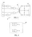
- FIG. 4 illustrates a preferred embodiment for the improved secondary control circuit 42 .
- the secondary control circuit 42 is implemented using two logic OR gates, such that each OR gate receives the control signals used to drive diagonal switching devices and outputs a drive signal to one of the two synchronous rectifiers.
- a first OR gate 52 receives as input the control signals used to drive the first switching device Q A and the fourth switching device Q D ; whereas a second OR gate 54 receives as input the control signals used to drive the third switching device Q B and the third switching device Q C .
- the first OR gate 52 and the second OR gate 54 in turn output drive signals to the first rectifying switch Q 1 and the second rectifying switch Q 2 , respectively.
- the operation of the secondary control circuit 42 is better understood from the timing diagram depicted in FIG. 5 .
- the drive signals for each of the primary switching devices is shown in relation to the drive signals for the synchronous rectifiers as generated by the secondary control circuit 42 .
- substantially complementary drive signals serve as input to the first switching device Q A and the second switching device Q B
- relatively phase shifted substantially complementary control signals serve as input to the third switching device Q C and the fourth switching device Q D .
- diagonal switching devices conduct alternately with a dead time period therebetween.
- a dead time period occurs when the fourth switching device Q D is driven to an off state.
- the second rectifying switch Q 2 is simultaneously driven to an on state.
- the improved secondary control circuit 42 of the present invention provides a delay before the second rectifying switch Q 2 is driven to an on state as shown at 60 .
- the secondary control circuit is operable to drive the second of the two synchronous rectifiers to an on state only after one of the diagonal switching devices is driven to an off state by the primary control circuit.
- the third switching device Q C is driven to an on state.
- This delay between the fourth switching device Q D and the third switching device Q C is set in primary control circuit.
- the second rectifying switch Q 2 is also driven to an on state.
- both of the rectifying switches are turned on during the dead time period and both the inductors on the secondary side are in freewheeling mode.
- the first switching device Q A is driven to an off state.
- the first rectifying switch Q 1 is also driven to an off state.
- the second switching device Q B is driven to an on state.
- diagonal switching device Q B and Q C are in an on state and current flows down through the primary winding of the transformer.
- the improved secondary control circuit of the present invention eliminates the risk of cross conduction between the synchronous rectifiers.
- the improved secondary control circuit may be constructed using a minimal part count as well as takes advantage of the standard delays set in the primary control circuit.
- the improved secondary control circuit allows output choke current to flow in the secondary side of the converter during a portion of the delay period, thereby assisting the soft switching control.
Abstract
An improved secondary control circuit is provided for controlling synchronous rectifiers in a switching power converter. The secondary control circuit employs control signals from a primary control circuit to drive two synchronous rectifiers. In particular, the secondary control circuit is operable to drive both synchronous rectifiers to an on state during a dead time period of operation. The onset of the dead time period occurs when the diagonal conducting switching device is driven to an off state. The secondary control circuit is further operable to drive the second of the two synchronous rectifiers to an on state only after one of the diagonal switching devices has been driven to an off state by the primary control circuit. In this way, the improved secondary control circuit eliminates the risk of cross conduction between the synchronous rectifiers.
Description
The present invention relates generally to switching power supplies and, more particularly, to a simplified control circuit for synchronous rectifiers used in ZVS phase shifted full bridge converters.
Recent advancements in MOSFET switch technology makes synchronous rectifiers a feasible and competitive rectification technique for low voltage, high current DC/DC converters. Synchronous MOSFET switches are used to increase efficiency, reduce power losses, reduce electromagnetic interference and facilitate zero voltage switching (ZVS) in such converters. However, proper timing of the synchronous rectifiers is critical to the efficient operation of the converter.
In one known technique, the synchronous rectifiers may be driven by the control circuit used to drive the primary side of the transformer in the converter. This technique is commonly referred to as control driven synchronous rectification. One proposed implementation of this technique is presented by Laszlo Balogh in “Design Review: 100W, 400 kHz, DC/DC Converter with Current Doubler Synchronous Rectification Achieves 92% Efficiency”, SEM-1100 edition of the Unitrode Switching Regulated Power Supply Design Seminar Manual, by Unitrode corporation, 1996.
In this proposed prior art technique, the DC/DC converter is implemented using a phase shifted full bridge configuration on the primary side and a current doubler output with synchronous rectification on the secondary side. Of particular interest, a secondary control circuit 10 as shown in FIG. 1 is used to drive the synchronous rectifiers (not shown). The secondary control circuit 10 receives as input the primary drive signals 12 for each of the switching devices on the primary side of the converter. The drive signals 12 are in turn transmitted via a signal transformer 14 to the secondary side of the converter. The secondary control circuit 10 then outputs a secondary drive signal 16 for each of the synchronous rectifiers.
Referring to FIG. 2, a timing diagram further illustrates the operation of the prior art secondary control circuit 10. In this proposed technique, both of the synchronous rectifiers are turned on during a dead time period of operation as shown at 22, where a dead period is defined as the time at which no current is flowing from the input voltage source through the primary winding of the transformer of the converter. When diagonal switching devices on the primary side of the transformer are conducting, one of the two synchronous rectifiers is generally in an on state. The onset of a dead time period occurs when one of the two diagonal conducting switching devices is driven to an off state. It should be noted that the second of the two synchronous rectifiers is driven to an on state at the same time as the diagonal switching device is driven to an off state. However, due to parasitic delays and other variations inherent in the switching devices, it is conceivable that the second synchronous rectifier may be driven to an on state before the diagonal conducting switching device is driven to an off state. In this scenario, an opportunity for cross conduction between the synchronous rectifiers is introduced into the converter.
Therefore, it is desirable to provide an improved control circuit for controlling the synchronous rectifiers employed in switching power converters. It is envisioned that the improved control circuit is operable to drive both synchronous rectifiers to an on state during a freewheeling period, and yet eliminate the risk of cross conduction between the synchronous rectifiers.
In accordance with the present invention, an improved secondary control circuit is provided for controlling synchronous rectifiers in a switching power converter. The secondary control circuit employs control signals available for driving primary full bridge switches to drive two synchronous rectifiers. In particular, the secondary control circuit is operable to drive both synchronous rectifiers to an on state during a dead time period of operation. The dead time period is defined as the time at which no current is flowing from the input voltage source through a primary winding of a primary transformer of the converter. The onset of the dead time period occurs when the diagonal conducting switching devices is driven to an off state. In other words, the secondary control circuit is further operable to drive the second of the two synchronous rectifiers to an on state only after one of the diagonal switching devices is driven to an off state by the primary control circuit. In this way, the improved secondary control circuit eliminates the risk of cross conduction between the synchronous rectifiers.
For a more complete understanding of the invention, its objects and advantages, reference may be had to the following specification and to the accompanying drawings.
FIG. 1 is a logical circuit diagram for a conventional secondary control circuit for controlling synchronous rectifiers in a phase shifted full bridge converter circuit;
FIG. 2 is a timing diagram for the conventional secondary control circuit;
FIG. 3 is a schematic of a full bridge converter having current doubler synchronous rectifiers in accordance with the present invention;
FIG. 4 is a logical circuit diagram for an improved secondary control circuit for controlling synchronous rectifiers in accordance with the present invention;
FIG. 5 is a timing diagram for the improved secondary control circuit in accordance with the present invention;
FIG. 6 is a schematic of a full bridge converter having an alternative synchronous rectifier configuration in accordance with the present invention.
A well known full bridge converter 30 having current doubler synchronous rectifiers is depicted in FIG. 3. The converter 30 generally includes an input voltage source 32, a primary switching circuit 34, a transformer 36, a rectifying circuit 38, a primary control circuit 40 and a secondary control circuit 42. While the following description is provided with reference to a full bridge converter, it is readily understood that the broader aspects of the present invention are applicable to other types of converter topologies, such as push pull or half bridge topologies, which may employ synchronous rectification.
The switching circuit 34 includes a first switching device QA and a second switching device QB connected in series to form a first switching leg, and a third switching device QC and a fourth switching device QD connected in series to form a second switching leg. Each of the switching legs is connected in parallel to the input voltage source 32. In a preferred embodiment, the primary switching device are further defined as MOSFET switches.
The switching circuit 34 is in turn connected to a primary winding of the transformer 36. In particular, a first junction point between the first switching device QA and the second switching device QB is connected to one end of the primary winding, and a second junction point between the third switching device QC and the fourth switching device QD is connected to the other end of the primary winding. An inductor Lr is commonly inserted in series with the primary winding of the transformer as shown. The input voltage source 32, the switching circuit 34, and the primary winding of the transformer are collectively referred to as the primary side of the converter.
A primary control circuit 40 operable to generate drive signals for each of the switching devices is connected to the switching circuit 34. In a preferred embodiment, the primary control circuit 34 is operable to supply substantially complementary drive signals to the switching devices in one of the switching legs and relatively phase shifted substantially complementary control signals to the switching devices in the other switching legs, so that diagonal switching devices conduct alternately with a dead time period therebetween. As is well known, the dead time period is defined as the time at which no current is flowing from the input voltage source through a primary winding of a transformer. In other words, the primary control circuit 34 provides zero voltage switching (ZVS) phase shifted control over the switching circuit 34. Although soft switching control is presently preferred, this is not intended as a limitation on the broader aspects of the present invention. On the contrary, hard switching control may be suitably employed by the primary control circuit 34. In this case, external delays may need to be introduced to ensure proper timing of the drive signals as is well known in the art.
The rectifying circuit 38 provides an output voltage VO for the converter. The rectifying circuit 38 generally includes two synchronous rectifiers which are connected to a secondary winding of the transformer 36. Although the present invention is not limited thereto, MOSFET switches are preferably used to implement the synchronous rectifiers.
More specifically, the rectifying circuit 30 includes a first rectifying switch Q1 connected in series with a second rectifying switch Q2. In this configuration, the drain for the first rectifying switch Q1 is connected to one end of the secondary winding of the transformer, the drain for the second rectifying switch Q2 is connected to the other end of the secondary winding of the transformer, and a junction point between the first rectifying switch Q1 and the second rectifying switch Q2 is connected to ground. The rectifying circuit 30 further includes a first inductor L1 connected between the drain of the first rectifying switch Q1 and an output terminal for the output voltage V0 of the converter, and a second inductor L2 connected between the drain of the second rectifying switch Q2 and the output terminal for the output voltage VO. The output voltage V0 is measured across a capacitor C connected between the output terminal and ground. In other words, the rectifying circuit 38 is preferably implemented in a current doubler synchronous rectifier configuration. While the following description is provided with reference to a current doubler synchronous rectifier configuration, it is readily understood that the broader aspects of the present invention are applicable to other types of synchronous rectification circuits. For example, a full bridge converter having an alternative synchronous rectifying circuit is shown in FIG. 6.
In accordance with the present invention, an improved secondary control circuit 42 is connected to the rectifying circuit 38. The secondary control circuit 42 employs control signals from primary control circuit 40 to drive the two synchronous rectifiers. The secondary control circuit is operable to drive both synchronous rectifiers to an on state during a dead time period of operation. When diagonal switching devices on the primary side of the transformer are conducting, one of the two synchronous rectifiers is generally in an on state. The onset of the dead time period occurs when one of the diagonal conducting switching devices is driven to an off state. The secondary control circuit 42 is operable to drive the second of the two synchronous rectifiers to an on state only after one of the diagonal switching devices is driven to an off state by the primary control circuit 34. In particular, the secondary control circuit 42 drives the second of the two synchronous rectifiers to an on state after either delay period, Delay A-B or Delay C-D, as shown in FIG. 5. In this way, the improved secondary control circuit 42 eliminates the risk of cross conduction between the synchronous rectifiers.
FIG. 4 illustrates a preferred embodiment for the improved secondary control circuit 42. The secondary control circuit 42 is implemented using two logic OR gates, such that each OR gate receives the control signals used to drive diagonal switching devices and outputs a drive signal to one of the two synchronous rectifiers. In the context of the above-described full bridge converter, a first OR gate 52 receives as input the control signals used to drive the first switching device QA and the fourth switching device QD; whereas a second OR gate 54 receives as input the control signals used to drive the third switching device QB and the third switching device QC. The first OR gate 52 and the second OR gate 54 in turn output drive signals to the first rectifying switch Q1 and the second rectifying switch Q2, respectively. As will be apparent to one skilled in the art, various hardware configurations may be used to implement the secondary control circuit 42. It is also envisioned that a totem pole or similar buffer stage may be inserted between the output of the secondary control circuit 42 and the synchronous rectifiers to facilitate faster switching.
The operation of the secondary control circuit 42 is better understood from the timing diagram depicted in FIG. 5. The drive signals for each of the primary switching devices is shown in relation to the drive signals for the synchronous rectifiers as generated by the secondary control circuit 42. As noted above, substantially complementary drive signals serve as input to the first switching device QA and the second switching device QB, and relatively phase shifted substantially complementary control signals serve as input to the third switching device QC and the fourth switching device QD. As a result, diagonal switching devices conduct alternately with a dead time period therebetween.
For instance, when diagonal switching devices QA and QD are driven to an on state, current flows up through the primary winding of the transformer. On the secondary side, the first rectifying switch Q1 is in an on state and the second rectifying switch Q2 is in an off state, such that the first inductor L1 freewheels and the second inductor L2 stores energy.
A dead time period occurs when the fourth switching device QD is driven to an off state. As a result, no current is flowing from the input primary source through the primary winding of a transformer. In a conventional approach, the second rectifying switch Q2 is simultaneously driven to an on state. However, the improved secondary control circuit 42 of the present invention provides a delay before the second rectifying switch Q2 is driven to an on state as shown at 60. In other words, the secondary control circuit is operable to drive the second of the two synchronous rectifiers to an on state only after one of the diagonal switching devices is driven to an off state by the primary control circuit.
Next, the third switching device QC is driven to an on state. This delay between the fourth switching device QD and the third switching device QC is set in primary control circuit. When the third switching device QC is driven to an on state, the second rectifying switch Q2 is also driven to an on state. As a result, both of the rectifying switches are turned on during the dead time period and both the inductors on the secondary side are in freewheeling mode. To terminate the freewheeling period, the first switching device QA is driven to an off state. At the same time, the first rectifying switch Q1 is also driven to an off state.
To complete the cycle, the second switching device QB is driven to an on state. As a result, diagonal switching device QB and QC are in an on state and current flows down through the primary winding of the transformer.
Thus, the dead time period is terminated. The cycle is then repeated.
It should be appreciated that the improved secondary control circuit of the present invention eliminates the risk of cross conduction between the synchronous rectifiers. In addition, the improved secondary control circuit may be constructed using a minimal part count as well as takes advantage of the standard delays set in the primary control circuit. Lastly, the improved secondary control circuit allows output choke current to flow in the secondary side of the converter during a portion of the delay period, thereby assisting the soft switching control.
While the invention has been described in its presently preferred form, it will be understood that the invention is capable of modification without departing from the spirit of the invention as set forth in the appended claims.
Claims (26)
1. A method for controlling two synchronous rectifiers in a switching power converter, comprising:
providing two diagonal switching device in a conducting state and; one of the two synchronous rectifiers in an on state;
driving one of two diagonal conducting switching devices to an off state, thereby initiating a dead time period of operation during which no current flows through a primary winding of a transformer; and
driving the other of the two synchronous rectifiers to an on state after said one of two diagonal conducting switching devices has been driven to an off state, thereby driving each of the two synchronous rectifiers to an on state during the dead time period.
2. The method of claim 1 further comprises the step of using drive signals for the diagonal switching devices to drive the two synchronous rectifiers.
3. The method of claim 2 further comprises the step of using two logic OR gates to drive the two synchronous rectifiers.
4. The method of claim 1 wherein the switching power converter is further defined as a substantially zero voltage switching phase shifted full bridge converter having a current doubler synchronous rectifier.
5. A switching power converter, comprising:
an input voltage source;
a transformer having a primary winding and a secondary winding;
a switching circuit connected to the primary winding of the transformer for providing bidirectional current flow there through, the switching circuit having a first pair and a second pair of diagonal switching devices;
a rectifying circuit, having two synchronous rectifiers, connected to the secondary winding of the transformer for providing an output voltage of the converter;
a primary control circuit connected to the switching circuit and operable to generate drive signals for the switching device, such that each pair of diagonal switching devices conduct alternately with a dead time period therebetween and the dead time period is initiated when one of the conducting diagonal switching devices is driven to an off state; and
a secondary control circuit connected to the rectifying circuit and operable to drive the two synchronous rectifiers to an on state during the dead time period, such that one of the conducting diagonal switching devices is driven to an off state prior to the second of the two synchronous rectifiers being driven to an on state.
6. The switching power converter of claim 5 wherein the dead time period is indicative of no current flowing through the primary winding of the transformer.
7. The switching power converter of claim 5 wherein the secondary control circuit employs the control signals from the primary control circuit to drive the two synchronous rectifiers of the rectifying circuit.
8. The switching power converter of claim 7 wherein the secondary control circuit further includes two logic OR gates, such that each OR gate receives the controls signals used to drive diagonal switching devices and outputs a control signal to one of the two synchronous rectifiers.
9. The switching power converter of claim 5 wherein the switching devices are further defined as MOSFET switches.
10. The switching power converter of claim 5 wherein the two synchronous rectifiers are further defined as MOSFET switches.
11. The switching power converter of claim 5 is further defined as a substantially zero voltage switching phase shifted full bridge converter.
12. A switching power converter, comprising:
an input voltage source;
a switching circuit having a first switching device and a second switching device connected in series to form a first switching leg, and a third switching device and a fourth switching device connected in series to form a second switching leg, each of the switching legs connected in parallel with the input voltage source;
a transformer having a primary winding and a secondary winding, one end of the primary winding being connected to a junction point between the first switching device and the second switching device and the other end of the primary winding being connected to a junction point between the third switching device and the fourth switching device;
a rectifying circuit, having two synchronous rectifiers, connected to the secondary winding of the transformer for providing an output voltage of the converter;
a primary control circuit connected to the switching circuit, the primary control circuit operable to supply substantially complementary control signals to the switching devices in one of the switching legs and relatively phase shifted substantially complementary control signals to the switching devices in the other switching legs, so that diagonal switching devices conduct alternately with a dead time period therebetween and the dead time period is initiated when one of the conducting diagonal switching devices is driven to an off state; and
a secondary control circuit connected to the rectifying circuit, the secondary control circuit operable to drive the two synchronous rectifiers to an on state during the dead time period, such that said one of the conducting diagonal switching devices is driven to an off state by the primary control circuit prior to the second of the two synchronous rectifiers being driven to an on state.
13. The switching power converter of claim 12 wherein the dead time period is indicative of no current flowing through the primary winding of the transformer.
14. The switching power converter of claim 12 wherein the secondary control circuit employs the control signals from the primary control circuit to drive the two synchronous rectifiers of the rectifying circuit.
15. The switching power converter of claim 12 wherein the secondary control circuit further includes two logic OR gates, such that each OR gate receives the controls signals used to drive diagonal switching devices and outputs a control signal to one of the two synchronous rectifiers.
16. The switching power converter of claim 12 wherein the switching devices are further defined as MOSFET switches.
17. The switching power converter of claim 12 is further defined as a substantially zero voltage switching phase shifted full bridge converter.
18. The switching power converter of claim 12 wherein the two synchronous rectifiers are further defined as MOSFET switches.
19. The switching power converter of claim 12 wherein the rectifying circuit includes a first MOSFET switch connected in series with a second MOSFET switch, a drain of the first MOSFET switch being connected to one end of the secondary winding of the transformer, a drain of the second MOSFET switch being connected to the other end of the secondary winding of the transformer, and a junction point between the first MOSFET switch and the second MOSFET switch connected to ground.
20. The switching power converter of claim 19 wherein the rectifying circuit further includes a first inductor connected between the drain of the first MOSFET switch and an output terminal for the output voltage of the converter and a second inductor connected between the source of the second MOSFET switch and the output terminal for the output voltage of the converter.
21. A switching power converter, comprising:
an input voltage source;
a switching circuit having a first switching device and a second switching device connected in series to form a first switching leg, and a third switching device and a fourth switching device connected in series to form a second switching leg, each of the switching legs connected in parallel with the input voltage source;
a transformer having a primary winding and a secondary winding, one end of the primary winding being connected to a junction point between the first switching device and the second. switching device and the other end of the primary winding being connected to a junction point between the third switching device and the fourth switching device;
a rectifying circuit, having two synchronous rectifiers, connected to the secondary winding of the transformer for providing an output voltage of the converter;
a primary control circuit connected to the switching circuit and operable to generate a drive signal for each of the switching devices; and
a secondary control circuit having a first logic OR gate and a second logic OR gate, the first OR gate receives the drive signals used to control the first and fourth switching devices and outputs a drive signal to one of the two synchronous rectifiers, and the second OR gate receives the drive signals used to control the second and third switching devices and outputs a drive signal to the other of the two synchronous rectifiers.
22. The switching power converter of claim 21 wherein the primary control circuit is operable to supply substantially complementary control signals to the switching devices in one of the switching legs and relatively phase shifted substantially complementary control signals to the switching devices in the other switching legs, so that diagonal switching devices conduct alternately with a dead time period therebetween and the dead time period is initiated when one of the conducting diagonal switching devices is driven to an off state.
23. The switching power converter of claim 22 wherein the secondary control circuit is operable to drive the two synchronous rectifiers to an on state during the dead time period, such that said one of the conducting diagonal switching devices is driven to an off state by the primary control circuit prior to the second of the two synchronous rectifiers being driven to an on state.
24. The switching power converter of claim 21 wherein the switching devices are further defined as MOSFET switches.
25. The switching power converter of claim 21 is further defined as a substantially zero voltage switching phase shifted full bridge converter.
26. The switching power converter of claim 21 wherein the rectifying circuit is defined as a current doubler synchronous rectifier.
Priority Applications (1)
| Application Number | Priority Date | Filing Date | Title |
|---|---|---|---|
| US09/861,367 US6504739B2 (en) | 2001-05-18 | 2001-05-18 | Simple control circuit for synchronous rectifiers used in ZVS phase shifted full bridge converter |
Applications Claiming Priority (1)
| Application Number | Priority Date | Filing Date | Title |
|---|---|---|---|
| US09/861,367 US6504739B2 (en) | 2001-05-18 | 2001-05-18 | Simple control circuit for synchronous rectifiers used in ZVS phase shifted full bridge converter |
Publications (2)
| Publication Number | Publication Date |
|---|---|
| US20020172061A1 US20020172061A1 (en) | 2002-11-21 |
| US6504739B2 true US6504739B2 (en) | 2003-01-07 |
Family
ID=25335602
Family Applications (1)
| Application Number | Title | Priority Date | Filing Date |
|---|---|---|---|
| US09/861,367 Expired - Fee Related US6504739B2 (en) | 2001-05-18 | 2001-05-18 | Simple control circuit for synchronous rectifiers used in ZVS phase shifted full bridge converter |
Country Status (1)
| Country | Link |
|---|---|
| US (1) | US6504739B2 (en) |
Cited By (34)
| Publication number | Priority date | Publication date | Assignee | Title |
|---|---|---|---|---|
| US20040047164A1 (en) * | 2001-02-01 | 2004-03-11 | Brkovic Milivoje S. | Isolated drive circuitry used in switch-mode power converters |
| US20040052100A1 (en) * | 2002-07-04 | 2004-03-18 | Chia-Hsiong Huang | Synchronous rectifier |
| US20040136209A1 (en) * | 2003-01-09 | 2004-07-15 | Renesas Technology Corp. | Switching power supply device and the semiconductor integrated circuit for power supply control |
| US20040246748A1 (en) * | 2003-06-05 | 2004-12-09 | Ming Xu | Bridge-buck converter with self-driven synchronous rectifiers |
| US20060120123A1 (en) * | 2004-12-02 | 2006-06-08 | Astec International Limited | Method and apparatus for reducing body diode conduction of synchronous rectifiers |
| US7102898B2 (en) | 2001-02-01 | 2006-09-05 | Di/Dt, Inc. | Isolated drive circuitry used in switch-mode power converters |
| US7200012B1 (en) * | 2006-02-21 | 2007-04-03 | Niko Semiconductor Co., Ltd. | Circuit utilizing a push-pull pulse width modulator to control a full-bridge inverter |
| US20070076458A1 (en) * | 2005-09-30 | 2007-04-05 | Honeywell International, Inc. | Timing control circuit for lossless switching converter |
| US20070103819A1 (en) * | 2004-04-30 | 2007-05-10 | Williams David A | Self Driven Synchronous Rectifier Shutdown Circuit and Method |
| CN100403646C (en) * | 2004-02-23 | 2008-07-16 | 联昌电子企业股份有限公司 | Circuit for driving full bridge type current converter by using push pull type control chip |
| CN100423437C (en) * | 2004-08-05 | 2008-10-01 | 尼克森微电子股份有限公司 | Bridge synchronization rectification circuit with dead time adjustment |
| US20090135631A1 (en) * | 2007-11-23 | 2009-05-28 | Ta-Yung Yang | Method and apparatus of providing synchronous rectifying and regulation for power converters |
| US7548436B1 (en) * | 2008-06-17 | 2009-06-16 | Lite-On Technology | Driving circuit and a power converter incorporating the same |
| US20100226154A1 (en) * | 2009-03-03 | 2010-09-09 | National Taiwan University Of Science & Technology | Power converters |
| CN102111074A (en) * | 2011-03-30 | 2011-06-29 | 华南理工大学 | Method and device for reducing switching loss of phase-shifting full-bridge converter |
| US20120120683A1 (en) * | 2010-11-17 | 2012-05-17 | Acbel Polytech Inc. | Full bridge phase shifted power supply with synchronous rectification and current doubler and method for dynamically adjusting delay parameters thereof |
| KR101228799B1 (en) | 2010-12-24 | 2013-01-31 | 한국과학기술원 | Power supply |
| KR101240746B1 (en) * | 2010-12-16 | 2013-03-11 | 한국과학기술원 | Power converter integrating flyback converter |
| DE102011086219A1 (en) | 2011-11-11 | 2013-05-16 | Panasonic Corporation | Switching power supply apparatus e.g. quasi-resonant clocked power converter, has control circuit to control switches and switch circuit, so that current in transformer is with same polarity as transformed current of inverter circuit |
| US20130188400A1 (en) * | 2012-01-20 | 2013-07-25 | The Ohio State University | Enhanced flyback converter |
| DE102012201642A1 (en) | 2012-02-03 | 2013-08-08 | Panasonic Corporation | Resonance converter i.e. power switch, for switched mode power supply, has voltage output unit for outputting voltage received by smoothing circuit, and signal processor for controlling on/off switching processes of switching circuit |
| KR101305615B1 (en) | 2011-09-15 | 2013-09-09 | 엘지이노텍 주식회사 | Switching power supply circuit |
| KR101333980B1 (en) | 2011-05-25 | 2013-11-27 | 히다찌 미토 엔지니어링 가부시끼가이샤 | Dc power supply |
| KR101408600B1 (en) | 2013-01-25 | 2014-06-17 | 삼성전기주식회사 | Switching converter and ac adapter using the same |
| US20140177282A1 (en) * | 2012-12-21 | 2014-06-26 | Korea Advanced Institute Of Science And Technology | Power supply device |
| US8797773B2 (en) | 2010-08-30 | 2014-08-05 | Cooper Technologies Company | Isolated DC-DC converter including ZVS full-bridge and current doubler |
| KR101428392B1 (en) | 2013-05-31 | 2014-08-08 | 현대자동차주식회사 | Full bridge DC-DC converter with current doubler |
| KR101434497B1 (en) | 2012-11-19 | 2014-08-27 | 주식회사 동아일렉콤 | An apparatus and a method for power conversion |
| KR101442553B1 (en) * | 2013-05-09 | 2014-09-26 | 홍성수 | Power circuit |
| KR101464478B1 (en) * | 2013-07-15 | 2014-11-24 | 주식회사 동아일렉콤 | Multi input llc resonant type dc-dc converter |
| KR101515866B1 (en) | 2013-10-16 | 2015-05-06 | (주)갑진 | D.C. distribution system having low frequency transformer |
| KR101519490B1 (en) * | 2013-12-13 | 2015-05-13 | 경북대학교 산학협력단 | full bridge converter comprising switching cells and electronic device using the full bridge converter |
| WO2015127824A1 (en) * | 2014-02-26 | 2015-09-03 | 联合汽车电子有限公司 | Double-loop control circuit of phase-shift full-bridge synchronous rectification circuit |
| US20170317599A1 (en) * | 2014-12-05 | 2017-11-02 | Panasonic Intellectual Property Management Co., Ltd. | Switching power supply device |
Families Citing this family (17)
| Publication number | Priority date | Publication date | Assignee | Title |
|---|---|---|---|---|
| US7800921B2 (en) * | 2007-01-08 | 2010-09-21 | Continental Automotive Systems Us, Inc. | DC/DC converter |
| US8159837B2 (en) * | 2008-10-27 | 2012-04-17 | International Business Machines Corporation | Integrated bias and standby power supply circuit |
| WO2010069096A1 (en) * | 2008-12-19 | 2010-06-24 | Texas Instruments Incorporated | Fixed-frequency llc resonant power regulator |
| US8717782B2 (en) * | 2009-01-07 | 2014-05-06 | Texas Instruments Incorporated | Sweeping frequency LLC resonant power regulator |
| US8787044B2 (en) * | 2009-05-07 | 2014-07-22 | Flextronics Ap, Llc | Energy recovery snubber circuit for power converters |
| ITFO20100011A1 (en) * | 2010-10-25 | 2012-04-26 | Polar Srl | CONTROLLED ELECTRICAL CURRENT GENERATOR DEVICE AND RELATIVE ELECTRICAL CURRENT GENERATION PROCEDURE |
| WO2013020269A1 (en) * | 2011-08-09 | 2013-02-14 | 联合汽车电子有限公司 | Phase-shift full-bridge circuit and control method thereof |
| US9270189B2 (en) * | 2012-05-18 | 2016-02-23 | General Electric Company | Power converter and method |
| US9859803B2 (en) * | 2013-04-23 | 2018-01-02 | Analog Devices Global | Transformer-based isolated bi-directional DC-DC power converter, and method and controller for using same |
| US9837920B2 (en) | 2013-09-27 | 2017-12-05 | Bel Power Solutions, Inc. | Commutation current steering method in a zero volt switching power converter using a synchronous rectifier |
| JP6504832B2 (en) | 2014-01-28 | 2019-04-24 | ゼネラル・エレクトリック・カンパニイ | Integrated mounting and cooling devices, electronic devices and vehicles |
| KR102357022B1 (en) * | 2014-09-12 | 2022-01-28 | 현대모비스 주식회사 | Method and device for controlling synchoronizing rectification ldc |
| US10073512B2 (en) | 2014-11-19 | 2018-09-11 | General Electric Company | System and method for full range control of dual active bridge |
| WO2016125374A1 (en) * | 2015-02-02 | 2016-08-11 | 三菱電機株式会社 | Dc/dc converter |
| JP6817563B2 (en) * | 2015-12-14 | 2021-01-20 | パナソニックIpマネジメント株式会社 | Power transmission system and controller |
| CN105656298B (en) * | 2016-04-11 | 2018-01-05 | 北京国铁路阳技术有限公司 | A kind of peak point current current-limiting apparatus based on DSP+CPLD controls |
| US10396671B2 (en) * | 2017-01-20 | 2019-08-27 | Astec International Limited | Power supplies having power switches controllable with a varying frequency, duty cycle and/or phase to regulate outputs |
Citations (44)
| Publication number | Priority date | Publication date | Assignee | Title |
|---|---|---|---|---|
| US4864479A (en) | 1988-03-07 | 1989-09-05 | General Electric Company | Full-bridge lossless switching converter |
| US4884186A (en) | 1987-12-10 | 1989-11-28 | Boschert Incorporated | Power supply with reduced switching losses |
| US4912622A (en) | 1988-03-07 | 1990-03-27 | General Electric Company | Gate driver for a full-bridge lossless switching device |
| US4953068A (en) | 1989-11-08 | 1990-08-28 | Unisys Corporation | Full bridge power converter with multiple zero voltage resonant transition switching |
| US4967332A (en) | 1990-02-26 | 1990-10-30 | General Electric Company | HVIC primary side power supply controller including full-bridge/half-bridge driver |
| US5027264A (en) | 1989-09-29 | 1991-06-25 | Wisconsin Alumni Research Foundation | Power conversion apparatus for DC/DC conversion using dual active bridges |
| US5099202A (en) | 1990-02-26 | 1992-03-24 | General Electric Company | Phase shift generator |
| USRE33866E (en) * | 1989-07-13 | 1992-03-31 | General Electric Company | Resonant inverter employing frequency and phase modulation using optimal trajectory control |
| US5132888A (en) | 1991-01-07 | 1992-07-21 | Unisys Corporation | Interleaved bridge converter |
| US5132889A (en) | 1991-05-15 | 1992-07-21 | Ibm Corporation | Resonant-transition DC-to-DC converter |
| US5140509A (en) * | 1991-11-08 | 1992-08-18 | Allied-Signal Inc. | Regulated bi-directional DC-to-DC voltage converter |
| US5157593A (en) | 1990-12-13 | 1992-10-20 | Northern Telecom Limited | Constant frequency resonant dc/dc converter |
| US5157592A (en) | 1991-10-15 | 1992-10-20 | International Business Machines Corporation | DC-DC converter with adaptive zero-voltage switching |
| US5189969A (en) | 1991-02-12 | 1993-03-02 | Brother Kogyo Kabushiki Kaisha | Device for processing sheet material with colored pattern |
| US5208738A (en) | 1990-12-13 | 1993-05-04 | Northern Telecom Limited | Constant frequency resonant DC/DC converter |
| US5227961A (en) | 1990-02-26 | 1993-07-13 | General Electric Company | Symmetrical delay circuit |
| US5231563A (en) * | 1990-09-07 | 1993-07-27 | Itt Corporation | Square wave converter having an improved zero voltage switching operation |
| US5245520A (en) * | 1991-10-10 | 1993-09-14 | Paul Imbertson | Asymmetrical duty cycle power converter |
| US5255174A (en) * | 1991-10-18 | 1993-10-19 | Allied-Signal Inc. | Regulated bi-directional DC-to-DC voltage converter which maintains a continuous input current during step-up conversion |
| US5291384A (en) | 1991-06-20 | 1994-03-01 | Unitrode Corporation | Phase shifted switching controller |
| US5315498A (en) | 1992-12-23 | 1994-05-24 | International Business Machines Corporation | Apparatus providing leading leg current sensing for control of full bridge power supply |
| US5438497A (en) | 1993-05-13 | 1995-08-01 | Northern Telecom Limited | Tertiary side resonant DC/DC converter |
| US5442540A (en) | 1992-06-12 | 1995-08-15 | The Center For Innovative Technology | Soft-switching PWM converters |
| US5481449A (en) | 1994-03-21 | 1996-01-02 | General Electric Company | Efficient, high power density, high power factor converter for very low dc voltage applications |
| US5539630A (en) | 1993-11-15 | 1996-07-23 | California Institute Of Technology | Soft-switching converter DC-to-DC isolated with voltage bidirectional switches on the secondary side of an isolation transformer |
| US5546294A (en) | 1995-07-24 | 1996-08-13 | General Electric Company | Resonant converter with wide load range |
| US5563775A (en) | 1994-06-16 | 1996-10-08 | Reliance Comm/Tech Corporation | Full bridge phase displaced resonant transition circuit for obtaining constant resonant transition current from 0° phase angle to 180° phase angle |
| US5610508A (en) | 1994-06-16 | 1997-03-11 | Reltec Corporation | Circuitry to maintain proper current transformer operation |
| US5619401A (en) | 1994-06-02 | 1997-04-08 | Telefonaktiebolaget Lm Ericsson | Circuit arrangement |
| US5675476A (en) | 1995-06-01 | 1997-10-07 | Nostwick; Allan A. | Phase controlled bridge |
| US5684683A (en) | 1996-02-09 | 1997-11-04 | Wisconsin Alumni Research Foundation | DC-to-DC power conversion with high current output |
| US5781419A (en) | 1996-04-12 | 1998-07-14 | Soft Switching Technologies, Inc. | Soft switching DC-to-DC converter with coupled inductors |
| US5864471A (en) | 1997-03-28 | 1999-01-26 | Kammiller; Neil A. | Energy recovery circuit for use in a converter |
| US5875103A (en) | 1995-12-22 | 1999-02-23 | Electronic Measurements, Inc. | Full range soft-switching DC-DC converter |
| US5877947A (en) | 1997-07-30 | 1999-03-02 | Lucent Technologies Inc. | Snubber circuit for a rectifier and method of operation thereof |
| US5898581A (en) | 1997-08-27 | 1999-04-27 | Lucent Technologies Inc. | Active snubber for buck-based converters and method of operation thereof |
| US5910886A (en) | 1997-11-07 | 1999-06-08 | Sierra Applied Sciences, Inc. | Phase-shift power supply |
| US5923547A (en) | 1998-01-22 | 1999-07-13 | Lucent Technologies | Snubber circuit for a power converter and method of operation thereof |
| US5946200A (en) | 1995-12-02 | 1999-08-31 | Korea Electrotechnology Research Institute | Circulating current free type high frequency soft switching pulsewidth modulated full bridge DC/DC converter |
| US5986912A (en) * | 1998-07-03 | 1999-11-16 | Delta Electronics Inc. | Compact assembly configuration and process for reducing lead wire connections and solder joints |
| US6016258A (en) | 1998-10-02 | 2000-01-18 | Nortel Networks Corporation | Full bridge DC-DC converters |
| US6038148A (en) | 1998-12-11 | 2000-03-14 | Ericsson, Inc. | Self-driven synchronous rectification scheme |
| US6219264B1 (en) * | 1999-07-29 | 2001-04-17 | Intel Corporation | Method and apparatus to reduce rectifier loss |
| US6275401B1 (en) * | 2000-01-10 | 2001-08-14 | Power-One, Inc. | Self-driven synchronous rectification circuit for low output voltage DC-DC converters |
-
2001
- 2001-05-18 US US09/861,367 patent/US6504739B2/en not_active Expired - Fee Related
Patent Citations (44)
| Publication number | Priority date | Publication date | Assignee | Title |
|---|---|---|---|---|
| US4884186A (en) | 1987-12-10 | 1989-11-28 | Boschert Incorporated | Power supply with reduced switching losses |
| US4912622A (en) | 1988-03-07 | 1990-03-27 | General Electric Company | Gate driver for a full-bridge lossless switching device |
| US4864479A (en) | 1988-03-07 | 1989-09-05 | General Electric Company | Full-bridge lossless switching converter |
| USRE33866E (en) * | 1989-07-13 | 1992-03-31 | General Electric Company | Resonant inverter employing frequency and phase modulation using optimal trajectory control |
| US5027264A (en) | 1989-09-29 | 1991-06-25 | Wisconsin Alumni Research Foundation | Power conversion apparatus for DC/DC conversion using dual active bridges |
| US4953068A (en) | 1989-11-08 | 1990-08-28 | Unisys Corporation | Full bridge power converter with multiple zero voltage resonant transition switching |
| US5227961A (en) | 1990-02-26 | 1993-07-13 | General Electric Company | Symmetrical delay circuit |
| US5099202A (en) | 1990-02-26 | 1992-03-24 | General Electric Company | Phase shift generator |
| US4967332A (en) | 1990-02-26 | 1990-10-30 | General Electric Company | HVIC primary side power supply controller including full-bridge/half-bridge driver |
| US5231563A (en) * | 1990-09-07 | 1993-07-27 | Itt Corporation | Square wave converter having an improved zero voltage switching operation |
| US5157593A (en) | 1990-12-13 | 1992-10-20 | Northern Telecom Limited | Constant frequency resonant dc/dc converter |
| US5208738A (en) | 1990-12-13 | 1993-05-04 | Northern Telecom Limited | Constant frequency resonant DC/DC converter |
| US5132888A (en) | 1991-01-07 | 1992-07-21 | Unisys Corporation | Interleaved bridge converter |
| US5189969A (en) | 1991-02-12 | 1993-03-02 | Brother Kogyo Kabushiki Kaisha | Device for processing sheet material with colored pattern |
| US5132889A (en) | 1991-05-15 | 1992-07-21 | Ibm Corporation | Resonant-transition DC-to-DC converter |
| US5291384A (en) | 1991-06-20 | 1994-03-01 | Unitrode Corporation | Phase shifted switching controller |
| US5245520A (en) * | 1991-10-10 | 1993-09-14 | Paul Imbertson | Asymmetrical duty cycle power converter |
| US5157592A (en) | 1991-10-15 | 1992-10-20 | International Business Machines Corporation | DC-DC converter with adaptive zero-voltage switching |
| US5255174A (en) * | 1991-10-18 | 1993-10-19 | Allied-Signal Inc. | Regulated bi-directional DC-to-DC voltage converter which maintains a continuous input current during step-up conversion |
| US5140509A (en) * | 1991-11-08 | 1992-08-18 | Allied-Signal Inc. | Regulated bi-directional DC-to-DC voltage converter |
| US5442540A (en) | 1992-06-12 | 1995-08-15 | The Center For Innovative Technology | Soft-switching PWM converters |
| US5315498A (en) | 1992-12-23 | 1994-05-24 | International Business Machines Corporation | Apparatus providing leading leg current sensing for control of full bridge power supply |
| US5438497A (en) | 1993-05-13 | 1995-08-01 | Northern Telecom Limited | Tertiary side resonant DC/DC converter |
| US5539630A (en) | 1993-11-15 | 1996-07-23 | California Institute Of Technology | Soft-switching converter DC-to-DC isolated with voltage bidirectional switches on the secondary side of an isolation transformer |
| US5481449A (en) | 1994-03-21 | 1996-01-02 | General Electric Company | Efficient, high power density, high power factor converter for very low dc voltage applications |
| US5619401A (en) | 1994-06-02 | 1997-04-08 | Telefonaktiebolaget Lm Ericsson | Circuit arrangement |
| US5563775A (en) | 1994-06-16 | 1996-10-08 | Reliance Comm/Tech Corporation | Full bridge phase displaced resonant transition circuit for obtaining constant resonant transition current from 0° phase angle to 180° phase angle |
| US5610508A (en) | 1994-06-16 | 1997-03-11 | Reltec Corporation | Circuitry to maintain proper current transformer operation |
| US5675476A (en) | 1995-06-01 | 1997-10-07 | Nostwick; Allan A. | Phase controlled bridge |
| US5546294A (en) | 1995-07-24 | 1996-08-13 | General Electric Company | Resonant converter with wide load range |
| US5946200A (en) | 1995-12-02 | 1999-08-31 | Korea Electrotechnology Research Institute | Circulating current free type high frequency soft switching pulsewidth modulated full bridge DC/DC converter |
| US5875103A (en) | 1995-12-22 | 1999-02-23 | Electronic Measurements, Inc. | Full range soft-switching DC-DC converter |
| US5684683A (en) | 1996-02-09 | 1997-11-04 | Wisconsin Alumni Research Foundation | DC-to-DC power conversion with high current output |
| US5781419A (en) | 1996-04-12 | 1998-07-14 | Soft Switching Technologies, Inc. | Soft switching DC-to-DC converter with coupled inductors |
| US5864471A (en) | 1997-03-28 | 1999-01-26 | Kammiller; Neil A. | Energy recovery circuit for use in a converter |
| US5877947A (en) | 1997-07-30 | 1999-03-02 | Lucent Technologies Inc. | Snubber circuit for a rectifier and method of operation thereof |
| US5898581A (en) | 1997-08-27 | 1999-04-27 | Lucent Technologies Inc. | Active snubber for buck-based converters and method of operation thereof |
| US5910886A (en) | 1997-11-07 | 1999-06-08 | Sierra Applied Sciences, Inc. | Phase-shift power supply |
| US5923547A (en) | 1998-01-22 | 1999-07-13 | Lucent Technologies | Snubber circuit for a power converter and method of operation thereof |
| US5986912A (en) * | 1998-07-03 | 1999-11-16 | Delta Electronics Inc. | Compact assembly configuration and process for reducing lead wire connections and solder joints |
| US6016258A (en) | 1998-10-02 | 2000-01-18 | Nortel Networks Corporation | Full bridge DC-DC converters |
| US6038148A (en) | 1998-12-11 | 2000-03-14 | Ericsson, Inc. | Self-driven synchronous rectification scheme |
| US6219264B1 (en) * | 1999-07-29 | 2001-04-17 | Intel Corporation | Method and apparatus to reduce rectifier loss |
| US6275401B1 (en) * | 2000-01-10 | 2001-08-14 | Power-One, Inc. | Self-driven synchronous rectification circuit for low output voltage DC-DC converters |
Non-Patent Citations (1)
| Title |
|---|
| Laszlo Balogh, "Design Review: 100W, 400kHz, DC/DC Converter with Current Doubler Synchronous Rectificatin Achieves 92% Efficiency", SEM-1100 edition of the Unitrode Switching Regulated Power Supply Design Seminar Manual, by Unitrode corporation, 1996. |
Cited By (55)
| Publication number | Priority date | Publication date | Assignee | Title |
|---|---|---|---|---|
| US6791851B2 (en) | 2001-02-01 | 2004-09-14 | Di/Dt, Inc. | Isolated drive circuitry used in switch-mode power converters |
| US6804125B2 (en) * | 2001-02-01 | 2004-10-12 | Di/Dt Inc. | Isolated drive circuitry used in switch-mode power converters |
| US20040047164A1 (en) * | 2001-02-01 | 2004-03-11 | Brkovic Milivoje S. | Isolated drive circuitry used in switch-mode power converters |
| US7102898B2 (en) | 2001-02-01 | 2006-09-05 | Di/Dt, Inc. | Isolated drive circuitry used in switch-mode power converters |
| US20040052100A1 (en) * | 2002-07-04 | 2004-03-18 | Chia-Hsiong Huang | Synchronous rectifier |
| US6940738B2 (en) * | 2002-07-04 | 2005-09-06 | Delta Electronics, Inc. | Synchronous rectifier |
| US7158392B2 (en) * | 2003-01-09 | 2007-01-02 | Renesas Technology Corp. | Switching power supply device and the semiconductor integrated circuit for power supply control |
| US20040136209A1 (en) * | 2003-01-09 | 2004-07-15 | Renesas Technology Corp. | Switching power supply device and the semiconductor integrated circuit for power supply control |
| US20040246748A1 (en) * | 2003-06-05 | 2004-12-09 | Ming Xu | Bridge-buck converter with self-driven synchronous rectifiers |
| US6859372B2 (en) * | 2003-06-05 | 2005-02-22 | Virginia Tech Intellectual Properties, Inc. | Bridge-buck converter with self-driven synchronous rectifiers |
| CN100403646C (en) * | 2004-02-23 | 2008-07-16 | 联昌电子企业股份有限公司 | Circuit for driving full bridge type current converter by using push pull type control chip |
| US20070103819A1 (en) * | 2004-04-30 | 2007-05-10 | Williams David A | Self Driven Synchronous Rectifier Shutdown Circuit and Method |
| US7333350B2 (en) * | 2004-04-30 | 2008-02-19 | Power One, Inc. | Self driven synchronous rectifier shutdown circuit and method |
| CN100423437C (en) * | 2004-08-05 | 2008-10-01 | 尼克森微电子股份有限公司 | Bridge synchronization rectification circuit with dead time adjustment |
| US20060120123A1 (en) * | 2004-12-02 | 2006-06-08 | Astec International Limited | Method and apparatus for reducing body diode conduction of synchronous rectifiers |
| US7499299B2 (en) | 2004-12-02 | 2009-03-03 | Astec International Limited | Method and apparatus for reducing body diode conduction of synchronous rectifiers |
| US7262980B2 (en) | 2004-12-02 | 2007-08-28 | Astec International Limited | Method and apparatus for reducing body diode conduction of synchronous rectifiers |
| US20080031027A1 (en) * | 2004-12-02 | 2008-02-07 | Astec International Limited | Method and Apparatus for Reducing Body Diode Conduction of Synchronous Rectifiers |
| US7327178B2 (en) * | 2005-09-30 | 2008-02-05 | Honeywell International, Inc. | Timing control circuit for lossless switching converter |
| US20070076458A1 (en) * | 2005-09-30 | 2007-04-05 | Honeywell International, Inc. | Timing control circuit for lossless switching converter |
| US7200012B1 (en) * | 2006-02-21 | 2007-04-03 | Niko Semiconductor Co., Ltd. | Circuit utilizing a push-pull pulse width modulator to control a full-bridge inverter |
| US20090135631A1 (en) * | 2007-11-23 | 2009-05-28 | Ta-Yung Yang | Method and apparatus of providing synchronous rectifying and regulation for power converters |
| US7903440B2 (en) * | 2007-11-23 | 2011-03-08 | System General Corp. | Synchronous regulation circuit and method for providing synchronous regulation for power converters |
| US7548436B1 (en) * | 2008-06-17 | 2009-06-16 | Lite-On Technology | Driving circuit and a power converter incorporating the same |
| US20100226154A1 (en) * | 2009-03-03 | 2010-09-09 | National Taiwan University Of Science & Technology | Power converters |
| US7957161B2 (en) | 2009-03-03 | 2011-06-07 | National Taiwan University Of Science And Technology | Power converters |
| US8797773B2 (en) | 2010-08-30 | 2014-08-05 | Cooper Technologies Company | Isolated DC-DC converter including ZVS full-bridge and current doubler |
| US20120120683A1 (en) * | 2010-11-17 | 2012-05-17 | Acbel Polytech Inc. | Full bridge phase shifted power supply with synchronous rectification and current doubler and method for dynamically adjusting delay parameters thereof |
| US8824168B2 (en) * | 2010-11-17 | 2014-09-02 | Acbel Polytech Inc. | Dynamically adjusting drive signals for full bridge phase shifted converter and current doubler synchronous rectifier |
| KR101240746B1 (en) * | 2010-12-16 | 2013-03-11 | 한국과학기술원 | Power converter integrating flyback converter |
| US8787041B2 (en) | 2010-12-16 | 2014-07-22 | Samsung Electro-Mechanics Co., Ltd. | Power converter integrated with flyback converter |
| KR101228799B1 (en) | 2010-12-24 | 2013-01-31 | 한국과학기술원 | Power supply |
| CN102111074A (en) * | 2011-03-30 | 2011-06-29 | 华南理工大学 | Method and device for reducing switching loss of phase-shifting full-bridge converter |
| KR101333980B1 (en) | 2011-05-25 | 2013-11-27 | 히다찌 미토 엔지니어링 가부시끼가이샤 | Dc power supply |
| KR101305615B1 (en) | 2011-09-15 | 2013-09-09 | 엘지이노텍 주식회사 | Switching power supply circuit |
| US9369034B2 (en) | 2011-09-15 | 2016-06-14 | Lg Innotek Co., Ltd. | Switching power supply circuit using switching devices and switching controller |
| DE102011086219A1 (en) | 2011-11-11 | 2013-05-16 | Panasonic Corporation | Switching power supply apparatus e.g. quasi-resonant clocked power converter, has control circuit to control switches and switch circuit, so that current in transformer is with same polarity as transformed current of inverter circuit |
| US20180123480A1 (en) * | 2012-01-20 | 2018-05-03 | Ohio State Innovation Foundation | Enhanced flyback converter |
| US9413257B2 (en) * | 2012-01-20 | 2016-08-09 | The Ohio State University | Enhanced flyback converter |
| US20130188400A1 (en) * | 2012-01-20 | 2013-07-25 | The Ohio State University | Enhanced flyback converter |
| DE102012201642A1 (en) | 2012-02-03 | 2013-08-08 | Panasonic Corporation | Resonance converter i.e. power switch, for switched mode power supply, has voltage output unit for outputting voltage received by smoothing circuit, and signal processor for controlling on/off switching processes of switching circuit |
| KR101434497B1 (en) | 2012-11-19 | 2014-08-27 | 주식회사 동아일렉콤 | An apparatus and a method for power conversion |
| US20140177282A1 (en) * | 2012-12-21 | 2014-06-26 | Korea Advanced Institute Of Science And Technology | Power supply device |
| US9112424B2 (en) * | 2012-12-21 | 2015-08-18 | Samsung Electro-Mechanics Co., Ltd. | Power supply device having improved power conversion efficiency in light load conditions |
| KR101408600B1 (en) | 2013-01-25 | 2014-06-17 | 삼성전기주식회사 | Switching converter and ac adapter using the same |
| US9356528B2 (en) | 2013-01-25 | 2016-05-31 | Solum Co., Ltd. | Switching converter and AC adapter using the same |
| KR101442553B1 (en) * | 2013-05-09 | 2014-09-26 | 홍성수 | Power circuit |
| US9042123B2 (en) | 2013-05-31 | 2015-05-26 | Hyundai Motor Company | Full bridge DC-DC converter that applies current doubler |
| KR101428392B1 (en) | 2013-05-31 | 2014-08-08 | 현대자동차주식회사 | Full bridge DC-DC converter with current doubler |
| KR101464478B1 (en) * | 2013-07-15 | 2014-11-24 | 주식회사 동아일렉콤 | Multi input llc resonant type dc-dc converter |
| KR101515866B1 (en) | 2013-10-16 | 2015-05-06 | (주)갑진 | D.C. distribution system having low frequency transformer |
| KR101519490B1 (en) * | 2013-12-13 | 2015-05-13 | 경북대학교 산학협력단 | full bridge converter comprising switching cells and electronic device using the full bridge converter |
| WO2015127824A1 (en) * | 2014-02-26 | 2015-09-03 | 联合汽车电子有限公司 | Double-loop control circuit of phase-shift full-bridge synchronous rectification circuit |
| US20170317599A1 (en) * | 2014-12-05 | 2017-11-02 | Panasonic Intellectual Property Management Co., Ltd. | Switching power supply device |
| US10008945B2 (en) * | 2014-12-05 | 2018-06-26 | Panasonic Intellectual Property Management Co., Ltd. | Switching power supply device |
Also Published As
| Publication number | Publication date |
|---|---|
| US20020172061A1 (en) | 2002-11-21 |
Similar Documents
| Publication | Publication Date | Title |
|---|---|---|
| US6504739B2 (en) | Simple control circuit for synchronous rectifiers used in ZVS phase shifted full bridge converter | |
| US9118259B2 (en) | Phase-shifted dual-bridge DC/DC converter with wide-range ZVS and zero circulating current | |
| JP4262886B2 (en) | Double-ended insulation C. -D. C. converter | |
| EP1055280B1 (en) | Self-drive synchronous rectification scheme | |
| US7272020B2 (en) | Isolated, current-fed, pulse width modulation, DC-DC converter | |
| WO2021051858A1 (en) | Control method for active clamp flyback converter | |
| US6560127B2 (en) | Power conversion circuit having improved zero voltage switching | |
| US6856521B1 (en) | Pulse width modulation soft-switching control | |
| US6906931B1 (en) | Zero-voltage switching half-bridge DC-DC converter topology by utilizing the transformer leakage inductance trapped energy | |
| TWI495245B (en) | Method of controlling phase-shift full-bridge converter at light load operation | |
| Seo et al. | Asymmetrical PWM flyback converter | |
| JP2002238257A (en) | Control method for resonance dc-dc converter | |
| TW548892B (en) | Synchronous rectification circuit | |
| US20040246748A1 (en) | Bridge-buck converter with self-driven synchronous rectifiers | |
| TW202247587A (en) | Converter for a wide range of output voltage and control method thereof | |
| CN113708634A (en) | Control method and control device of flyback converter | |
| CN113472213A (en) | Flyback converter | |
| JP2002199719A (en) | Composite resonance type switching power supply | |
| US7099161B2 (en) | Converter with synchronous rectifier with ZVS | |
| US11641165B2 (en) | Flyback converter and method of operating the same | |
| JP3755815B2 (en) | Switching power supply | |
| TWI414138B (en) | Resonant converting apparatus and synchronous rectification circuit | |
| JP2837147B2 (en) | Separate forward converter for power | |
| KR20160101808A (en) | Full-Bridge DC-DC Converter | |
| JPH07337006A (en) | Synchronous rectifier circuit |
Legal Events
| Date | Code | Title | Description |
|---|---|---|---|
| AS | Assignment |
Owner name: ASTEC INTERNATIONAL LIMITED, HONG KONG Free format text: ASSIGNMENT OF ASSIGNORS INTEREST;ASSIGNOR:PHADKE, VIJAY;REEL/FRAME:012078/0057 Effective date: 20010618 |
|
| CC | Certificate of correction | ||
| FPAY | Fee payment |
Year of fee payment: 4 |
|
| REMI | Maintenance fee reminder mailed | ||
| LAPS | Lapse for failure to pay maintenance fees | ||
| STCH | Information on status: patent discontinuation |
Free format text: PATENT EXPIRED DUE TO NONPAYMENT OF MAINTENANCE FEES UNDER 37 CFR 1.362 |
|
| FP | Lapsed due to failure to pay maintenance fee |
Effective date: 20110107 |