US6505288B1 - Matrix operation apparatus and digital signal processor capable of performing matrix operations - Google Patents

Matrix operation apparatus and digital signal processor capable of performing matrix operations Download PDF

Info

Publication number
US6505288B1
US6505288B1 US09/638,951 US63895100A US6505288B1 US 6505288 B1 US6505288 B1 US 6505288B1 US 63895100 A US63895100 A US 63895100A US 6505288 B1 US6505288 B1 US 6505288B1
Authority
US
United States
Prior art keywords
address
data
matrix
register
value
Prior art date
Legal status (The legal status is an assumption and is not a legal conclusion. Google has not performed a legal analysis and makes no representation as to the accuracy of the status listed.)
Expired - Fee Related, expires
Application number
US09/638,951
Inventor
Ho-rang Jang
Hyun-woo Park
Jin-ckuc Cho
Current Assignee (The listed assignees may be inaccurate. Google has not performed a legal analysis and makes no representation or warranty as to the accuracy of the list.)
Samsung Electronics Co Ltd
Original Assignee
Samsung Electronics Co Ltd
Priority date (The priority date is an assumption and is not a legal conclusion. Google has not performed a legal analysis and makes no representation as to the accuracy of the date listed.)
Filing date
Publication date
Application filed by Samsung Electronics Co Ltd filed Critical Samsung Electronics Co Ltd
Assigned to SAMSUNG ELECTRONICS CO., LTD. reassignment SAMSUNG ELECTRONICS CO., LTD. ASSIGNMENT OF ASSIGNORS INTEREST (SEE DOCUMENT FOR DETAILS). Assignors: CHO, JIN-CKUC, JANG, HO-RANG, PARK, HYUN-WOO
Application granted granted Critical
Publication of US6505288B1 publication Critical patent/US6505288B1/en
Adjusted expiration legal-status Critical
Expired - Fee Related legal-status Critical Current

Links

Images

Classifications

    • GPHYSICS
    • G06COMPUTING; CALCULATING OR COUNTING
    • G06FELECTRIC DIGITAL DATA PROCESSING
    • G06F17/00Digital computing or data processing equipment or methods, specially adapted for specific functions
    • G06F17/10Complex mathematical operations
    • G06F17/16Matrix or vector computation, e.g. matrix-matrix or matrix-vector multiplication, matrix factorization
    • GPHYSICS
    • G06COMPUTING; CALCULATING OR COUNTING
    • G06FELECTRIC DIGITAL DATA PROCESSING
    • G06F9/00Arrangements for program control, e.g. control units
    • G06F9/06Arrangements for program control, e.g. control units using stored programs, i.e. using an internal store of processing equipment to receive or retain programs
    • G06F9/30Arrangements for executing machine instructions, e.g. instruction decode
    • G06F9/34Addressing or accessing the instruction operand or the result ; Formation of operand address; Addressing modes
    • G06F9/345Addressing or accessing the instruction operand or the result ; Formation of operand address; Addressing modes of multiple operands or results
    • GPHYSICS
    • G06COMPUTING; CALCULATING OR COUNTING
    • G06FELECTRIC DIGITAL DATA PROCESSING
    • G06F9/00Arrangements for program control, e.g. control units
    • G06F9/06Arrangements for program control, e.g. control units using stored programs, i.e. using an internal store of processing equipment to receive or retain programs
    • G06F9/30Arrangements for executing machine instructions, e.g. instruction decode
    • G06F9/30003Arrangements for executing specific machine instructions
    • G06F9/30007Arrangements for executing specific machine instructions to perform operations on data operands
    • G06F9/3001Arithmetic instructions
    • GPHYSICS
    • G06COMPUTING; CALCULATING OR COUNTING
    • G06FELECTRIC DIGITAL DATA PROCESSING
    • G06F9/00Arrangements for program control, e.g. control units
    • G06F9/06Arrangements for program control, e.g. control units using stored programs, i.e. using an internal store of processing equipment to receive or retain programs
    • G06F9/30Arrangements for executing machine instructions, e.g. instruction decode
    • G06F9/30003Arrangements for executing specific machine instructions
    • G06F9/30007Arrangements for executing specific machine instructions to perform operations on data operands
    • G06F9/30036Instructions to perform operations on packed data, e.g. vector, tile or matrix operations

Definitions

  • the present invention relates to an apparatus for operating on a large amount of data such as a digital signal processor or an operation apparatus for an electronic system, and more particularly, to an operation apparatus of a digital signal processor, capable of processing the instructions represented in a matrix form in order to process the large amount of data and a digital signal processor capable of performing matrix operations.
  • Digital signal processors which process a large amount of data, have been significantly developed in the electronics industry, keeping pace with an information-oriented society.
  • the power consumption of systems has been rapidly increased since the development has been achieved with priority to the improvement of the performance.
  • Equation 1 is represented by a program performed by a general micro processor as follows.
  • MAC MAC function of performing a multiplication and an addition in one clock period
  • the program performed by the digital signal processors to which the “MAC” function is added is represented as follows. It is possible to reduce the time for performing the program and the size of the program by adding the “MAC” function.
  • Equation 1 when the matrix is expressed using variables, the calculation of Equation 1 can be performed by only the following codes.
  • a memory having a large capacity is required. Accordingly, a processor such as the digital signal processor consumes much power. This is because a significant amount of power consumed by the processor is consumed by the memory for reading the instructions.
  • a system which performs a vector operation such as a systolic array operation
  • data items are processed at one time by including various operation apparatuses such as a multiplexer and an adder inside the chip.
  • various operation apparatuses such as a multiplexer and an adder inside the chip.
  • Such a method can improve the performance of the system, however, does not reduce the power consumption and the size of the chip.
  • the vector operation is effectively used for only some digital signal processing algorithms.
  • the present invention relates to a technology of guaranteeing a long operation time with a small amount of power consumption, which is essential for portability of electronic products.
  • a large amount (between 50 and 80%) of power consumed by a processor such as a digital signal processor is consumed by a program memory for reading instructions. Since the power consumption by the memory is proportional to the size of the memory and the number of times that data is read from and written to the memory, it is necessary to reduce the number of times that data is read from the memory and the size of the memory in order to reduce the power consumption.
  • an apparatus included in a digital signal processor for performing matrix operations, comprising a data storage means for storing operand data comprising matrix data in the form of a circular linked list and operation result data, address generating means for sequentially generating addresses required for performing matrix operations, the addresses including a series of addresses of first operand data, a series of addresses of second operand data, and a series of stored addresses of operation result data, whereby the addresses are sequentially generated according to the contents of the instruction words performed by the digital signal processor, and an operation means for reading data positioned in the address generated by the data storage means and performing operations according to the contents of the instruction words.
  • the address generating means comprises a matrix address storage means for storing the addresses of the matrix data items in the form of the circular linked list and outputting a first matrix data address, a second matrix data address, and an operation result matrix data address according to the contents of the instruction words, an A address generator for receiving the first matrix data address from the matrix address storage means and sequentially generating the series of addresses of the first operand data according to the instruction words, a B address generator for receiving the second matrix data address from the matrix address storage means and sequentially generating the series of addresses of the second operand data according to the instruction words, and a C address generator for receiving the operation result matrix data address from the matrix address storage means and sequentially generating the series of stored addresses of the operation result data according to the instruction words.
  • a digital signal processor capable of performing matrix operations, comprising a program memory for storing a signal processing program, an instruction register for temporarily storing the instruction words fetched from the program memory, an instruction decoder for interpreting the instruction words stored in the instruction register and generating a control signal, a data storage means for storing operand data including matrix data in the form of a circular linked list and operation result data, an address generating means for sequentially generating the series of addresses of first operand data, the series of addresses of second operand data, and the series of stored addresses of operation result data, which are required for the matrix operation, according to the control signal, and an operation means for reading the data positioned at the address generated by the address generating means from the data storage means and performing operations according to the control signal.
  • the instruction decoder generates a control signal corresponding to a pipeline structure, comprising the steps of fetching the instruction words stored in the program memory and temporarily storing the fetched instruction words in the instruction register, generating the addresses of the first operand data and the addresses of the second operand data by the address generating means, reading the first operand data and the second operand data from the data storage means and moving the first operand data and the second operand data to the operation means, performing operations by the operation means and generating the stored address of the operation result data by the address generating means, and storing the operation result data output from the operation means in the data storage means.
  • FIG. 1 is a block diagram of a digital signal processor according to the present invention
  • FIG. 2 shows a method of matrix data representation
  • FIG. 3 shows the basic structure of a circular linked list
  • FIG. 4 shows the circular linked list conceptually
  • FIG. 5 shows an example of the circular linked list realized in a real memory
  • FIG. 6 is a block diagram of a matrix operation apparatus according to the present invention.
  • FIG. 7 is a block diagram of a matrix address storage means
  • FIG. 8 is a block diagram of an A address generator
  • FIG. 9 is a block diagram of a B address generator
  • FIG. 10 is a block diagram of a C address generator
  • FIG. 11 shows instructions for matrix operations used for the digital signal processor according to the present invention
  • FIGS. 12A through 12K show the formats of the instructions for the matrix operations
  • FIGS. 13A through 13C show examples of a matrix multiplication
  • FIG. 14 is a timing diagram of the matrix multiplication shown in FIG. 13A;
  • FIG. 15 shows the order in which the matrix multiplication is performed
  • FIG. 16 compares the size of a program applied to a general digital signal processor with the size of a program applied to the digital signal processor according to the present invention.
  • FIG. 17 shows a board for a test of the digital signal processor according to the present invention.
  • FIG. 1 is a block diagram of a digital signal processor according to the present invention.
  • a signal processing algorithm is stored in a program memory 10 and instructions read from the program memory 10 are stored in an instruction register (IR) 11 .
  • the instructions stored in the instruction register 11 are analyzed by an instruction decoder 12 . Accordingly, control signals required for the respective functional blocks are generated.
  • a data memory 13 is preferably in the form of a register file having two outputs and one input.
  • An A address generator 14 a and a B address generator 14 b for designating two data items to be output from the data memory 13 , and a C address generator 14 c for designating a place in which the calculation results obtained by operation blocks such as a LOG 2 15 a, SHIFT 15 b, ALU 15 c, and MULT 15 d are stored are included in the digital signal processor.
  • a matrix address storage means 22 manages and stores the addresses of various matrices.
  • a digital signal processing algorithm can be more effectively represented in the form of a matrix. Therefore, it is possible to represent the digital signal processing algorithm performed by the digital signal processor using a small memory by expressing and executing matrix representations and operations in an instruction level.
  • FIG. 3 shows the basic structure of a circular linked list.
  • PREV and “NEXT” designate previous data and next data, respectively. Immediate data values are stored in “DATA”.
  • FIG. 4 shows a circular linked list having data items “a”, “b”, “c”, “d”, and “e”.
  • POS denotes currently used data, which is actually a memory address in which the data is stored.
  • the circular linked list having the basic structure is realized in a real hardware memory as shown in FIG. 5 . It is possible to realize the circular linked list using a pointer in a high level program language such as C. However, a circular linked list realized by a high level program language is represented not to be suitable for hardware resources when the circular linked list is compiled by hardware-dependent instructions. Accordingly, a circular linked list realized by a high level program language increases overhead for hardware, which is not desirable in terms of hardware design. Therefore, the circular linked list having the basic structure is implemented using a structure of continuous memories, in the present invention.
  • X and POS denote a memory address showing the start of a list and the position, with respect to “X”, of data that is currently being processed, respectively. Therefore, the address of the current data of FIG. 4 is obtained by adding “POS” to “X”. It is possible to reduce the size of a “POS” register not by recording the absolute address of the current data in “POS” but by recording the relative distance from “X”. “MAX_POS” denotes the maximum position of data items stored in the list. Therefore, the address of the last data of the list is obtained by adding “MAX_POS” to “X”.
  • FIG. 6 shows a relationship between an operator, a register file 13 , and the address generator of the register file in detail.
  • the operator includes a multiplier 15 d and an arithmetic logic unit (ALU) 15 c.
  • the address generator includes the matrix address storage means 22 , the A address generator 14 a, the B address generator 14 b, and the C address generator 14 c.
  • the A address generator 14 a and the B address generator 14 b generate the addresses of the data items input to the operator.
  • the data items corresponding to the generated addresses are output from the register file 13 and transferred to the operator through BUSA and BUSB.
  • the operator performs instructions corresponding to instruction words and transmits operation results through BUSC. Then, the operation results are stored in the position corresponding to the address generated by the C address generator 14 c in the register file 13 .
  • Such a series of processes are repeated a number of times corresponding to the size of the matrix during the matrix operation.
  • FIG. 7 shows the matrix address storage means 22 in more detail.
  • the value transmitted through the BUSC is input to the register of the address generated by the C address generator 14 c.
  • a decoder 73 interprets the address generated by the C address generator 14 c and determines the register in which the value transmitted through BUSC is to be stored. Since the matrix address storage means 22 supports sixteen matrix addresses in a preferred embodiment of the present invention, the number of each of an X register 70 , a POS register 71 , and a MAX_POS register 72 is sixteen.
  • the X register 70 which is constituted of sixteen bits, supports a maximum addresses of sixteen bits.
  • the POS register 71 and the MAX_POS register 72 each of which is constituted of eight bits, can realize a list having a maximum of 256 data items, respectively. Also, the values of the registers can be selected and read or written.
  • the value output from the matrix address storage means 22 is determined by the value of the instruction register IR.
  • Each of multiplexers 74 a, 74 b, and 74 c selects one among the sixteen matrix addresses in accordance with the value stored in the instruction register IR.
  • Each of the address generators 14 a, 14 b, and 14 c generates a final address in accordance with the selected matrix address.
  • FIG. 8 is a block diagram of the A address generator 14 a.
  • the A address generator 14 a is a block for generating an address for selecting the data output to BUSA in the register file (the data memory) 13 .
  • the A address generator 14 a When the instruction word stored in the instruction register 11 is not for the matrix operation, the A address generator 14 a generates sixteen bit addresses obtained by linking the values stored in a BANK_A register for storing the high level addresses of data to the upper eight bit values of the IR register and outputs the generated sixteen bit addresses.
  • the A address generator 14 a When the instruction word stored in the instruction register 11 is for the matrix operation, the A address generator 14 a generates an address obtained by adding “POS” to “X” and the address obtained by adding 1 to the above address “POS”+“X”.
  • the A address generator 14 a When the obtained value is larger than “X”+“MAX_POS”, the “X” address is selected and output. Since it is necessary that a row be repeatedly selected in the case of matrix multiplication, the A address generator 14 a includes a register 80 for remembering a ROW address. I, J, and K values (here, I, J, and K denote the row of the resultant value, the column of the resultant value, and the index of the multiplication operation, respectively), which are inputs required for the matrix operation are reduced by one during the matrix operation. Only the “J” and “K” inputs are used in the A address generator 14 a.
  • FIG. 9 is a block diagram of the B address generator 14 b.
  • the B address generator 14 b is a block for generating an address for selecting the data output to the BUSB in the register file (data memory) 13 .
  • the B address generator 14 b is different from the A address generator 14 a only in that a register for generating the “ROW” address is not included.
  • FIG. 10 is a block diagram of the C address generator 14 c.
  • the C address generator 14 c is a block for generating an address for selecting the position of the data stored in the BUSC in the register file (the data memory) 13 .
  • the I, J, and K values are used in the C address generator.
  • the values of “NUM_ROWS” and “NUM_COLS” registers for determining the sizes of the matrices are used in the C address generator 14 c.
  • the values of the registers are required for performing instruction words (TRANSA) of exchanging the columns and the rows of the matrix and storing the exchanged columns and rows. This is because it is necessary to increase the address value by the number of columns (NUM_COLS).
  • TRANSA instruction words
  • FIG. 11 shows instructions provided for the matrix operation in an embodiment of the digital signal processor according to the present invention shown in FIG. 1 .
  • the instructions support all types of matrix operations and data transmission between matrices and common data values.
  • FIGS. 12A through 12K Matrix operation instruction forms are shown in FIGS. 12A through 12K.
  • EXT When “EXT” is at the head of an instruction word, the instruction word and the next instruction word linked thereto form one instruction word. Namely, LOADA and STOREA form a two-word instruction. However, ISMV and SETD form a two-word command or a single-word command.
  • the ISMV command stores immediate data in a specific register.
  • the required immediate data can be represented by eight bits
  • a single-word instruction is used.
  • a bit space greater than or equal to eight bits is necessary, a two-word instruction is used.
  • the SETD instruction determines the size required for the matrix operation. Matrix multiplication is represented by a two-word instruction since the I, J, and K values are required. A matrix addition is represented by a single-word instruction since only the I and J values are required.
  • FIG. 13A The multiplication (MULTA) between matrices shown in FIG. 13A will now be described. Operands used in a 2 ⁇ 2 matrix multiplication stored in the data memory 13 of FIG. 1 are shown in FIG. 13 B. The addresses of the matrix data X 1 , X 2 , and X 3 stored in the matrix address storage means 22 of FIG. 1 are shown in FIG. 13 C.
  • the operation state of the multiplication between the matrices shown in FIG. 13A can be represented as shown in FIG. 14 .
  • An embodiment of the digital signal processor according to the present invention is realized in the form of a pipeline.
  • the operation of the multiplication between the matrices shown in FIG. 14 is performed for a time of nine clock periods.
  • I and I′ represent a previous instruction word and an instruction word next to a MULTA instruction word.
  • WE denotes a control signal for storing operation results in the register file (data memory) 13 .
  • Each address generator sequentially generates addresses to be suitable for the matrix operation.
  • FIG. 15 shows the pipeline structure of an embodiment of the digital signal processor according to the present invention in the order.
  • the instruction word stored in the program memory 10 IMEM is stored in the instruction register 11 IR (IF) (step 1 , 500 ).
  • the output addresses of the register file (data memory) 13 are calculated by the above-mentioned method (AG) (step 1501 ).
  • f(IR) and g(IR) denote the addresses generated by the A address generator 14 a and the B address generator 14 b, respectively.
  • the values are the address values generated by “X”+“POS”.
  • the data positioned in the generated addresses are moved to an operation block required by the register file (data memory) 13 , that is, a multiplexer 15 d (OR) (step 1502 ).
  • REGF denotes the data memory 13 .
  • the output addresses of the data memory are newly calculated and data items for the multiplication operation are moved to the multiplier 15 d (steps 1511 and 1512 ).
  • the data items moved to the multiplier 15 d are multiplied with each other and the multiplication result MULT_C obtained in the step 1503 is added to an accumulated value (ACC) at the same time (step 1 , 513 ).
  • the accumulated value ACC is stored in the input address of the data memory 13 (WB) (step 1 , 514 ). Such operations are repeated until the matrix operation is completely performed.
  • the finally obtained multiplication result MULT_C is added to the accumulation value ACC and stored in the data memory 13 (steps 1523 and 1524 ). This series of operations is performed in a pipeline.
  • FIG. 16 compares the size of a program applied to a general digital signal processor with the size of a program applied to the digital signal processor according to the present invention. It is noted from FIG. 16 that the size of the program performed by the digital signal processor LP-DSP according to the present invention is smaller than the size of the program performed by a general digital signal processor G-DSP. The present invention can be more effectively used when the algorithm in which the matrix representation is effectively used is performed.
  • FIG. 17 shows a board for the test, which is designed by the above method. It is possible to note that the digital signal processor according to the present invention can perfectly perform given functions even though the program memory having the small capacity is included.

Abstract

A digital signal processor capable of performing matrix operations, by which it is possible to use a method of matrix representation for the instruction level of the digital signal processor in order to effectively process a large amount of data, is provided. An apparatus included in the digital signal processor, for performing matrix operations, includes a data storage unit for storing operand data including matrix data in the form of a circular linked list and operation result data, an address generating unit for sequentially generating addresses required for performing matrix operations, the addresses including a series of addresses of first operand data, a series of addresses of second operand data, and a series of stored addresses of operation result data, whereby the addresses are sequentially generated according to the contents of the instruction words performed by the digital signal processor, and an operation unit for reading data positioned in the address generated by the data storage unit and performing operations according to the contents of the instruction words. It is possible to reduce the size of the program memory in the digital signal processor by providing a measure for effectively representing a digital signal processing algorithm. Accordingly, it is possible to reduce power consumption for reading the program memory, to thus allow electronic goods to be operated for a long time with small power consumption.

Description

This application claims priority under 35 U.S.C. §§119 and/or 365 to 99-58763 filed in REPUBLIC OF KOREA on Dec. 17, 1999; the entire content of which is hereby incorporated by reference.
BACKGROUND OF THE INVENTION
1 Field of the Invention
The present invention relates to an apparatus for operating on a large amount of data such as a digital signal processor or an operation apparatus for an electronic system, and more particularly, to an operation apparatus of a digital signal processor, capable of processing the instructions represented in a matrix form in order to process the large amount of data and a digital signal processor capable of performing matrix operations.
2. Description of the Related Art
Due to the development of the semiconductor industry, systems whose sizes are extremely small and which can be used for a long time with batteries of small capacity have appeared. In particular, power consumption and the sizes of the systems are the center of interest in a technical field such as personal radio communication systems and adhesive medical instruments, which includes hearing aids.
Digital signal processors, which process a large amount of data, have been significantly developed in the electronics industry, keeping pace with an information-oriented society. However, the power consumption of systems has been rapidly increased since the development has been achieved with priority to the improvement of the performance.
In general, data items are processed one by one in the digital signal processor. For example, when a 2×2 matrix multiplication represented in Equation 1 is done, a general micro processor processes the multiplications one by one. [ R1 R2 R3 R4 ] = [ R5 R6 R7 R8 ] × [ R9 R10 R11 R12 ] t ( 1 )
Figure US06505288-20030107-M00001
Equation 1 is represented by a program performed by a general micro processor as follows.
CLR ACC
MULT R5 R9
ADD ACC R5
MULT R6 R10
ADD ACC R6
MV R1 ACC
CLR ACC
MULT R5 R11
ADD ACC R5
MULT R6 R12
ADD ACC R6
MV R2 ACC
CLR ACC
MULT R7 R9
ADD ACC R5
MULT R8 R10
ADD ACC R6
MV R3 ACC
CLR ACC
MULT R7 R11
ADD ACC R5
MULT R8 R12
ADD ACC R6
MV R4 ACC
In order to reduce the size of the above program, a “MAC” function of performing a multiplication and an addition in one clock period is added to a lot of digital signal processors. The program performed by the digital signal processors to which the “MAC” function is added is represented as follows. It is possible to reduce the time for performing the program and the size of the program by adding the “MAC” function.
CLR ACC
MAC R5 R9
MAC R6 R10
ADD ACC temp
MV R1 ACC
CLR ACC
MAC R5 R11
MAC R6 R12
ADD ACC temp
MV R2 ACC
CLR ACC
MAC R7 R9
MAC R8 R10
ADD ACC temp
MV R3 ACC
CLR ACC
MAC R7 R11
MAC R8 R12
ADD ACC temp
MV R4 ACC
It is noted from the above program that only addresses increase and the “MAC” function is periodically repeated. In order to effectively process the program, a repeat statement, “RPT”, and an automatic address increase function (for example, R5++) are used by conventional digital signal processors. Such functions can be effectively used for programs for operations such as matrix operations in which a plurality of repeat statements are required. The program to which the repeat statements and the automatic address increase functions are provided can be written as follows.
CLR ACC
RPT 2
MAC R5++ R9++
ADD ACC temp
MV R1 ACC
CLR ACC
RPT 2
MAC R5++ R11++
ADD ACC temp
MV R2 ACC
CLR ACC
RPT 2
MAC R7++ R9++
ADD ACC temp
MV R3 ACC
CLR ACC
RPT 2
MAC R7++ R11++
ADD ACC temp
MV R4 ACC
The size of the program performed by conventional digital signal processors is still large in spite of the above-mentioned improvements.
However, when the matrix is expressed using variables, the calculation of Equation 1 can be performed by only the following codes.
SETD 2 2 2
MULT X1 X2 X3
When a certain algorithm or a function is expressed by various instructions, a memory having a large capacity is required. Accordingly, a processor such as the digital signal processor consumes much power. This is because a significant amount of power consumed by the processor is consumed by the memory for reading the instructions.
Also, in a system using a built-in processor where the capacity of the instruction memory is limited and functions expressed by various instructions must be performed, all the required instructions may not be loaded in a chip. In this case, an external memory must be added and used for the system. Accordingly, more power is consumed. Therefore, when a certain function is expressed by various instructions, a time for which products can be used without recharge is reduced, the sizes of the products are enlarged and the prices of the products are raised, since various chips are used in portable electronic systems.
In a system which performs a vector operation such as a systolic array operation, it is possible to process a plurality of operations. In such a system, data items are processed at one time by including various operation apparatuses such as a multiplexer and an adder inside the chip. Such a method can improve the performance of the system, however, does not reduce the power consumption and the size of the chip. Also, the vector operation is effectively used for only some digital signal processing algorithms.
SUMMARY OF THE INVENTION
The present invention relates to a technology of guaranteeing a long operation time with a small amount of power consumption, which is essential for portability of electronic products. A large amount (between 50 and 80%) of power consumed by a processor such as a digital signal processor is consumed by a program memory for reading instructions. Since the power consumption by the memory is proportional to the size of the memory and the number of times that data is read from and written to the memory, it is necessary to reduce the number of times that data is read from the memory and the size of the memory in order to reduce the power consumption.
Since many signal processing algorithms can be simply expressed using a method of matrix representation, it is an object of the present invention to provide a matrix operation apparatus in a digital signal processor capable of reducing the size of the program memory and the number of times that instructions are read from the memory by applying the method of matrix representation for a method of data representation.
It is another object of the present invention to provide a digital signal processor capable of performing matrix operations.
Accordingly, to achieve the first object, there is provided an apparatus included in a digital signal processor, for performing matrix operations, comprising a data storage means for storing operand data comprising matrix data in the form of a circular linked list and operation result data, address generating means for sequentially generating addresses required for performing matrix operations, the addresses including a series of addresses of first operand data, a series of addresses of second operand data, and a series of stored addresses of operation result data, whereby the addresses are sequentially generated according to the contents of the instruction words performed by the digital signal processor, and an operation means for reading data positioned in the address generated by the data storage means and performing operations according to the contents of the instruction words.
The address generating means comprises a matrix address storage means for storing the addresses of the matrix data items in the form of the circular linked list and outputting a first matrix data address, a second matrix data address, and an operation result matrix data address according to the contents of the instruction words, an A address generator for receiving the first matrix data address from the matrix address storage means and sequentially generating the series of addresses of the first operand data according to the instruction words, a B address generator for receiving the second matrix data address from the matrix address storage means and sequentially generating the series of addresses of the second operand data according to the instruction words, and a C address generator for receiving the operation result matrix data address from the matrix address storage means and sequentially generating the series of stored addresses of the operation result data according to the instruction words.
To achieve the second object, there is provided a digital signal processor capable of performing matrix operations, comprising a program memory for storing a signal processing program, an instruction register for temporarily storing the instruction words fetched from the program memory, an instruction decoder for interpreting the instruction words stored in the instruction register and generating a control signal, a data storage means for storing operand data including matrix data in the form of a circular linked list and operation result data, an address generating means for sequentially generating the series of addresses of first operand data, the series of addresses of second operand data, and the series of stored addresses of operation result data, which are required for the matrix operation, according to the control signal, and an operation means for reading the data positioned at the address generated by the address generating means from the data storage means and performing operations according to the control signal.
The instruction decoder generates a control signal corresponding to a pipeline structure, comprising the steps of fetching the instruction words stored in the program memory and temporarily storing the fetched instruction words in the instruction register, generating the addresses of the first operand data and the addresses of the second operand data by the address generating means, reading the first operand data and the second operand data from the data storage means and moving the first operand data and the second operand data to the operation means, performing operations by the operation means and generating the stored address of the operation result data by the address generating means, and storing the operation result data output from the operation means in the data storage means.
BRIEF DESCRIPTION OF THE DRAWING(S)
The above objects and advantages of the present invention will become more apparent by describing in detail a preferred embodiment thereof with reference to the attached drawings in which:
FIG. 1 is a block diagram of a digital signal processor according to the present invention;
FIG. 2 shows a method of matrix data representation;
FIG. 3 shows the basic structure of a circular linked list;
FIG. 4 shows the circular linked list conceptually;
FIG. 5 shows an example of the circular linked list realized in a real memory;
FIG. 6 is a block diagram of a matrix operation apparatus according to the present invention;
FIG. 7 is a block diagram of a matrix address storage means;
FIG. 8 is a block diagram of an A address generator;
FIG. 9 is a block diagram of a B address generator;
FIG. 10 is a block diagram of a C address generator;
FIG. 11 shows instructions for matrix operations used for the digital signal processor according to the present invention;
FIGS. 12A through 12K show the formats of the instructions for the matrix operations;
FIGS. 13A through 13C show examples of a matrix multiplication;
FIG. 14 is a timing diagram of the matrix multiplication shown in FIG. 13A;
FIG. 15 shows the order in which the matrix multiplication is performed;
FIG. 16 compares the size of a program applied to a general digital signal processor with the size of a program applied to the digital signal processor according to the present invention; and
FIG. 17 shows a board for a test of the digital signal processor according to the present invention.
DESCRIPTION OF THE PREFERRED EMBODIMENTS
FIG. 1 is a block diagram of a digital signal processor according to the present invention.
A signal processing algorithm is stored in a program memory 10 and instructions read from the program memory 10 are stored in an instruction register (IR) 11. The instructions stored in the instruction register 11 are analyzed by an instruction decoder 12. Accordingly, control signals required for the respective functional blocks are generated. A data memory 13 is preferably in the form of a register file having two outputs and one input. An A address generator 14 a and a B address generator 14 b for designating two data items to be output from the data memory 13, and a C address generator 14 c for designating a place in which the calculation results obtained by operation blocks such as a LOG2 15 a, SHIFT 15 b, ALU 15 c, and MULT 15 d are stored are included in the digital signal processor. A serial interface 17, a parallel interface 18, and a memory interface 19, for performing communications with the outside, are included in the digital signal processor. A clock signal generator 20 for providing clock signals to an internal processor, registers 21 a and 21 b for showing interrupts and the state of the processor, and a timer 21 c for generating interrupts at intervals of a certain time are included in the digital signal processor.
A matrix address storage means 22 manages and stores the addresses of various matrices.
In many cases, a digital signal processing algorithm can be more effectively represented in the form of a matrix. Therefore, it is possible to represent the digital signal processing algorithm performed by the digital signal processor using a small memory by expressing and executing matrix representations and operations in an instruction level.
According to the method of matrix data representations shown in FIG. 2, since it is possible to set one vector variable with respect to various data items, it is possible to replace various instructions having scalar variables by an instruction having the vector variable. If the 3×3 matrix multiplication shown in FIG. 2 is represented by the instructions of the conventional digital signal processor, various instructions will be necessary.
FIG. 3 shows the basic structure of a circular linked list. “PREV” and “NEXT” designate previous data and next data, respectively. Immediate data values are stored in “DATA”. When a number of elements corresponding to the number of necessary data items are linked to each other, a list shown in FIG. 4 is obtained.
FIG. 4 shows a circular linked list having data items “a”, “b”, “c”, “d”, and “e”. Here, POS denotes currently used data, which is actually a memory address in which the data is stored.
In the present invention, the circular linked list having the basic structure is realized in a real hardware memory as shown in FIG. 5. It is possible to realize the circular linked list using a pointer in a high level program language such as C. However, a circular linked list realized by a high level program language is represented not to be suitable for hardware resources when the circular linked list is compiled by hardware-dependent instructions. Accordingly, a circular linked list realized by a high level program language increases overhead for hardware, which is not desirable in terms of hardware design. Therefore, the circular linked list having the basic structure is implemented using a structure of continuous memories, in the present invention.
In FIG. 5, “X” and “POS” denote a memory address showing the start of a list and the position, with respect to “X”, of data that is currently being processed, respectively. Therefore, the address of the current data of FIG. 4 is obtained by adding “POS” to “X”. It is possible to reduce the size of a “POS” register not by recording the absolute address of the current data in “POS” but by recording the relative distance from “X”. “MAX_POS” denotes the maximum position of data items stored in the list. Therefore, the address of the last data of the list is obtained by adding “MAX_POS” to “X”.
Many “X”, “POS”, and “MAX_POS” values are stored and used for the matrix operations. These values are stored in the matrix address storage means 22 of FIG. 1, the structure of which is shown in detail in FIG. 7.
FIG. 6 shows a relationship between an operator, a register file 13, and the address generator of the register file in detail. In FIG. 6, the operator includes a multiplier 15 d and an arithmetic logic unit (ALU) 15 c. The address generator includes the matrix address storage means 22, the A address generator 14 a, the B address generator 14 b, and the C address generator 14 c.
The A address generator 14 a and the B address generator 14 b generate the addresses of the data items input to the operator. The data items corresponding to the generated addresses are output from the register file 13 and transferred to the operator through BUSA and BUSB. The operator performs instructions corresponding to instruction words and transmits operation results through BUSC. Then, the operation results are stored in the position corresponding to the address generated by the C address generator 14 c in the register file 13. Such a series of processes are repeated a number of times corresponding to the size of the matrix during the matrix operation.
FIG. 7 shows the matrix address storage means 22 in more detail. The value transmitted through the BUSC is input to the register of the address generated by the C address generator 14 c. A decoder 73 interprets the address generated by the C address generator 14 c and determines the register in which the value transmitted through BUSC is to be stored. Since the matrix address storage means 22 supports sixteen matrix addresses in a preferred embodiment of the present invention, the number of each of an X register 70, a POS register 71, and a MAX_POS register 72 is sixteen. The X register 70, which is constituted of sixteen bits, supports a maximum addresses of sixteen bits. The POS register 71 and the MAX_POS register 72, each of which is constituted of eight bits, can realize a list having a maximum of 256 data items, respectively. Also, the values of the registers can be selected and read or written.
The value output from the matrix address storage means 22 is determined by the value of the instruction register IR. Each of multiplexers 74 a, 74 b, and 74 c selects one among the sixteen matrix addresses in accordance with the value stored in the instruction register IR. Each of the address generators 14 a, 14 b, and 14 c generates a final address in accordance with the selected matrix address.
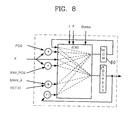
FIG. 8 is a block diagram of the A address generator 14 a. The A address generator 14 a is a block for generating an address for selecting the data output to BUSA in the register file (the data memory) 13. When the instruction word stored in the instruction register 11 is not for the matrix operation, the A address generator 14 a generates sixteen bit addresses obtained by linking the values stored in a BANK_A register for storing the high level addresses of data to the upper eight bit values of the IR register and outputs the generated sixteen bit addresses. When the instruction word stored in the instruction register 11 is for the matrix operation, the A address generator 14 a generates an address obtained by adding “POS” to “X” and the address obtained by adding 1 to the above address “POS”+“X”. When the obtained value is larger than “X”+“MAX_POS”, the “X” address is selected and output. Since it is necessary that a row be repeatedly selected in the case of matrix multiplication, the A address generator 14 a includes a register 80 for remembering a ROW address. I, J, and K values (here, I, J, and K denote the row of the resultant value, the column of the resultant value, and the index of the multiplication operation, respectively), which are inputs required for the matrix operation are reduced by one during the matrix operation. Only the “J” and “K” inputs are used in the A address generator 14 a.
FIG. 9 is a block diagram of the B address generator 14 b. The B address generator 14 b is a block for generating an address for selecting the data output to the BUSB in the register file (data memory) 13. The B address generator 14 b is different from the A address generator 14 a only in that a register for generating the “ROW” address is not included.
FIG. 10 is a block diagram of the C address generator 14 c. The C address generator 14 c is a block for generating an address for selecting the position of the data stored in the BUSC in the register file (the data memory) 13. The I, J, and K values are used in the C address generator. The values of “NUM_ROWS” and “NUM_COLS” registers for determining the sizes of the matrices are used in the C address generator 14 c. The values of the registers are required for performing instruction words (TRANSA) of exchanging the columns and the rows of the matrix and storing the exchanged columns and rows. This is because it is necessary to increase the address value by the number of columns (NUM_COLS). When the increased address value becomes larger than the maximum address value “X”+“MAX_POS”, “ADDRESS”+“NUM_ROWS”−“POS” is output. Since the C address generator 14 c generates an address in an EX state among the pipeline states shown in FIG. 15, the final output is generated two clock periods later than the addresses generated by the A address generator 14 a and the B address generator 14 b, which will be omitted in FIG. 10.
FIG. 11 shows instructions provided for the matrix operation in an embodiment of the digital signal processor according to the present invention shown in FIG. 1. The instructions support all types of matrix operations and data transmission between matrices and common data values.
Matrix operation instruction forms are shown in FIGS. 12A through 12K.
When “EXT” is at the head of an instruction word, the instruction word and the next instruction word linked thereto form one instruction word. Namely, LOADA and STOREA form a two-word instruction. However, ISMV and SETD form a two-word command or a single-word command.
The ISMV command stores immediate data in a specific register. When the required immediate data can be represented by eight bits, a single-word instruction is used. When a bit space greater than or equal to eight bits is necessary, a two-word instruction is used.
The SETD instruction determines the size required for the matrix operation. Matrix multiplication is represented by a two-word instruction since the I, J, and K values are required. A matrix addition is represented by a single-word instruction since only the I and J values are required.
The multiplication (MULTA) between matrices shown in FIG. 13A will now be described. Operands used in a 2×2 matrix multiplication stored in the data memory 13 of FIG. 1 are shown in FIG. 13B. The addresses of the matrix data X1, X2, and X3 stored in the matrix address storage means 22 of FIG. 1 are shown in FIG. 13C.
The operation state of the multiplication between the matrices shown in FIG. 13A can be represented as shown in FIG. 14. An embodiment of the digital signal processor according to the present invention is realized in the form of a pipeline. The operation of the multiplication between the matrices shown in FIG. 14 is performed for a time of nine clock periods. In FIG. 14, I and I′ represent a previous instruction word and an instruction word next to a MULTA instruction word. WE denotes a control signal for storing operation results in the register file (data memory) 13. Each address generator sequentially generates addresses to be suitable for the matrix operation.
FIG. 15 shows the pipeline structure of an embodiment of the digital signal processor according to the present invention in the order.
The instruction word stored in the program memory 10 IMEM is stored in the instruction register 11 IR (IF) (step 1,500). The output addresses of the register file (data memory) 13 are calculated by the above-mentioned method (AG) (step 1501). f(IR) and g(IR) denote the addresses generated by the A address generator 14 a and the B address generator 14 b, respectively. The values are the address values generated by “X”+“POS”. The data positioned in the generated addresses are moved to an operation block required by the register file (data memory) 13, that is, a multiplexer 15 d (OR) (step 1502). In FIG. 15, REGF denotes the data memory 13. Two data are multiplied with each other, and the address stored in the data memory 13 are calculated (EX) (step 1503). h(IR) denotes the address generated by the C address generator 14 c. The data obtained by performing an initial multiplication operation is not stored (step 1504).
The output addresses of the data memory are newly calculated and data items for the multiplication operation are moved to the multiplier 15 d (steps 1511 and 1512). The data items moved to the multiplier 15 d are multiplied with each other and the multiplication result MULT_C obtained in the step 1503 is added to an accumulated value (ACC) at the same time (step 1,513). When the operation of a row is completed, the accumulated value ACC is stored in the input address of the data memory 13 (WB) (step 1,514). Such operations are repeated until the matrix operation is completely performed.
After the multiplication operation is completed, the finally obtained multiplication result MULT_C is added to the accumulation value ACC and stored in the data memory 13 (steps 1523 and 1524). This series of operations is performed in a pipeline.
FIG. 16 compares the size of a program applied to a general digital signal processor with the size of a program applied to the digital signal processor according to the present invention. It is noted from FIG. 16 that the size of the program performed by the digital signal processor LP-DSP according to the present invention is smaller than the size of the program performed by a general digital signal processor G-DSP. The present invention can be more effectively used when the algorithm in which the matrix representation is effectively used is performed.
It is possible to more effectively program instruction words by the conventional signal processor by applying the present invention to an auditory digital hearing aid for which both low power consumption and small system size are essential. In order to verify the performance of the present invention, a printed circuit board (PCB) for a test is manufactured and a design using a field programmable gate array (FPGA) is completed. FIG. 17 shows a board for the test, which is designed by the above method. It is possible to note that the digital signal processor according to the present invention can perfectly perform given functions even though the program memory having the small capacity is included.
It is possible to reduce the size of the program memory in the digital signal processor by providing means for effectively representing the digital signal processing algorithm. Accordingly, it is possible to reduce the power consumption for reading the program memory, to thus operate electronic products for a long time.

Claims (17)

What is claimed is:
1. An apparatus included in a digital signal processor, for performing matrix operations, comprising:
a data storage means for storing operand data comprising matrix data in the form of a circular linked list and operation result data;
address generating means for sequentially generating addresses required for performing matrix operations, the address generating means comprising a matrix address storage means for storing, in the form of the circular linked list, addresses of the matrix data and outputting a first matrix data address, a second matrix data address, and an operation result matrix data address according to the contents of instruction words performed by the digital signal processor, wherein the sequentially generated addresses include a series of addresses of first operand data, a series of addresses of second operand data, and a series of stored addresses of operation result data that respectively correspond to the first, second and operating result matrix data addresses, whereby the addresses are sequentially generated according to contents of the instruction words; and
an operation means for reading data positioned in the address generated by the data storage means and performing operations according to the contents of the instruction words.
2. The apparatus of claim 1, wherein the address generating means further comprises:
an first address generator for receiving the first matrix data address from the matrix address storage means and sequentially generating the series of addresses of the first operand data according to the instruction words;
a second address generator for receiving the second matrix data address from the matrix address storage means and sequentially generating the series of addresses of the second operand data according to the instruction words; and
a third address generator for receiving the operation result matrix data address from the matrix address storage means and sequentially generating the series of stored addresses of the operation result data according to the instruction words.
3. The apparatus of claim 2, wherein the matrix address storage means comprises a plurality of matrix address register groups comprised of a first register for storing a memory address which shows the start of the circular linked list, a second register for storing a position value of currently processed data, which is a relative value with respect to the value stored in the first register, and a third register for storing the number of data items stored in the circular linked list.
4. The apparatus of claim 3, wherein the matrix address storage means further comprises a decoder for interpreting the address generated by the third address generator in order to determine the position in which the operation result obtained by the operation means is to be stored among the plurality of matrix address register groups.
5. The apparatus of claim 3, wherein the matrix address storage means further comprises a first multiplexer for selecting the first matrix data address according to the contents of the instruction words, a second multiplexer for selecting the second matrix data address according to the contents of the instruction words, and a third multiplexer for selecting the operation result matrix data address according to the contents of the instruction words, among the addresses of the matrix data stored in the plurality of matrix address register groups.
6. The apparatus of claim 3, wherein the first address generator receives the first matrix data address, adds the second register value to the first register value and outputs the addition result according to the instruction words, continuously outputs the address value obtained by adding 1 to the address value generated immediately prior, and lastly outputs the first register value when the address value is larger than the value obtained by adding the third register value to the first register value.
7. The apparatus of claim 2, wherein the first address generator comprises a register associated with a row address for outputting the same address value during a plurality of clock periods.
8. The apparatus of claim 2, wherein the first address generator comprises a scalar data generator for receiving an offset address included in the instruction words and the segment address of a segment address register, combining the segment address with the offset address, and outputting the combination result.
9. The apparatus of claim 3, wherein the second address generator receives the second matrix data address, adds the second register value to the first register value and outputs the addition result according to the instruction words, continuously outputs the address value obtained by adding 1 to the address value generated immediately prior, and lastly outputs the first register value when the address value is larger than the value obtained by adding the third register value to the first register value.
10. The apparatus of claim 2, wherein the second address generator comprises a scalar data generator for receiving an offset address included in the instruction words and the segment address of a segment address register, combining the segment address with the offset address, and outputting the combination result.
11. The apparatus of claim 3, wherein the third address generator receives the operation result matrix data address, adds the second register value to the first register value and outputs the addition result according to the instruction words, continuously outputs the address value obtained by adding 1 to the address value generated immediately prior, and lastly outputs the first register value when the address value is larger than the value obtained by adding the third register value to the first register value.
12. The apparatus of claim 3, wherein the third address generator receives a fourth register value and a fifth register value showing the size of the operation result matrix, outputs the address value obtained by adding the fifth register value to the address value generated immediately prior according to the instruction words, and outputs the address values obtained by adding the fourth register value to the address value generated immediately prior and subtracting the second register value from the address value generated immediately prior when the address value is larger than the value obtained by adding the third register value to the first register value.
13. The apparatus of claim 2, wherein the third address generator comprises a scalar data generator for receiving an offset address included in the instruction words and the segment address of a segment address register, combining the segment address with the offset address, and outputting the combination result.
14. The apparatus of claim 1, wherein the matrix address storage means comprises a plurality of matrix address register groups comprised of a first register for storing a memory address which shows the start of the circular linked list, a second register for storing the position value of currently processed data, which is a relative value with respect to the value stored in the first register, and a third register for storing the number of data items stored in the circular linked list.
15. The apparatus of claim 14, wherein the matrix address storage means further comprises a first multiplexer for selecting the first matrix data address according to the contents of the instruction words, a second multiplexer for selecting the second matrix data address according to the contents of the instruction words, and a third multiplexer for selecting the operation result matrix data address according to the contents of the instruction words, among the addresses of the matrix data stored in the plurality of matrix address register groups.
16. A digital signal processor capable of performing matrix operations, comprising:
a program memory for storing a signal processing program;
an instruction register for temporarily storing instruction words fetched by the program memory;
an instruction decoder for interpreting the instruction words stored in the instruction register and generating a control signal;
a data storage means for storing operand data including matrix data in the form of a circular linked list and operation result data;
an address generating means for sequentially generating, according to the control signal, a series of addresses of first operand data, a series of addresses of second operand data, and a series of stored addresses of operation result data for a matrix operation, wherein the address generating means comprises a matrix address storage means for storing, in the form of a circular linked list, addresses of the operand data and operation result data stored in the data storage means, and wherein each address of the first operand data, the second operand data and the operation result data corresponds to at least one data address stored in the matrix address storage means; and
an operation means for reading the data positioned at the address generated by the address generating means from the data storage means and performing operations according to the control signal.
17. A method of performing a matrix operation in the digital signal processor of claim 16, wherein the instruction decoder generates a control signal corresponding to a pipeline structure, the method comprising the steps of:
fetching the instruction words stored in the program memory and temporarily storing the fetched instruction words in the instruction register;
generating the addresses of the first operand data and the addresses of the second operand data by the address generating means;
reading the first operand data and the second operand data from the data storage means and moving the first operand data and the second operand data to the operation means;
performing operations by the operation means and generating the stored address of the operation result data by the address generating means; and
storing the operation result data output from the operation means in the data storage means.
US09/638,951 1999-12-17 2000-08-16 Matrix operation apparatus and digital signal processor capable of performing matrix operations Expired - Fee Related US6505288B1 (en)

Applications Claiming Priority (2)

Application Number Priority Date Filing Date Title
KR99-58763 1999-12-17
KR1019990058763A KR100331565B1 (en) 1999-12-17 1999-12-17 Matrix operation apparatus and Digital signal processor capable of matrix operation

Publications (1)

Publication Number Publication Date
US6505288B1 true US6505288B1 (en) 2003-01-07

Family

ID=19626741

Family Applications (1)

Application Number Title Priority Date Filing Date
US09/638,951 Expired - Fee Related US6505288B1 (en) 1999-12-17 2000-08-16 Matrix operation apparatus and digital signal processor capable of performing matrix operations

Country Status (3)

Country Link
US (1) US6505288B1 (en)
JP (1) JP3819686B2 (en)
KR (1) KR100331565B1 (en)

Cited By (15)

* Cited by examiner, † Cited by third party
Publication number Priority date Publication date Assignee Title
US20070050563A1 (en) * 2005-08-23 2007-03-01 Advanced Micro Devices, Inc. Synchronization arbiter for proactive synchronization within a multiprocessor computer system
US20080208942A1 (en) * 2007-02-23 2008-08-28 Nara Won Parallel Architecture for Matrix Transposition
US20100153648A1 (en) * 2008-12-16 2010-06-17 International Business Machines Corporation Block Driven Computation Using A Caching Policy Specified In An Operand Data Structure
US20100153931A1 (en) * 2008-12-16 2010-06-17 International Business Machines Corporation Operand Data Structure For Block Computation
US20100153681A1 (en) * 2008-12-16 2010-06-17 International Business Machines Corporation Block Driven Computation With An Address Generation Accelerator
US20100153683A1 (en) * 2008-12-16 2010-06-17 International Business Machines Corporation Specifying an Addressing Relationship In An Operand Data Structure
US20100153938A1 (en) * 2008-12-16 2010-06-17 International Business Machines Corporation Computation Table For Block Computation
US20100180100A1 (en) * 2009-01-13 2010-07-15 Mavrix Technology, Inc. Matrix microprocessor and method of operation
CN102629191A (en) * 2011-04-25 2012-08-08 中国电子科技集团公司第三十八研究所 Digital signal processor addressing method
CN102999476A (en) * 2011-09-09 2013-03-27 中国航天科工集团第三研究院第八三五七研究所 Two-dimensional matrix matching method and circuit
US20180004515A1 (en) * 2016-06-29 2018-01-04 Fujitsu Limited Processor and control method of processor
WO2018174930A1 (en) 2017-03-20 2018-09-27 Intel Corporation Systems, methods, and apparatuses for matrix add, subtract, and multiply
CN111857820A (en) * 2016-04-26 2020-10-30 中科寒武纪科技股份有限公司 Apparatus and method for performing matrix addition/subtraction operation
CN113836481A (en) * 2020-06-24 2021-12-24 北京希姆计算科技有限公司 Matrix calculation circuit, matrix calculation method, electronic device, and computer-readable storage medium
US11275588B2 (en) 2017-07-01 2022-03-15 Intel Corporation Context save with variable save state size

Families Citing this family (3)

* Cited by examiner, † Cited by third party
Publication number Priority date Publication date Assignee Title
JP4934356B2 (en) * 2006-06-20 2012-05-16 株式会社日立製作所 Video processing engine and video processing system including the same
KR101513954B1 (en) 2007-12-25 2015-04-21 히타치 긴조쿠 가부시키가이샤 Stacked inductor and power converter using the stacked inductor
CN112328960B (en) * 2020-11-02 2023-09-19 中国平安财产保险股份有限公司 Optimization method and device for data operation, electronic equipment and storage medium

Citations (10)

* Cited by examiner, † Cited by third party
Publication number Priority date Publication date Assignee Title
US3794984A (en) * 1971-10-14 1974-02-26 Raytheon Co Array processor for digital computers
US4150434A (en) * 1976-05-08 1979-04-17 Tokyo Shibaura Electric Co., Ltd. Matrix arithmetic apparatus
US4779192A (en) * 1983-12-23 1988-10-18 Hitachi, Ltd. Vector processor with a synchronously controlled operand fetch circuits
US4823258A (en) * 1982-02-26 1989-04-18 Tokyo Shibaura Denki Kabushiki Kaisha Index limited continuous operation vector processor
US5276819A (en) * 1987-05-01 1994-01-04 Hewlett-Packard Company Horizontal computer having register multiconnect for operand address generation during execution of iterations of a loop of program code
US5732251A (en) * 1996-05-06 1998-03-24 Advanced Micro Devices DSP with register file and multi-function instruction sequencer for vector processing by MACU
US6115812A (en) * 1998-04-01 2000-09-05 Intel Corporation Method and apparatus for efficient vertical SIMD computations
US6212618B1 (en) * 1998-03-31 2001-04-03 Intel Corporation Apparatus and method for performing multi-dimensional computations based on intra-add operation
US6314505B1 (en) * 1998-10-13 2001-11-06 Mitsubishi Denki Kabushiki Kaisha Processor and method for accessing rectangular areas in memory
US6332188B1 (en) * 1998-11-06 2001-12-18 Analog Devices, Inc. Digital signal processor with bit FIFO

Patent Citations (10)

* Cited by examiner, † Cited by third party
Publication number Priority date Publication date Assignee Title
US3794984A (en) * 1971-10-14 1974-02-26 Raytheon Co Array processor for digital computers
US4150434A (en) * 1976-05-08 1979-04-17 Tokyo Shibaura Electric Co., Ltd. Matrix arithmetic apparatus
US4823258A (en) * 1982-02-26 1989-04-18 Tokyo Shibaura Denki Kabushiki Kaisha Index limited continuous operation vector processor
US4779192A (en) * 1983-12-23 1988-10-18 Hitachi, Ltd. Vector processor with a synchronously controlled operand fetch circuits
US5276819A (en) * 1987-05-01 1994-01-04 Hewlett-Packard Company Horizontal computer having register multiconnect for operand address generation during execution of iterations of a loop of program code
US5732251A (en) * 1996-05-06 1998-03-24 Advanced Micro Devices DSP with register file and multi-function instruction sequencer for vector processing by MACU
US6212618B1 (en) * 1998-03-31 2001-04-03 Intel Corporation Apparatus and method for performing multi-dimensional computations based on intra-add operation
US6115812A (en) * 1998-04-01 2000-09-05 Intel Corporation Method and apparatus for efficient vertical SIMD computations
US6314505B1 (en) * 1998-10-13 2001-11-06 Mitsubishi Denki Kabushiki Kaisha Processor and method for accessing rectangular areas in memory
US6332188B1 (en) * 1998-11-06 2001-12-18 Analog Devices, Inc. Digital signal processor with bit FIFO

Non-Patent Citations (1)

* Cited by examiner, † Cited by third party
Title
Jang, Ho Rang et al., "A Digital Signal Processor For Low Power", AP-ASIC '99, The first IEEE Asia Pacific Conference on ASICs, Aug. 23-25, 1999, pp. 42-45.

Cited By (39)

* Cited by examiner, † Cited by third party
Publication number Priority date Publication date Assignee Title
US20070050563A1 (en) * 2005-08-23 2007-03-01 Advanced Micro Devices, Inc. Synchronization arbiter for proactive synchronization within a multiprocessor computer system
US7797362B2 (en) 2007-02-23 2010-09-14 Texas Instruments Incorporated Parallel architecture for matrix transposition
US20080208942A1 (en) * 2007-02-23 2008-08-28 Nara Won Parallel Architecture for Matrix Transposition
WO2008103885A2 (en) * 2007-02-23 2008-08-28 Texas Instruments Incorporated Parallel architecture for matrix transposition
WO2008103885A3 (en) * 2007-02-23 2008-10-16 Texas Instruments Inc Parallel architecture for matrix transposition
US8458439B2 (en) 2008-12-16 2013-06-04 International Business Machines Corporation Block driven computation using a caching policy specified in an operand data structure
US20100153648A1 (en) * 2008-12-16 2010-06-17 International Business Machines Corporation Block Driven Computation Using A Caching Policy Specified In An Operand Data Structure
US20100153683A1 (en) * 2008-12-16 2010-06-17 International Business Machines Corporation Specifying an Addressing Relationship In An Operand Data Structure
US20100153938A1 (en) * 2008-12-16 2010-06-17 International Business Machines Corporation Computation Table For Block Computation
WO2010069638A1 (en) * 2008-12-16 2010-06-24 International Business Machines Corporation Operand address generation
US20100153681A1 (en) * 2008-12-16 2010-06-17 International Business Machines Corporation Block Driven Computation With An Address Generation Accelerator
US20100153931A1 (en) * 2008-12-16 2010-06-17 International Business Machines Corporation Operand Data Structure For Block Computation
US8407680B2 (en) 2008-12-16 2013-03-26 International Business Machines Corporation Operand data structure for block computation
US8281106B2 (en) 2008-12-16 2012-10-02 International Business Machines Corporation Specifying an addressing relationship in an operand data structure
US8285971B2 (en) 2008-12-16 2012-10-09 International Business Machines Corporation Block driven computation with an address generation accelerator
US8327345B2 (en) 2008-12-16 2012-12-04 International Business Machines Corporation Computation table for block computation
US20100180100A1 (en) * 2009-01-13 2010-07-15 Mavrix Technology, Inc. Matrix microprocessor and method of operation
CN102629191A (en) * 2011-04-25 2012-08-08 中国电子科技集团公司第三十八研究所 Digital signal processor addressing method
CN102629191B (en) * 2011-04-25 2014-07-30 中国电子科技集团公司第三十八研究所 Digital signal processor addressing method
CN102999476A (en) * 2011-09-09 2013-03-27 中国航天科工集团第三研究院第八三五七研究所 Two-dimensional matrix matching method and circuit
CN102999476B (en) * 2011-09-09 2016-06-01 中国航天科工集团第三研究院第八三五七研究所 A kind of two-dimensional matrix matching process and circuit
CN111857820A (en) * 2016-04-26 2020-10-30 中科寒武纪科技股份有限公司 Apparatus and method for performing matrix addition/subtraction operation
EP3264261A3 (en) * 2016-06-29 2018-05-23 Fujitsu Limited Processor and control method of processor
US20180004515A1 (en) * 2016-06-29 2018-01-04 Fujitsu Limited Processor and control method of processor
US10754652B2 (en) * 2016-06-29 2020-08-25 Fujitsu Limited Processor and control method of processor for address generating and address displacement
US11567765B2 (en) 2017-03-20 2023-01-31 Intel Corporation Systems, methods, and apparatuses for tile load
WO2018174930A1 (en) 2017-03-20 2018-09-27 Intel Corporation Systems, methods, and apparatuses for matrix add, subtract, and multiply
US11163565B2 (en) 2017-03-20 2021-11-02 Intel Corporation Systems, methods, and apparatuses for dot production operations
US11200055B2 (en) 2017-03-20 2021-12-14 Intel Corporation Systems, methods, and apparatuses for matrix add, subtract, and multiply
US11847452B2 (en) 2017-03-20 2023-12-19 Intel Corporation Systems, methods, and apparatus for tile configuration
US11263008B2 (en) 2017-03-20 2022-03-01 Intel Corporation Systems, methods, and apparatuses for tile broadcast
US11714642B2 (en) 2017-03-20 2023-08-01 Intel Corporation Systems, methods, and apparatuses for tile store
US11288069B2 (en) 2017-03-20 2022-03-29 Intel Corporation Systems, methods, and apparatuses for tile store
US11288068B2 (en) 2017-03-20 2022-03-29 Intel Corporation Systems, methods, and apparatus for matrix move
US11360770B2 (en) 2017-03-20 2022-06-14 Intel Corporation Systems, methods, and apparatuses for zeroing a matrix
EP3602279A4 (en) * 2017-03-20 2021-03-31 Intel Corporation Systems, methods, and apparatuses for matrix add, subtract, and multiply
EP4137941A1 (en) * 2017-03-20 2023-02-22 Intel Corporation Systems, methods, and apparatuses for matrix add, subtract, and multiply
US11275588B2 (en) 2017-07-01 2022-03-15 Intel Corporation Context save with variable save state size
CN113836481A (en) * 2020-06-24 2021-12-24 北京希姆计算科技有限公司 Matrix calculation circuit, matrix calculation method, electronic device, and computer-readable storage medium

Also Published As

Publication number Publication date
JP2001184336A (en) 2001-07-06
KR20010078508A (en) 2001-08-21
JP3819686B2 (en) 2006-09-13
KR100331565B1 (en) 2002-04-06

Similar Documents

Publication Publication Date Title
US6505288B1 (en) Matrix operation apparatus and digital signal processor capable of performing matrix operations
EP3451162B1 (en) Device and method for use in executing matrix multiplication operations
US5880981A (en) Method and apparatus for reducing the power consumption in a programmable digital signal processor
US5859789A (en) Arithmetic unit
EP3910503A1 (en) Device and method for executing matrix addition/subtraction operation
CA1119731A (en) Multibus processor for increasing execution speed using a pipeline effect
US20080097625A1 (en) Iterative matrix processor based implementation of real-time model predictive control
US4539635A (en) Pipelined digital processor arranged for conditional operation
US5299144A (en) Architecture for covariance matrix generation
JPH02226420A (en) Floating point computation execution apparatus
US4598358A (en) Pipelined digital signal processor using a common data and control bus
US7555513B2 (en) SIMD processor having enhanced operand storage interconnects
EP1936492A1 (en) SIMD processor with reduction unit
US20030061468A1 (en) Forwarding the results of operations to dependent instructions quickly
US6996702B2 (en) Processing unit with cross-coupled ALUs/accumulators and input data feedback structure including constant generator and bypass to reduce memory contention
JP4979975B2 (en) Logic integrated circuit, source of arithmetic circuit, and computer-readable recording medium recording the source
US6792442B1 (en) Signal processor and product-sum operating device for use therein with rounding function
WO2008077803A1 (en) Simd processor with reduction unit
JP3723311B2 (en) Parallel processor
JP3547316B2 (en) Processor
JP2001034603A (en) Product-sum operation processor
JPH117440A (en) Processor, compiler, product-sum operation method and recording medium
JPH0744531A (en) Arithmetic device
JP2002182905A (en) Digital signal processing processor
JPH11203133A (en) Information processor

Legal Events

Date Code Title Description
AS Assignment

Owner name: SAMSUNG ELECTRONICS CO., LTD., KOREA, REPUBLIC OF

Free format text: ASSIGNMENT OF ASSIGNORS INTEREST;ASSIGNORS:JANG, HO-RANG;PARK, HYUN-WOO;CHO, JIN-CKUC;REEL/FRAME:011143/0358

Effective date: 20000829

FPAY Fee payment

Year of fee payment: 4

FEPP Fee payment procedure

Free format text: PAYOR NUMBER ASSIGNED (ORIGINAL EVENT CODE: ASPN); ENTITY STATUS OF PATENT OWNER: LARGE ENTITY

FPAY Fee payment

Year of fee payment: 8

REMI Maintenance fee reminder mailed
LAPS Lapse for failure to pay maintenance fees
STCH Information on status: patent discontinuation

Free format text: PATENT EXPIRED DUE TO NONPAYMENT OF MAINTENANCE FEES UNDER 37 CFR 1.362

FP Lapsed due to failure to pay maintenance fee

Effective date: 20150107