US6511884B1 - Method to form and/or isolate vertical transistors - Google Patents
Method to form and/or isolate vertical transistors Download PDFInfo
- Publication number
- US6511884B1 US6511884B1 US09/972,503 US97250301A US6511884B1 US 6511884 B1 US6511884 B1 US 6511884B1 US 97250301 A US97250301 A US 97250301A US 6511884 B1 US6511884 B1 US 6511884B1
- Authority
- US
- United States
- Prior art keywords
- wafer
- vertical pillar
- sti
- vertical
- oxide
- Prior art date
- Legal status (The legal status is an assumption and is not a legal conclusion. Google has not performed a legal analysis and makes no representation as to the accuracy of the status listed.)
- Expired - Lifetime
Links
- 238000000034 method Methods 0.000 title claims description 33
- 239000007943 implant Substances 0.000 claims abstract description 36
- 125000006850 spacer group Chemical group 0.000 claims abstract description 34
- 150000004767 nitrides Chemical class 0.000 claims abstract description 24
- 239000000463 material Substances 0.000 claims abstract description 12
- 238000004519 manufacturing process Methods 0.000 claims abstract description 10
- 230000015572 biosynthetic process Effects 0.000 claims abstract description 7
- XUIMIQQOPSSXEZ-UHFFFAOYSA-N Silicon Chemical compound [Si] XUIMIQQOPSSXEZ-UHFFFAOYSA-N 0.000 claims description 23
- 229910052710 silicon Inorganic materials 0.000 claims description 23
- 239000010703 silicon Substances 0.000 claims description 23
- 238000000059 patterning Methods 0.000 claims description 10
- 229910021420 polycrystalline silicon Inorganic materials 0.000 claims description 9
- 229920005591 polysilicon Polymers 0.000 claims description 9
- 238000000151 deposition Methods 0.000 claims description 5
- 238000005530 etching Methods 0.000 claims description 4
- 239000007791 liquid phase Substances 0.000 claims description 4
- 239000004065 semiconductor Substances 0.000 description 5
- 238000002955 isolation Methods 0.000 description 4
- 239000002019 doping agent Substances 0.000 description 2
- 238000000407 epitaxy Methods 0.000 description 2
- 230000005669 field effect Effects 0.000 description 2
- 230000000873 masking effect Effects 0.000 description 2
- 239000000758 substrate Substances 0.000 description 2
- 239000003990 capacitor Substances 0.000 description 1
- 230000015556 catabolic process Effects 0.000 description 1
- 238000007796 conventional method Methods 0.000 description 1
- 230000008021 deposition Effects 0.000 description 1
- 230000009977 dual effect Effects 0.000 description 1
- 238000002513 implantation Methods 0.000 description 1
- 229910044991 metal oxide Inorganic materials 0.000 description 1
- 150000004706 metal oxides Chemical class 0.000 description 1
- 230000003647 oxidation Effects 0.000 description 1
- 238000007254 oxidation reaction Methods 0.000 description 1
- 230000003071 parasitic effect Effects 0.000 description 1
- 239000010409 thin film Substances 0.000 description 1
Images


Classifications
-
- H—ELECTRICITY
- H01—ELECTRIC ELEMENTS
- H01L—SEMICONDUCTOR DEVICES NOT COVERED BY CLASS H10
- H01L29/00—Semiconductor devices adapted for rectifying, amplifying, oscillating or switching, or capacitors or resistors with at least one potential-jump barrier or surface barrier, e.g. PN junction depletion layer or carrier concentration layer; Details of semiconductor bodies or of electrodes thereof ; Multistep manufacturing processes therefor
- H01L29/66—Types of semiconductor device ; Multistep manufacturing processes therefor
- H01L29/66007—Multistep manufacturing processes
- H01L29/66075—Multistep manufacturing processes of devices having semiconductor bodies comprising group 14 or group 13/15 materials
- H01L29/66227—Multistep manufacturing processes of devices having semiconductor bodies comprising group 14 or group 13/15 materials the devices being controllable only by the electric current supplied or the electric potential applied, to an electrode which does not carry the current to be rectified, amplified or switched, e.g. three-terminal devices
- H01L29/66409—Unipolar field-effect transistors
- H01L29/66477—Unipolar field-effect transistors with an insulated gate, i.e. MISFET
- H01L29/66666—Vertical transistors
-
- H—ELECTRICITY
- H01—ELECTRIC ELEMENTS
- H01L—SEMICONDUCTOR DEVICES NOT COVERED BY CLASS H10
- H01L29/00—Semiconductor devices adapted for rectifying, amplifying, oscillating or switching, or capacitors or resistors with at least one potential-jump barrier or surface barrier, e.g. PN junction depletion layer or carrier concentration layer; Details of semiconductor bodies or of electrodes thereof ; Multistep manufacturing processes therefor
- H01L29/66—Types of semiconductor device ; Multistep manufacturing processes therefor
- H01L29/68—Types of semiconductor device ; Multistep manufacturing processes therefor controllable by only the electric current supplied, or only the electric potential applied, to an electrode which does not carry the current to be rectified, amplified or switched
- H01L29/76—Unipolar devices, e.g. field effect transistors
- H01L29/772—Field effect transistors
- H01L29/78—Field effect transistors with field effect produced by an insulated gate
- H01L29/7827—Vertical transistors
Definitions
- the present invention relates generally to fabrication of semiconductor devices, and more specifically to methods of fabricating vertical transistors.
- U.S. Pat. No. 5,429,977 to Lu et al. describes a method for forming a vertical transistor with a stacked capacitor DRAM (dynamic random access memory) cell.
- Another object of the present invention is to provide an improved method of isolating vertical transistors in combination with the fabrication of those vertical transistors.
- a wafer having a first implanted region selected from the group comprising a source region and a drain region is provided.
- the wafer further includes STI areas on either side of a center transistor area.
- the wafer is patterned down to the first implanted region to form a vertical, pillar within the center transistor area using a patterned hardmask.
- the vertical pillar having side walls.
- a pad dielectric layer is formed over the wafer, lining the vertical pillar.
- a nitride layer is formed over the pad dielectric layer.
- the structure is patterned and etched through the nitride layer and the pad dielectric layer; and into the wafer within the STI areas to form STI trenches within the wafer.
- the STI trenches are filled with insulative material to form STIs within STI trenches.
- the patterned nitride and pad dielectric layers are removed.
- the patterned hardmask is removed.
- Gate oxide is grown over the exposed portions of the wafer and the vertical pillar. Spacer gates are formed over the gate oxide lined side walls of the vertical pillar.
- Spacer gate implants are formed within the spacer gates, and a second implanted region is formed within the vertical pillar selected from the group consisting of a drain region and a source region that is not the same as the first implanted region to complete formation of the isolated vertical transistor.
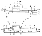
- FIGS. 1 to 9 schematically illustrate in cross-sectional representation a preferred embodiment of the present invention.
- FIG. 1 illustrates a cross-sectional view of a wafer 10 , preferably a semiconductor silicon wafer, after masking (not shown) and implantation of source and well regions/source level (N + /P + ) 12 deep in the Si wafer 10 .
- Si wafer 10 further includes STI areas 11 (designating the location of STIs 24 to be formed) adjacent a central transistor area 15 (designating the location of a vertical transistor 40 to be formed).
- patterned hardmask 14 is formed over Si wafer 10 where a vertical pillar(s) is/are desired.
- Hardmask 14 is preferably comprised of silicon oxynitride.
- Si wafer 10 not under patterned hardmask 14 is etched, stopping at N + /P + source regions/level 12 .
- thin pad dielectric 18 preferably a thin pad oxide, is deposited over Si wafer 10 and over vertical Si pillar 16 and patterned hardmask 14 .
- Nitride layer 20 is then deposited over thin pad oxide 18 .
- Layer 20 may also be formed of resist in which case the resist layer 20 is exposed and developed instead of being etched.
- nitride layer 20 is patterned and etched, with the etch continuing through thin pad oxide 18 and into Si wafer 10 to form shallow trench isolation (STI) trenches 22 at either side of vertical Si pillar 16 , to isolate vertical Si pillar 16 and thus the subsequently finished vertical transistor 40 .
- STI shallow trench isolation
- This method allows the vertical transistor 40 to stick up above the top of the STI 24 without requiring the use of selective epitaxy.
- STI trenches 22 are then filled with an insulative material, preferably by and with a liquid phase deposited oxide, to form STI's 24 .
- patterned nitride layer 20 ′ and thin pad oxide 18 ′ are removed from the structure.
- patterned hardmask 14 is removed from vertical Si pillar 16 .
- the structure is masked (not shown) and well implants 28 and threshold-voltage (V t ) adjust implants (not shown) are performed as at 26 and 27 , respectively.
- the threshold-voltage (V t ) adjust implants form the channel (not shown).
- One mask is used to form a P-type adjust implant and an N-type threshold-voltage (V t ) adjust implant.
- gate oxide 30 is grown over the exposed portions of silicon (Si) over Si wafer 10 and the side walls and top of vertical Si pillar 16 .
- spacer gate (vertical gate) 32 are formed over gate oxide lined side walls of vertical Si pillar 16 proximate the channel(s) (not shown), preferably by depositing polysilicon (poly), patterning the poly and etching gate to form poly spacer gates 32 .
- the vertical area adjacent spacer gate 32 are channels. This is necessary to define poly lines for connecting gates together or for forming contact landing pads.
- the structure is masked (not shown) and drain 36 and spacer gate 32 implants are performed preferably at a small tilt angle as at 34 , rotating all around vertical Si pillar 16 .
- the poly gates are doped at the same time.
- the dopants are activated and further processing may be done.
- the present invention may also be practiced without STIs is some other means of isolation is used such as junction isolation (high parasitic capacitance and low junction breakdowns) or LOCOS (needs high temperature oxidation).
- Another way of forming the vertical transistor would have the source regions implanted at the same time as the drain (after STI formation). This would eliminate the need for the buried N + or P + layer 12 . This would also give better transistor characteristics as the height of the transistor pillar (channel length) is scaled down.
Abstract
Description
Claims (27)
Priority Applications (2)
| Application Number | Priority Date | Filing Date | Title |
|---|---|---|---|
| US09/972,503 US6511884B1 (en) | 2001-10-09 | 2001-10-09 | Method to form and/or isolate vertical transistors |
| SG200205417A SG103360A1 (en) | 2001-10-09 | 2002-09-06 | A method to form and/or isolate vertical transistors |
Applications Claiming Priority (1)
| Application Number | Priority Date | Filing Date | Title |
|---|---|---|---|
| US09/972,503 US6511884B1 (en) | 2001-10-09 | 2001-10-09 | Method to form and/or isolate vertical transistors |
Publications (1)
| Publication Number | Publication Date |
|---|---|
| US6511884B1 true US6511884B1 (en) | 2003-01-28 |
Family
ID=25519726
Family Applications (1)
| Application Number | Title | Priority Date | Filing Date |
|---|---|---|---|
| US09/972,503 Expired - Lifetime US6511884B1 (en) | 2001-10-09 | 2001-10-09 | Method to form and/or isolate vertical transistors |
Country Status (2)
| Country | Link |
|---|---|
| US (1) | US6511884B1 (en) |
| SG (1) | SG103360A1 (en) |
Cited By (14)
| Publication number | Priority date | Publication date | Assignee | Title |
|---|---|---|---|---|
| US20040052139A1 (en) * | 2002-06-21 | 2004-03-18 | Brown Kris K. | Memory cell and method for forming the same |
| US20040183567A1 (en) * | 2003-03-20 | 2004-09-23 | Engler David W. | Isolated channel in an integrated circuit |
| US20050063233A1 (en) * | 2002-06-21 | 2005-03-24 | Brown Kris K. | Memory cell and method for forming the same |
| US20050124120A1 (en) * | 2003-12-05 | 2005-06-09 | Yang Du | Method and circuit for multiplying signals with a transistor having more than one independent gate structure |
| US20050130387A1 (en) * | 2003-12-11 | 2005-06-16 | International Business Machines Corporation | Shallow trench isolation fill by liquid phase deposition of SiO2 |
| US20050275037A1 (en) * | 2004-06-12 | 2005-12-15 | Chung Shine C | Semiconductor devices with high voltage tolerance |
| US20060220086A1 (en) * | 2005-03-30 | 2006-10-05 | Stmicroelectronics Crolles 2 Sas | IMOS transistor |
| US20060223257A1 (en) * | 2002-08-14 | 2006-10-05 | Advanced Analogic Technologies, Inc. | Method Of Fabricating Isolated Semiconductor Devices In Epi-Less Substrate |
| US20060249776A1 (en) * | 2005-05-05 | 2006-11-09 | Manning H M | Memory cell, device, system and method for forming same |
| US20080040696A1 (en) * | 2003-12-11 | 2008-02-14 | International Business Machines Corporation | Design Structures Incorporating Shallow Trench Isolation Filled by Liquid Phase Deposition of SiO2 |
| US20100187600A1 (en) * | 2008-02-15 | 2010-07-29 | Unisantis Electronics (Japan) Ltd. | Semiconductor device and method of producing the same |
| US8241976B2 (en) | 2008-02-15 | 2012-08-14 | Unisantis Electronics Singapore Pte Ltd. | Semiconductor surrounding gate transistor device and production method therefor |
| TWI423344B (en) * | 2008-02-15 | 2014-01-11 | Unisantis Elect Singapore Pte | Semiconductor device and method of producing the same |
| CN103633140A (en) * | 2012-08-24 | 2014-03-12 | 台湾积体电路制造股份有限公司 | Two-step shallow trench isolation (STI) process |
Citations (7)
| Publication number | Priority date | Publication date | Assignee | Title |
|---|---|---|---|---|
| US5312767A (en) | 1989-12-15 | 1994-05-17 | Mitsubishi Denki Kabushiki Kaisha | MOS type field effect transistor and manufacturing method thereof |
| US5413948A (en) | 1993-01-19 | 1995-05-09 | Motorola, Inc. | Method for forming a dual transistor structure |
| US5429977A (en) | 1994-03-11 | 1995-07-04 | Industrial Technology Research Institute | Method for forming a vertical transistor with a stacked capacitor DRAM cell |
| US5670810A (en) | 1994-08-25 | 1997-09-23 | Matsushita Electric Industrial Co., Ltd. | Semiconductor device with a vertical field effect transistor |
| US5693549A (en) | 1994-09-13 | 1997-12-02 | Lg Semicon Co., Ltd. | Method of fabricating thin film transistor with supplementary gates |
| US5773343A (en) | 1995-05-12 | 1998-06-30 | Lg Semicon Co., Ltd. | Semiconductor device having a recessed channel structure and method for fabricating the same |
| US6069384A (en) | 1997-03-04 | 2000-05-30 | Advanced Micro Devices, Inc. | Integrated circuit including vertical transistors with spacer gates having selected gate widths |
-
2001
- 2001-10-09 US US09/972,503 patent/US6511884B1/en not_active Expired - Lifetime
-
2002
- 2002-09-06 SG SG200205417A patent/SG103360A1/en unknown
Patent Citations (7)
| Publication number | Priority date | Publication date | Assignee | Title |
|---|---|---|---|---|
| US5312767A (en) | 1989-12-15 | 1994-05-17 | Mitsubishi Denki Kabushiki Kaisha | MOS type field effect transistor and manufacturing method thereof |
| US5413948A (en) | 1993-01-19 | 1995-05-09 | Motorola, Inc. | Method for forming a dual transistor structure |
| US5429977A (en) | 1994-03-11 | 1995-07-04 | Industrial Technology Research Institute | Method for forming a vertical transistor with a stacked capacitor DRAM cell |
| US5670810A (en) | 1994-08-25 | 1997-09-23 | Matsushita Electric Industrial Co., Ltd. | Semiconductor device with a vertical field effect transistor |
| US5693549A (en) | 1994-09-13 | 1997-12-02 | Lg Semicon Co., Ltd. | Method of fabricating thin film transistor with supplementary gates |
| US5773343A (en) | 1995-05-12 | 1998-06-30 | Lg Semicon Co., Ltd. | Semiconductor device having a recessed channel structure and method for fabricating the same |
| US6069384A (en) | 1997-03-04 | 2000-05-30 | Advanced Micro Devices, Inc. | Integrated circuit including vertical transistors with spacer gates having selected gate widths |
Cited By (48)
| Publication number | Priority date | Publication date | Assignee | Title |
|---|---|---|---|---|
| US6921935B2 (en) | 2002-06-21 | 2005-07-26 | Micron Technology, Inc. | Memory cell and method for forming the same |
| US7176513B2 (en) | 2002-06-21 | 2007-02-13 | Micron Technology, Inc. | Memory cell and method for forming the same |
| US20040052139A1 (en) * | 2002-06-21 | 2004-03-18 | Brown Kris K. | Memory cell and method for forming the same |
| US6797573B2 (en) | 2002-06-21 | 2004-09-28 | Micron Technology, Inc. | Memory cell and method for forming the same |
| US20040219742A1 (en) * | 2002-06-21 | 2004-11-04 | Brown Kris K. | Memory cell and method for forming the same |
| US20050063233A1 (en) * | 2002-06-21 | 2005-03-24 | Brown Kris K. | Memory cell and method for forming the same |
| US20050082594A1 (en) * | 2002-06-21 | 2005-04-21 | Brown Kris K. | Memory cell and method for forming the same |
| US20050082588A1 (en) * | 2002-06-21 | 2005-04-21 | Brown Kris K. | Memory cell and method for forming the same |
| US7276418B2 (en) | 2002-06-21 | 2007-10-02 | Micron Technology, Inc. | Memory cell and method for forming the same |
| US7324367B2 (en) | 2002-06-21 | 2008-01-29 | Micron Technology, Inc. | Memory cell and method for forming the same |
| US20080099816A1 (en) * | 2002-06-21 | 2008-05-01 | Brown Kris K | Memory cell and method for forming the same |
| US6756625B2 (en) | 2002-06-21 | 2004-06-29 | Micron Technology, Inc. | Memory cell and method for forming the same |
| US7518174B2 (en) | 2002-06-21 | 2009-04-14 | Micron Technology, Inc. | Memory cell and method for forming the same |
| US7045844B2 (en) | 2002-06-21 | 2006-05-16 | Micron Technology, Inc. | Memory cell and method for forming the same |
| US20060063330A1 (en) * | 2002-06-21 | 2006-03-23 | Brown Kris K | Memory cell and method for forming the same |
| US20060068548A1 (en) * | 2002-06-21 | 2006-03-30 | Brown Kris K | Memory cell and method for forming the same |
| US7034351B2 (en) | 2002-06-21 | 2006-04-25 | Micron Technology, Inc. | Memory cell and method for forming the same |
| US7445979B2 (en) * | 2002-08-14 | 2008-11-04 | Advanced Analogic Technologies, Inc. | Method of fabricating isolated semiconductor devices in epi-less substrate |
| US20060223257A1 (en) * | 2002-08-14 | 2006-10-05 | Advanced Analogic Technologies, Inc. | Method Of Fabricating Isolated Semiconductor Devices In Epi-Less Substrate |
| US20040183567A1 (en) * | 2003-03-20 | 2004-09-23 | Engler David W. | Isolated channel in an integrated circuit |
| US6975136B2 (en) * | 2003-03-20 | 2005-12-13 | Hewlett-Packard Development Company, L.P. | Isolated channel in an integrated circuit |
| US20050124120A1 (en) * | 2003-12-05 | 2005-06-09 | Yang Du | Method and circuit for multiplying signals with a transistor having more than one independent gate structure |
| US6969656B2 (en) * | 2003-12-05 | 2005-11-29 | Freescale Semiconductor, Inc. | Method and circuit for multiplying signals with a transistor having more than one independent gate structure |
| US7273794B2 (en) * | 2003-12-11 | 2007-09-25 | International Business Machines Corporation | Shallow trench isolation fill by liquid phase deposition of SiO2 |
| US20050130387A1 (en) * | 2003-12-11 | 2005-06-16 | International Business Machines Corporation | Shallow trench isolation fill by liquid phase deposition of SiO2 |
| US20070228510A1 (en) * | 2003-12-11 | 2007-10-04 | International Business Machines Corporation | SHALLOW TRENCH ISOLATION FILL BY LIQUID PHASE DEPOSITION OF SiO2 |
| US20080040696A1 (en) * | 2003-12-11 | 2008-02-14 | International Business Machines Corporation | Design Structures Incorporating Shallow Trench Isolation Filled by Liquid Phase Deposition of SiO2 |
| US7525156B2 (en) | 2003-12-11 | 2009-04-28 | International Business Machines Corporation | Shallow trench isolation fill by liquid phase deposition of SiO2 |
| US20080197448A1 (en) * | 2003-12-11 | 2008-08-21 | International Business Machines Corporation | SHALLOW TRENCH ISOLATION FILL BY LIQUID PHASE DEPOSITION OF SiO2 |
| US20050275037A1 (en) * | 2004-06-12 | 2005-12-15 | Chung Shine C | Semiconductor devices with high voltage tolerance |
| US7608867B2 (en) | 2005-03-30 | 2009-10-27 | Stmicroelectronics Crolles 2 Sas | Vertical IMOS transistor having a PIN diode formed within |
| FR2884052A1 (en) * | 2005-03-30 | 2006-10-06 | St Microelectronics Crolles 2 | Vertical impact ionization metal oxide semiconductor transistor for use as e.g. N-channel MOS transistor, has stack with semiconductor portions to form vertical PIN type diode, and gate, placed against stack, with thickness less than stack |
| US20060220086A1 (en) * | 2005-03-30 | 2006-10-05 | Stmicroelectronics Crolles 2 Sas | IMOS transistor |
| US20090173982A1 (en) * | 2005-05-05 | 2009-07-09 | Micron Technology, Inc. | Method for forming memory cell and device |
| US20100290268A1 (en) * | 2005-05-05 | 2010-11-18 | Micron Technology, Inc. | Memory cell, pair of memory cells, and memory array |
| US7372092B2 (en) | 2005-05-05 | 2008-05-13 | Micron Technology, Inc. | Memory cell, device, and system |
| US20070173014A1 (en) * | 2005-05-05 | 2007-07-26 | Manning H M | Method for forming memory cell and device |
| US20060249776A1 (en) * | 2005-05-05 | 2006-11-09 | Manning H M | Memory cell, device, system and method for forming same |
| US8207564B2 (en) | 2005-05-05 | 2012-06-26 | Micron Technology, Inc. | Memory cell, pair of memory cells, and memory array |
| US7786522B2 (en) | 2005-05-05 | 2010-08-31 | Micron Technology, Inc. | Method for forming memory cell and device |
| US7504298B2 (en) | 2005-05-05 | 2009-03-17 | Micron Technology, Inc. | Method for forming memory cell and device |
| US20100187600A1 (en) * | 2008-02-15 | 2010-07-29 | Unisantis Electronics (Japan) Ltd. | Semiconductor device and method of producing the same |
| US8211758B2 (en) * | 2008-02-15 | 2012-07-03 | Unisantis Electronics Singapore Pte Ltd. | Semiconductor device and method of producing the same |
| US8241976B2 (en) | 2008-02-15 | 2012-08-14 | Unisantis Electronics Singapore Pte Ltd. | Semiconductor surrounding gate transistor device and production method therefor |
| US8395208B2 (en) | 2008-02-15 | 2013-03-12 | Unisantis Electronics Singapore Pte Ltd. | Semiconductor device and method of producing the same |
| TWI423344B (en) * | 2008-02-15 | 2014-01-11 | Unisantis Elect Singapore Pte | Semiconductor device and method of producing the same |
| CN103633140A (en) * | 2012-08-24 | 2014-03-12 | 台湾积体电路制造股份有限公司 | Two-step shallow trench isolation (STI) process |
| CN103633140B (en) * | 2012-08-24 | 2016-06-01 | 台湾积体电路制造股份有限公司 | Dual-step type shallow trench isolation is from (STI) technique |
Also Published As
| Publication number | Publication date |
|---|---|
| SG103360A1 (en) | 2004-04-29 |
Similar Documents
| Publication | Publication Date | Title |
|---|---|---|
| US6624032B2 (en) | Structure and process flow for fabrication of dual gate floating body integrated MOS transistors | |
| JP5137310B2 (en) | Structure including trench capacitor array and method of forming the same (simplified buried plate structure and process for SOI chip) | |
| US4835115A (en) | Method for forming oxide-capped trench isolation | |
| US5869868A (en) | SOI trench DRAM cell for 256 MB DRAM and beyond | |
| KR100745518B1 (en) | Cmos well structure and method of forming the same | |
| US6448124B1 (en) | Method for epitaxial bipolar BiCMOS | |
| US6406962B1 (en) | Vertical trench-formed dual-gate FET device structure and method for creation | |
| US4980747A (en) | Deep trench isolation with surface contact to substrate | |
| US6309919B1 (en) | Method for fabricating a trench-gated vertical CMOS device | |
| US5795801A (en) | MethodS of fabricating profiled device wells for improved device isolation | |
| KR100354119B1 (en) | A disposable-spacer damascene-gate process for sub 0.05㎛ mos devices | |
| US5292683A (en) | Method of isolating semiconductor devices and arrays of memory integrated circuitry | |
| US20070057288A1 (en) | Methods of Fabricating Semiconductor Devices with Enlarged Recessed Gate Electrodes | |
| US5106777A (en) | Trench isolation process with reduced topography | |
| US6511884B1 (en) | Method to form and/or isolate vertical transistors | |
| US20120112309A1 (en) | Low cost fabrication of double box back gate silicon-on-insulator wafers with subsequent self aligned shallow trench isolation | |
| KR20030032836A (en) | A method to form a self-aligned CMOS inverter using vertical device integration | |
| JPH1050863A (en) | Mos transistor and its manufacturing method | |
| JPH11274496A (en) | Field-effect transistor having improved implant and its manufacture | |
| US6844223B2 (en) | Semiconductor device having silicon on insulator and fabricating method therefor | |
| US6800921B1 (en) | Method of fabricating a polysilicon capacitor utilizing fet and bipolar base polysilicon layers | |
| US5742090A (en) | Narrow width trenches for field isolation in integrated circuits | |
| KR100507856B1 (en) | Method for fabricating MOS transistor | |
| US7670926B2 (en) | Method for forming shallow trench isolation utilizing two filling oxide layers | |
| US5179038A (en) | High density trench isolation for MOS circuits |
Legal Events
| Date | Code | Title | Description |
|---|---|---|---|
| AS | Assignment |
Owner name: CHARTERED SEMICONDUCTOR MANUFACTURING LTD., SINGAP Free format text: ASSIGNMENT OF ASSIGNORS INTEREST;ASSIGNORS:QUEK, ELGIN;SUNDARESAN, RAVI;PAN, YANG;AND OTHERS;REEL/FRAME:012240/0051 Effective date: 20010912 |
|
| AS | Assignment |
Owner name: CHARTERED SEMICONDUCTOR MANUFACTURING LTD., SINGAP Free format text: CORRECTIVE ASSIGNMENT TO CORRECT THE NAME OF CONVEYING PARTY THAT WAS PREVIOUSLY RECORDED ON REEL 012240, FRAME 0051;ASSIGNORS:QUEK, ELGIN;SUNDARESAN, RAVI;PAN, YANG;AND OTHERS;REEL/FRAME:013093/0642 Effective date: 20010912 |
|
| STCF | Information on status: patent grant |
Free format text: PATENTED CASE |
|
| CC | Certificate of correction | ||
| FPAY | Fee payment |
Year of fee payment: 4 |
|
| REFU | Refund |
Free format text: REFUND - 7.5 YR SURCHARGE - LATE PMT W/IN 6 MO, LARGE ENTITY (ORIGINAL EVENT CODE: R1555); ENTITY STATUS OF PATENT OWNER: LARGE ENTITY Free format text: REFUND - PAYMENT OF MAINTENANCE FEE, 8TH YEAR, LARGE ENTITY (ORIGINAL EVENT CODE: R1552); ENTITY STATUS OF PATENT OWNER: LARGE ENTITY |
|
| FPAY | Fee payment |
Year of fee payment: 8 |
|
| SULP | Surcharge for late payment |
Year of fee payment: 7 |
|
| FPAY | Fee payment |
Year of fee payment: 12 |