US6520109B2 - Heat insulation arrangement of indicating instrument - Google Patents
Heat insulation arrangement of indicating instrument Download PDFInfo
- Publication number
- US6520109B2 US6520109B2 US09/816,143 US81614301A US6520109B2 US 6520109 B2 US6520109 B2 US 6520109B2 US 81614301 A US81614301 A US 81614301A US 6520109 B2 US6520109 B2 US 6520109B2
- Authority
- US
- United States
- Prior art keywords
- circuit board
- light emitting
- printed circuit
- emitting diode
- lead wires
- Prior art date
- Legal status (The legal status is an assumption and is not a legal conclusion. Google has not performed a legal analysis and makes no representation as to the accuracy of the status listed.)
- Expired - Lifetime, expires
Links
- 238000009413 insulation Methods 0.000 title description 4
- 238000005476 soldering Methods 0.000 claims abstract description 25
- WABPQHHGFIMREM-UHFFFAOYSA-N lead(0) Chemical compound [Pb] WABPQHHGFIMREM-UHFFFAOYSA-N 0.000 claims description 40
- 230000008642 heat stress Effects 0.000 description 4
- 238000000034 method Methods 0.000 description 4
- 230000035939 shock Effects 0.000 description 4
- 230000035882 stress Effects 0.000 description 4
- 238000005286 illumination Methods 0.000 description 3
- RYGMFSIKBFXOCR-UHFFFAOYSA-N Copper Chemical compound [Cu] RYGMFSIKBFXOCR-UHFFFAOYSA-N 0.000 description 1
- 239000004642 Polyimide Substances 0.000 description 1
- XAGFODPZIPBFFR-UHFFFAOYSA-N aluminium Chemical compound [Al] XAGFODPZIPBFFR-UHFFFAOYSA-N 0.000 description 1
- 229910052782 aluminium Inorganic materials 0.000 description 1
- 229910052802 copper Inorganic materials 0.000 description 1
- 239000010949 copper Substances 0.000 description 1
- 238000012986 modification Methods 0.000 description 1
- 230000004048 modification Effects 0.000 description 1
- 229920003055 poly(ester-imide) Polymers 0.000 description 1
- 229920001721 polyimide Polymers 0.000 description 1
- 229910000679 solder Inorganic materials 0.000 description 1
- 239000007787 solid Substances 0.000 description 1
Images


Classifications
-
- G—PHYSICS
- G01—MEASURING; TESTING
- G01D—MEASURING NOT SPECIALLY ADAPTED FOR A SPECIFIC VARIABLE; ARRANGEMENTS FOR MEASURING TWO OR MORE VARIABLES NOT COVERED IN A SINGLE OTHER SUBCLASS; TARIFF METERING APPARATUS; MEASURING OR TESTING NOT OTHERWISE PROVIDED FOR
- G01D13/00—Component parts of indicators for measuring arrangements not specially adapted for a specific variable
- G01D13/22—Pointers, e.g. settable pointer
- G01D13/28—Pointers, e.g. settable pointer with luminescent markings
-
- H—ELECTRICITY
- H05—ELECTRIC TECHNIQUES NOT OTHERWISE PROVIDED FOR
- H05K—PRINTED CIRCUITS; CASINGS OR CONSTRUCTIONAL DETAILS OF ELECTRIC APPARATUS; MANUFACTURE OF ASSEMBLAGES OF ELECTRICAL COMPONENTS
- H05K1/00—Printed circuits
- H05K1/18—Printed circuits structurally associated with non-printed electric components
-
- G—PHYSICS
- G01—MEASURING; TESTING
- G01D—MEASURING NOT SPECIALLY ADAPTED FOR A SPECIFIC VARIABLE; ARRANGEMENTS FOR MEASURING TWO OR MORE VARIABLES NOT COVERED IN A SINGLE OTHER SUBCLASS; TARIFF METERING APPARATUS; MEASURING OR TESTING NOT OTHERWISE PROVIDED FOR
- G01D3/00—Indicating or recording apparatus with provision for the special purposes referred to in the subgroups
- G01D3/08—Indicating or recording apparatus with provision for the special purposes referred to in the subgroups with provision for safeguarding the apparatus, e.g. against abnormal operation, against breakdown
-
- H—ELECTRICITY
- H02—GENERATION; CONVERSION OR DISTRIBUTION OF ELECTRIC POWER
- H02K—DYNAMO-ELECTRIC MACHINES
- H02K5/00—Casings; Enclosures; Supports
- H02K5/04—Casings or enclosures characterised by the shape, form or construction thereof
- H02K5/22—Auxiliary parts of casings not covered by groups H02K5/06-H02K5/20, e.g. shaped to form connection boxes or terminal boxes
- H02K5/225—Terminal boxes or connection arrangements
-
- B60K2360/698—
-
- H—ELECTRICITY
- H02—GENERATION; CONVERSION OR DISTRIBUTION OF ELECTRIC POWER
- H02K—DYNAMO-ELECTRIC MACHINES
- H02K2203/00—Specific aspects not provided for in the other groups of this subclass relating to the windings
- H02K2203/03—Machines characterised by the wiring boards, i.e. printed circuit boards or similar structures for connecting the winding terminations
-
- H—ELECTRICITY
- H02—GENERATION; CONVERSION OR DISTRIBUTION OF ELECTRIC POWER
- H02K—DYNAMO-ELECTRIC MACHINES
- H02K2211/00—Specific aspects not provided for in the other groups of this subclass relating to measuring or protective devices or electric components
- H02K2211/03—Machines characterised by circuit boards, e.g. pcb
-
- H—ELECTRICITY
- H05—ELECTRIC TECHNIQUES NOT OTHERWISE PROVIDED FOR
- H05K—PRINTED CIRCUITS; CASINGS OR CONSTRUCTIONAL DETAILS OF ELECTRIC APPARATUS; MANUFACTURE OF ASSEMBLAGES OF ELECTRICAL COMPONENTS
- H05K2201/00—Indexing scheme relating to printed circuits covered by H05K1/00
- H05K2201/09—Shape and layout
- H05K2201/09818—Shape or layout details not covered by a single group of H05K2201/09009 - H05K2201/09809
- H05K2201/09972—Partitioned, e.g. portions of a PCB dedicated to different functions; Boundary lines therefore; Portions of a PCB being processed separately or differently
-
- H—ELECTRICITY
- H05—ELECTRIC TECHNIQUES NOT OTHERWISE PROVIDED FOR
- H05K—PRINTED CIRCUITS; CASINGS OR CONSTRUCTIONAL DETAILS OF ELECTRIC APPARATUS; MANUFACTURE OF ASSEMBLAGES OF ELECTRICAL COMPONENTS
- H05K2201/00—Indexing scheme relating to printed circuits covered by H05K1/00
- H05K2201/10—Details of components or other objects attached to or integrated in a printed circuit board
- H05K2201/10007—Types of components
- H05K2201/1009—Electromotor
-
- H—ELECTRICITY
- H05—ELECTRIC TECHNIQUES NOT OTHERWISE PROVIDED FOR
- H05K—PRINTED CIRCUITS; CASINGS OR CONSTRUCTIONAL DETAILS OF ELECTRIC APPARATUS; MANUFACTURE OF ASSEMBLAGES OF ELECTRICAL COMPONENTS
- H05K2201/00—Indexing scheme relating to printed circuits covered by H05K1/00
- H05K2201/10—Details of components or other objects attached to or integrated in a printed circuit board
- H05K2201/10007—Types of components
- H05K2201/10106—Light emitting diode [LED]
-
- H—ELECTRICITY
- H05—ELECTRIC TECHNIQUES NOT OTHERWISE PROVIDED FOR
- H05K—PRINTED CIRCUITS; CASINGS OR CONSTRUCTIONAL DETAILS OF ELECTRIC APPARATUS; MANUFACTURE OF ASSEMBLAGES OF ELECTRICAL COMPONENTS
- H05K3/00—Apparatus or processes for manufacturing printed circuits
- H05K3/30—Assembling printed circuits with electric components, e.g. with resistor
- H05K3/32—Assembling printed circuits with electric components, e.g. with resistor electrically connecting electric components or wires to printed circuits
- H05K3/34—Assembling printed circuits with electric components, e.g. with resistor electrically connecting electric components or wires to printed circuits by soldering
- H05K3/3447—Lead-in-hole components
Definitions
- the present invention relates to an indicating instrument for various devices, and particularly, a vehicular indicating instrument having a luminous pointer.
- a main portion of a drive unit is disposed behind a dial plate, and a rotary shaft extends outward from a through hole of the dial plate to carry a pointer at the end thereof.
- a pointer-illumination light emitting diode is disposed near the rotary shaft and the through hole behind the dial plate.
- a dial-plate-illumination light emitting diode may be also disposed near the rotary shaft behind the dial plate. Generally, such light emitting diodes are not sufficiently resistant to heat of soldering and a heat shock, if repeated.
- step motor which usually employs a resinous speed reduction gear train, is installed in the drive unit, it should be taken into account that such a step motor may not be resistant to the heat of soldering or heat shocks very much.
- a main object of the invention is to provide an improved and reliable indicating instrument that includes a light emitting diode and other heat-sensitive parts.
- an indicating instrument that includes a transparent dial plate, a printed circuit board disposed behind the dial plate, a drive unit and a light conductive luminous pointer and a light emitting diode, a plurality of lead wires extended from the drive unit is respectively soldered to such distant portions on the printed circuit board from the diode that can insulate the diode from soldering heat.
- the heat of soldering the light emitting diode to the circuit board is high and heat stresses are applied to the light emitting diode, the light emitting diode is not damaged because such heat and stress are the first heat to be applied to the diode and not applied thereto any more.
- FIG. 1 is a fragmentary cross-sectional side view illustrating a main portion of an indicating instrument according to a first embodiment of the invention
- FIG. 2 is a perspective view of the indicating instrument according to the first embodiment
- FIG. 3 is a fragmentary cross-sectional side view illustrating a main portion of an indicating instrument according to a second embodiment of the invention
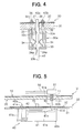
- FIG. 4 is a cross-sectional view of a connector of the indicating instrument illustrated in FIG. 3;
- FIG. 5 is a fragmentary cross-sectional side view illustrating a main portion of an indicating instrument according to a third embodiment of the invention.
- the indicating instrument according to a first embodiment of the invention is described with reference to FIGS. 1 and 2.
- the indicating instrument according to the first embodiment is installed into the passenger compartment of a car.
- the indicating instrument is generally comprised of a plurality of dial plate units U of substantially the same similar structure.
- a dial plate unit U is comprised of a dial plate 10 , a light conducting plate 20 , a printed circuit board 30 , a drive unit 40 , a luminous pointer 50 and light emitting diode 60 .
- the light conducting plate 20 receives light emitted from a light tube (not shown) disposed at a side edge thereof and conducts the light to the dial plate 10 to let the light penetrate dial plate 10 .
- the printed circuit board 30 has a printed circuit 32 of thin copper or aluminum films printed on a hard insulation board 31 .
- the printed circuit board 30 is disposed on the front surface of a drive control section 40 a of the drive unit 40 behind the light conducting plate 20 .
- the printed circuit board 30 may be a flexible circuit board that has an insulation board made of polyester or polyimide solid.
- the drive control section 40 a is comprised of a resinous casing 41 , which includes a case member 41 a , a terminal box 41 b and a common outer wall.
- the terminal box 41 b is fixed to an outer wall of the case member 41 a .
- the driving unit 40 also includes a rotary shaft 40 b .
- the case member 41 a has a ceiling 41 c and accommodates a step motor and a speed reduction gear train under the ceiling 41 c .
- the common outer wall extends upward from the ceiling 41 c and forms an enclosure wall 41 d.
- the step motor has a plurality of beam-like lead wires 42 .
- Each lead wire 42 extends from the inside of the case member 41 a into the terminal box 41 b along the ceiling 41 c inside the enclosure wall 41 d .
- Each lead wire 42 has a U-shaped portion that is accommodated in the terminal box 41 b and a terminal 42 a at the end of the portion thereof.
- Each lead wire 42 also extends radially outward from the case member and upward from the terminal box 41 b through the circuit board 30 .
- the terminal 42 a is soldered to a portion 41 e around a land hall of a printed circuit 32 of the circuit board 30 that is located remote from the rotary shaft 40 b .
- the ceiling 41 d of the casing 41 is fixed to the back of the circuit board 30 .
- the beam-like lead wires 42 may be disposed in close contact with the back of the circuit board 30 so that the heat generated while the light emitting diode 60 is powered can be dissipated through the lead wires 42 .
- the rotary shaft 40 b extends from ceiling 41 c of the casing 41 through a through hole 21 of the light conducting plate 20 and a through hole 11 of the dial plate 10 .
- the rotary shaft 40 b is connected to an output side of the speed reduction gear train disposed in the case member 41 a .
- the through hole 11 is formed at the center of dial plate 10 , or the center of an arc-shaped scale pattern.
- the luminous pointer 50 has a base portion 51 , which has a boss portion 51 a carried by the end of the rotary shaft 40 b .
- the luminous pointer 50 becomes luminous when it receives light of the light emitting diode 60 at the back of the base portion 51 through the through holes 21 and 11 .
- the light emitting diode 60 is a surface mounting type diode and fixed to a printed circuit 32 of the front surface of the circuit board 30 around the rotary shaft 40 b so that it can face the back of the base portion 51 through the through holes 21 and 11 .
- the light emitting diode 60 is powered from a DC electric source via the circuit board 30 to emit light and project the light through the through holes 21 and 11 to the base portion 51 of the pointer 50 .
- the light emitting diode 60 that is soldered to another portion of the circuit board 30 is about 10 mm distant from the terminal 42 a of the lead wire 42 that is soldered to a portion of the circuit board 30 . Therefore, heat of the soldering the terminal 42 a and the circuit board 30 does not damage the light emitting diode 60 .
- the light emitting diode 60 and other electric parts except the lead wires 42 a are soldered by a reflow or a flow soldering process to corresponding portions of the circuits 32 of the circuit board 30 . Even if the heat of such soldering is high and heat stresses are applied to the light emitting diode that is soldered to the circuit board 30 near the rotary shaft 40 b, the light emitting diode 60 is not damaged because such heat and stress are the first heat to be applied to the diode 60 .
- the casing 41 is fixed to the back of the circuit board 30 at the enclosure wall 41 d, and the terminal 42 a of the lead wires 42 are respectively inserted into land holes of the circuit board 30 . Thereafter, the terminals 42 a are respectively soldered to the corresponding portions 41 e of the printed circuit 32 . Because the light emitting diode 60 is about 10 mm distant from the terminals 42 a , the diode 60 is insulated from the soldering heat and the heat shocks. Since the casing 41 is fixed to the circuit board 30 after the high temperature due to the reflow or flow process has lowered, the resinous speed reduction gear train, which may not be heat resistant, can be protected from such high temperature. The resinous speed reduction gear train is also disposed remote from the terminal 42 a or soldered portion 41 e of the circuit board 30 . Therefore, the gear train is not damaged by the heat caused while the lead wires 42 are soldered to the circuit board 30 .
- the drive unit that includes the step motor can be substituted by a well-known cross-coil type drive unit.
- FIGS. 3 and 4 An indicating instrument according to a second embodiment of the invention is described with FIGS. 3 and 4.
- the same reference numeral in the following drawings corresponds to the same part or portion as the first embodiment.
- Each connector 30 a As many connectors 30 a as the lead wires 42 of circuit board are fixed to the back of the circuit board 30 and disposed inside the terminal box 40 b to respectively correspond to the lead wires 42 .
- Each connector 30 a has a cylindrical casing 33 , which has a ceiling 33 a fixed to the back of the circuit board 30 so as to receive corresponding one of the lead wires 42 and a pair of contact members 34 generally extending in parallel with the lead wire 42 .
- Each contact member 34 has an L-shaped contact edge 34 a that elastically presses against a middle portion of the outer periphery of the corresponding lead wire 42 .
- Each contact member 34 has an upper end 34 b that is inserted into one of land holes 35 of the circuit board 30 .
- Each land hole 35 is formed from a through hole of the insulation board 31 and a hole of the printed circuit 32 . The upper ends 34 b are soldered to the land holes 35 .
- Each terminal 42 a of the step motor is inserted into one of casings 33 through a through hole 33 b of the bottom thereof, between the pair of contact edges 34 a and through a through hole 33 c of the ceiling 33 a and is extended outward from a through hole 37 of the circuit board 30 . No portion of the printed circuit 32 exists around the through hole 37 .
- each connector 30 a is fixed to the back of the circuit board 30 at the ceiling 33 a , and the upper end 34 b of each contact member 34 is inserted into one of the land holes 35 . Thereafter, the terminal members 30 a of the connectors 30 a , the light emitting diode 60 and other electric parts are respectively soldered to the printed circuit 32 of the circuit board 30 by the reflow or flow soldering process. The upper ends 34 a of the pairs of contact members 34 are respectively soldered to circuit portions 36 of the corresponding land holes 35 , as shown in FIG. 4 .
- the light emitting diode 60 is not damaged because such heat and stress are the first heat to be applied to the diode 60 and not applied thereto any more.
- the casing 41 is fixed to the back of the circuit board 30 at the enclosure wall 41 d , and the connectors 30 a are accommodated in the terminal box 41 b .
- each terminal 42 a is inserted into the through holes 33 a , between the pair of contact members 34 a , the through hole 33 c of the ceiling and the through hole 37 of the circuit board 30 . Because no portion of the printed circuit 32 exists around the through hole 37 , the through holes 37 are not blocked by solder chips. Thus, the lead wires 42 are connected via the connectors 30 a to the circuit board 30 without soldering.
- the light emitting diode 60 can be used for illuminating the dial plate 10 instead of the light tube.
- a light intercepting portion is formed at the inner periphery of the through hole 21 of the light conducting plate 20 .
- a plurality of surface mounting-type light emitting diodes 70 is substituted for the light tube of the indicating instrument according to the first embodiment.
- the plurality of dial-plate illumination light emitting diodes 70 is mounted on the circuit 32 to correspond to the dial plate 10 .
- Each light emitting diode 70 emits light to the dial plate 10 through the light conducting plate 20 , so that uniform light as a whole can penetrate the dial plate 10 .
- the plurality of light emitting diodes 70 are disposed at a distance of about 10 mm from the soldered portion 41 e of the terminals 42 a around the rotary shaft 40 b and the light emitting diode 60 for illuminating the pointer 50 .
- the light emitting diodes 60 and 70 and other electric parts except the lead wires 42 a are soldered by a reflow or a flow soldering process to corresponding portions of the circuits 32 of the circuit board 30 . Even if the heat of such soldering is high and heat stresses are applied to the light emitting diodes 60 and 70 , the light emitting diodes 60 and 70 are not damaged because such heat and stress are the first heat to be applied to the diodes 60 and 70 .
- the casing 41 is fixed to the back of the circuit board 30 , and the terminal 42 a of the lead wires 42 are respectively inserted into land holes of the circuit board 30 . Thereafter, the terminals 42 a are respectively soldered to the corresponding portions 41 e of the printed circuit 32 . Because the light emitting diodes 60 and 70 are 10 mm or longer distant from the terminals 42 a , the diodes 60 and 70 are insulated from the soldering heat and the heat shocks.
- the light conducting plate 20 can be omitted.
- the luminous pointer 50 can be disposed behind the dial plate 10 .
Abstract
An indicating instrument includes a transparent dial plate, a printed circuit board disposed behind the dial plate, a drive unit disposed behind the printed circuit board having a plurality of lead wires soldered to the printed circuit board, a light conductive luminous pointer and a light emitting diode disposed on the printed circuit board near a rotary shaft so that the pointer can receive light emitted from the light emitting diode. Each end of the plurality of lead wires is disposed on the printed circuit board at a distance from the light emitting diode sufficient to insulate the light emitting diode from heat of soldering the plurality of lead wires to the circuit board.
Description
The present application is based on and claims priority from Japanese Patent Application 2000-97906 filed Mar. 30, 2000, the contents of which are incorporated herein by reference.
1. Field of the Invention
The present invention relates to an indicating instrument for various devices, and particularly, a vehicular indicating instrument having a luminous pointer.
2. Description of the Related Art
In a vehicular indicating instrument having a luminous pointer, a main portion of a drive unit is disposed behind a dial plate, and a rotary shaft extends outward from a through hole of the dial plate to carry a pointer at the end thereof. A pointer-illumination light emitting diode is disposed near the rotary shaft and the through hole behind the dial plate. A dial-plate-illumination light emitting diode may be also disposed near the rotary shaft behind the dial plate. Generally, such light emitting diodes are not sufficiently resistant to heat of soldering and a heat shock, if repeated.
If a step motor, which usually employs a resinous speed reduction gear train, is installed in the drive unit, it should be taken into account that such a step motor may not be resistant to the heat of soldering or heat shocks very much.
A main object of the invention is to provide an improved and reliable indicating instrument that includes a light emitting diode and other heat-sensitive parts.
According to a main feature of the invention in an indicating instrument that includes a transparent dial plate, a printed circuit board disposed behind the dial plate, a drive unit and a light conductive luminous pointer and a light emitting diode, a plurality of lead wires extended from the drive unit is respectively soldered to such distant portions on the printed circuit board from the diode that can insulate the diode from soldering heat.
Although the heat of soldering the light emitting diode to the circuit board is high and heat stresses are applied to the light emitting diode, the light emitting diode is not damaged because such heat and stress are the first heat to be applied to the diode and not applied thereto any more.
Other objects, features and characteristics of the present invention as well as the functions of related parts of the present invention will become clear from a study of the following detailed description, the appended claims and the drawings. In the drawings:
FIG. 1 is a fragmentary cross-sectional side view illustrating a main portion of an indicating instrument according to a first embodiment of the invention;
FIG. 2 is a perspective view of the indicating instrument according to the first embodiment;
FIG. 3 is a fragmentary cross-sectional side view illustrating a main portion of an indicating instrument according to a second embodiment of the invention;
FIG. 4 is a cross-sectional view of a connector of the indicating instrument illustrated in FIG. 3; and
FIG. 5 is a fragmentary cross-sectional side view illustrating a main portion of an indicating instrument according to a third embodiment of the invention;
An indicating instrument according to a first embodiment of the invention is described with reference to FIGS. 1 and 2. The indicating instrument according to the first embodiment is installed into the passenger compartment of a car. The indicating instrument is generally comprised of a plurality of dial plate units U of substantially the same similar structure. A dial plate unit U is comprised of a dial plate 10, a light conducting plate 20, a printed circuit board 30, a drive unit 40, a luminous pointer 50 and light emitting diode 60.
The light conducting plate 20 receives light emitted from a light tube (not shown) disposed at a side edge thereof and conducts the light to the dial plate 10 to let the light penetrate dial plate 10.
The printed circuit board 30 has a printed circuit 32 of thin copper or aluminum films printed on a hard insulation board 31. The printed circuit board 30 is disposed on the front surface of a drive control section 40 a of the drive unit 40 behind the light conducting plate 20. The printed circuit board 30 may be a flexible circuit board that has an insulation board made of polyester or polyimide solid.
The drive control section 40 a is comprised of a resinous casing 41, which includes a case member 41 a, a terminal box 41 b and a common outer wall. The terminal box 41 b is fixed to an outer wall of the case member 41 a. In addition to the drive control section 40 a, the driving unit 40 also includes a rotary shaft 40 b. The case member 41 a has a ceiling 41 c and accommodates a step motor and a speed reduction gear train under the ceiling 41 c. The common outer wall extends upward from the ceiling 41 c and forms an enclosure wall 41 d.
The step motor has a plurality of beam-like lead wires 42. Each lead wire 42 extends from the inside of the case member 41 a into the terminal box 41 b along the ceiling 41 c inside the enclosure wall 41 d. Each lead wire 42 has a U-shaped portion that is accommodated in the terminal box 41 b and a terminal 42 a at the end of the portion thereof. Each lead wire 42 also extends radially outward from the case member and upward from the terminal box 41 b through the circuit board 30. The terminal 42 a is soldered to a portion 41 e around a land hall of a printed circuit 32 of the circuit board 30 that is located remote from the rotary shaft 40 b. The ceiling 41 d of the casing 41 is fixed to the back of the circuit board 30.
The beam-like lead wires 42 may be disposed in close contact with the back of the circuit board 30 so that the heat generated while the light emitting diode 60 is powered can be dissipated through the lead wires 42.
The rotary shaft 40 b extends from ceiling 41 c of the casing 41 through a through hole 21 of the light conducting plate 20 and a through hole 11 of the dial plate 10. The rotary shaft 40 b is connected to an output side of the speed reduction gear train disposed in the case member 41 a. The through hole 11 is formed at the center of dial plate 10, or the center of an arc-shaped scale pattern.
The luminous pointer 50 has a base portion 51, which has a boss portion 51 a carried by the end of the rotary shaft 40 b. The luminous pointer 50 becomes luminous when it receives light of the light emitting diode 60 at the back of the base portion 51 through the through holes 21 and 11.
The light emitting diode 60 is a surface mounting type diode and fixed to a printed circuit 32 of the front surface of the circuit board 30 around the rotary shaft 40 b so that it can face the back of the base portion 51 through the through holes 21 and 11. The light emitting diode 60 is powered from a DC electric source via the circuit board 30 to emit light and project the light through the through holes 21 and 11 to the base portion 51 of the pointer 50. The light emitting diode 60 that is soldered to another portion of the circuit board 30 is about 10 mm distant from the terminal 42 a of the lead wire 42 that is soldered to a portion of the circuit board 30. Therefore, heat of the soldering the terminal 42 a and the circuit board 30 does not damage the light emitting diode 60.
In soldering, the light emitting diode 60 and other electric parts except the lead wires 42 a are soldered by a reflow or a flow soldering process to corresponding portions of the circuits 32 of the circuit board 30. Even if the heat of such soldering is high and heat stresses are applied to the light emitting diode that is soldered to the circuit board 30 near the rotary shaft 40 b, the light emitting diode 60 is not damaged because such heat and stress are the first heat to be applied to the diode 60.
After the soldering heat has dissipated, the casing 41 is fixed to the back of the circuit board 30 at the enclosure wall 41 d, and the terminal 42 a of the lead wires 42 are respectively inserted into land holes of the circuit board 30. Thereafter, the terminals 42 a are respectively soldered to the corresponding portions 41 e of the printed circuit 32. Because the light emitting diode 60 is about 10 mm distant from the terminals 42 a, the diode 60 is insulated from the soldering heat and the heat shocks. Since the casing 41 is fixed to the circuit board 30 after the high temperature due to the reflow or flow process has lowered, the resinous speed reduction gear train, which may not be heat resistant, can be protected from such high temperature. The resinous speed reduction gear train is also disposed remote from the terminal 42 a or soldered portion 41 e of the circuit board 30. Therefore, the gear train is not damaged by the heat caused while the lead wires 42 are soldered to the circuit board 30.
As a variation, the drive unit that includes the step motor can be substituted by a well-known cross-coil type drive unit.
An indicating instrument according to a second embodiment of the invention is described with FIGS. 3 and 4. In the meantime, the same reference numeral in the following drawings corresponds to the same part or portion as the first embodiment.
As many connectors 30 a as the lead wires 42 of circuit board are fixed to the back of the circuit board 30 and disposed inside the terminal box 40 b to respectively correspond to the lead wires 42. Each connector 30 a has a cylindrical casing 33, which has a ceiling 33 a fixed to the back of the circuit board 30 so as to receive corresponding one of the lead wires 42 and a pair of contact members 34 generally extending in parallel with the lead wire 42. Each contact member 34 has an L-shaped contact edge 34 a that elastically presses against a middle portion of the outer periphery of the corresponding lead wire 42. Each contact member 34 has an upper end 34 b that is inserted into one of land holes 35 of the circuit board 30. Each land hole 35 is formed from a through hole of the insulation board 31 and a hole of the printed circuit 32. The upper ends 34 b are soldered to the land holes 35.
Each terminal 42 a of the step motor is inserted into one of casings 33 through a through hole 33 b of the bottom thereof, between the pair of contact edges 34 a and through a through hole 33 c of the ceiling 33 a and is extended outward from a through hole 37 of the circuit board 30. No portion of the printed circuit 32 exists around the through hole 37.
In assembling, each connector 30 a is fixed to the back of the circuit board 30 at the ceiling 33 a, and the upper end 34 b of each contact member 34 is inserted into one of the land holes 35. Thereafter, the terminal members 30 a of the connectors 30 a, the light emitting diode 60 and other electric parts are respectively soldered to the printed circuit 32 of the circuit board 30 by the reflow or flow soldering process. The upper ends 34 a of the pairs of contact members 34 are respectively soldered to circuit portions 36 of the corresponding land holes 35, as shown in FIG. 4. Even if the heat of such soldering is high and heat stresses are applied to the light emitting diode 60, the light emitting diode 60 is not damaged because such heat and stress are the first heat to be applied to the diode 60 and not applied thereto any more.
After the soldering heat has dissipated, the casing 41 is fixed to the back of the circuit board 30 at the enclosure wall 41 d, and the connectors 30 a are accommodated in the terminal box 41 b. At the same time, each terminal 42 a is inserted into the through holes 33 a, between the pair of contact members 34 a, the through hole 33 c of the ceiling and the through hole 37 of the circuit board 30. Because no portion of the printed circuit 32 exists around the through hole 37, the through holes 37 are not blocked by solder chips. Thus, the lead wires 42 are connected via the connectors 30 a to the circuit board 30 without soldering.
As a variation of the above indicating instrument, the light emitting diode 60 can be used for illuminating the dial plate 10 instead of the light tube. For this purpose, a light intercepting portion is formed at the inner periphery of the through hole 21 of the light conducting plate 20.
An indicating instrument according to a third embodiment of the invention is described with reference to FIG. 5.
A plurality of surface mounting-type light emitting diodes 70 is substituted for the light tube of the indicating instrument according to the first embodiment. The plurality of dial-plate illumination light emitting diodes 70 is mounted on the circuit 32 to correspond to the dial plate 10. Each light emitting diode 70 emits light to the dial plate 10 through the light conducting plate 20, so that uniform light as a whole can penetrate the dial plate 10. The plurality of light emitting diodes 70 are disposed at a distance of about 10 mm from the soldered portion 41 e of the terminals 42 a around the rotary shaft 40 b and the light emitting diode 60 for illuminating the pointer 50.
In soldering, the light emitting diodes 60 and 70 and other electric parts except the lead wires 42 a are soldered by a reflow or a flow soldering process to corresponding portions of the circuits 32 of the circuit board 30. Even if the heat of such soldering is high and heat stresses are applied to the light emitting diodes 60 and 70, the light emitting diodes 60 and 70 are not damaged because such heat and stress are the first heat to be applied to the diodes 60 and 70.
After the soldering heat has dissipated, the casing 41 is fixed to the back of the circuit board 30, and the terminal 42 a of the lead wires 42 are respectively inserted into land holes of the circuit board 30. Thereafter, the terminals 42 a are respectively soldered to the corresponding portions 41 e of the printed circuit 32. Because the light emitting diodes 60 and 70 are 10 mm or longer distant from the terminals 42 a, the diodes 60 and 70 are insulated from the soldering heat and the heat shocks.
As a variation of the indicating instrument according to the third embodiment, the light conducting plate 20 can be omitted. In this variation, the luminous pointer 50 can be disposed behind the dial plate 10.
In the foregoing description of the present invention, the invention has been disclosed with reference to specific embodiments thereof. It will, however, be evident that various modifications and changes may be made to the specific embodiments of the present invention without departing from the scope of the invention as set forth in the appended claims. Accordingly, the description of the present invention is to be regarded in an illustrative, rather than a restrictive, sense.
Claims (11)
1. An indicating instrument comprising:
a transparent dial plate;
a printed circuit board disposed behind said dial plate;
a drive unit having a drive control section disposed behind said printed circuit board and a rotary shaft extending from said drive control section through said printed circuit board toward the center of said dial plate, said drive control section having a step motor and a plurality of lead wires soldered to said printed circuit board;
a light conductive luminous pointer having a base portion carried by said rotary shaft to rotate along the surface of said dial plate; and
a light emitting diode disposed on said printed circuit board near said rotary shaft so that said base portion of said pointer can receive light emitted from said diode, said light emitting diode being soldered to said printed circuit board; wherein
said printed circuit board has a first portion soldered to said light emitting diode and a second portion separately soldered to said plurality of lead wires disposed at a distance from said light emitting diode;
said drive control section comprises a case member for accommodating said step motor and a terminal box for accommodating said plurality of lead wires so that said rotary shaft and said plurality of lead wires respectively extend upward from said drive unit at opposite ends of said drive unit, whereby
each end of said plurality of lead wires is disposed on said printed circuit board at the distance from said light emitting diode to insulate said light emitting diode from heat of soldering said plurality of lead wires to said circuit board.
2. The indicating instrument as claimed in claim 1 , wherein
said distance is about 10 mm.
3. The indicating instrument as claimed in claim 1 , further comprising at least one additional light emitting diode, wherein
each of said light emitting diodes is disposed at the distance from said ends of said lead wires sufficient to insulate said light emitting diodes from heat of soldering said ends to said printed circuit board.
4. The indicating instrument as claimed in claim 1 , wherein
each said lead wire extends radially outward so that said end can be soldered to a portion that is located remote from said rotary shaft.
5. The indicating instrument as claimed in claim 1 , wherein each of said plurality of lead wires has a beam-like portion disposed in said case member and extended along said printed circuit board and a U-shaped portion disposed in said terminal box.
6. An indicating instrument comprising:
a dial plate having a through hole;
a printed circuit board disposed behind said dial plate;
a drive unit having a drive control section disposed behind said printed circuit board and a rotary shaft extending from said drive control section through said printed circuit board toward said through hole of said dial plate, said drive control section having a step motor and a plurality of lead wires soldered to said printed circuit board;
a light conductive luminous pointer having a base portion carried by an end of said rotary shaft via said through hole to rotate along the surface of said dial plate; and
a light emitting diode disposed on said printed circuit board near said rotary shaft so that said base portion of said pointer can receive light emitted from said light emitting diode through said through hole, said light emitting diode being soldered to said printed circuit board; wherein
said printed circuit board has a first portion soldered to said light emitting diode and a second portion separately soldered to said plurality of lead wires disposed at a distance from said light emitting diode;
said drive control section comprises a case member for accommodating said step motor and a terminal box for accommodating said plurality of lead wires so that said rotary shaft and said plurality of lead wires respectively extent upward from said drive unit at opposite ends of said drive unit, whereby
each of said plurality of lead wires has an end soldered to portions of said printed circuit board at the distance from said light emitting diode sufficient to insulate said light emitting diode from heat of soldering said ends to said printed circuit board.
7. The indicating instrument as claimed in claim 6 , wherein
said distance is about 10 mm.
8. The indicating instrument as claimed in claim 6 , further comprising at least one additional light emitting diode, wherein
said dial plate comprises a transparent member; and
each end of said plurality of lead wires is soldered to a portion of said printed circuit board at the distance sufficient to insulate said light emitting diodes from heat of soldering said ends to said printed circuit board.
9. An indicating instrument comprising:
a dial plate having a through hole;
a printed circuit board disposed behind said dial plate, said printed circuit board having a plurality of connectors soldered to said printed circuit board;
a drive unit having a drive control section disposed behind said printed circuit board and a rotary shaft extending from said drive control section through said circuit board toward said through hole of said dial plate, said drive control section having a step motor with a plurality of lead wires connected to said plurality of connectors and a resinous gear train connected between said step motor and said rotary shaft;
a light conductive luminous pointer having a base portion carried by an end of said rotary shaft to rotate along the surface of said dial plate; and
a light emitting diode disposed on said printed circuit board near said rotary shaft so that said base portion of said pointer can receive light emitted from said light emitting diode through said through hole, said light emitting diode being soldered to said printed circuit board, wherein
said printed circuit board has a first portion soldered to said light emitting diode and a second portion separately soldered to said plurality of lead wires disposed at a distance from said light emitting diode;
said drive control section comprises a case member for accommodating said step motor and a terminal box for accommodating said plurality of lead wires so that said rotary shaft and said plurality of lead wires respectively extend upward from said drive unit at opposite ends of said drive unit, whereby each end of said plurality of lead wire is disposed on said printed circuit board at the distance from said light emitting diode to insulate said diode from heat of soldering said plurality of lead wires to said circuit board.
10. The indicating instrument as claimed in claim 9 , further comprising at least one additional light emitting diode.
11. The indicating instrument as claimed in claim 10 , wherein
each of said light emitting diodes is a surface-mounting type diode, and
said printed circuit board comprises a first portion to which each of said light emitting diodes is soldered and a second portion to which said plurality of lead wires is soldered after said light emitting diodes is soldered.
Applications Claiming Priority (2)
| Application Number | Priority Date | Filing Date | Title |
|---|---|---|---|
| JP2000-97906 | 2000-03-30 | ||
| JP2000097906A JP4224924B2 (en) | 2000-03-30 | 2000-03-30 | Manufacturing method of indicating instrument |
Publications (2)
| Publication Number | Publication Date |
|---|---|
| US20010025596A1 US20010025596A1 (en) | 2001-10-04 |
| US6520109B2 true US6520109B2 (en) | 2003-02-18 |
Family
ID=18612467
Family Applications (1)
| Application Number | Title | Priority Date | Filing Date |
|---|---|---|---|
| US09/816,143 Expired - Lifetime US6520109B2 (en) | 2000-03-30 | 2001-03-26 | Heat insulation arrangement of indicating instrument |
Country Status (5)
| Country | Link |
|---|---|
| US (1) | US6520109B2 (en) |
| JP (1) | JP4224924B2 (en) |
| KR (1) | KR100388427B1 (en) |
| DE (1) | DE10113793A1 (en) |
| FR (1) | FR2807161B1 (en) |
Cited By (4)
| Publication number | Priority date | Publication date | Assignee | Title |
|---|---|---|---|---|
| US6714126B2 (en) * | 2001-03-30 | 2004-03-30 | Denso Corporation | Vehicle indicator unit having wowing and graduation lighting function |
| US20070189025A1 (en) * | 2003-08-29 | 2007-08-16 | Sonceboz Sa | Universal actuator particularly for dashboards |
| US7357095B1 (en) | 2004-04-05 | 2008-04-15 | Yazaki North America, Inc. | Transparent edge-lighted instrument cluster |
| US20110114009A1 (en) * | 2008-07-23 | 2011-05-19 | Yazaki Corporation | Pointer illumination structure |
Families Citing this family (5)
| Publication number | Priority date | Publication date | Assignee | Title |
|---|---|---|---|---|
| JP4414706B2 (en) * | 2002-09-20 | 2010-02-10 | 矢崎総業株式会社 | Dial module and method for manufacturing dial module |
| US6854853B2 (en) * | 2003-03-17 | 2005-02-15 | Visteon Global Technologies, Inc. | Method for wave soldering of surface mounted light emitting diodes |
| JP4583889B2 (en) * | 2004-11-12 | 2010-11-17 | 矢崎総業株式会社 | Instrument device |
| JP4719016B2 (en) * | 2006-01-27 | 2011-07-06 | 矢崎総業株式会社 | Pointer-type display device and method for manufacturing the pointer-type display device |
| EP2409384B1 (en) * | 2009-03-20 | 2013-07-17 | Kaltenbach & Voigt GmbH | Electric motor arrangement for a medical, especially dental, tool holder |
Citations (13)
| Publication number | Priority date | Publication date | Assignee | Title |
|---|---|---|---|---|
| USRE31073E (en) * | 1973-10-06 | 1982-11-02 | Kieninger & Obergfell Fabrik Fur Technische Laufwerke Und Apparate | Electromechanical clock |
| US4785434A (en) * | 1986-11-19 | 1988-11-15 | Casio Computer Co., Ltd. | Slip structure of a timepiece |
| US5142453A (en) * | 1989-10-26 | 1992-08-25 | Yazaki Corporation | Illuminant pointer needle assembly for vehicular instrument |
| US5143434A (en) * | 1990-03-30 | 1992-09-01 | Yazaki Corporation | Meter for automobiles |
| US5291851A (en) * | 1990-06-29 | 1994-03-08 | Yazaki Corporation | Gauge for automobile |
| US5531181A (en) * | 1994-03-28 | 1996-07-02 | Delco Electronics Corporation | Apparatus for illuminating instrument cluster pointers |
| US5546888A (en) * | 1994-09-09 | 1996-08-20 | Delco Electronics Corporation | Surface mounted gauge with illuminated pointer |
| US5612855A (en) * | 1994-06-14 | 1997-03-18 | Rudolf Schadow Gmbh | Adapter for mounting on a circuit board |
| US5690049A (en) * | 1996-02-05 | 1997-11-25 | Ford Motor Company | Compact gauge assembly |
| US5839810A (en) * | 1994-12-20 | 1998-11-24 | Robert Bosch Gmbh | Display gauge |
| US5857767A (en) * | 1996-09-23 | 1999-01-12 | Relume Corporation | Thermal management system for L.E.D. arrays |
| US5953213A (en) * | 1996-08-09 | 1999-09-14 | Robert Bosch Gmbh | Multichip module |
| US6335548B1 (en) * | 1999-03-15 | 2002-01-01 | Gentex Corporation | Semiconductor radiation emitter package |
-
2000
- 2000-03-30 JP JP2000097906A patent/JP4224924B2/en not_active Expired - Fee Related
-
2001
- 2001-03-21 DE DE10113793A patent/DE10113793A1/en not_active Ceased
- 2001-03-23 KR KR10-2001-0015132A patent/KR100388427B1/en not_active IP Right Cessation
- 2001-03-26 FR FR0104037A patent/FR2807161B1/en not_active Expired - Lifetime
- 2001-03-26 US US09/816,143 patent/US6520109B2/en not_active Expired - Lifetime
Patent Citations (13)
| Publication number | Priority date | Publication date | Assignee | Title |
|---|---|---|---|---|
| USRE31073E (en) * | 1973-10-06 | 1982-11-02 | Kieninger & Obergfell Fabrik Fur Technische Laufwerke Und Apparate | Electromechanical clock |
| US4785434A (en) * | 1986-11-19 | 1988-11-15 | Casio Computer Co., Ltd. | Slip structure of a timepiece |
| US5142453A (en) * | 1989-10-26 | 1992-08-25 | Yazaki Corporation | Illuminant pointer needle assembly for vehicular instrument |
| US5143434A (en) * | 1990-03-30 | 1992-09-01 | Yazaki Corporation | Meter for automobiles |
| US5291851A (en) * | 1990-06-29 | 1994-03-08 | Yazaki Corporation | Gauge for automobile |
| US5531181A (en) * | 1994-03-28 | 1996-07-02 | Delco Electronics Corporation | Apparatus for illuminating instrument cluster pointers |
| US5612855A (en) * | 1994-06-14 | 1997-03-18 | Rudolf Schadow Gmbh | Adapter for mounting on a circuit board |
| US5546888A (en) * | 1994-09-09 | 1996-08-20 | Delco Electronics Corporation | Surface mounted gauge with illuminated pointer |
| US5839810A (en) * | 1994-12-20 | 1998-11-24 | Robert Bosch Gmbh | Display gauge |
| US5690049A (en) * | 1996-02-05 | 1997-11-25 | Ford Motor Company | Compact gauge assembly |
| US5953213A (en) * | 1996-08-09 | 1999-09-14 | Robert Bosch Gmbh | Multichip module |
| US5857767A (en) * | 1996-09-23 | 1999-01-12 | Relume Corporation | Thermal management system for L.E.D. arrays |
| US6335548B1 (en) * | 1999-03-15 | 2002-01-01 | Gentex Corporation | Semiconductor radiation emitter package |
Cited By (6)
| Publication number | Priority date | Publication date | Assignee | Title |
|---|---|---|---|---|
| US6714126B2 (en) * | 2001-03-30 | 2004-03-30 | Denso Corporation | Vehicle indicator unit having wowing and graduation lighting function |
| US20070189025A1 (en) * | 2003-08-29 | 2007-08-16 | Sonceboz Sa | Universal actuator particularly for dashboards |
| US7503278B2 (en) * | 2003-08-29 | 2009-03-17 | Sonceboz Sa | Universal actuator particularly for dashboards |
| US7357095B1 (en) | 2004-04-05 | 2008-04-15 | Yazaki North America, Inc. | Transparent edge-lighted instrument cluster |
| US20110114009A1 (en) * | 2008-07-23 | 2011-05-19 | Yazaki Corporation | Pointer illumination structure |
| US8365680B2 (en) * | 2008-07-23 | 2013-02-05 | Yazaki Corporation | Pointer illumination structure |
Also Published As
| Publication number | Publication date |
|---|---|
| FR2807161A1 (en) | 2001-10-05 |
| US20010025596A1 (en) | 2001-10-04 |
| JP2001281011A (en) | 2001-10-10 |
| DE10113793A1 (en) | 2001-10-11 |
| KR20010094996A (en) | 2001-11-03 |
| KR100388427B1 (en) | 2003-06-25 |
| JP4224924B2 (en) | 2009-02-18 |
| FR2807161B1 (en) | 2006-06-23 |
Similar Documents
| Publication | Publication Date | Title |
|---|---|---|
| JP3059223B2 (en) | Controllers especially for automobiles | |
| US6598988B1 (en) | Display instrument, in particular in a motor vehicle | |
| US6520109B2 (en) | Heat insulation arrangement of indicating instrument | |
| EP0420650B1 (en) | Meter device | |
| US9705263B2 (en) | Plug connector assembly with light pipe and plural LEDs | |
| US6205031B1 (en) | Electronic control apparatus | |
| US6375477B2 (en) | Electronic device with connector and method of manufacturing the same | |
| JP2019145302A (en) | Light source unit for lighting appliance for vehicle and lighting appliance for vehicle | |
| US6702618B1 (en) | Modular jack having improved grounding plate | |
| JP4191437B2 (en) | Board-integrated brushless motor | |
| JP4840067B2 (en) | LED lamp device | |
| CN113895225B (en) | Meter device for vehicle | |
| US6744961B2 (en) | Optical module with metal casing accommodating electrically insulative holder for holding semiconductor package | |
| US6854853B2 (en) | Method for wave soldering of surface mounted light emitting diodes | |
| US20080219023A1 (en) | Printed circuit board for fitting with a punched grid | |
| US6407928B1 (en) | LED surface mount | |
| JP3343903B2 (en) | Instrument equipment | |
| JP2875300B2 (en) | Lamp device | |
| US6729775B2 (en) | Electro-optical module with a housing | |
| JPH11198740A (en) | Structure of assembling gauge on wiring board | |
| JP3104124B2 (en) | Capless light bulb device | |
| JPS5939733Y2 (en) | display device | |
| JP2003004489A (en) | Optical encoder | |
| JPH10335773A (en) | Mounting structure of electronic component | |
| JP2000136948A (en) | Structure for connecting electric instrument |
Legal Events
| Date | Code | Title | Description |
|---|---|---|---|
| AS | Assignment |
Owner name: DENSO CORPORATION, JAPAN Free format text: ASSIGNMENT OF ASSIGNORS INTEREST;ASSIGNOR:KOMURA, TAKASHI;REEL/FRAME:011924/0447 Effective date: 20010226 |
|
| STCF | Information on status: patent grant |
Free format text: PATENTED CASE |
|
| FPAY | Fee payment |
Year of fee payment: 4 |
|
| FPAY | Fee payment |
Year of fee payment: 8 |
|
| FPAY | Fee payment |
Year of fee payment: 12 |