US6522696B1 - Adaptive frequency correction in a wireless communications system, such as for GSM and IS54 - Google Patents
Adaptive frequency correction in a wireless communications system, such as for GSM and IS54 Download PDFInfo
- Publication number
- US6522696B1 US6522696B1 US08/832,719 US83271997A US6522696B1 US 6522696 B1 US6522696 B1 US 6522696B1 US 83271997 A US83271997 A US 83271997A US 6522696 B1 US6522696 B1 US 6522696B1
- Authority
- US
- United States
- Prior art keywords
- signal
- signals
- frequency offset
- bursts
- burst
- Prior art date
- Legal status (The legal status is an assumption and is not a legal conclusion. Google has not performed a legal analysis and makes no representation as to the accuracy of the status listed.)
- Expired - Fee Related
Links
Images


Classifications
-
- H—ELECTRICITY
- H04—ELECTRIC COMMUNICATION TECHNIQUE
- H04L—TRANSMISSION OF DIGITAL INFORMATION, e.g. TELEGRAPHIC COMMUNICATION
- H04L25/00—Baseband systems
- H04L25/02—Details ; arrangements for supplying electrical power along data transmission lines
- H04L25/03—Shaping networks in transmitter or receiver, e.g. adaptive shaping networks
- H04L25/03006—Arrangements for removing intersymbol interference
- H04L25/03178—Arrangements involving sequence estimation techniques
- H04L25/03248—Arrangements for operating in conjunction with other apparatus
- H04L25/03273—Arrangements for operating in conjunction with other apparatus with carrier recovery circuitry
-
- H—ELECTRICITY
- H04—ELECTRIC COMMUNICATION TECHNIQUE
- H04L—TRANSMISSION OF DIGITAL INFORMATION, e.g. TELEGRAPHIC COMMUNICATION
- H04L1/00—Arrangements for detecting or preventing errors in the information received
- H04L1/20—Arrangements for detecting or preventing errors in the information received using signal quality detector
-
- H—ELECTRICITY
- H04—ELECTRIC COMMUNICATION TECHNIQUE
- H04L—TRANSMISSION OF DIGITAL INFORMATION, e.g. TELEGRAPHIC COMMUNICATION
- H04L25/00—Baseband systems
- H04L25/02—Details ; arrangements for supplying electrical power along data transmission lines
- H04L25/03—Shaping networks in transmitter or receiver, e.g. adaptive shaping networks
- H04L25/03006—Arrangements for removing intersymbol interference
- H04L2025/0335—Arrangements for removing intersymbol interference characterised by the type of transmission
- H04L2025/03375—Passband transmission
- H04L2025/03401—PSK
- H04L2025/03407—Continuous phase
-
- H—ELECTRICITY
- H04—ELECTRIC COMMUNICATION TECHNIQUE
- H04L—TRANSMISSION OF DIGITAL INFORMATION, e.g. TELEGRAPHIC COMMUNICATION
- H04L27/00—Modulated-carrier systems
- H04L27/0014—Carrier regulation
- H04L2027/0024—Carrier regulation at the receiver end
- H04L2027/0026—Correction of carrier offset
- H04L2027/0028—Correction of carrier offset at passband only
-
- H—ELECTRICITY
- H04—ELECTRIC COMMUNICATION TECHNIQUE
- H04L—TRANSMISSION OF DIGITAL INFORMATION, e.g. TELEGRAPHIC COMMUNICATION
- H04L27/00—Modulated-carrier systems
- H04L27/0014—Carrier regulation
- H04L2027/0044—Control loops for carrier regulation
- H04L2027/0063—Elements of loops
- H04L2027/0065—Frequency error detectors
-
- H—ELECTRICITY
- H04—ELECTRIC COMMUNICATION TECHNIQUE
- H04L—TRANSMISSION OF DIGITAL INFORMATION, e.g. TELEGRAPHIC COMMUNICATION
- H04L27/00—Modulated-carrier systems
- H04L27/0014—Carrier regulation
- H04L2027/0083—Signalling arrangements
- H04L2027/0089—In-band signals
- H04L2027/0093—Intermittant signals
- H04L2027/0095—Intermittant signals in a preamble or similar structure
Definitions
- the present invention relates to communication systems, and more specifically to frequency error correction in a communication system.
- a transmitter sends information over a high frequency channel.
- a radio frequency upconverter converts a baseband signal to a high frequency signal prior to its transmission.
- a baseband signal can be upconverted in frequency by a multiplication process.
- This signal is mixed by the output signal of a local crystal oscillator that is tuned to a modulating frequency.
- the output signal of the mixer is the baseband signal shifted in frequency by an amount corresponding to the modulating frequency of the local crystal oscillator.
- a receiver receiving the transmitted signal first down converts the signal by shifting it back to a baseband frequency range.
- a local oscillator tuned to the modulating frequency is multiplied by the transmitted signal.
- a cellular communication system is one type of radio communication system mentioned above, in which radio telephones contain circuitry to permit transmission and reception of modulated signals.
- the radio telephones known as mobile stations, engage in a two-way communication with remotely located transceivers, known as base stations. These radio telephones also have a local crystal oscillator for down converting into baseband range, the signals that the base station transmits.
- the crystal oscillator frequency at the receiving station may not be exactly the same as the modulating frequency at the transmitter.
- This frequency offset between the transmitter and the receiver stations may cause communication errors.
- One of the possible reasons for this frequency offset is that the output frequency signal of the local oscillator may drift away from the intended modulating frequency over a period of time due to, for example, the ambient temperature variations at the receiver.
- Another possible reason for this frequency offset may be relative motion between a base and a mobile station. As it is well known, such relative motion between a transmitting and a receiving station, may result in a Doppler shift of the frequency of the signal being transmitted. This Doppler shift may therefore result in a phase/frequency error in the received signal, for example. Because of the ambient temperature variations at the receiving station and the Doppler shift described herein, for example, the integrity of the signal being transmitted may be corrupted at the receiving end of the communications system.
- a method for reducing frequency offset errors in a communications system comprises the steps of receiving a plurality of signal bursts; correcting the frequency error with the coarse frequency error estimate; decoding the received signal bursts by employing an equalizer, that generates a burst quality indication signal corresponding to the bit error rate in each received signal sample; generating a plurality of residual frequency offset signals corresponding to each signal burst; channel decoding said signal bursts generated by said equalizer so as to generate a channel quality signal repeating the bit error rate over a plurality of burst signals; accumulating residual frequency offset signals corresponding to bursts having acceptable burst quality indication signals and channel quality indication signals; acquiring a rotation frequency offset signal based on the accumulated residual frequency offset signals; and adjusting the phase of the received signal samples in accordance with the rotation frequency offset signal.
- FIG. 1 a is a block diagram illustrating one embodiment of a system employing adaptive frequency correction in accordance with the present invention.
- FIG. 1 b is a block diagram illustrating another embodiment of a system employing adaptive frequency correction in accordance with the present invention.
- FIG. 2 is a diagram illustrating a signal or transmission burst, such as for GSM.
- FIG. 3 illustrates a signal processor employed in a transmitter for transmitting signals, in accordance with one embodiment of the invention.
- FIG. 4 is a block diagram illustrating signal organization in accordance with one embodiment of the present invention.
- FIGS. 5 a through 5 c are plots of complex signals in the lnphase-Quadraturephase(I-Q) plane illustrating signal constellations with and without frequency offset errors.
- FIG. 6 is a block diagram of an equalizer in accordance with the embodiment of the present invention.
- FIG. 7 is a flowchart illustrating the operation of the embodiment of the present invention described with reference to FIGS. 1 a and 1 b.
- GSM global system for mobile communications
- FIG. 2 illustrates a signal burst also known as a transmission burst or a signal frame, such as may be employed in a wireless communication system, although the invention is not limited in scope to a signal burst having this particular form or format.
- the terms signal burst, transmission burst or signal frame may be used interchangeably.
- the signal or transmission burst illustrated in FIG. 2 has a predetermined number of digital signals or bits.
- each burst includes, in succession, a series of successive predetermined starting bits 27 , a predetermined number of information bits 29 , a series of predetermined training bits 31 , a second predetermined number of information bits 33 , and a series of successive predetermined ending bits 35 .
- GSM systems there are three starting and three ending bits, 57 bits in both portions of the signal burst comprising binary digital signals to be transmitted, and 26 training bits, referred to as the “midamble,” for a total of 148 bits per signal burst.
- the training bits are known at both the receiving and the transmitting end of the communications system.
- the starting and ending bits are likewise known and are typically “zeros.” It will be appreciated that other numbers and distribution of bits are possible depending on the implementation.
- the GSM telecommunication standard requires a form of signal modulation in the baseband known as Gaussian Minimum Phase Shift Keying (GMSK).
- GMSK Gaussian Minimum Phase Shift Keying
- the input bit or binary digital signal stream 20 is differentially encoded, e.g. baseband modulated, to produce a positive or negative 90° phase shift representing one or more binary digital signals in the signal burst being transmitted.
- This phase shift modulated baseband signal may then be applied to a radio frequency (RF) carrier for transmission.
- RF radio frequency
- the binary digital signals in the signal burst are processed by a process referred to as “derotation.” This process is applied to each signal sample in the signal burst.
- FIG. 3 illustrates a signal processor 10 employed in a transmitter for transmitting signals in accordance with GSM communications standard mentioned above.
- the signal processing scheme employed by signal processor 10 is well known and described in Mobile Radio Communications by Raymond Steele (Pentech Press Limited, 1992), and incorporated herein by reference.
- signal processor 10 includes a speech encoder 12 configured to encode speech signals for transmission in accordance with GSM standard.
- Speech encoder 12 delivers signal frames of 260 bits of data for each 20 ms of speech duration at a bit rate of 13 kbits/s.
- the output signal frames of speech encoder 12 are coupled to the input terminal of a cyclic coder 14 , which applies a cyclic code to each signal frame received from speech encoder 12 .
- the first 50 bits of each received frame are encoded by an error detecting block code.
- cyclic coder 14 generates three parity bits in response to the first 50 bits of the received frame. These parity bits are added to the received frame bringing the total number of bits in each frame to 263 bits.
- the output signal of cyclic coder 14 is coupled to an input terminal of a reordering and tailing bit circuit 16 .
- the first 182 bits of signal frames delivered by speech encoder 12 are reordered, such that bits with even indices are collected in the first part of a new data word, followed by the three parity bits generated by cyclic coder 14 , followed by bits with odd indices, followed by four zero tailing bits, followed by the remaining 78 encoded bits. This brings the length of each signal frame to 267 bits.
- the signal frame generated by reordering and tailing bits circuit 16 is then coupled to an input terminal of a convolutional coder 18 .
- the first 189 bits of signal frame received by convolutional coder may be encoded in accordance with known convolutional coding techniques as described in Mobile Radio communications , mentioned above.
- the 456 bits signal frame generated by convolutional coder 18 is then coupled to an input terminal of a partitioning circuit 20 .
- the partitioning circuit partitions the received signal frames into eight 57 bits long sub-blocks. These 57 bits long sub-blocks are then fed to a block-diagonal interleaving circuit 22 .
- FIG. 4 illustrates the format of signal bursts processed by block-diagonal interleaving circuit 22 .
- Circuit 22 processes the sub-block signals received from partitioning circuit 20 .
- each one of the frame numbers (n ⁇ 1), n and (n+1) comprises eight sub-blocks block B 0 through B 7 .
- each signal burst is made of sub-blocks of two consecutive frames received from partitioning circuit 20 .
- the output signals of block-diagonal interleaving circuit 22 is coupled to an input terminal of an interburst interleaving circuit 24 .
- Each signal burst is further interleaved by assigning the original received bits, c(n,k), into an interleaved sequence I(B, j) as stated below:
- Signals generated after interburst interleaving are then transmitted, via an antenna 26 , for reception by an intended receiver as will be explained in more detail hereinafter.
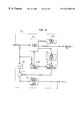
- FIG. 1 a is a block diagram of a receiver 28 that employs one embodiment of an adaptive frequency correction unit in accordance with the invention, although the invention is not limited in scope to this receiver or the frequency correction unit illustrated herein.
- Receiver 28 may be used to receive signals transmitted by a transmitter employing signal processor 10 of FIG. 3 .
- Receiver 28 includes an antenna 68 , which is configured to receive the transmitted signals.
- the output signals of antenna 68 is coupled to an input terminal of a radio frequency RF stage 30 , which comprises a down converter 60 , with an output terminal coupled to the input terminal of an analog to digital A/D converter 62 .
- the down converter includes a crystal oscillator that is approximately tuned to the modulating frequency of the transmitted signal.
- the output signal of the down converter is a baseband signal, which is fed into analog-to-digital converter 62 to produce baseband signal samples.
- This analog-to-digital (A/D) conversion may be performed, for example, by a baseband CODEC, which digitizes the baseband analog signal.
- An example of a down converter 60 and A/D converter 62 to perform such A/D conversion includes the W2020 GSM Transceiver and CSP1088 GSM Conversion Signal Processor, both available from Lucent Technologies Inc. or AT&T Corp., although the invention is not restricted in scope to the use of a baseband CODEC to perform the A/D conversion or to these particular devices.
- the invention is not limited in scope to an embodiment in which A/D conversion is performed so that binary signal processing may be employed. Likewise, the invention is not limited in scope to performing A/D conversion at this particular point in the signal path. For example, A/D conversion may be performed earlier in the signal path, such as before removal of the carrier frequency, or later in the signal path, depending on the particular embodiment.
- the output terminal of analog to digital converter 62 is coupled to an adaptive frequency correction AFC rotation sub-unit 32 .
- Another input terminal of AFC rotation sub-unit 32 is configured to receive a rotation frequency offset signal, AFC_F_rotor.
- This unit 32 rotates the phase of the incoming signals based on the rotation frequency offset signal, in order to reduce communication errors, as will be explained in more detail.
- this frequency offset signal is used to rotate the receiver signal to stabilize the rotating signal constellation.
- the corrected signals are then coupled to an input terminal of an equalizer 34 and an input terminal of a synchronizer 52 .
- Equalizer 34 is employed to decode the signals received by receiver 28 .
- One of the output terminals of equalizer 34 is coupled to an input terminal of a deinterleaver 36 .
- equalizer 34 Another output terminal of equalizer 34 provides a residual frequency offset signal, AFC_F_res, to an input terminal of automatic frequency correction unit 58 , as will be explained below.
- the third output terminal of equalizer 34 is also coupled to an input terminal of an automatic frequency correction unit 58 to provide an equalizer quality, or burst quality signal, Burst_Qual. This burst quality signal represents the effectiveness of signal estimation accomplished by equalizer 34 .
- Synchronizer 52 comprises a phase derotator 64 , and an offset estimator 66 .
- Synchronizer 52 is used to provide an initial frequency estimate in response to a set of known signals transmitted by the transmitter at predetermined intervals, as will be explained in more detail hereinafter.
- An input terminal of phase derotator 64 is configured to receive signals from adaptive frequency correction, AFC, rotation sub unit 32 .
- the output terminal of phase derotator 64 is coupled to offset estimator 66 , which provides an initial or coarse frequency offset signal to automatic frequency correction unit 58 .
- Deinterleaver 36 performs the reverse function employed by interburst interleaving circuit 24 of FIG. 3 .
- the output terminal of deinterleaver 36 is coupled to a block deinterleaver 38 , which performs the reverse function employed by block diagonal interleaving circuit 22 .
- the output signal of block deinterleaver 38 may appear substantially similar to signal bursts illustrated in FIG. 4 .
- One output terminal of block deinterleaver 38 is coupled to a comparator 56 .
- the other output terminal of block deinterleaver 38 is coupled to the input terminal of a departitioning circuit 40 , which performs the reverse function employed by departitioning circuit 20 of FIG. 3 .
- the output terminal of departitioning circuit is coupled to the input terminal of a channel decoder 42 , which performs the reverse function employed by convolutional coder 18 of FIG. 3 .
- channel decoder 42 comprises a Viterbi decoder. The operation of Viterbi decoder is described in more detail below.
- An output terminal of channel decoder 42 is coupled to a channel encoder 44 , which is configured to encode the signals received from the channel decoder.
- Channel encoder 44 comprises a convolutional coder 46 that performs substantially the same as convolutional coder 18 of FIG. 3 .
- the output terminal of convolutional coder 46 is coupled to the input terminal of a partitioning circuit 48 that performs substantially the same as partitioning circuit 20 .
- the output terminal of a partitioning circuit 48 is coupled to the input terminal of a block diagonal interleaving circuit 50 , which operates substantially the same as block diagonal interleaving circuit 22 of FIG. 3 .
- the output signal of block diagonal interleaving 50 is coupled to another input terminal of comparator 56 .
- the output signal of comparator 56 is coupled to an input terminal of adaptive frequency correction unit 58 . This output signal is referred to as sub-frame bit error quality indication signal or channel quality indication signal, RXQUAL.
- the output signal of channel decoder 42 is also coupled to the input terminal of an ordering and tailing circuit 70 which performs the reverse function of circuit 16 of FIG. 3, and provides a signal to an input terminal of a cyclic decoder 72 .
- the cyclic decoder performs the reverse function employed by cyclic coder 14 of FIG. 3 .
- the output signal of cyclic decoder 72 is coupled to an input terminal of a speech decoder 74 , which performs the reverse function employed by speech encoder 12 of FIG. 3 .
- Adaptive frequency correction unit 58 is responsible for acquiring and tracking the relative frequency or phase offset between signals shifted in response to automatic frequency correction rotation sub-unit 32 and signals transmitted by a transmitter employing signal processor 10 .
- the adaptive frequency correction unit then provides a feedback signal to adaptive frequency correction rotation subunit 32 .
- This feedback signal represents a rotation frequency offset signal, AFC_F_rotor, calculated by the adaptive frequency correction unit.
- adaptive frequency correction rotation sub-unit 32 rotates the phase of incoming signals in accordance with the rotation frequency offset signal AFC_F_rotor, so as to adjust their phase and substantially reduce communication errors.
- Adaptive frequency correction unit 58 employs an adaptive update and tracking algorithm, as will be explained in more detail below, to update and track the relative frequency offset between the signals transmitted and the signals received by receiver 28 .
- This relative frequency offset is measured based on the signals coupled to input terminals of adaptive frequency correction unit 58 .
- These signals may include: (1) an initial or coarse frequency offset estimate signal, which is the frequency or phase delay acquired by synchronizer 52 , for signals received by receiver 28 .
- This initial estimate is only a coarse estimate of frequency offset or phase delay between the signals transmitted and signals received by receiver 28 ; (2) an instantaneous residual frequency or phase offset signal, AFC_F_res, acquired by equalizer 34 , which provides a more accurate estimate of this frequency offset or phase delay; a burst accumulated cost signal, Burst_Qual, which represents the equalizer quality, as will be explained in more detail below; and the sub-frame bit error quality indication signal, also referred to as channel quality indication signal, RXQUAL, provided by comparator 56 .
- Equalizer 34 continuously provides the residual frequency offset signal, AFC_F_res, to automatic frequency correction unit 58 .
- This residual frequency offset signal, AFC_F_res may be used by adaptive frequency correction unit 58 if it is qualified as acceptable based on the burst accumulated cost signal, Burst_Qual, provided by equalizer 34 , and based on the sub-frame bit error quality indication signal, or channel quality indication signal, RXQUAL, provided by comparator 56 .
- Adaptive frequency correction unit 58 also measures a reference frequency offset, AFC_F_ref accumulating residual frequency offset signals, AFC_F_res derived from a predetermined number of acceptable burst signals, as indicated by quality indication signal, RXQUAL, to obtain an accumulated residual frequency offset signal AFC_F_acc, and dividing the AFC_F_acc signal over the number of residual frequency signals AFC_F_res accumulated.
- each signal burst at the output terminal of deinterleaver 36 comprises a partial sequence of data from one speech frame n, and a partial sequence of data from another speech frame n ⁇ 1.
- equalizer 34 decodes the incoming signals based on an estimate of these signals, there may be a certain number of bit errors in the output signal of deinterleaver 36 . After these signals have traveled through block deinterleaver 38 , departitioning unit 40 , and channel decoder 42 , these bit errors are substantially eliminated.
- Channel encoder 44 again reconstructs the signals following the same structure illustrated in FIG. 4 .
- the output signal of channel encoder 44 is substantially free of error. This output signal is compared with the output signal of deinterleaver 36 . It will, of course, be appreciated that when signal processor 10 of FIG. 3 lacks an interleaver 24 , the output signal of channel encoder 44 is compared with the output signal of equalizer 34 .
- the channel quality indication signal RXQUAL corresponds to the number of mismatches in the bits received from channel encoder 44 and deinterleaver 36 , or alternatively equalizer 34 .
- RXQUAL(n) signal is declared acceptable by automatic frequency correction unit 58 , if the bit error count over a speech frame is below a predetermined threshold.
- RXQUAL(n ⁇ 1) indicates a good frame detection
- RXQUAL(n) indicates a bad frame detection
- sub-blocks B n 0 , B n 1 B n 2 , B n 3 are possibly acceptable
- sub-blocks B n 4 , B n 5 B n 6 , B n 7 are in error.
- residual frequency error acquired over bursts 4 through 7 may be discarded by automatic frequency correction unit 58 , while residual frequency error signal acquired over bursts 0 through 3 may be used, provided that the remaining conditions mentioned above are met.
- This embodiment of the invention provides a more simple approach to measure the received burst quality for each speech frame.
- Synchronizer 52 provides a coarse frequency offset error or phase delay signal, AFC_F_synch, at predetermined intervals, which is an estimate of the frequency offset between the frequency of the local oscillator and that of the transmitted signals.
- AFC_F_synch a coarse frequency offset error or phase delay signal
- synchronizer 52 is substantially similar to a synchronizer described in the co-pending U.S. patent application Ser. No. 08/357,003, entitled” Oscillator Frequency Offset Error Estimator For a Wireless Communication System, Such As For Use With GSM,” (Mobin 25), by M.S. Mobin, filed Dec. 16, 1996, abandoned Jul. 3, 1996 and refiled on Jul. 3, 1996, Ser. No.
- Synchronizer 52 responds to a series of predetermined binary bits such as zero's, known as frequency correction bits “FCB's”. These FCB bits are transmitted by a transmitter at predetermined intervals.
- Phase derotator 64 applies a 90° phase shift to each differentially encoded symbol or signal sample in the signal burst transmitted via the wireless medium. For example, each signal sample is multiplied by ⁇ j ⁇ ⁇ ⁇ 2 ⁇ ⁇ k ,
- phase derotator 64 The output signal of phase derotator 64 is coupled to a phase offset error estimator 66 , which is used to determine the phase offset error as a result of a difference in frequency between the modulating frequency of the transmitted signal and the frequency of the crystal oscillator within downconverter 30 .
- frequency offset error estimator The operation of frequency offset error estimator according to one embodiment of the invention is described in reference to FIGS. 5 a through 5 c .
- signal processor 10 of FIG. 2 periodically sends a set of binary “zero” frequency correction bits, FCB's, that are used to calculate the frequency or phase offset error generated at the receiver.
- FIG. 5 a illustrates an idealized signal constellation in the I-Q plane of a frequency burst of “zero” signals that have been encoded in accordance with GSM GMSK specified modulation.
- each differentially encoded bit value produces a phase shift in the I-Q plane of 90°, as illustrated in FIG. 5 a . This corresponds to a counter-clockwise rotation in the I-Q plane for a stream of binary digital signal “zeros” being transmitted.
- FIG. 5 b illustrates the effect of the frequency offset error on the signal constellation in the I-Q plane of the same frequency burst of “zero” signals that have been encoded in accordance with GSM GMSK specified modulation.
- a first baseband signal denoted (I 1 , Q 1 ) in rectangular coordinates.
- An initial offset error, ⁇ 0 may be imparted to the incoming signals.
- the next signal which is also a zero, should have a counter-clockwise rotation of 90°.
- the resulting signal I 2 ,Q 2 is oriented at d ⁇ plus 90° with respect to I 1 , Q 1 .
- the resulting signal I 3 , Q 3 of the following zero is oriented at d ⁇ plus 90° with respect to I 2 , Q 2 and so forth, where d ⁇ is the additional phase offset due to frequency offset error, of one signal to the other.
- phase derotator 64 is used to derotate the phase of incoming baseband signals by ⁇ k ⁇ /2 radians, such that the incoming signals of “zeros” are all desirably shifted to a fixed point on the constellation, such as the “+1” location in the I-Q plane.
- FIG. 5 c illustrates the result of this derotation. Due to the frequency offset error, each incoming signal after derotation falls within d ⁇ of the previous signal.
- Equalizer 34 includes a Viterbi decoder 114 , used to receive and decode input signals from AFC rotation sub-unit 32 (FIG. 1 ).
- equalizer 34 may be implemented using a digital signal processor DSP1618 available from Lucent Technologies Inc., which includes an embedded error correction coprocessor (ECCP) for operating as Viterbi decoder 114 , described in the preliminary data sheet, dated February 1994, available from Lucent Technologies Inc. or AT&T Corp., herein incorporated by reference, although the scope of the invention is not limited in this respect.
- DSP1618 available from Lucent Technologies Inc.
- ECCP embedded error correction coprocessor
- Equalizer 34 also includes a channel estimator 116 used to measure an estimate of the characteristics of the communications channel through which the signals are being transmitted.
- the output terminal of the channel estimator 116 is coupled to Viterbi decoder 114 and to a signal reconstructor 118 .
- Viterbi decoder 114 produces two output signals, one of which provides a long version of decoded output signal to a decoded output register 129 .
- the other output signal of the Viterbi decoder provides a short decoded output signal to a short decoded output register 132 , also coupled to signal reconstructor 118 .
- the output terminal of the signal reconstructor is coupled to a multiplier 120 , which also receives an input signal from AFC rotation sub-unit 32 through a delay register 122 .
- Multiplier 120 performs a complex conjugate multiplication and provides an output signal fed into a residual frequency offset register 124 .
- the output signal provided by register 124 represents the phase difference between the input signal sample provided to the equalizer and an estimated signal sample derived from the equalizer.
- the output signal of residual frequency offset register 124 is in turn coupled to automatic frequency correction unit 58 .
- Viterbi decoder 114 in conjunction with channel estimator 116 is described in the aforementioned U.S. Pat. No. 5,465,275, patented Nov. 7, 1995 entitled “Efficient Utilization of Present State/Next State Registers,” filed Nov. 16, 1993, by D D. Blaker, M. Diamondstein, G. Ellard, M. Mobin, H. Sam and M. Thierbach (Blaker 3-2-3-3-4-10) and U.S. Pat. No. 5,592,514, entitled “Method Of Performing Signal Reconstruction At the Receiving End of a Communications System, Such As For GSM,” (Mobin 20) by M. S. Mobin filed Mar.
- Viterbi decoder 114 is a maximum likelihood decoder that provides forward error correction.
- the Viterbi decoder works back through a sequence of possible bit sequences at each symbol instant to determine which one bit sequence is most likely to have been transmitted.
- the possible transitions from a bit at one symbol instant, or state, to a bit at a subsequent, symbol instant or state is limited.
- Each possible transition from one state to a next state may be illustrated graphically and is referred as a branch in this context.
- a sequence of interconnected branches is referred to as a path in this context.
- Each state may transition only to a limited number of next states upon receipt of the next bit (or set of bits) in the bit stream.
- potential paths remain while other potential paths are eliminated during the decoding process. By eliminating those paths that are not permissible, computational efficiency may be achieved in determining the most likely paths to have been transmitted.
- Channel estimator 116 uses the training bits of an incoming burst as illustrated in FIG. 2, to calculate an estimate of the channel over which the transmission occurred.
- This channel estimate is the impulse response function of the communication channel through which the bursts are being transmitted from a transmitter station to a receiver station, such as receiver 28 .
- the received signal is distorted due to noise and inter symbol interference associated with transmission via the communications channel.
- an estimate of the channel is obtained.
- Each term in the impulse function is a complex quantity and is referred to in this context as a tap weight or channel tap.
- Each tap weight represents the effects of channel distortion on the transmitted signal.
- Viterbi decoder 114 receives the tap weights generated by channel estimator 116 . It then convolves these tap weights with all possible combinations of Viterbi states to obtain a reconstructed signal for each state.
- the Viterbi states represent all possible next states in the transmission. The convolution is achieved by convolving all 2 C possible states, representing the Viterbi states with the channel tap estimates, to obtain an estimate of the received signal for each candidate state that is employed in a process referred to in this context as branch metric processing.
- the Viterbi decoder typically processes a branch metric associated with each branch transition and employs this branch metric to determine the remaining paths as previously described.
- a branch metric is processed at each symbol instant for each possible transition from one individual state to the next individual state according to
- BM is the branch metric quantity
- I, Q are the components of each reconstructed signal sample
- I′ Q′ are the components of the received signal sample.
- the branch metric of both branches transitioning to a given next individual state are processed, then added to the accumulated cost of the respective originating individual state, resulting in two potential accumulated cost sums. A comparison is made of the two potential accumulated cost sums. The lesser of the two sums is selected as the next state accumulated cost as follows:
- UACE(n) is the updated accumulated cost estimate of Viterbi state n
- PSAC(n) is the present accumulated cost estimate of Viterbi state n
- BM(n) is the branch metric for Viterbi state n.
- the transition corresponding to the lesser sum is the more likely transition from the two possible originating individual states to the given next individual state.
- the originating individual state of the more likely transition is stored as the surviving origin of a branch to the given next individual state.
- the lesser sum is the accumulated cost of the next individual state and replaces the accumulated cost for that individual state. This process is repeated for each of the next individual states and repeated also for each symbol instant until all symbols in the bit stream of one signal burst are decoded.
- the updated Viterbi state cost for each transmission of a signal burst is an indication of the amount of bit error rate of the Viterbi decoder. This final updated state cost may be represented by the Burst_Qual signal described above.
- the Burst_Qual signal may be compared with a predetermined threshold. If the updated state cost is above this threshold, the number of errors corrected by the Viterbi decoder is considered to be an unacceptable rate. In response, the Viterbi decoder provides an unacceptable equalizer quality signal indication via equalizer quality line 130 (FIG. 1 ). If, on the other hand, the updated state cost is below the predetermined threshold, the number of corrected errors by the Viterbi decoder falls within an acceptable range. The Viterbi decoder provides an acceptable equalizer quality signal indication over equalizer quality line 130 . Therefore, for each received burst, the equalizer quality may be determined. Likewise, equalizer quality may also be determined by decoding a sequence of bits shorter than a transmitted signal burst or larger than a transmitted signal burst. The automatic frequency correction unit receives an indication of the equalizer quality over equalizer quality line 130 .
- signal reconstructor 118 The operation of signal reconstructor 118 is described in more detail in reference with FIG. 6 .
- the output signal of Viterbi decoder 114 is fed to a short decoded output register 132 .
- This register provides a decoded signal to signal reconstructor 118 .
- the signal reconstructor retrieves the estimated channel taps generated by channel estimator 116 . It then reencodes the decoded signal it received from the Viterbi decoder, by convolving the channel taps with the decoded signal. The result of this convolution is an estimated reconstructed signal.
- the output signal of signal reconstructor 118 is subjected at a multiplier 120 to a complex conjugate multiplication with the original received signal coming through the delay register 122 .
- the output signal of multiplier 120 is the residual frequency offset error signal AFC_F_res, which is stored in the residual frequency offset register 124 .
- the Doppler offset error due to the errors caused by Doppler shift may also be stored in register 124 .
- the Doppler phase offset error is derived according to the description in patent application Ser. No. 08/401,058, entitled “Method of Compensating For Doppler Error In a Wireless Communications System, Such As for GSM And IS54,” (Mobin 18) by M. S. Mobin, filed Mar. 8, 1995, and incorporated herein by reference, although this invention is not limited in scope to this implementation of Doppler error estimation, or Doppler error estimation in general.
- FIG. 1 b illustrates another embodiment of receiver 28 in accordance with the present invention.
- receiver 28 does not employ a channel reencoder 44 .
- an output signal of the Viterbi decoder in channel decoder 42 is directly coupled to an input terminal of automatic frequency correction unit 58 , via line 131 .
- This output signal of Viterbi decoder may be configured so as to represent the accumulated cost over four consecutive signal bursts received from departitioning unit 40 .
- the operation of Viterbi decoder 42 is substantially the same as the operation of Viterbi decoder 114 explained in FIG. 1 a .
- Viterbi decoder 114 measures the accumulated cost for one signal burst
- Viterbi decoder of channel decoder 42 measures the updated Viterbi state cost for four signal bursts although the invention is not limited in scope in that respect.
- sub-frame bit error, RXQUAL (n) comprises the updated state cost over four received signal bursts from one speech frame, and the final updated state cost over four received signal burst over the next speech frame.
- this updated state cost, RXQUAL signal is compared with a predetermined threshold. If the updated state cost is above this threshold, the number of errors made by the Viterbi decoder is considered to be above an acceptable rate. In response, the Viterbi decoder provides an unacceptable RXQUAL signal indication via RXQUAL quality line 131 . If, on the other hand, the updated state cost is below the predetermined threshold, the number of corrected errors by the Viterbi decoder falls within an acceptable range. The Viterbi decoder provides an acceptable RXQUAL quality signal indication over RXQUAL quality line 131 . Thus, Viterbi decoder of channel decoder 42 provides a signal that corresponds to a sub-frame bit error rate.
- FIG. 7 is a flowchart depicting a pseudo code sequence of the operation of the automatic frequency correction unit 58 employed in this particular embodiment of the present invention.
- the system at step 200 initializes the automatic frequency correction unit 58 .
- Frequency correction unit 58 operates in two modes: training or transient mode and tracking or steady state mode.
- training or transient mode When a receiving station is first turned on or when it is reset, the initialization step 200 begins, while the frequency correction unit 58 is in the training mode.
- automatic frequency correction unit 58 sends the latest frequency offset signal, AFC_F_synch, determined by synchronizer 52 to AFC rotation sub-unit 32 .
- automatic frequency correction rotation sub-unit 32 generates a rotation frequency offset signal AFC_F_rotor, substantially equal to frequency offset signal, AFC_F_synch.
- Rotation frequency offset signal AFC_F_rotor is used to rotate the incoming down-converted signals so as to adjust their phase.
- automatic frequency correction unit 58 sets the average residual frequency offset signal, AFC_F_ref to zero. It also sets a counter accumulation Count to zero.
- automatic frequency correction unit 58 initializes accumulated residual frequency offset signal to zero.
- automatic frequency correction unit 58 accumulates residual frequency offset signals, AFC_F_res, obtained from equalizer 34 over four bursts.
- automatic frequency correction unit 58 evaluates RXQUAL signal. If RXQUAL signal indication is acceptable, the accumulated frequency offset signal AFC_F_acc is accumulated with the value derived at step 206 . At the same time the counter accumulation Count signal is incremented by four.
- automatic frequency correction unit 58 continues residual frequency offset accumulation, as explained in steps 204 , 206 and 208 , until the counter accumulation Count signal has reached a predetermined threshold, such as 4*N 1 , where N 1 is a predetermined number.
- automatic frequency correction unit 58 calculates the average residual frequency offset signal, AFC_F_ref by dividing accumulated residual frequency signal, AFC_F_acc over 4*N 1 , and sets counter accumulation Count signal to zero.
- automatic frequency correction unit 58 enters its steady state. It sets the accumulated residual frequency offset signal, AFC_F_acc to zero.
- unit 58 determines an accumulated residual frequency offset signal by accumulating residual frequency offset signals, AFC_F_res, over four bursts, if the Burst_Qual signal derived from equalizer 34 is below a given threshold, and each residual frequency offset signal is smaller than the average residual frequency offset signals, AFC_F_ref.
- automatic frequency correction unit 58 accepts the accumulated residual frequency offset signal, derived at step 216 , if RXQUAL signal indication is acceptable. Unit 58 also increments the counter Count by four. Otherwise, unit 58 , discards the accumulated residual frequency offset signal, derived at step 216 . At step 220 , unit 58 repeats steps 216 and 218 , until, counter Count reaches a predetermined number 4*N 2 , where N 2 is a given number.
- rotation frequency offset signal AFC_F_rotor is updated by an average frequency signal AFC_F_acc, derived from steps 216 through 220 .
- unit 58 continues AFC tracking by returning to step 202 , if automatic frequency correction unit is enabled. Otherwise, Unit 58 goes to an idle state at step 226 .
- step 226 if AFC is enabled, it returns to step 202 . Otherwise, it resets AFC_F_acc count to zero and goes to step 228 .
- Steps 228 to 232 are referred to as a warm-start procedure.
- unit 58 emerges out of the idle state and enters a steady state cycle.
- unit 58 measures the accumulated residual frequency offset signals, by adding residual frequency offset signals obtained from equalizer 34 .
- unit 58 considers this accumulated residual frequency offset signal and increments the counter Count by 4.
- unit 58 continues steps 228 and 230 , as long as the number of received signal bursts is within a predetermined threshold. Otherwise, unit 58 goes to its idle state 226 . Thereafter, if automatic frequency correction is enabled, Unit 58 goes to step 202 again for reinitialization.
- the automatic frequency correction unit also measures the remaining frequency offset error imposed by a Doppler shift.
- the remaining offset frequency register 124 would include the frequency offset error due to both Doppler shift and crystal oscillation offset between the transmitter and the receiver.
- an automatic frequency correction unit provides a more accurate estimate of phase offset error than those provided by prior art systems. Furthermore, channel quality and equalizer quality estimation provide an effective criteria to evaluate the reception quality of the receiver, allowing for an effective phase offset correction.
Abstract
Description


Claims (19)
Priority Applications (1)
| Application Number | Priority Date | Filing Date | Title |
|---|---|---|---|
| US08/832,719 US6522696B1 (en) | 1997-04-11 | 1997-04-11 | Adaptive frequency correction in a wireless communications system, such as for GSM and IS54 |
Applications Claiming Priority (1)
| Application Number | Priority Date | Filing Date | Title |
|---|---|---|---|
| US08/832,719 US6522696B1 (en) | 1997-04-11 | 1997-04-11 | Adaptive frequency correction in a wireless communications system, such as for GSM and IS54 |
Publications (1)
| Publication Number | Publication Date |
|---|---|
| US6522696B1 true US6522696B1 (en) | 2003-02-18 |
Family
ID=25262440
Family Applications (1)
| Application Number | Title | Priority Date | Filing Date |
|---|---|---|---|
| US08/832,719 Expired - Fee Related US6522696B1 (en) | 1997-04-11 | 1997-04-11 | Adaptive frequency correction in a wireless communications system, such as for GSM and IS54 |
Country Status (1)
| Country | Link |
|---|---|
| US (1) | US6522696B1 (en) |
Cited By (28)
| Publication number | Priority date | Publication date | Assignee | Title |
|---|---|---|---|---|
| US20020015401A1 (en) * | 2000-08-03 | 2002-02-07 | Ravi Subramanian | Flexible TDMA system architecture |
| US20020075966A1 (en) * | 2000-10-31 | 2002-06-20 | Mikkola Hannu J. | Method and arrangement for providing optimal bit protection against transmission errors |
| US20020101943A1 (en) * | 2001-01-29 | 2002-08-01 | Tantivy Communications, Inc. | Method and apparatus for detecting rapid changes in signaling path environment |
| US20020106992A1 (en) * | 2000-10-27 | 2002-08-08 | Nokia Corporation | Synchroniser |
| US20030147456A1 (en) * | 2000-08-29 | 2003-08-07 | Takahiro Kumura | Frequency offset estimator |
| US20040105396A1 (en) * | 2002-11-08 | 2004-06-03 | Thales | Method and modem for phase synchronization and tracking |
| US20040127171A1 (en) * | 2002-12-30 | 2004-07-01 | Alazraki Scott Michael | Automatic frequency control (AFC) system and method using an adaptive threshold to improve accuracy of the direct current (DC) component calculation for a received signal |
| US20040190662A1 (en) * | 1998-03-31 | 2004-09-30 | Zenith Electronics Corporation | Code enhanced equalization based upon a reliability factor |
| US20040214544A1 (en) * | 2003-03-29 | 2004-10-28 | Pace Micro Technology Plc | Apparatus and method for the avoidance of RF interference |
| US20040252789A1 (en) * | 2001-10-17 | 2004-12-16 | Sathiaseelan Sundaralingam | Receiver and a receiving method |
| EP1499060A1 (en) * | 2003-07-17 | 2005-01-19 | Agere Systems Inc. | Signal quality estimation in a wireless communication system |
| WO2005015814A1 (en) * | 2003-08-06 | 2005-02-17 | Aelis Photonics (Israel) Ltd. | Signal quality monitoring method with signal averaging |
| US20050074036A1 (en) * | 2003-10-03 | 2005-04-07 | Gorday Paul E. | Sync bursts for frequency offset compensation |
| US6891907B1 (en) * | 1999-11-05 | 2005-05-10 | Nec Corporation | Frequency offset correction system and correction method |
| EP1603293A2 (en) * | 2004-01-09 | 2005-12-07 | Societe Anonyme Alcatel | Receiver for optical signals comprising a Viterbi equalizer and a parameter estimation device |
| US20060053352A1 (en) * | 2004-09-01 | 2006-03-09 | Nokia Corporation | Communications system, receiver, and method of estimating received signal quality |
| US7035358B1 (en) * | 2001-02-23 | 2006-04-25 | Arraycomm, Inc. | Method and apparatus for receiving a wideband signal in the presence of multipath channel imperfections and frequency offset |
| WO2006052156A1 (en) * | 2004-11-12 | 2006-05-18 | Intel Corporation | Method and apparatus to perform equalization and decoding for a communication system |
| US20060126711A1 (en) * | 2000-04-04 | 2006-06-15 | Mitsubishi Denki Kabushiki Kaisha | Method for transmitting an information of a mobile telecommunication system |
| WO2006094140A1 (en) * | 2005-03-01 | 2006-09-08 | Qualcomm Incorporated | Dual-loop automatic frequency control for wireless communication |
| US20060215778A1 (en) * | 2005-03-11 | 2006-09-28 | Vinay Murthy | Automatic frequency control for a wireless communication system with multiple subcarriers |
| US20060233153A1 (en) * | 2005-04-15 | 2006-10-19 | Spreadtrum Communications Corporation | Method and apparatus for automatic frequency correction |
| US20070127562A1 (en) * | 2005-12-07 | 2007-06-07 | Gehring Mark R | Apparatus and method for frequency calibration between two radios |
| US20080013650A1 (en) * | 2006-07-12 | 2008-01-17 | Telefonaktiebolaget L M Ericsson (Publ) | Residual Frequency Offset Exploitation |
| US7787829B1 (en) * | 2003-12-23 | 2010-08-31 | Cypress Semiconductor Corporation | Method and apparatus for tuning a radio receiver with a radio transmitter |
| US7971131B1 (en) * | 2005-05-06 | 2011-06-28 | Hewlett-Packard Development Company, L.P. | System and method for iterative denoising and error correction decoding |
| CN102742234A (en) * | 2012-02-13 | 2012-10-17 | 华为技术有限公司 | Channel frequency offset estimation method, device and system |
| US20140136093A1 (en) * | 2012-11-09 | 2014-05-15 | Intel Corporation | Systems and methods of reducing timing measurement error due to clock offset |
Citations (10)
| Publication number | Priority date | Publication date | Assignee | Title |
|---|---|---|---|---|
| US5233633A (en) * | 1991-06-28 | 1993-08-03 | Motorola, Inc. | Automatic frequency control by an adaptive filter |
| US5311545A (en) * | 1991-06-17 | 1994-05-10 | Hughes Aircraft Company | Modem for fading digital channels affected by multipath |
| US5400366A (en) * | 1992-07-09 | 1995-03-21 | Fujitsu Limited | Quasi-synchronous detection and demodulation circuit and frequency discriminator used for the same |
| US5440589A (en) * | 1993-02-18 | 1995-08-08 | Fujitsu Ltd. | Frequency offset dealing modulator and demodulator apparatus |
| US5465275A (en) | 1993-11-16 | 1995-11-07 | At&T Ipm Corp. | Efficient utilization of present state/next state registers |
| US5557639A (en) * | 1993-10-11 | 1996-09-17 | Nokia Mobile Phones Ltd. | Enhanced decoder for a radio telephone |
| US5592514A (en) | 1995-03-08 | 1997-01-07 | Lucent Technologies Inc. | Method of performing signal reconstruction at the receiving end of a communications system, such as for GSM |
| US5699385A (en) * | 1993-12-03 | 1997-12-16 | Scientific-Atlanta, Inc. | Method and apparatus for locating and tracking a QPSK carrier |
| US5732113A (en) * | 1996-06-20 | 1998-03-24 | Stanford University | Timing and frequency synchronization of OFDM signals |
| US5748682A (en) * | 1994-12-16 | 1998-05-05 | Lucent Technologies Inc. | Oscillator frequency offset error estimator for communications systems |
-
1997
- 1997-04-11 US US08/832,719 patent/US6522696B1/en not_active Expired - Fee Related
Patent Citations (10)
| Publication number | Priority date | Publication date | Assignee | Title |
|---|---|---|---|---|
| US5311545A (en) * | 1991-06-17 | 1994-05-10 | Hughes Aircraft Company | Modem for fading digital channels affected by multipath |
| US5233633A (en) * | 1991-06-28 | 1993-08-03 | Motorola, Inc. | Automatic frequency control by an adaptive filter |
| US5400366A (en) * | 1992-07-09 | 1995-03-21 | Fujitsu Limited | Quasi-synchronous detection and demodulation circuit and frequency discriminator used for the same |
| US5440589A (en) * | 1993-02-18 | 1995-08-08 | Fujitsu Ltd. | Frequency offset dealing modulator and demodulator apparatus |
| US5557639A (en) * | 1993-10-11 | 1996-09-17 | Nokia Mobile Phones Ltd. | Enhanced decoder for a radio telephone |
| US5465275A (en) | 1993-11-16 | 1995-11-07 | At&T Ipm Corp. | Efficient utilization of present state/next state registers |
| US5699385A (en) * | 1993-12-03 | 1997-12-16 | Scientific-Atlanta, Inc. | Method and apparatus for locating and tracking a QPSK carrier |
| US5748682A (en) * | 1994-12-16 | 1998-05-05 | Lucent Technologies Inc. | Oscillator frequency offset error estimator for communications systems |
| US5592514A (en) | 1995-03-08 | 1997-01-07 | Lucent Technologies Inc. | Method of performing signal reconstruction at the receiving end of a communications system, such as for GSM |
| US5732113A (en) * | 1996-06-20 | 1998-03-24 | Stanford University | Timing and frequency synchronization of OFDM signals |
Non-Patent Citations (1)
| Title |
|---|
| "Mobile Radio Communications" Raymond Steele, Pentech Press Limited, 1992. |
Cited By (54)
| Publication number | Priority date | Publication date | Assignee | Title |
|---|---|---|---|---|
| US20040190662A1 (en) * | 1998-03-31 | 2004-09-30 | Zenith Electronics Corporation | Code enhanced equalization based upon a reliability factor |
| US8144750B2 (en) * | 1998-03-31 | 2012-03-27 | Zenith Electronics Llc | Code enhanced equalization based upon a reliability factor |
| US6891907B1 (en) * | 1999-11-05 | 2005-05-10 | Nec Corporation | Frequency offset correction system and correction method |
| US7782815B2 (en) * | 2000-04-04 | 2010-08-24 | Mitsubishi Denki Kabushiki Kaisha | Method for transmitting an information of a mobile telecommunication system |
| US20060126711A1 (en) * | 2000-04-04 | 2006-06-15 | Mitsubishi Denki Kabushiki Kaisha | Method for transmitting an information of a mobile telecommunication system |
| US20020015401A1 (en) * | 2000-08-03 | 2002-02-07 | Ravi Subramanian | Flexible TDMA system architecture |
| US7269236B2 (en) * | 2000-08-29 | 2007-09-11 | Nec Corporation | Frequency offset estimator |
| US20030147456A1 (en) * | 2000-08-29 | 2003-08-07 | Takahiro Kumura | Frequency offset estimator |
| US20070036248A1 (en) * | 2000-08-29 | 2007-02-15 | Nec Corporation | Frequency offset estimator |
| US20020106992A1 (en) * | 2000-10-27 | 2002-08-08 | Nokia Corporation | Synchroniser |
| US7302235B2 (en) * | 2000-10-27 | 2007-11-27 | Nokia Corporation | Synchroniser |
| US20020075966A1 (en) * | 2000-10-31 | 2002-06-20 | Mikkola Hannu J. | Method and arrangement for providing optimal bit protection against transmission errors |
| US7027518B2 (en) * | 2000-10-31 | 2006-04-11 | Nokia Mobile Phones, Ltd. | Method and arrangement for providing optimal bit protection against transmission errors |
| US20020101943A1 (en) * | 2001-01-29 | 2002-08-01 | Tantivy Communications, Inc. | Method and apparatus for detecting rapid changes in signaling path environment |
| US8755473B2 (en) * | 2001-01-29 | 2014-06-17 | Ipr Licensing, Inc. | Method and apparatus for detecting rapid changes in signaling path environment |
| US7035358B1 (en) * | 2001-02-23 | 2006-04-25 | Arraycomm, Inc. | Method and apparatus for receiving a wideband signal in the presence of multipath channel imperfections and frequency offset |
| US20040252789A1 (en) * | 2001-10-17 | 2004-12-16 | Sathiaseelan Sundaralingam | Receiver and a receiving method |
| US7570719B2 (en) * | 2001-10-17 | 2009-08-04 | Nokia Siemens Networks Oy | Receiver and a receiving method |
| US7366256B2 (en) * | 2002-11-08 | 2008-04-29 | Thales | Method and modem for phase synchronization and tracking |
| US20040105396A1 (en) * | 2002-11-08 | 2004-06-03 | Thales | Method and modem for phase synchronization and tracking |
| US6980775B2 (en) * | 2002-12-30 | 2005-12-27 | Motorola, Inc. | Automatic frequency control (AFC) system and method using an adaptive threshold to improve accuracy of the direct current (DC) component calculation for a received signal |
| US20040127171A1 (en) * | 2002-12-30 | 2004-07-01 | Alazraki Scott Michael | Automatic frequency control (AFC) system and method using an adaptive threshold to improve accuracy of the direct current (DC) component calculation for a received signal |
| US20040214544A1 (en) * | 2003-03-29 | 2004-10-28 | Pace Micro Technology Plc | Apparatus and method for the avoidance of RF interference |
| US8503577B2 (en) * | 2003-07-17 | 2013-08-06 | Agere Systems Llc | Signal quality estimation in a wireless communication system |
| US20050013391A1 (en) * | 2003-07-17 | 2005-01-20 | Jan Boer | Signal quality estimation in a wireless communication system |
| EP1499060A1 (en) * | 2003-07-17 | 2005-01-19 | Agere Systems Inc. | Signal quality estimation in a wireless communication system |
| WO2005015814A1 (en) * | 2003-08-06 | 2005-02-17 | Aelis Photonics (Israel) Ltd. | Signal quality monitoring method with signal averaging |
| US7277457B2 (en) * | 2003-10-03 | 2007-10-02 | Motorola, Inc. | Sync bursts for frequency offset compensation |
| US20050074036A1 (en) * | 2003-10-03 | 2005-04-07 | Gorday Paul E. | Sync bursts for frequency offset compensation |
| US7787829B1 (en) * | 2003-12-23 | 2010-08-31 | Cypress Semiconductor Corporation | Method and apparatus for tuning a radio receiver with a radio transmitter |
| US8521097B1 (en) * | 2003-12-23 | 2013-08-27 | Cypress Semiconductor Corporation | Method and apparatus for tuning a radio receiver with a radio transmitter |
| EP1603293A2 (en) * | 2004-01-09 | 2005-12-07 | Societe Anonyme Alcatel | Receiver for optical signals comprising a Viterbi equalizer and a parameter estimation device |
| EP1603293A3 (en) * | 2004-01-09 | 2007-07-11 | Alcatel Lucent | Receiver for optical signals comprising a Viterbi equalizer and a parameter estimation device |
| US20060053352A1 (en) * | 2004-09-01 | 2006-03-09 | Nokia Corporation | Communications system, receiver, and method of estimating received signal quality |
| US7496804B2 (en) * | 2004-09-01 | 2009-02-24 | Nokia Corporation | Communications system, receiver, and method of estimating received signal quality by using bit error rate |
| WO2006052156A1 (en) * | 2004-11-12 | 2006-05-18 | Intel Corporation | Method and apparatus to perform equalization and decoding for a communication system |
| US8401503B2 (en) | 2005-03-01 | 2013-03-19 | Qualcomm Incorporated | Dual-loop automatic frequency control for wireless communication |
| US20060203950A1 (en) * | 2005-03-01 | 2006-09-14 | Chung Seong T | Dual-loop automatic frequency control for wireless communication |
| WO2006094140A1 (en) * | 2005-03-01 | 2006-09-08 | Qualcomm Incorporated | Dual-loop automatic frequency control for wireless communication |
| US8009775B2 (en) | 2005-03-11 | 2011-08-30 | Qualcomm Incorporated | Automatic frequency control for a wireless communication system with multiple subcarriers |
| US20060215778A1 (en) * | 2005-03-11 | 2006-09-28 | Vinay Murthy | Automatic frequency control for a wireless communication system with multiple subcarriers |
| US7725090B2 (en) * | 2005-04-15 | 2010-05-25 | Spreadtrum Communications Inc. | Method and apparatus for automatic frequency correction |
| US20060233153A1 (en) * | 2005-04-15 | 2006-10-19 | Spreadtrum Communications Corporation | Method and apparatus for automatic frequency correction |
| US7971131B1 (en) * | 2005-05-06 | 2011-06-28 | Hewlett-Packard Development Company, L.P. | System and method for iterative denoising and error correction decoding |
| US7746922B2 (en) | 2005-12-07 | 2010-06-29 | Cypress Semiconductor Corporation | Apparatus and method for frequency calibration between two radios |
| US20070127562A1 (en) * | 2005-12-07 | 2007-06-07 | Gehring Mark R | Apparatus and method for frequency calibration between two radios |
| US8184675B2 (en) | 2006-07-12 | 2012-05-22 | Telefonaktiebolaget L M Ericsson (Publ) | Residual frequency offset exploitation |
| US20080013650A1 (en) * | 2006-07-12 | 2008-01-17 | Telefonaktiebolaget L M Ericsson (Publ) | Residual Frequency Offset Exploitation |
| CN102742234A (en) * | 2012-02-13 | 2012-10-17 | 华为技术有限公司 | Channel frequency offset estimation method, device and system |
| EP2663044A2 (en) * | 2012-02-13 | 2013-11-13 | Huawei Technologies Co., Ltd. | Channel frequency offset estimation method, device and system |
| EP2663044A4 (en) * | 2012-02-13 | 2014-03-19 | Huawei Tech Co Ltd | Channel frequency offset estimation method, device and system |
| US9444664B2 (en) | 2012-02-13 | 2016-09-13 | Huawei Technologies Co., Ltd. | Channel frequency offset estimation method, apparatus, and system |
| US20140136093A1 (en) * | 2012-11-09 | 2014-05-15 | Intel Corporation | Systems and methods of reducing timing measurement error due to clock offset |
| US9222785B2 (en) * | 2012-11-09 | 2015-12-29 | Intel Corporation | Systems and methods of reducing timing measurement error due to clock offset |
Similar Documents
| Publication | Publication Date | Title |
|---|---|---|
| US6522696B1 (en) | Adaptive frequency correction in a wireless communications system, such as for GSM and IS54 | |
| US6731700B1 (en) | Soft decision output generator | |
| US8059767B2 (en) | Communications device and related method that detects symbol timing | |
| JP3112029B2 (en) | System and method for calculating channel gain and noise change of a communication channel | |
| US7995678B2 (en) | System and method for communicating data using weighted bit soft decisions for differentially encoded phase shift keying | |
| US5673291A (en) | Simultaneous demodulation and decoding of a digitally modulated radio signal using known symbols | |
| US6968021B1 (en) | Synchronization method and apparatus for modems based on jointly iterative turbo demodulation and decoding | |
| US7865812B2 (en) | Apparatus and method for determining a detected punctured position in punctured convolutional codes | |
| EP0457460A2 (en) | Spacediversity switching receiver | |
| US7145966B2 (en) | Signal quality estimation for continuous phase modulation | |
| US8054920B2 (en) | Communications device and related method with improved acquisition estimates of frequency offset and phase error | |
| US9088942B2 (en) | Frequency offset estimation for early detection/decoding | |
| US10158390B2 (en) | Signal processing using quantized symbols | |
| US20030018941A1 (en) | Method and apparatus for demodulation | |
| US8059766B2 (en) | Communications device and related method with reduced false detects during start of message bit correlation | |
| EP1895699A2 (en) | Modulation scheme deciding apparatus, receiving apparatus, modulation scheme deciding method and modulation scheme deciding program | |
| US8422600B2 (en) | Apparatus and method for estimating phase error based on variable step size | |
| US8442169B2 (en) | Blind SIR estimation using soft bit values | |
| EP0748056A2 (en) | An error detection and correction system for a stream of encoded data | |
| US20030128777A1 (en) | Decision directed phase locked loops (DD-PLL) with multiple initial phase and/or frequency estimates in digital communication systems | |
| US7164734B2 (en) | Decision directed phase locked loops (DD-PLL) with excess processing power in digital communication systems | |
| US6983151B2 (en) | Method, apparatus and system for synchronization in radio communication systems | |
| Mevada et al. | Design and implementation of a robust downlink communication system for nanosatellites | |
| US6442219B1 (en) | Simultaneous decoding and phase synchronization using the criterion of maximum likelihood | |
| US8374295B2 (en) | Method of scaling input data and mobile device utilizing the same |
Legal Events
| Date | Code | Title | Description |
|---|---|---|---|
| AS | Assignment |
Owner name: LUCENT TECHNOLOGIES, INC., NEW JERSEY Free format text: ASSIGNMENT OF ASSIGNORS INTEREST;ASSIGNORS:MOBIN, MOHAMMAD SHAFIUL;MONDAL, KALYAN;REEL/FRAME:008731/0300;SIGNING DATES FROM 19960822 TO 19960826 |
|
| FEPP | Fee payment procedure |
Free format text: PAYOR NUMBER ASSIGNED (ORIGINAL EVENT CODE: ASPN); ENTITY STATUS OF PATENT OWNER: LARGE ENTITY |
|
| FPAY | Fee payment |
Year of fee payment: 4 |
|
| FPAY | Fee payment |
Year of fee payment: 8 |
|
| AS | Assignment |
Owner name: DEUTSCHE BANK AG NEW YORK BRANCH, AS COLLATERAL AG Free format text: PATENT SECURITY AGREEMENT;ASSIGNORS:LSI CORPORATION;AGERE SYSTEMS LLC;REEL/FRAME:032856/0031 Effective date: 20140506 |
|
| REMI | Maintenance fee reminder mailed | ||
| LAPS | Lapse for failure to pay maintenance fees | ||
| STCH | Information on status: patent discontinuation |
Free format text: PATENT EXPIRED DUE TO NONPAYMENT OF MAINTENANCE FEES UNDER 37 CFR 1.362 |
|
| AS | Assignment |
Owner name: AVAGO TECHNOLOGIES GENERAL IP (SINGAPORE) PTE. LTD Free format text: ASSIGNMENT OF ASSIGNORS INTEREST;ASSIGNOR:AGERE SYSTEMS LLC;REEL/FRAME:035365/0634 Effective date: 20140804 |
|
| FP | Lapsed due to failure to pay maintenance fee |
Effective date: 20150218 |
|
| AS | Assignment |
Owner name: LSI CORPORATION, CALIFORNIA Free format text: TERMINATION AND RELEASE OF SECURITY INTEREST IN PATENT RIGHTS (RELEASES RF 032856-0031);ASSIGNOR:DEUTSCHE BANK AG NEW YORK BRANCH, AS COLLATERAL AGENT;REEL/FRAME:037684/0039 Effective date: 20160201 Owner name: AGERE SYSTEMS LLC, PENNSYLVANIA Free format text: TERMINATION AND RELEASE OF SECURITY INTEREST IN PATENT RIGHTS (RELEASES RF 032856-0031);ASSIGNOR:DEUTSCHE BANK AG NEW YORK BRANCH, AS COLLATERAL AGENT;REEL/FRAME:037684/0039 Effective date: 20160201 |