US6526374B1 - Fractional PLL employing a phase-selection feedback counter - Google Patents
Fractional PLL employing a phase-selection feedback counter Download PDFInfo
- Publication number
- US6526374B1 US6526374B1 US09/460,169 US46016999A US6526374B1 US 6526374 B1 US6526374 B1 US 6526374B1 US 46016999 A US46016999 A US 46016999A US 6526374 B1 US6526374 B1 US 6526374B1
- Authority
- US
- United States
- Prior art keywords
- signal
- pll
- phase
- counter
- ring oscillator
- Prior art date
- Legal status (The legal status is an assumption and is not a legal conclusion. Google has not performed a legal analysis and makes no representation as to the accuracy of the status listed.)
- Expired - Fee Related
Links
Images


Classifications
-
- H—ELECTRICITY
- H03—ELECTRONIC CIRCUITRY
- H03L—AUTOMATIC CONTROL, STARTING, SYNCHRONISATION, OR STABILISATION OF GENERATORS OF ELECTRONIC OSCILLATIONS OR PULSES
- H03L7/00—Automatic control of frequency or phase; Synchronisation
- H03L7/06—Automatic control of frequency or phase; Synchronisation using a reference signal applied to a frequency- or phase-locked loop
- H03L7/16—Indirect frequency synthesis, i.e. generating a desired one of a number of predetermined frequencies using a frequency- or phase-locked loop
- H03L7/18—Indirect frequency synthesis, i.e. generating a desired one of a number of predetermined frequencies using a frequency- or phase-locked loop using a frequency divider or counter in the loop
-
- H—ELECTRICITY
- H03—ELECTRONIC CIRCUITRY
- H03L—AUTOMATIC CONTROL, STARTING, SYNCHRONISATION, OR STABILISATION OF GENERATORS OF ELECTRONIC OSCILLATIONS OR PULSES
- H03L7/00—Automatic control of frequency or phase; Synchronisation
- H03L7/06—Automatic control of frequency or phase; Synchronisation using a reference signal applied to a frequency- or phase-locked loop
- H03L7/08—Details of the phase-locked loop
- H03L7/099—Details of the phase-locked loop concerning mainly the controlled oscillator of the loop
- H03L7/0995—Details of the phase-locked loop concerning mainly the controlled oscillator of the loop the oscillator comprising a ring oscillator
- H03L7/0996—Selecting a signal among the plurality of phase-shifted signals produced by the ring oscillator
-
- H—ELECTRICITY
- H03—ELECTRONIC CIRCUITRY
- H03L—AUTOMATIC CONTROL, STARTING, SYNCHRONISATION, OR STABILISATION OF GENERATORS OF ELECTRONIC OSCILLATIONS OR PULSES
- H03L7/00—Automatic control of frequency or phase; Synchronisation
- H03L7/06—Automatic control of frequency or phase; Synchronisation using a reference signal applied to a frequency- or phase-locked loop
- H03L7/08—Details of the phase-locked loop
- H03L7/085—Details of the phase-locked loop concerning mainly the frequency- or phase-detection arrangement including the filtering or amplification of its output signal
- H03L7/089—Details of the phase-locked loop concerning mainly the frequency- or phase-detection arrangement including the filtering or amplification of its output signal the phase or frequency detector generating up-down pulses
- H03L7/0891—Details of the phase-locked loop concerning mainly the frequency- or phase-detection arrangement including the filtering or amplification of its output signal the phase or frequency detector generating up-down pulses the up-down pulses controlling source and sink current generators, e.g. a charge pump
Definitions
- the present invention relates to phase-locked loop (PLL) circuits, and, more particularly, to phase selection in a fractional-N PLL circuit.
- PLL phase-locked loop
- a phase-locked loop is a circuit that generates, or synthesizes, a periodic output signal that has a constant phase and frequency with respect to a periodic input signal.
- PLLs are widely used in many types of measurement, microprocessor, and communication applications.
- One type of phase-locked loop is the charge-pump PLL, which is described in Floyd M. Gardner, “Charge-Pump Phase-Lock Loops” IEEE Trans. Commun., vol. COM-28, pp. 1849-1858, November 1980, the teachings of which are incorporated herein by reference.
- the frequency of the output signal is higher than the frequency of the input signal.
- FIG. 1 shows a block diagram of a conventional charge-pump phase-locked loop 100 .
- Phase detector (PD) 102 compares the phase IN of the input signal F IN to the phase OUT of the feedback signal F OUT and generates an error signal: either an UP signal U (when IN leads OUT ) or a DOWN signal D (when OUT leads IN ), where the width of the error signal pulse indicates the magnitude of the difference between IN and OUT .
- Charge pump 104 generates an amount of charge equivalent to the error signal (either U or D) from PD 102 .
- the charge is either added to or subtracted from the capacitors in loop filter 106 .
- loop filter 106 has a relatively simple design, consisting of a capacitor C S in parallel with the series combination of a resistor R and a relatively large capacitor C L .
- loop filter 106 operates as an integrator that accumulates the net charge from charge pump 104 .
- Other, more-sophisticated loop filters are, of course, also possible.
- the resulting loop-filter voltage V LF is applied to voltage-controlled oscillator (VCO) 108 .
- VCO voltage-controlled oscillator
- a voltage-controlled oscillator is a device that generates a periodic output signal (F OUT in FIG. 1 ), whose frequency is a function of the VCO input voltage (V LF in FIG. 1 ).
- the VCO output signal F OUT is used as the feedback signal for the closed-loop PLL circuit.
- Optional input and feedback dividers 110 and 112 may be placed in the input and feedback paths, respectively, if the frequency of the output signal F OUT is to be either a fraction or a multiple of the frequency of the input signal F IN . If not, the input and feedback dividers 110 and 112 may both be considered to apply factors of 1 to the input and feedback signals, respectively.
- the PLL output signal's frequency F OUT is related to the input signal's frequency F IN based on the counter value (R) of input divider 110 and the counter value (N) of feedback divider 112 .
- the input and feedback dividers 110 and 112 are digital counter circuits and N and R are usually integers.
- N may be an integer plus a fraction, such as 662 ⁇ 3, and a PLL of such applications is known in the art as a fractional-N PLL.
- a fractional-N PLL may be implemented by having the counter value N of the feedback divider 112 switch between two different values such that the average of the two values is the desired fractional count. This scheme has the disadvantage of introducing large, instantaneous phase errors into the PD 102 whenever the value of N changes that must be corrected, usually requiring relatively complex analog circuitry.
- a ring oscillator is commonly used as the VCO 108 of PLL 100 .
- a ring oscillator has an odd number of inverting stages, each inverting stage operating at a frequency determined by the delay through each inverting stage and the number of inverting stages in the ring oscillator.
- the periodic output signals of the three inverters are 120° out of phase with each other, so the delay through one inverter is 1 ⁇ 3 of the period of the ring oscillator's output signal period.
- one phase of the ring oscillator is employed to clock the counter of the divider, and the output signal of the counter is the output signal of the ring oscillator divided by the value of the counter.
- the present invention relates to phase-locked loop (PLL) circuits comprising a feedback divider whose count-by-N counter is clocked with selected signal phases of the PLL output signal, the selected signal phases generated by stages of a ring oscillator of the VCO of the PLL. Since the delay added to starting the counter in the feedback path may be equivalent as each phase is selected, the phase detector of the PLL does not receive a disjoint signal from the feedback path that causes large, instantaneous phase errors
- An exemplary embodiment of the invention includes a phase detector (PD), a voltage controlled oscillator (VCO), a multiplexer, and a feedback divider.
- the PD generates a PLL PD signal based on a difference in phase between a PLL input signal and a PLL feedback signal, wherein a circuit generates a control voltage from the PLL PD signal.
- the VCO generates a PLL output signal having a frequency and phase based on the control voltage, the VCO including a ring oscillator having a plurality of stages and each stage providing a corresponding signal phase of the PLL output signal.
- the multiplexer receives two or more signal phases of the ring oscillator and providing one signal phase based on a select signal generated from the PLL feedback signal.
- the feedback divider clocks a count-by-N counter (N a positive integer) with the signal phase provided by the multiplexer to generate the PLL feedback signal, wherein the counter 1) divides the signal corresponding to the selected signal phase during a cycle of N counts and 2) delays or advances the next cycle of N counts based on a difference between the current and next signal phase provided by the multiplexer.
- FIG. 1 shows a block diagram of a conventional charge-pump phase-locked loop of the prior art
- FIG. 2 shows a block diagram of a fractional-N phase-locked loop in accordance with an exemplary embodiment of the present invention
- FIG. 3 shows a logic circuit schematic including multiplexer, feedback divider, and finite state machine of an exemplary implementation of a divide by 32 ⁇ 3 feedback divider;
- FIG. 4 shows a state transition diagram for the finite state machine of FIG. 3
- FIG. 5 shows a timing diagram for the exemplary implementation of FIG. 3.
- FIG. 6 shows a circuit logic circuit schematic for the finite state machine shown in FIGS. 3 and 4 .
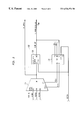
- FIG. 2 shows a block diagram of a fractional-N phase-locked loop 200 in accordance with an exemplary embodiment of the present invention.
- Phase detector (PD) 202 compares the phase IN of the input signal having frequency F IN to the phase OUT of the feedback signal and generates an error signal that indicates the magnitude of the difference between IN and OUT .
- Charge pump 204 generates an amount of charge equivalent to the error signal
- loop filter 206 operates as an integrator that accumulates the net charge from charge pump 204 to generate loop-filter voltage V LF applied to voltage-controlled oscillator (VCO) 208 .
- VCO 208 generates the output signal with frequency F OUT based on the loop-filter voltage V LF . As shown in FIG.
- VCO 208 is a ring oscillator having three inverting stages 216 a - 216 c, although a ring oscillator having more or fewer stages may be employed for VCO 208 .
- Input divider 210 may be placed in the input path and includes a count-by-R counter to divide a periodic input signal with frequency F IN by R.
- Multiplexer 214 and feedback divider 212 are placed in the feedback path, and feedback divider 212 includes a count-by-N counter to divide its input signal by N.
- feedback divider 212 uses signals generated by VCO 208 , feedback divider 212 generates the PLL feedback signal with phase OUT provided to the PD 202 .
- the ring oscillator of VCO 208 comprises an odd number of inverting stages 216 a - 216 c to provide the VCO output signal.
- a ring oscillator may comprise three CMOS inverters.
- the output signal of each stage has a periodic signal at the frequency of the ring oscillator but with a phase determined by the number of stages.
- Each stage provides its output signal with a different phase with respect to the other stages based on its position in the ring. Since the odd number of stages provide an odd number of signal phases, one or more non-inverting stages may be added to the ring oscillator to provide an even number of signal phases.
- the ring oscillator operates at a frequency determined by the delay through a single stage and by the number of stages. As shown in FIG.
- the output signal of one of the stages 216 a - 216 c (e.g., the output of the last stage 216 c ) is used as the output signal of the VCO 208 with frequency F OUT .
- the phases of the output signals from the stages 216 a - 216 c for the exemplary implementation shown in FIG. 2 (termed herein as output signal phases 1-3 ) are 120° out-of-phase with each other.
- output signal phases 1-3 are 120° out-of-phase with each other.
- one skilled in the art could extend the design of the ring oscillator to provide any phase difference desired with a combination of an odd number of inverting stages and, if necessary, one or more non-inverting stages.
- One or more signal phases 1-3 of the ring oscillator are provided to multiplexer (mux) 214 .
- One of the signal phases 1-3 of the ring oscillator is selected by the mux 214 based on a select (or “state”) signal of finite-state machine (FSM) 216 .
- the selected signal phase 1 , 2 , or 3 is used to clock the count-by-N counter of feedback divider 212 .
- FSM 216 After the counter has completed a full cycle (e.g., N counter increments) using one (i.e., the currently selected) signal phase of the ring oscillator, FSM 216 generates a state signal to mux 214 to select a different phase of the ring oscillator to clock the counter for the next count cycle.
- FSM 216 operates on an edge of the output signal of the counter.
- the phase 1 , 2 , or 3 selected by mux 214 advances or delays the start of the next count cycle by an amount substantially equivalent to the delay of a corresponding number of stages of the ring oscillator.
- the effective count of the counter of feedback divider 212 is (N+(1 ⁇ 3)).
- the effective count is (N ⁇ (1 ⁇ 3)) (i.e., the selected signal phase leads).
- the advance or delay selected with the mux 214 may be equivalent to one or more stage delays.
- FSM 216 generates the state signal based on the output signal of feedback divider 212 .
- FSM 216 may also receive one or more of the signal phases of the ring oscillator to generate a state signal having states corresponding to desired operation of the feedback divider.
- a control signal may also be employed to select the operation of the feedback divider to configure the PLL circuit as either a divide by N, or as a fractional-N PLL (with either leading or lagging signal phases).
- the exemplary implementation selectively divides the PLL output signal by either 11/3 or by 10/3 to generate the PLL feedback signal to PD 202 .
- the feedback divider When FIX is logic high, the feedback divider operates as a divide-by-4 to generate the PLL feedback signal (i.e., the PLL operates in a manner similar to the PLL shown in FIG. 1 ).
- FIG. 5 shows a corresponding timing diagram showing the selection of the signal phase 1-3 (VCOPH 1 -VCOPH 3 ) using the sequence of values of state signal (comprising SEL 1 and SEL 0 ) to provide overall divide by 11 ⁇ 3 in the PLL feedback path.
- the arrows in FIG. 5 indicate the transitions between the signal phases to clock the count-by-N counter that provides the fractional-N output count (PLL feedback signal) COUNT_OUT.
- FIG. 6 shows a circuit logic circuit schematic for the finite state machine shown in FIG. 3 implementing the state transition diagram of FIG. 4 using the control input values to generate the state signal (i.e., SEL 1 and SEL 0 ).
- a fractional-N PLL may be implemented in accordance with the present invention that maintains phase alignment of the phase detector while avoiding complex analog compensation circuitry. Since the delay added to starting the counter in the feedback path may be equivalent as each phase is selected, the PD 202 does not receive a disjoint signal from the feedback path that causes large, instantaneous phase errors such as encountered in fractional-N PLLs of the prior art.
- An exemplary implementation of the present invention may generate a 48-MHz output frequency from a 19.44-MHz input as follows.
- the input divider counter value R may be set to 27 and the feedback divider counter value N may be set to 662 ⁇ 3. Consequently, the phase detector operates at 720-KHz with near-ideal phase alignment. Operating a phase detector at a higher frequency simplifies the analog circuit design, allowing the use of a smaller loop filter capacitor and decreasing lock time of the PLL.
- circuit elements may also be implemented in the digital domain as processing steps in a software program.
- Such software may be employed in, for example, a digital signal processor, micro-controller or general purpose computer.
- the present invention can be embodied in the form of methods and apparatuses for practicing those methods.
- the present invention can also be embodied in the form of program code embodied in tangible media, such as floppy diskettes, CD-ROMs, hard drives, or any other machine-readable storage medium, wherein, when the program code is loaded into and executed by a machine, such as a computer, the machine becomes an apparatus for practicing the invention.
- the present invention can also be embodied in the form of program code, for example, whether stored in a storage medium, loaded into and/or executed by a machine, or transmitted over some transmission medium, such as over electrical wiring or cabling, through fiber optics, or via electromagnetic radiation, wherein, when the program code is loaded into and executed by a machine, such as a computer, the machine becomes an apparatus for practicing the invention.
- program code When implemented on a general-purpose processor, the program code segments combine with the processor to provide a unique device that operates analogously to specific logic circuits.
Abstract
Description

Claims (14)
Priority Applications (1)
| Application Number | Priority Date | Filing Date | Title |
|---|---|---|---|
| US09/460,169 US6526374B1 (en) | 1999-12-13 | 1999-12-13 | Fractional PLL employing a phase-selection feedback counter |
Applications Claiming Priority (1)
| Application Number | Priority Date | Filing Date | Title |
|---|---|---|---|
| US09/460,169 US6526374B1 (en) | 1999-12-13 | 1999-12-13 | Fractional PLL employing a phase-selection feedback counter |
Publications (1)
| Publication Number | Publication Date |
|---|---|
| US6526374B1 true US6526374B1 (en) | 2003-02-25 |
Family
ID=23827633
Family Applications (1)
| Application Number | Title | Priority Date | Filing Date |
|---|---|---|---|
| US09/460,169 Expired - Fee Related US6526374B1 (en) | 1999-12-13 | 1999-12-13 | Fractional PLL employing a phase-selection feedback counter |
Country Status (1)
| Country | Link |
|---|---|
| US (1) | US6526374B1 (en) |
Cited By (13)
| Publication number | Priority date | Publication date | Assignee | Title |
|---|---|---|---|---|
| US20040252805A1 (en) * | 2001-07-06 | 2004-12-16 | Van Zeijl Paulus Thomas M. | Fractional frequency divider |
| US20050134337A1 (en) * | 2003-12-22 | 2005-06-23 | Micron Technology, Inc. | Clock signal distribution with reduced parasitic loading effects |
| US20050206417A1 (en) * | 2002-06-19 | 2005-09-22 | Dominique Morche | Delay-locked loop |
| US20060055422A1 (en) * | 2004-09-15 | 2006-03-16 | Jason Gonzalez | Low power CMOS switching |
| US20060132200A1 (en) * | 2004-12-22 | 2006-06-22 | Markus Dietl | Fractional-N divider, fractional-N phase locked loop and method of dividing a frequency f of an output signal by N, wherein N is a non-integer |
| US20070247202A1 (en) * | 2006-04-20 | 2007-10-25 | Chia-Liang Lin | Variable delay clock circuit and method thereof |
| WO2008145703A1 (en) * | 2007-05-30 | 2008-12-04 | Texas Instruments Deutschland Gmbh | Register with process, supply voltage and temperature variation independent propagation delay path |
| US7545188B1 (en) * | 2006-08-04 | 2009-06-09 | Integrated Device Technology, Inc | Multiphase clock generator |
| US20110025382A1 (en) * | 2009-07-28 | 2011-02-03 | Nxp B.V. | Frequency divider |
| DE102005050828B4 (en) * | 2004-12-22 | 2011-08-18 | Texas Instruments Deutschland GmbH, 85356 | Method and apparatus for dividing a frequency by a fractional divider and fractional-n PLL |
| EP3033833A4 (en) * | 2014-03-12 | 2017-03-08 | MediaTek Singapore Pte Ltd. | Divisor control circuit, fractional frequency division device, frequency synthesizer and frequency synthesis method |
| EP3208943A1 (en) * | 2004-03-05 | 2017-08-23 | Telefonaktiebolaget LM Ericsson (publ) | Fractional frequency synthesizer |
| US20180076821A1 (en) * | 2016-09-09 | 2018-03-15 | Samsung Electronics Co., Ltd. | System and method of calibrating input signal to successive approximation register (sar) analog-to-digital converter (adc) in adc-assisted time-to-digital converter (tdc) |
Citations (6)
| Publication number | Priority date | Publication date | Assignee | Title |
|---|---|---|---|---|
| US5727038A (en) * | 1996-09-06 | 1998-03-10 | Motorola, Inc. | Phase locked loop using digital loop filter and digitally controlled oscillator |
| US5889436A (en) * | 1996-11-01 | 1999-03-30 | National Semiconductor Corporation | Phase locked loop fractional pulse swallowing frequency synthesizer |
| US6075395A (en) * | 1997-05-30 | 2000-06-13 | Nec Corporation | Synchronous delay circuit |
| US6114914A (en) * | 1999-05-19 | 2000-09-05 | Cypress Semiconductor Corp. | Fractional synthesis scheme for generating periodic signals |
| US6380774B2 (en) * | 2000-03-24 | 2002-04-30 | Nec Corporation | Clock control circuit and clock control method |
| US6396320B2 (en) * | 1998-06-12 | 2002-05-28 | Nec Corporation | Clock control method and circuit |
-
1999
- 1999-12-13 US US09/460,169 patent/US6526374B1/en not_active Expired - Fee Related
Patent Citations (6)
| Publication number | Priority date | Publication date | Assignee | Title |
|---|---|---|---|---|
| US5727038A (en) * | 1996-09-06 | 1998-03-10 | Motorola, Inc. | Phase locked loop using digital loop filter and digitally controlled oscillator |
| US5889436A (en) * | 1996-11-01 | 1999-03-30 | National Semiconductor Corporation | Phase locked loop fractional pulse swallowing frequency synthesizer |
| US6075395A (en) * | 1997-05-30 | 2000-06-13 | Nec Corporation | Synchronous delay circuit |
| US6396320B2 (en) * | 1998-06-12 | 2002-05-28 | Nec Corporation | Clock control method and circuit |
| US6114914A (en) * | 1999-05-19 | 2000-09-05 | Cypress Semiconductor Corp. | Fractional synthesis scheme for generating periodic signals |
| US6380774B2 (en) * | 2000-03-24 | 2002-04-30 | Nec Corporation | Clock control circuit and clock control method |
Non-Patent Citations (1)
| Title |
|---|
| "Charge-Pump Phase-Lock Loops," by Floyd M. Gardner, IEEE Trans. Commun. vol. COM-28, No. 11, Nov. 1980, pp. 321-329. |
Cited By (25)
| Publication number | Priority date | Publication date | Assignee | Title |
|---|---|---|---|---|
| US7084678B2 (en) * | 2001-07-06 | 2006-08-01 | Telefonaktiebolaget Lm Ericsson (Publ) | Fractional frequency divider |
| US20040252805A1 (en) * | 2001-07-06 | 2004-12-16 | Van Zeijl Paulus Thomas M. | Fractional frequency divider |
| US20050206417A1 (en) * | 2002-06-19 | 2005-09-22 | Dominique Morche | Delay-locked loop |
| US7391244B2 (en) * | 2002-06-19 | 2008-06-24 | Commissariat A L'energie Atomique | Delay-locked loop |
| US7528638B2 (en) * | 2003-12-22 | 2009-05-05 | Micron Technology, Inc. | Clock signal distribution with reduced parasitic loading effects |
| US20050134337A1 (en) * | 2003-12-22 | 2005-06-23 | Micron Technology, Inc. | Clock signal distribution with reduced parasitic loading effects |
| EP3208943A1 (en) * | 2004-03-05 | 2017-08-23 | Telefonaktiebolaget LM Ericsson (publ) | Fractional frequency synthesizer |
| US7053651B2 (en) * | 2004-09-15 | 2006-05-30 | Avago Technologies General Ip Pte. Ltd. | Low power CMOS switching |
| US20060055422A1 (en) * | 2004-09-15 | 2006-03-16 | Jason Gonzalez | Low power CMOS switching |
| DE102005050828B4 (en) * | 2004-12-22 | 2011-08-18 | Texas Instruments Deutschland GmbH, 85356 | Method and apparatus for dividing a frequency by a fractional divider and fractional-n PLL |
| US20060132200A1 (en) * | 2004-12-22 | 2006-06-22 | Markus Dietl | Fractional-N divider, fractional-N phase locked loop and method of dividing a frequency f of an output signal by N, wherein N is a non-integer |
| US20070247202A1 (en) * | 2006-04-20 | 2007-10-25 | Chia-Liang Lin | Variable delay clock circuit and method thereof |
| US7405604B2 (en) * | 2006-04-20 | 2008-07-29 | Realtek Semiconductor Corp. | Variable delay clock circuit and method thereof |
| US7545188B1 (en) * | 2006-08-04 | 2009-06-09 | Integrated Device Technology, Inc | Multiphase clock generator |
| WO2008145703A1 (en) * | 2007-05-30 | 2008-12-04 | Texas Instruments Deutschland Gmbh | Register with process, supply voltage and temperature variation independent propagation delay path |
| US8111092B2 (en) | 2007-05-30 | 2012-02-07 | Texas Instruments Incorporated | Register with process, supply voltage and temperature variation independent propagation delay path |
| US20080301485A1 (en) * | 2007-05-30 | 2008-12-04 | Texas Instruments Deutschland Gmbh | Register with process, supply voltage and temperature variation independent propagation delay path |
| EP2288031A1 (en) | 2009-07-28 | 2011-02-23 | Nxp B.V. | A frequency divider |
| US20110025382A1 (en) * | 2009-07-28 | 2011-02-03 | Nxp B.V. | Frequency divider |
| EP3033833A4 (en) * | 2014-03-12 | 2017-03-08 | MediaTek Singapore Pte Ltd. | Divisor control circuit, fractional frequency division device, frequency synthesizer and frequency synthesis method |
| CN106537782A (en) * | 2014-03-12 | 2017-03-22 | 联发科技(新加坡)私人有限公司 | Divisor control circuit, fractional frequency division device, frequency synthesizer and frequency synthesis method |
| US20180076821A1 (en) * | 2016-09-09 | 2018-03-15 | Samsung Electronics Co., Ltd. | System and method of calibrating input signal to successive approximation register (sar) analog-to-digital converter (adc) in adc-assisted time-to-digital converter (tdc) |
| US10009036B2 (en) * | 2016-09-09 | 2018-06-26 | Samsung Electronics Co., Ltd | System and method of calibrating input signal to successive approximation register (SAR) analog-to-digital converter (ADC) in ADC-assisted time-to-digital converter (TDC) |
| US10623010B2 (en) * | 2016-09-09 | 2020-04-14 | Samsung Electronics Co., Ltd | System and method of calibrating input signal to successive approximation register (SAR) analog-to-digital converter (ADC) in ADC-assisted time-to- digital converter (TDC) |
| TWI723182B (en) * | 2016-09-09 | 2021-04-01 | 南韓商三星電子股份有限公司 | Apparatus, method of calibrating, method of manufacturing apparatus, and method of constructing an integrated circuit |
Similar Documents
| Publication | Publication Date | Title |
|---|---|---|
| US6208183B1 (en) | Gated delay-locked loop for clock generation applications | |
| US9503109B2 (en) | Apparatus and methods for synchronizing phase-locked loops | |
| US6310498B1 (en) | Digital phase selection circuitry and method for reducing jitter | |
| EP2757692B1 (en) | Synthesizer with lock detector and method of operation thereof | |
| EP1022857A2 (en) | Phase locked loop and method that provide fail-over redundant clocking | |
| US6526374B1 (en) | Fractional PLL employing a phase-selection feedback counter | |
| US6150889A (en) | Circuit and method for minimizing recovery time | |
| EP1323233A2 (en) | Synchornized mutli-output digital clock manager | |
| WO1987001885A1 (en) | Phase comparator lock detect circuit and a synthesiser using same | |
| US6909329B2 (en) | Adaptive loop bandwidth circuit for a PLL | |
| CN111149299B (en) | System-on-chip clock phase management using fractional-N PLLs | |
| US7323942B2 (en) | Dual loop PLL, and multiplication clock generator using dual loop PLL | |
| US20020057118A1 (en) | Apparatus and method for counting high-speed early/late pulses from a high speed phase detector using a pulse accumulator | |
| US20050030001A1 (en) | PLL employing a sample-based capacitance multiplier | |
| JP7324013B2 (en) | Fractional divider and frequency synthesizer | |
| EP2571165B1 (en) | Accumulator type fractional-n pll synthesizer and control method thereof | |
| CN113497620A (en) | Clock data recovery circuit and multiplexer circuit | |
| US6970047B1 (en) | Programmable lock detector and corrector | |
| US8866556B2 (en) | Phase shift phase locked loop | |
| EP2659589A1 (en) | Phase-frequency detection method | |
| US8035451B2 (en) | On-the-fly frequency switching while maintaining phase and frequency lock | |
| JP4015254B2 (en) | Lock detection circuit and PLL frequency synthesizer | |
| EP1662663B1 (en) | PLL circuit | |
| US20050057314A1 (en) | Device and method for detecting phase difference and PLL using the same | |
| US7298809B2 (en) | Self-calibration of a PLL with multiphase clocks |
Legal Events
| Date | Code | Title | Description |
|---|---|---|---|
| AS | Assignment |
Owner name: LUCENT TECHNOLOGIES INC., NEW JERSEY Free format text: ASSIGNMENT OF ASSIGNORS INTEREST;ASSIGNOR:MARTIN, DAVID G.;REEL/FRAME:010479/0883 Effective date: 19991209 |
|
| FEPP | Fee payment procedure |
Free format text: PAYOR NUMBER ASSIGNED (ORIGINAL EVENT CODE: ASPN); ENTITY STATUS OF PATENT OWNER: LARGE ENTITY |
|
| FPAY | Fee payment |
Year of fee payment: 4 |
|
| FPAY | Fee payment |
Year of fee payment: 8 |
|
| AS | Assignment |
Owner name: DEUTSCHE BANK AG NEW YORK BRANCH, AS COLLATERAL AG Free format text: PATENT SECURITY AGREEMENT;ASSIGNORS:LSI CORPORATION;AGERE SYSTEMS LLC;REEL/FRAME:032856/0031 Effective date: 20140506 |
|
| REMI | Maintenance fee reminder mailed | ||
| LAPS | Lapse for failure to pay maintenance fees | ||
| STCH | Information on status: patent discontinuation |
Free format text: PATENT EXPIRED DUE TO NONPAYMENT OF MAINTENANCE FEES UNDER 37 CFR 1.362 |
|
| AS | Assignment |
Owner name: AVAGO TECHNOLOGIES GENERAL IP (SINGAPORE) PTE. LTD Free format text: ASSIGNMENT OF ASSIGNORS INTEREST;ASSIGNOR:AGERE SYSTEMS LLC;REEL/FRAME:035365/0634 Effective date: 20140804 |
|
| FP | Lapsed due to failure to pay maintenance fee |
Effective date: 20150225 |
|
| AS | Assignment |
Owner name: LSI CORPORATION, CALIFORNIA Free format text: TERMINATION AND RELEASE OF SECURITY INTEREST IN PATENT RIGHTS (RELEASES RF 032856-0031);ASSIGNOR:DEUTSCHE BANK AG NEW YORK BRANCH, AS COLLATERAL AGENT;REEL/FRAME:037684/0039 Effective date: 20160201 Owner name: AGERE SYSTEMS LLC, PENNSYLVANIA Free format text: TERMINATION AND RELEASE OF SECURITY INTEREST IN PATENT RIGHTS (RELEASES RF 032856-0031);ASSIGNOR:DEUTSCHE BANK AG NEW YORK BRANCH, AS COLLATERAL AGENT;REEL/FRAME:037684/0039 Effective date: 20160201 |