US6535407B1 - DC/DC converter having a piezoelectric transformer and rectification-smoothing circuit - Google Patents
DC/DC converter having a piezoelectric transformer and rectification-smoothing circuit Download PDFInfo
- Publication number
- US6535407B1 US6535407B1 US09/123,522 US12352298A US6535407B1 US 6535407 B1 US6535407 B1 US 6535407B1 US 12352298 A US12352298 A US 12352298A US 6535407 B1 US6535407 B1 US 6535407B1
- Authority
- US
- United States
- Prior art keywords
- fet
- piezoelectric transformer
- rectification
- terminal
- inductor
- Prior art date
- Legal status (The legal status is an assumption and is not a legal conclusion. Google has not performed a legal analysis and makes no representation as to the accuracy of the status listed.)
- Expired - Fee Related
Links
Images


Classifications
-
- H—ELECTRICITY
- H02—GENERATION; CONVERSION OR DISTRIBUTION OF ELECTRIC POWER
- H02M—APPARATUS FOR CONVERSION BETWEEN AC AND AC, BETWEEN AC AND DC, OR BETWEEN DC AND DC, AND FOR USE WITH MAINS OR SIMILAR POWER SUPPLY SYSTEMS; CONVERSION OF DC OR AC INPUT POWER INTO SURGE OUTPUT POWER; CONTROL OR REGULATION THEREOF
- H02M3/00—Conversion of dc power input into dc power output
- H02M3/22—Conversion of dc power input into dc power output with intermediate conversion into ac
- H02M3/24—Conversion of dc power input into dc power output with intermediate conversion into ac by static converters
- H02M3/28—Conversion of dc power input into dc power output with intermediate conversion into ac by static converters using discharge tubes with control electrode or semiconductor devices with control electrode to produce the intermediate ac
- H02M3/325—Conversion of dc power input into dc power output with intermediate conversion into ac by static converters using discharge tubes with control electrode or semiconductor devices with control electrode to produce the intermediate ac using devices of a triode or a transistor type requiring continuous application of a control signal
- H02M3/335—Conversion of dc power input into dc power output with intermediate conversion into ac by static converters using discharge tubes with control electrode or semiconductor devices with control electrode to produce the intermediate ac using devices of a triode or a transistor type requiring continuous application of a control signal using semiconductor devices only
- H02M3/33569—Conversion of dc power input into dc power output with intermediate conversion into ac by static converters using discharge tubes with control electrode or semiconductor devices with control electrode to produce the intermediate ac using devices of a triode or a transistor type requiring continuous application of a control signal using semiconductor devices only having several active switching elements
- H02M3/33576—Conversion of dc power input into dc power output with intermediate conversion into ac by static converters using discharge tubes with control electrode or semiconductor devices with control electrode to produce the intermediate ac using devices of a triode or a transistor type requiring continuous application of a control signal using semiconductor devices only having several active switching elements having at least one active switching element at the secondary side of an isolation transformer
- H02M3/33592—Conversion of dc power input into dc power output with intermediate conversion into ac by static converters using discharge tubes with control electrode or semiconductor devices with control electrode to produce the intermediate ac using devices of a triode or a transistor type requiring continuous application of a control signal using semiconductor devices only having several active switching elements having at least one active switching element at the secondary side of an isolation transformer having a synchronous rectifier circuit or a synchronous freewheeling circuit at the secondary side of an isolation transformer
-
- H—ELECTRICITY
- H02—GENERATION; CONVERSION OR DISTRIBUTION OF ELECTRIC POWER
- H02M—APPARATUS FOR CONVERSION BETWEEN AC AND AC, BETWEEN AC AND DC, OR BETWEEN DC AND DC, AND FOR USE WITH MAINS OR SIMILAR POWER SUPPLY SYSTEMS; CONVERSION OF DC OR AC INPUT POWER INTO SURGE OUTPUT POWER; CONTROL OR REGULATION THEREOF
- H02M3/00—Conversion of dc power input into dc power output
- H02M3/22—Conversion of dc power input into dc power output with intermediate conversion into ac
- H02M3/24—Conversion of dc power input into dc power output with intermediate conversion into ac by static converters
- H02M3/28—Conversion of dc power input into dc power output with intermediate conversion into ac by static converters using discharge tubes with control electrode or semiconductor devices with control electrode to produce the intermediate ac
- H02M3/325—Conversion of dc power input into dc power output with intermediate conversion into ac by static converters using discharge tubes with control electrode or semiconductor devices with control electrode to produce the intermediate ac using devices of a triode or a transistor type requiring continuous application of a control signal
- H02M3/335—Conversion of dc power input into dc power output with intermediate conversion into ac by static converters using discharge tubes with control electrode or semiconductor devices with control electrode to produce the intermediate ac using devices of a triode or a transistor type requiring continuous application of a control signal using semiconductor devices only
- H02M3/33569—Conversion of dc power input into dc power output with intermediate conversion into ac by static converters using discharge tubes with control electrode or semiconductor devices with control electrode to produce the intermediate ac using devices of a triode or a transistor type requiring continuous application of a control signal using semiconductor devices only having several active switching elements
- H02M3/33571—Half-bridge at primary side of an isolation transformer
-
- Y—GENERAL TAGGING OF NEW TECHNOLOGICAL DEVELOPMENTS; GENERAL TAGGING OF CROSS-SECTIONAL TECHNOLOGIES SPANNING OVER SEVERAL SECTIONS OF THE IPC; TECHNICAL SUBJECTS COVERED BY FORMER USPC CROSS-REFERENCE ART COLLECTIONS [XRACs] AND DIGESTS
- Y02—TECHNOLOGIES OR APPLICATIONS FOR MITIGATION OR ADAPTATION AGAINST CLIMATE CHANGE
- Y02B—CLIMATE CHANGE MITIGATION TECHNOLOGIES RELATED TO BUILDINGS, e.g. HOUSING, HOUSE APPLIANCES OR RELATED END-USER APPLICATIONS
- Y02B70/00—Technologies for an efficient end-user side electric power management and consumption
- Y02B70/10—Technologies improving the efficiency by using switched-mode power supplies [SMPS], i.e. efficient power electronics conversion e.g. power factor correction or reduction of losses in power supplies or efficient standby modes
Definitions
- the present invention relates to a DC/DC converter and in particular, to a high-efficiency DC/DC converter using a piezoelectric transformer.
- JP Patent, Publication of Unexamined Application A-7-59338 [B] suggests a piezoelectric transformer having a three-terminal output configuration in which a piezoelectric transformer output block (secondary side) has an intermediate tap for taking out an intermediate voltage so that the rectifier forward voltage drop is V F .
- a piezoelectric transformer output block secondary side
- an intermediate tap for taking out an intermediate voltage so that the rectifier forward voltage drop is V F .
- FIG. 1 of document [B] it is possible to easily constitute a rectifier circuit having a diode forward voltage drop of V F .
- a power source circuit having a current doubler Double Ended Converter using Two Inductors
- the first problem is that in the aforementioned first conventional example, i.e., the piezoelectric transformer of two-terminal output as described in document [A], rectification is carried out by a bridge rectification circuit and accordingly a diode forward voltage drop of 2 V F is caused. If the output voltage is as low as 10 V, a loss is significantly remarkable, lowering the efficiency.
- the second problem is that the aforementioned second conventional example, i.e., the piezoelectric transformer having a center tap as disclosed in document [B] requires a production process of a high accuracy for providing the center tap. That is, it is not easy to produce such a configuration and a production cost is increased.
- the rectification-smoothing circuit is realized as a rectification-smoothing circuit using a current doubler.
- the diode rectification is replaced by a synchronous rectification.
- a gate waveform rectification circuit is used for clamping a piezoelectric transformer output voltage as a sinusoidal wave so as to maintain a constant gate voltage.
- the present invention by using a two-terminal output type piezoelectric transformer in combination with a current doubler rectification-smoothing circuit, it is possible to make the diode forward voltage drop VF and to reduce the loss compared to the bridge rectification.
- a synchronous rectification FET is used instead of a diode in the current doubler rectification-smoothing circuit, in a range V F >Io ⁇ Ron (wherein Io is an output current, and Ron is a FET ‘ON’ resistance), the synchronous rectification FET can reduce the loss more than the diode.
- the piezoelectric transformer has a strong resonance characteristic and accordingly, for any input waveforms (for example, square waveform, triangle waveform, or sinusoidal waveform), the piezoelectric transformer output voltage has a sinusoidal waveform. Consequently, if the piezoelectric transformer output voltage is directly used as a synchronous rectification FET gate signal, the output sinusoidal wave voltage has a peak value exceeding an absolute maximum rating (usually, 20 V) of the synchronous rectification FET gate, which may destroy the synchronous rectification FET.
- an absolute maximum rating usually, 20 V
- the piezoelectric transformer output sinusoidal wave voltage has a peak value set to a sufficiently low value not to exceed the gate absolute maximum rating, it becomes impossible to obtain a sufficiently long period of time for exceeding the gate ‘ON’ voltage threshold value V TH and accordingly, the synchronous rectification FET cannot be in ‘ON’ state for a sufficiently long period of time.
- a solution to this problem is clamping with an appropriate value (such as 10 V) the piezoelectric transformer output sinusoidal wave voltage having a sufficiently great peak value. This can be realized by using a gate waveform rectification circuit.
- FIG. 1 is a block diagram showing a basic circuit configuration according to the present invention.
- FIG. 2A, FIG. 2B, and FIG. 2C are block diagrams showing variations of a switching circuit used in the present invention.
- FIG. 3 is a block diagram showing a circuit configuration according to a first embodiment of the present invention.
- FIG. 4 is a timing chart showing waveforms involved in the circuit according to the first embodiment shown in FIG. 3 .
- FIG. 5 is a block diagram for explanation of operation of a current doubler rectification-smoothing circuit.
- FIG. 6 is a block diagram showing a circuit configuration of a piezoelectric transformer DC/DC converter using a current doubler rectification-smoothing circuit of synchronous rectification type according to a second embodiment of the present invention.
- FIG. 7 shows a gate waveform (observed) of FET for synchronous rectification.
- FIG. 8 is a block diagram showing an essential portion of a first modification of the second embodiment.
- FIG. 9 is a block diagram showing an essential portion of a second modification of the second embodiment.
- FIG. 10 is a block diagram showing an essential portion of a third modification of the second embodiment.
- FIG. 11 is a block diagram showing a circuit configuration according to a third embodiment of the present invention.
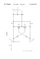
- FIG. 1 is a block diagram showing a representative circuit configuration according to the present invention.
- the circuit according to the present invention basically includes a DC input power source 1 , a switching circuit 2 , a piezoelectric transformer 3 , a current doubler rectification-smoothing circuit 4 , and a load resistor 5 .
- the switching circuit 2 may be a half-bridge type shown in FIG. 2A, an active clamp type shown in FIG. 2B, an E class resonance type, or any other type.
- FIG. 3 shows a specific example of the circuit configuration of FIG. 1 according to the first embodiment.
- the piezoelectric transformer 3 is represented by an equivalent circuit, and the switching circuit is realized as the half-bridge type shown in FIG. 2A as a representative circuit.
- a charge/discharge inductor 16 and a DC bias cut capacitor 15 are added to the half-bridge type switching circuit.
- the switching circuit 2 has switches 11 and 12 which are driven by gate voltage vG 1 and vG 2 having a dead time so as to be alternately turned ON and OFF.
- the input capacitor 17 of the piezoelectric transformer 3 is charged and discharged by an inductor current flowing through an inductor 16 . Consequently, the piezoelectric transformer 3 has an input voltage waveform v 1 which is a quasi-square waveform as shown in FIG. 4 .
- This input voltage v 1 is applied to the piezoelectric transformer 3 having a strong band-pass filter characteristic and accordingly, a sinusoidal wave ir flows inside the piezoelectric transformer 3 so that the piezoelectric transformer 3 has an output voltage waveform which is a sinusoidal wave v 2 .
- V 2 is an amplitude of v 2 .
- An output current i 2 from the piezoelectric transformer 3 flows with an amplitude of ⁇ I 0 /2, wherein I 0 represents an output current flowing through a load resistor 5 .
- the diode 6 is ‘OFF’.
- the output current i 2 from the piezoelectric transformer 3 flows through the inductor 8 and the diode 7 and supplies a power to the load resistor 5 .
- the inductor 8 half of the load current, i.e., +I 0 /2 is flowing. Simultaneously with this, another +I 0 /2 current flows to the inductor 9 via the diode 7 and the load resistor 5 as a circulating current like a free wheel. This current of the inductor 8 is added to the current of the inductor 9 to make a load current I 0 .
- Each of the currents flowing to the inductors 8 and 9 is overlaid with a ripple current which is determined by an inductance. However, the ripple currents are cancelled because of having a reversed phase to each other, and almost no ripple current flows into the output capacitor 10 .
- the piezoelectric transformer in combination with a current doubler In an ordinary current doubler, where the time ratio of the positive and negative half cycles may not be equal to each other, it is impossible to completely cancel such ripple currents. That is, as ripple currents flow into the capacitor 10 , the capacitor 10 need to have a sufficiently great capacitance.
- the output of the piezoelectric transformer is always a sinusoidal wave and the time ratio of the positive and the negative half cycles are always identical.
- the output capacitor 10 may have a small capacitance. Because it is possible to make the inductance of the inductors 8 and 9 small, this can contribute to reduction of the entire converter apparatus.
- the diode 7 In the negative half cycle [tA ⁇ tB], the diode 7 is OFF.
- the output current i 2 flows through the inductor 9 and the diode 6 for supplying a power to the load resistor 5 .
- the operation involved here is identical to the operation explained in the aforementioned positive half cycle.
- FIG. 6 is a block diagram showing a circuit configuration according to the second embodiment.
- the input side to the piezoelectric transformer 3 is identical as in FIG. 3 and it is omitted in this FIG. 6 .
- the aforementioned diodes 6 and 7 in the first embodiment are respectively replaced by a synchronous rectification FET 23 and a synchronous rectification FET 24 .
- the FET 23 has a gate terminal connected via a waveform rectification circuit 25 to an output terminal ‘a’ of the piezoelectric transformer 3 .
- the FET 24 has a gate terminal connected via the waveform rectification circuit 25 to an output terminal ‘b’ of the piezoelectric transformer 3 .
- the synchronous rectification FET 23 has a gate terminal connected to a source of a clamp FET 26 .
- the FET 26 has a drain connected to the output terminal ‘b’ of the piezoelectric transformer 3 , and a gate terminal connected to a clamp voltage source 28 .
- the synchronous rectification FET 24 has a gate terminal connected to a source of the clamp FET 27 , whose drain is connected to the output terminal ‘a’ of the piezoelectric transformer 3 and whose gate is connected to the clamp voltage source 28 .
- the output voltage v 2 of the piezoelectric transformer 3 becomes positive.
- the clamp FET 27 has been turned ON by the clamp voltage Vb of the clamp voltage source 28 applied to the gate. Accordingly, the FET 27 has a source voltage v 3 which is also positive and equal to the output voltage v 2 .
- the FET 27 is turned OFF and the source voltage v 3 becomes equal to the clamp voltage Vb as a constant voltage.
- the clamp voltage Vb is set to an appropriate value in the order of 10 V.
- the negative half cycle operates identically.
- FIG. 8, FIG. 9, and FIG. 10 show modifications of the synchronous rectification type current doubler rectification-smoothing circuit according to the second embodiment.
- the clamp voltage source 28 is removed and the clamp voltage Vb is supplied from the output voltage of the converter.
- the circuit configuration of FIG. 8 differs from the circuit configuration of FIG. 9 in that the clamp voltage source 28 is removed and that instead of using the voltage Vb, the gate terminals of FET 26 and FET 27 are connected to the output of the DC/DC converter. Thus, it is possible to reduce the number of components constituting the circuit.
- the synchronous rectification FET 23 has a gate terminal connected via a zener diode 29 to the output terminal ‘a’ of the piezoelectric transformer 3
- the synchronous rectification FET 24 has a gate terminal connected via a zener diode 30 to the output terminal ‘a’ of the piezoelectric transformer 3 .
- the circuit of FIG. 9 differs from the circuit of FIG. 6 and FIG. 8 in that the FET 26 and FET 27 are replaced by zener diodes 29 and 30 . That is, it is possible to reduce a production cost of the entire configuration.
- the synchronous rectification FET 2 has a gate terminal connected via a bias cut capacitor 31 to the output terminal ‘b’ of the piezoelectric transformer 3
- the synchronous rectification FET 24 has a gate terminal connected via a bias cut capacitor 32 to the output terminal ‘a’ of the piezoelectric transformer 3 .
- FIG. 10 differs from that of FIG. 6 and FIG. 8 in that the FETs are replaced by the capacitors. Accordingly, in the same way as the aforementioned modification of FIG. 9, it is possible to reduce the production cost of the entire circuit.
- FIG. 11 shows a circuit configuration according to the third embodiment of the present invention.
- a second winding is provided to the resonance inductor 16 of FIG. 3 so as to constitute a resonance inductor 33 , so that an AC voltage induced by this second winding is converted into a DC voltage by the rectification-smoothing circuit 34 for use as a power voltage of the control IC 35 .
- the DC/DC converters according to the first, the second, and the third embodiments have been explained for DC power source as an input, but can also be applied directly to a so-called AC input power source in which an AC input (such as 100 VAC/50 Hz) is rectified-smoothed into a DC voltage.
- an AC input such as 100 VAC/50 Hz
- the present invention has various effects as follows.
Abstract
A DC/DC converter is provided that includes a switch device for converting a DC voltage into an AC voltage, a piezoelectric transformer for changing the AC voltage and a current doubler type rectification-smoothing device, which includes a first diode, a second diode, a first inductor, a second inductor, and a capacitor. The piezoelectric transformer has one output terminal connected to a cathode of the first diode and to one terminal of the first inductor, and the other output terminal connected to a cathode of the second diode and to one terminal of the second inductor. Anodes of the first and the second diodes are respectively grounded. The other terminal of the first inductor is connected at a predetermined connection point to the other terminal of the second inductor. The connection point is connected to one terminal of the capacitor, whose other terminal is grounded.
Description
1. Field of the Invention
The present invention relates to a DC/DC converter and in particular, to a high-efficiency DC/DC converter using a piezoelectric transformer.
2. Description of the Related Art
Conventionally, this type of technology used four-diode bridge rectification for rectification of a piezoelectric transformer of two-terminal output as a first conventional example described in “New Piezoelectric Transformer Converter for AC-adapter,” IEEE APEC97 (Applied Power Electronics Conference 97), pp. 568-572, FIG. 4 [A]. By using the bridge rectification, both of a positive half cycle and a negative half cycle can supply power to the load.
In the aforementioned FIG. 4 of document [A], if the diode voltage drop in the forward direction is VF, the diode forward direction voltage drop is 2 VF because two diodes are connected in series in each cycle.
On the other hand, as a second conventional example, JP Patent, Publication of Unexamined Application A-7-59338 [B] suggests a piezoelectric transformer having a three-terminal output configuration in which a piezoelectric transformer output block (secondary side) has an intermediate tap for taking out an intermediate voltage so that the rectifier forward voltage drop is VF. When such an intermediate tap is provided, as shown in FIG. 1 of document [B], it is possible to easily constitute a rectifier circuit having a diode forward voltage drop of VF. Moreover, a power source circuit having a current doubler (Double Ended Converter using Two Inductors) is disclosed in US Pat. No. 4,899,271, Specification [C] and JP Patent, Publication of Examined Application B-61-24913 (power source circuit) [D]. Furthermore, JP Patent, Publication of Unexamined Application A-5-284734 discloses a switching power source with a reduced loss in a rectification element, enabling to obtain an improved power conversion efficiency.
However, the aforementioned prior arts have various problems as follows.
The first problem is that in the aforementioned first conventional example, i.e., the piezoelectric transformer of two-terminal output as described in document [A], rectification is carried out by a bridge rectification circuit and accordingly a diode forward voltage drop of 2 VF is caused. If the output voltage is as low as 10 V, a loss is significantly remarkable, lowering the efficiency.
The second problem is that the aforementioned second conventional example, i.e., the piezoelectric transformer having a center tap as disclosed in document [B] requires a production process of a high accuracy for providing the center tap. That is, it is not easy to produce such a configuration and a production cost is increased.
It is therefore an object of the present invention to provide a novel DC/DC converter using a two-terminal piezoelectric transformer of reasonable cost and capable of reducing a rectification circuit loss and enhancing the power conversion efficiency.
In order to achieve the aforementioned object, in the DC/DC converter using a piezoelectric transformer, the rectification-smoothing circuit is realized as a rectification-smoothing circuit using a current doubler.
Furthermore, in the DC/DC converter using a piezoelectric transformer according to the present invention, in order to reduce the loss of the rectification circuit, the diode rectification is replaced by a synchronous rectification. Here, in order to assure drive of the rectification FET (field effect transistor), a gate waveform rectification circuit is used for clamping a piezoelectric transformer output voltage as a sinusoidal wave so as to maintain a constant gate voltage.
According to the present invention, by using a two-terminal output type piezoelectric transformer in combination with a current doubler rectification-smoothing circuit, it is possible to make the diode forward voltage drop VF and to reduce the loss compared to the bridge rectification.
If a synchronous rectification FET is used instead of a diode in the current doubler rectification-smoothing circuit, in a range VF>Io·Ron (wherein Io is an output current, and Ron is a FET ‘ON’ resistance), the synchronous rectification FET can reduce the loss more than the diode.
Here, in the present invention, for driving the synchronous rectification FET, a technique is devised to fully utilize a switching power source using a piezoelectric transformer. That is, the piezoelectric transformer has a strong resonance characteristic and accordingly, for any input waveforms (for example, square waveform, triangle waveform, or sinusoidal waveform), the piezoelectric transformer output voltage has a sinusoidal waveform. Consequently, if the piezoelectric transformer output voltage is directly used as a synchronous rectification FET gate signal, the output sinusoidal wave voltage has a peak value exceeding an absolute maximum rating (usually, 20 V) of the synchronous rectification FET gate, which may destroy the synchronous rectification FET. On the contrary, if the piezoelectric transformer output sinusoidal wave voltage has a peak value set to a sufficiently low value not to exceed the gate absolute maximum rating, it becomes impossible to obtain a sufficiently long period of time for exceeding the gate ‘ON’ voltage threshold value V TH and accordingly, the synchronous rectification FET cannot be in ‘ON’ state for a sufficiently long period of time.
A solution to this problem is clamping with an appropriate value (such as 10 V) the piezoelectric transformer output sinusoidal wave voltage having a sufficiently great peak value. This can be realized by using a gate waveform rectification circuit.
This enables to overcome the defect that the piezoelectric transformer output voltage is a sinusoidal wave and effectively operate the current doubler rectification-smoothing circuit of synchronous rectification type.
FIG. 1 is a block diagram showing a basic circuit configuration according to the present invention.
FIG. 2A, FIG. 2B, and FIG. 2C are block diagrams showing variations of a switching circuit used in the present invention.
FIG. 3 is a block diagram showing a circuit configuration according to a first embodiment of the present invention.
FIG. 4 is a timing chart showing waveforms involved in the circuit according to the first embodiment shown in FIG. 3.
FIG. 5 is a block diagram for explanation of operation of a current doubler rectification-smoothing circuit.
FIG. 6 is a block diagram showing a circuit configuration of a piezoelectric transformer DC/DC converter using a current doubler rectification-smoothing circuit of synchronous rectification type according to a second embodiment of the present invention.
FIG. 7 shows a gate waveform (observed) of FET for synchronous rectification.
FIG. 8 is a block diagram showing an essential portion of a first modification of the second embodiment.
FIG. 9 is a block diagram showing an essential portion of a second modification of the second embodiment.
FIG. 10 is a block diagram showing an essential portion of a third modification of the second embodiment.
FIG. 11 is a block diagram showing a circuit configuration according to a third embodiment of the present invention.
Description will now be directed to preferred embodiments of the present invention with reference to the attached drawings.
FIG. 1 is a block diagram showing a representative circuit configuration according to the present invention.
Referring to FIG. 1, the circuit according to the present invention basically includes a DC input power source 1, a switching circuit 2, a piezoelectric transformer 3, a current doubler rectification-smoothing circuit 4, and a load resistor 5. The switching circuit 2 may be a half-bridge type shown in FIG. 2A, an active clamp type shown in FIG. 2B, an E class resonance type, or any other type.
[First Embodiment]
FIG. 3 shows a specific example of the circuit configuration of FIG. 1 according to the first embodiment. The piezoelectric transformer 3 is represented by an equivalent circuit, and the switching circuit is realized as the half-bridge type shown in FIG. 2A as a representative circuit. Moreover, in order to reduce a charge/discharge loss in an input capacitor 17 of the piezoelectric transformer 3, a charge/discharge inductor 16 and a DC bias cut capacitor 15 are added to the half-bridge type switching circuit.
Next, referring to the waveforms shown FIG. 4, explanation will be given on the operation of this first embodiment.
Referring to FIG. 3 and FIG. 4, the switching circuit 2 has switches 11 and 12 which are driven by gate voltage vG1 and vG2 having a dead time so as to be alternately turned ON and OFF.
During this dead time period, the input capacitor 17 of the piezoelectric transformer 3 is charged and discharged by an inductor current flowing through an inductor 16. Consequently, the piezoelectric transformer 3 has an input voltage waveform v1 which is a quasi-square waveform as shown in FIG. 4. This input voltage v1 is applied to the piezoelectric transformer 3 having a strong band-pass filter characteristic and accordingly, a sinusoidal wave ir flows inside the piezoelectric transformer 3 so that the piezoelectric transformer 3 has an output voltage waveform which is a sinusoidal wave v2. The piezoelectric transformer output voltage v2 is half-wave rectified by the current doubler rectification-smoothing circuit 1 and the output voltage V0 can be expressed as follows: 
wherein V2 is an amplitude of v2.
An output current i2 from the piezoelectric transformer 3 flows with an amplitude of ±I0/2, wherein I0 represents an output current flowing through a load resistor 5.
Here, referring to FIG. 5, explanation will be given on the current doubler rectification-smoothing circuit 4. Firstly, a definition is made as follows. In the respective waveforms of FIG. 4, an interval [tB−tC] having an output v2 of the piezoelectric transformer 3 as a positive voltage is a positive half cycle, and an interval [tA−tB] having an output voltage v2 as a negative voltage is a negative half cycle.
During the positive half cycle [tB−tC], the diode 6 is ‘OFF’. The output current i2 from the piezoelectric transformer 3 flows through the inductor 8 and the diode 7 and supplies a power to the load resistor 5.
Here, in the inductor 8, half of the load current, i.e., +I0/2 is flowing. Simultaneously with this, another +I0/2 current flows to the inductor 9 via the diode 7 and the load resistor 5 as a circulating current like a free wheel. This current of the inductor 8 is added to the current of the inductor 9 to make a load current I0.
Each of the currents flowing to the inductors 8 and 9 is overlaid with a ripple current which is determined by an inductance. However, the ripple currents are cancelled because of having a reversed phase to each other, and almost no ripple current flows into the output capacitor 10.
In an ordinary current doubler, where the time ratio of the positive and negative half cycles may not be equal to each other, it is impossible to completely cancel such ripple currents. That is, as ripple currents flow into the capacitor 10, the capacitor 10 need to have a sufficiently great capacitance. In the piezoelectric transformer in combination with a current doubler according to the present invention, the output of the piezoelectric transformer is always a sinusoidal wave and the time ratio of the positive and the negative half cycles are always identical.
Consequently, ripple currents flowing into the inductors 8 and 9 can always be cancelled completely and accordingly, the output capacitor 10 may have a small capacitance. Because it is possible to make the inductance of the inductors 8 and 9 small, this can contribute to reduction of the entire converter apparatus.
In the negative half cycle [tA−tB], the diode 7 is OFF. The output current i2 flows through the inductor 9 and the diode 6 for supplying a power to the load resistor 5. The operation involved here is identical to the operation explained in the aforementioned positive half cycle.
[Second Embodiment]
Description will now be directed to a second embodiment of the present invention in which a synchronous rectifier is used instead of the diode in the current doubler rectification-smoothing circuit with reference to FIG. 6.
FIG. 6 is a block diagram showing a circuit configuration according to the second embodiment.
Referring to FIG. 6, the input side to the piezoelectric transformer 3 is identical as in FIG. 3 and it is omitted in this FIG. 6.
In this second embodiment, the aforementioned diodes 6 and 7 in the first embodiment are respectively replaced by a synchronous rectification FET 23 and a synchronous rectification FET 24. The FET 23 has a gate terminal connected via a waveform rectification circuit 25 to an output terminal ‘a’ of the piezoelectric transformer 3. The FET 24 has a gate terminal connected via the waveform rectification circuit 25 to an output terminal ‘b’ of the piezoelectric transformer 3.
Next, explanation will be given on a configuration of the aforementioned rectification circuit 25.
The synchronous rectification FET 23 has a gate terminal connected to a source of a clamp FET 26. The FET 26 has a drain connected to the output terminal ‘b’ of the piezoelectric transformer 3, and a gate terminal connected to a clamp voltage source 28. Similarly, the synchronous rectification FET 24 has a gate terminal connected to a source of the clamp FET 27, whose drain is connected to the output terminal ‘a’ of the piezoelectric transformer 3 and whose gate is connected to the clamp voltage source 28.
Here, explanation will be given on the operation of the waveform rectification circuit 25 with reference to FIG. 7.
Firstly, explanation will be given on the positive half cycle. Referring to FIG. 6 and FIG. 7, at time tB (same as time tB in FIG. 4), the output voltage v2 of the piezoelectric transformer 3 becomes positive. The clamp FET 27 has been turned ON by the clamp voltage Vb of the clamp voltage source 28 applied to the gate. Accordingly, the FET 27 has a source voltage v3 which is also positive and equal to the output voltage v2. Here, at time tB′ when the output voltage v2 becomes greater than the clamp voltage Vb, the FET 27 is turned OFF and the source voltage v3 becomes equal to the clamp voltage Vb as a constant voltage. Here, the clamp voltage Vb is set to an appropriate value in the order of 10 V. The negative half cycle operates identically.
Next, FIG. 8, FIG. 9, and FIG. 10 show modifications of the synchronous rectification type current doubler rectification-smoothing circuit according to the second embodiment. In the modified example shown in FIG. 8, the clamp voltage source 28 is removed and the clamp voltage Vb is supplied from the output voltage of the converter.
The circuit configuration of FIG. 8 differs from the circuit configuration of FIG. 9 in that the clamp voltage source 28 is removed and that instead of using the voltage Vb, the gate terminals of FET 26 and FET 27 are connected to the output of the DC/DC converter. Thus, it is possible to reduce the number of components constituting the circuit.
In the circuit FIG. 9, the synchronous rectification FET 23 has a gate terminal connected via a zener diode 29 to the output terminal ‘a’ of the piezoelectric transformer 3, and the synchronous rectification FET 24 has a gate terminal connected via a zener diode 30 to the output terminal ‘a’ of the piezoelectric transformer 3.
The circuit of FIG. 9 differs from the circuit of FIG. 6 and FIG. 8 in that the FET 26 and FET 27 are replaced by zener diodes 29 and 30. That is, it is possible to reduce a production cost of the entire configuration.
In the circuit configuration of FIG. 10, the synchronous rectification FET 2 has a gate terminal connected via a bias cut capacitor 31 to the output terminal ‘b’ of the piezoelectric transformer 3, and the synchronous rectification FET 24 has a gate terminal connected via a bias cut capacitor 32 to the output terminal ‘a’ of the piezoelectric transformer 3.
The circuit configuration of FIG. 10 differs from that of FIG. 6 and FIG. 8 in that the FETs are replaced by the capacitors. Accordingly, in the same way as the aforementioned modification of FIG. 9, it is possible to reduce the production cost of the entire circuit.
[Third Embodiment]
FIG. 11 shows a circuit configuration according to the third embodiment of the present invention.
As shown in FIG. 11, a second winding is provided to the resonance inductor 16 of FIG. 3 so as to constitute a resonance inductor 33, so that an AC voltage induced by this second winding is converted into a DC voltage by the rectification-smoothing circuit 34 for use as a power voltage of the control IC 35.
The DC/DC converters according to the first, the second, and the third embodiments have been explained for DC power source as an input, but can also be applied directly to a so-called AC input power source in which an AC input (such as 100 VAC/50 Hz) is rectified-smoothed into a DC voltage.
The present invention has various effects as follows.
As a first effect, by using a current doubler rectification-smoothing circuit instead of a bridge rectification, it is possible to increase the efficiency of the DC\DC converter using a two-terminal output type piezoelectric transformer. More specifically, with an output of 10 VDC/1 A, the efficiency was increased by 5% from 75% to 80%.
The reason is that the forward direction voltage drop of the rectification diode is reduced to half.
As a second effect, by using a synchronous rectification instead of a diode in the current doubler rectification-smoothing circuit, it is possible to further increase the efficiency. More specifically, with an output of 10 VDC/1 A, the efficiency was increased by 5% from 80% to 85%.
The reason is that the piezoelectric transformer output sinusoidal wave voltage is introduced into a special waveform rectification which enables to assure drive of the synchronous rectification FET.
The invention may be embodied in other specific forms without departing from the spirit or essential characteristic thereof. The present embodiments are therefore to be considered in all respects as illustrative and not restrictive, the scope of the invention being indicated by the appended claims rather than by the foregoing description and all changes which come within the meaning and range of equivalency of the claims are therefore intended to be embraced therein.
The entire disclosure of Japanese Patent Application No. 09-205719 (filed on Jul. 31st, 1997) including specification, claims, drawings and summary are incorporated herein by reference in its entirety.
Claims (6)
1. A DC/DC converter comprising:
a switch for converting a DC voltage into an AC voltage;
a piezoelectric transformer for changing said AC voltage from an input waveform with any duty into an output sinusoidal waveform with a 50% duty in which a time ratio of positive and negative half cycles are identical; and
a current doubler (Double Ended Converter using Two Inductors) type rectification-smoothing circuit that receives the output sinusoidal waveform from the piezoelectric transformer and outputs zero-ripple current,
wherein said rectification-smoothing circuit includes a first FET (field effect transistor), a second FET, a first inductor, a second inductor, and a capacitor, so that
said first FET has a gate terminal connected via a first waveform rectification circuit to one output terminal of said piezoelectric transformer,
said second FET has a gate terminal connected via a second waveform rectification circuit to the other output terminal of said piezoelectric transformer, and
rectification is carried out by using said first FET and said second FET.
2. A DC/DC converter as claimed in claim 1 , wherein
said piezoelectric transformer has one output terminal connected to a drain of said first FET and to one terminal of said first inductor, and said piezoelectric transformer has the other output terminal connected to a drain of said second FET and one terminal of said second inductor;
a source of said first FET and a source of said second FET are grounded, and the other terminal of said first inductor is connected to the other terminal of said second inductor at a predetermined connection point; and
said connection point is connected to one terminal of said capacitor, whose other terminal is grounded.
3. A DC/DC converter as claimed in claim 1 , wherein
said first waveform rectification circuit has a third FET and said second waveform rectification circuit has a fourth FET;
said third FET has: a source connected to a gate terminal of said first FET, a drain connected to one output terminal of said piezoelectric transformer, and a gate terminal connected to a predetermined bias power source; and
said fourth FET has: a source connected to a gate terminal of said second FET, a drain connected to the other output terminal of said piezoelectric transformer, and a gate terminal connected to said bias power source.
4. A DC/DC converter as claimed in claim 1 , wherein
said first waveform rectification circuit includes a third FET and said second waveform rectification circuit includes a fourth FET;
said third FET has: a source connected to a gate terminal of said first FET, a drain connected to one output terminal of said piezoelectric transformer, and a gate terminal connected to an output terminal of said DC/DC converter; and
said fourth FET has: a source connected to a gate terminal of said second FET, a drain connected to the other output terminal of said piezoelectric transformer, and a gate terminal connected to an output terminal of said DC/DC converter.
5. A DC/DC converter as claimed in claim 1 , wherein
said rectification-smoothing circuit includes a first zener diode, a second zener diode, a first inductor, a second inductor, and a capacitor;
said first zener diode has a gate terminal connected via a first waveform rectification circuit to one output terminal of said piezoelectric transformer; and
said second zener diode has a gate terminal connected via a second waveform rectification circuit to the other output terminal of said piezoelectric transformer;
so that rectification is carried out by using said first zener diode and said second zener diode.
6. A DC/DC converter as claimed in claim 1 , wherein
said rectification-smoothing circuit includes a first capacitor, a second capacitor, a third capacitor, a first inductor, and a second inductor;
said first capacitor has a gate terminal connected via a first waveform rectification circuit to one output terminal of said piezoelectric transformer; and
said second capacitor has a gate terminal connected via a second waveform rectification circuit to the other output terminal of said piezoelectric transformer;
so that rectification is carried out by using said first capacitor and said second capacitor.
Applications Claiming Priority (2)
| Application Number | Priority Date | Filing Date | Title |
|---|---|---|---|
| JP9205719A JPH1155941A (en) | 1997-07-31 | 1997-07-31 | Dc/dc converter using piezoelectric transformer |
| JP9-205719 | 1997-07-31 |
Publications (1)
| Publication Number | Publication Date |
|---|---|
| US6535407B1 true US6535407B1 (en) | 2003-03-18 |
Family
ID=16511562
Family Applications (1)
| Application Number | Title | Priority Date | Filing Date |
|---|---|---|---|
| US09/123,522 Expired - Fee Related US6535407B1 (en) | 1997-07-31 | 1998-07-28 | DC/DC converter having a piezoelectric transformer and rectification-smoothing circuit |
Country Status (3)
| Country | Link |
|---|---|
| US (1) | US6535407B1 (en) |
| JP (1) | JPH1155941A (en) |
| TW (1) | TW402834B (en) |
Cited By (14)
| Publication number | Priority date | Publication date | Assignee | Title |
|---|---|---|---|---|
| US6738267B1 (en) * | 1999-10-19 | 2004-05-18 | Alcatel | Switched power supply converter with a piezoelectric transformer |
| US20090303753A1 (en) * | 2008-06-10 | 2009-12-10 | Dianbo Fu | Multi-Element Resonant Converters |
| US20100254163A1 (en) * | 2007-12-07 | 2010-10-07 | Osram Gesellschaft Mit Beschraenkter Haftung | Resonant power converter with current doubler rectifier and related method |
| US8023290B2 (en) | 1997-01-24 | 2011-09-20 | Synqor, Inc. | High efficiency power converter |
| CN102664527A (en) * | 2012-05-14 | 2012-09-12 | 株洲泰格豪斯工具系统有限公司 | High-current switch power supply and high-current switch power supply system |
| US8339808B2 (en) | 2009-06-19 | 2012-12-25 | Tdk Corporation | Switching power supply unit |
| KR101244137B1 (en) | 2009-05-22 | 2013-03-14 | 챔피언 엘리트 컴퍼니 리미티드 | Piezoelectric power supply converter |
| US20130188400A1 (en) * | 2012-01-20 | 2013-07-25 | The Ohio State University | Enhanced flyback converter |
| US20130265804A1 (en) * | 2012-04-05 | 2013-10-10 | Futurewei Technologies, Inc. | Apparatus for Resonant Converters |
| KR101372019B1 (en) | 2012-12-18 | 2014-03-25 | 한국항공우주연구원 | Apparatus and method for controlling of piezo converter |
| US20180076667A1 (en) * | 2016-09-14 | 2018-03-15 | Qualcomm Incorporated | Power flow controller synchronization |
| US10199950B1 (en) | 2013-07-02 | 2019-02-05 | Vlt, Inc. | Power distribution architecture with series-connected bus converter |
| US20210342659A1 (en) * | 2020-05-01 | 2021-11-04 | X-Celeprint Limited | Hybrid documents with electronic indicia |
| US11259413B2 (en) | 2018-04-05 | 2022-02-22 | Abb Power Electronics Inc. | Inductively balanced power supply circuit and method of manufacture |
Families Citing this family (7)
| Publication number | Priority date | Publication date | Assignee | Title |
|---|---|---|---|---|
| US6906931B1 (en) | 2004-01-30 | 2005-06-14 | Astec International Limited | Zero-voltage switching half-bridge DC-DC converter topology by utilizing the transformer leakage inductance trapped energy |
| US7149096B2 (en) | 2004-02-18 | 2006-12-12 | Astec International Limited | Power converter with interleaved topology |
| US6982887B2 (en) | 2004-04-26 | 2006-01-03 | Astec International Limited | DC-DC converter with coupled-inductors current-doubler |
| ES2522926T3 (en) | 2005-12-02 | 2014-11-19 | Irobot Corporation | Autonomous Cover Robot |
| WO2009025129A1 (en) * | 2007-08-17 | 2009-02-26 | Taiheiyo Cement Corporation | Dc low-voltage power supply device |
| JP6257925B2 (en) * | 2013-05-28 | 2018-01-10 | 株式会社東芝 | Power converter |
| JP6250002B2 (en) * | 2015-07-24 | 2017-12-20 | 矢崎総業株式会社 | Power supply |
Citations (12)
| Publication number | Priority date | Publication date | Assignee | Title |
|---|---|---|---|---|
| JPS6124913A (en) | 1984-07-13 | 1986-02-03 | Shimadzu Corp | Burner |
| US4899271A (en) * | 1987-07-22 | 1990-02-06 | Scanpower | Power supply circuit |
| JPH05284734A (en) | 1992-03-31 | 1993-10-29 | Toko Inc | Switching power unit |
| US5274543A (en) * | 1992-04-20 | 1993-12-28 | At&T Bell Laboratories | Zero-voltage switching power converter with lossless synchronous rectifier gate drive |
| US5353212A (en) * | 1992-04-20 | 1994-10-04 | At&T Bell Laboratories | Zero-voltage switching power converter with ripple current cancellation |
| JPH0759338A (en) | 1993-08-12 | 1995-03-03 | Nec Corp | Piezoelectric transformer converter |
| US5459650A (en) * | 1991-09-25 | 1995-10-17 | Yamaha Corporation | Power supply circuit |
| US5663876A (en) * | 1995-09-25 | 1997-09-02 | Lucent Technologies Inc. | Circuit and method for achieving zero ripple current in the output of a converter |
| US5675484A (en) * | 1995-03-28 | 1997-10-07 | Nec Corporation | Wide input voltage range power supply with auto-transformers and piezoelectric transformer |
| US5739622A (en) * | 1995-08-07 | 1998-04-14 | Nec Corporation | Converter wherein a piezoelectric transformer input signal is frequency modulated by a pulse width modulated signal |
| US5768111A (en) * | 1995-02-27 | 1998-06-16 | Nec Corporation | Converter comprising a piezoelectric transformer and a switching stage of a resonant frequency different from that of the transformer |
| US5784266A (en) * | 1996-06-14 | 1998-07-21 | Virginia Power Technologies, Inc | Single magnetic low loss high frequency converter |
-
1997
- 1997-07-31 JP JP9205719A patent/JPH1155941A/en active Pending
-
1998
- 1998-07-23 TW TW087112071A patent/TW402834B/en not_active IP Right Cessation
- 1998-07-28 US US09/123,522 patent/US6535407B1/en not_active Expired - Fee Related
Patent Citations (12)
| Publication number | Priority date | Publication date | Assignee | Title |
|---|---|---|---|---|
| JPS6124913A (en) | 1984-07-13 | 1986-02-03 | Shimadzu Corp | Burner |
| US4899271A (en) * | 1987-07-22 | 1990-02-06 | Scanpower | Power supply circuit |
| US5459650A (en) * | 1991-09-25 | 1995-10-17 | Yamaha Corporation | Power supply circuit |
| JPH05284734A (en) | 1992-03-31 | 1993-10-29 | Toko Inc | Switching power unit |
| US5274543A (en) * | 1992-04-20 | 1993-12-28 | At&T Bell Laboratories | Zero-voltage switching power converter with lossless synchronous rectifier gate drive |
| US5353212A (en) * | 1992-04-20 | 1994-10-04 | At&T Bell Laboratories | Zero-voltage switching power converter with ripple current cancellation |
| JPH0759338A (en) | 1993-08-12 | 1995-03-03 | Nec Corp | Piezoelectric transformer converter |
| US5768111A (en) * | 1995-02-27 | 1998-06-16 | Nec Corporation | Converter comprising a piezoelectric transformer and a switching stage of a resonant frequency different from that of the transformer |
| US5675484A (en) * | 1995-03-28 | 1997-10-07 | Nec Corporation | Wide input voltage range power supply with auto-transformers and piezoelectric transformer |
| US5739622A (en) * | 1995-08-07 | 1998-04-14 | Nec Corporation | Converter wherein a piezoelectric transformer input signal is frequency modulated by a pulse width modulated signal |
| US5663876A (en) * | 1995-09-25 | 1997-09-02 | Lucent Technologies Inc. | Circuit and method for achieving zero ripple current in the output of a converter |
| US5784266A (en) * | 1996-06-14 | 1998-07-21 | Virginia Power Technologies, Inc | Single magnetic low loss high frequency converter |
Non-Patent Citations (1)
| Title |
|---|
| Zaitsu, et al., "New Piezoelectric Transformer Converter for AC-adapter", IEEE APEC97 (Applied Power Electronics Conference, 97), pp. 568-572. |
Cited By (27)
| Publication number | Priority date | Publication date | Assignee | Title |
|---|---|---|---|---|
| US8023290B2 (en) | 1997-01-24 | 2011-09-20 | Synqor, Inc. | High efficiency power converter |
| US9143042B2 (en) | 1997-01-24 | 2015-09-22 | Synqor, Inc. | High efficiency power converter |
| US8493751B2 (en) | 1997-01-24 | 2013-07-23 | Synqor, Inc. | High efficiency power converter |
| US6738267B1 (en) * | 1999-10-19 | 2004-05-18 | Alcatel | Switched power supply converter with a piezoelectric transformer |
| US20100254163A1 (en) * | 2007-12-07 | 2010-10-07 | Osram Gesellschaft Mit Beschraenkter Haftung | Resonant power converter with current doubler rectifier and related method |
| US8339812B2 (en) * | 2007-12-07 | 2012-12-25 | Osram Gesellschaft Mit Beschraenkter Haftung | Resonant power converter with current doubler rectifier and related method |
| US7742318B2 (en) * | 2008-06-10 | 2010-06-22 | Virginia Tech Intellectual Properties, Inc. | Multi-element resonant converters |
| US20090303753A1 (en) * | 2008-06-10 | 2009-12-10 | Dianbo Fu | Multi-Element Resonant Converters |
| KR101244137B1 (en) | 2009-05-22 | 2013-03-14 | 챔피언 엘리트 컴퍼니 리미티드 | Piezoelectric power supply converter |
| US8339808B2 (en) | 2009-06-19 | 2012-12-25 | Tdk Corporation | Switching power supply unit |
| US9413257B2 (en) * | 2012-01-20 | 2016-08-09 | The Ohio State University | Enhanced flyback converter |
| US20130188400A1 (en) * | 2012-01-20 | 2013-07-25 | The Ohio State University | Enhanced flyback converter |
| US20130265804A1 (en) * | 2012-04-05 | 2013-10-10 | Futurewei Technologies, Inc. | Apparatus for Resonant Converters |
| US9178438B2 (en) * | 2012-04-05 | 2015-11-03 | Futurewei Technologies, Inc. | Apparatus for resonant converters |
| CN102664527A (en) * | 2012-05-14 | 2012-09-12 | 株洲泰格豪斯工具系统有限公司 | High-current switch power supply and high-current switch power supply system |
| KR101372019B1 (en) | 2012-12-18 | 2014-03-25 | 한국항공우주연구원 | Apparatus and method for controlling of piezo converter |
| US10199950B1 (en) | 2013-07-02 | 2019-02-05 | Vlt, Inc. | Power distribution architecture with series-connected bus converter |
| US10594223B1 (en) | 2013-07-02 | 2020-03-17 | Vlt, Inc. | Power distribution architecture with series-connected bus converter |
| US11075583B1 (en) | 2013-07-02 | 2021-07-27 | Vicor Corporation | Power distribution architecture with series-connected bus converter |
| US11705820B2 (en) | 2013-07-02 | 2023-07-18 | Vicor Corporation | Power distribution architecture with series-connected bus converter |
| US20180076667A1 (en) * | 2016-09-14 | 2018-03-15 | Qualcomm Incorporated | Power flow controller synchronization |
| WO2018052637A1 (en) * | 2016-09-14 | 2018-03-22 | Qualcomm Incorporated | Power flow controller synchronization |
| CN110062996A (en) * | 2016-09-14 | 2019-07-26 | 韦特里西提公司 | Electric power stream controller is synchronous |
| US10727697B2 (en) * | 2016-09-14 | 2020-07-28 | Witricity Corporation | Power flow controller synchronization |
| CN110062996B (en) * | 2016-09-14 | 2023-05-16 | 韦特里西提公司 | Power flow controller synchronization |
| US11259413B2 (en) | 2018-04-05 | 2022-02-22 | Abb Power Electronics Inc. | Inductively balanced power supply circuit and method of manufacture |
| US20210342659A1 (en) * | 2020-05-01 | 2021-11-04 | X-Celeprint Limited | Hybrid documents with electronic indicia |
Also Published As
| Publication number | Publication date |
|---|---|
| TW402834B (en) | 2000-08-21 |
| JPH1155941A (en) | 1999-02-26 |
Similar Documents
| Publication | Publication Date | Title |
|---|---|---|
| US6535407B1 (en) | DC/DC converter having a piezoelectric transformer and rectification-smoothing circuit | |
| US5907481A (en) | Double ended isolated D.C.--D.C. converter | |
| JP2806320B2 (en) | Synchronous rectification circuit | |
| WO2005025043A1 (en) | Synchronous commutation dc-dc converter | |
| US20100259240A1 (en) | Bridgeless PFC converter | |
| US20060007717A1 (en) | Switching power supply with direct conversion off AC power source | |
| JP2002539750A (en) | General Self-Drive Synchronous Rectification Scheme for Synchronous Rectifier with Floating Gate | |
| US20080037290A1 (en) | Ac-dc converter and method for driving for ac-dc converter | |
| US20040246748A1 (en) | Bridge-buck converter with self-driven synchronous rectifiers | |
| JPH11187653A (en) | Synchronous rectifying circuit and dc-to-dc converter using the same | |
| US6798674B2 (en) | Half-bridge converter with high power factor | |
| JP4430188B2 (en) | Resonant power supply | |
| JP2000312474A (en) | Power supply equipment | |
| JP2917857B2 (en) | Resonant converter device | |
| JP3493256B2 (en) | Switching power supply | |
| JP3262112B2 (en) | Synchronous rectifier circuit and power supply | |
| JP3400160B2 (en) | Switching power supply | |
| JPH10136646A (en) | Synchronous rectifier | |
| JP2001218456A (en) | Resonant power supply unit using synchronous rectifying system | |
| JP3102985B2 (en) | Switching power supply | |
| JP3404880B2 (en) | Inverter device | |
| JP2936561B2 (en) | DC converter device | |
| JPS63194570A (en) | Series resonance converter | |
| JP2831069B2 (en) | Power supply | |
| JPH11225474A (en) | Dc-dc converter |
Legal Events
| Date | Code | Title | Description |
|---|---|---|---|
| AS | Assignment |
Owner name: NEC CORPORATION, JAPAN Free format text: ASSIGNMENT OF ASSIGNORS INTEREST;ASSIGNOR:ZAITSU, TOSHIYUKI;REEL/FRAME:009358/0968 Effective date: 19980709 |
|
| CC | Certificate of correction | ||
| REMI | Maintenance fee reminder mailed | ||
| LAPS | Lapse for failure to pay maintenance fees | ||
| STCH | Information on status: patent discontinuation |
Free format text: PATENT EXPIRED DUE TO NONPAYMENT OF MAINTENANCE FEES UNDER 37 CFR 1.362 |
|
| FP | Lapsed due to failure to pay maintenance fee |
Effective date: 20070318 |