US6553338B1 - Timing optimization in presence of interconnect delays - Google Patents
Timing optimization in presence of interconnect delays Download PDFInfo
- Publication number
- US6553338B1 US6553338B1 US09/300,557 US30055799A US6553338B1 US 6553338 B1 US6553338 B1 US 6553338B1 US 30055799 A US30055799 A US 30055799A US 6553338 B1 US6553338 B1 US 6553338B1
- Authority
- US
- United States
- Prior art keywords
- wire
- delay
- long wire
- buffer
- buffers
- Prior art date
- Legal status (The legal status is an assumption and is not a legal conclusion. Google has not performed a legal analysis and makes no representation as to the accuracy of the status listed.)
- Expired - Lifetime
Links
Images
Classifications
-
- G—PHYSICS
- G06—COMPUTING; CALCULATING OR COUNTING
- G06F—ELECTRIC DIGITAL DATA PROCESSING
- G06F30/00—Computer-aided design [CAD]
- G06F30/30—Circuit design
- G06F30/32—Circuit design at the digital level
- G06F30/33—Design verification, e.g. functional simulation or model checking
- G06F30/3308—Design verification, e.g. functional simulation or model checking using simulation
- G06F30/3312—Timing analysis
-
- G—PHYSICS
- G06—COMPUTING; CALCULATING OR COUNTING
- G06F—ELECTRIC DIGITAL DATA PROCESSING
- G06F30/00—Computer-aided design [CAD]
- G06F30/30—Circuit design
- G06F30/32—Circuit design at the digital level
- G06F30/327—Logic synthesis; Behaviour synthesis, e.g. mapping logic, HDL to netlist, high-level language to RTL or netlist
-
- G—PHYSICS
- G06—COMPUTING; CALCULATING OR COUNTING
- G06F—ELECTRIC DIGITAL DATA PROCESSING
- G06F30/00—Computer-aided design [CAD]
- G06F30/30—Circuit design
- G06F30/32—Circuit design at the digital level
- G06F30/33—Design verification, e.g. functional simulation or model checking
-
- G—PHYSICS
- G06—COMPUTING; CALCULATING OR COUNTING
- G06F—ELECTRIC DIGITAL DATA PROCESSING
- G06F30/00—Computer-aided design [CAD]
- G06F30/30—Circuit design
- G06F30/32—Circuit design at the digital level
- G06F30/33—Design verification, e.g. functional simulation or model checking
- G06F30/3308—Design verification, e.g. functional simulation or model checking using simulation
-
- G—PHYSICS
- G06—COMPUTING; CALCULATING OR COUNTING
- G06F—ELECTRIC DIGITAL DATA PROCESSING
- G06F2119/00—Details relating to the type or aim of the analysis or the optimisation
- G06F2119/12—Timing analysis or timing optimisation
Definitions
- the present invention is directed to digital logic design systems. More particularly, the invention is directed. to automated digital logic synthesis and placement systems.
- Prior art computer aided design (CAD) systems for the design of integrated circuits and the like assist in the design thereof by providing a user with a set of software tools running on a digital computer.
- CAD computer aided design
- the process of designing an integrated circuit on a typical CAD system was done in several discrete steps using different software tools.
- a schematic diagram of the integrated circuit is entered interactively to produce a digital representation of the integrated circuit elements and their interconnections.
- This representation may initially be in a hardware description language such as Verilog and then translated into a register transfer level (RTL) description in terms of pre-designed functional blocks, such as memories and registers.
- RTL register transfer level
- This may take the form of a data structure called a net list.
- a logic compiler receives the net list and, using a component database, puts all of the information necessary for layout, verification and simulation into object files whose formats are optimized specifically for those functions.
- a logic verifier checks the schematic for design errors, such as multiple outputs connected together, overloaded signal paths, etc., and generates error indications if any such design problems exist.
- design errors such as multiple outputs connected together, overloaded signal paths, etc.
- the IC designer improperly connected or improperly placed a physical item within one or more cells. In this case, these errors are flagged to the IC designer so that the layout cells may be fixed so that the layout cells perform their proper logical operation.
- the verification process checks the hand-laid-out cells to determine if a plurality of design rules have been observed. Design rules are provided to integrated circuit designers to ensure that a part can be manufactured with greater yield.
- design rules include hundreds of parameters and, for example, include pitch between metal lines, spacing between diffusion regions in the substrate, sizes of conductive regions to ensure proper contacting without electrical short circuiting, minimum widths of conductive regions, pad sizes, and the like. If a design rules violation is identified, this violation is flagged to the IC designer so that the IC designer can properly correct the cells so that the cells are in accordance with the design rules.
- the user of the CAD system prepares a list of vectors representing real input values to be applied to the simulation model of the integrated circuit. This representation is translated into a form which is best suited to simulation. This representation of the integrated circuit is then operated upon by the simulator which produces numerical outputs analogous to the response of a real circuit with the same inputs applied. By viewing the simulation results, the user may then determine if the represented circuit will perform correctly when it is constructed. If not, he or she may re-edit the schematic of the integrated circuit, re-compile and re-simulate. This process is performed iteratively until the user is satisfied that the design of the integrated circuit is correct.
- the human IC designer presents as input to a logic synthesis tool a cell library and a behavioral model.
- the behavioral circuit model is typically a file in memory which looks very similar to a computer program.
- the behavioral circuit model contains instructions which define logically the operation of the integrated circuit.
- the logic synthesis tool receives as input the instructions from the behavioral circuit model and the library cells from the library.
- the synthesis tool maps the instructions from the behavioral circuit model to one or more logic cells from the library to transform the behavioral circuit model to a gate schematic net list of interconnected cells.
- a gate schematic net list is a data base having interconnected logic cells which perform a logical function in accordance with the behavioral circuit model instructions. Once the gate schematic net list is formed, it is provided to a place and route tool.
- the place and route tool is used to access the gate schematic net list and the library cells to position the cells of the gate schematic net list in a two-dimensional format within a surface area of an integrated circuit die perimeter.
- the output of the place and route step is a two-dimensional physical design file which indicates the layout interconnection and two-dimensional IC physical arrangements of all gates/cells within the gate schematic net list.
- Interconnect delay is a major concern in deep sub-micron technologies for two reasons: as the technologies scale, the feature sizes are shrinking. The gate resistance and capacitance scales better with this shrinking than the interconnect resistance and capacitance. Moreover, although the local interconnect lengths are shrinking, lengths of global interconnect and long wires are increasing as chip sizes increase. As the interconnect delay is proportional to the square of the wire length, this has a significant impact on the over-all timing of the chip. Buffer insertion and wire sizing are the two main tools to manage interconnect delay. Among these, buffer insertion offers the possibility of reducing cross talk hazards due to signal regeneration (apart from any cross talk reduction obtained by offsetting inverters).
- interconnect delay In the deep sub-micron technologies, the contribution of interconnect delay can constitute as much as 80% of the total delay. Interconnect delay is proportional to the square of the wire length. As a result, long wires are a major concern in designing high performance chips since the long wire lengths increase quadratically with technology scaling. Buffer insertion and wire sizing are the two main tools to manage interconnect delay.
- the interconnect delay is a function of various technology parameters, net topology, source and sink parameters etc.
- the exact formulation of the interconnect delay and an optimal buffering scheme to minimize it can be very complex. Since many of these parameters are dependent on specific net instances, a complex analysis/buffering strategy would have limited practical use when buffering a design with tens of thousands of long wires.
- the present invention has been made with the above problems of the prior art in mind, and a first object of the present invention is to provide a wire delay model which allows accurate prediction of wire delays in the presence of long wires.
- the delay estimates account for the effect of buffering on the delay.
- the model is exact under some assumptions and is a good heuristic approximation for more general cases.
- This strategy can also be applied in a placement-optimization flow to implement the delays and capacitances estimated by the proposed delay model during placement.
- This formulation can be used to trade-off length versus wire width and/or wire spacing to achieve a target delay.
- the algorithm can be applied in conjunction with a gate sizing/gate delay selection algorithm to trade-off gate and wire delays and the associated area/routing congestion. These target delays are then met by varying the wire widths and spacing. If no combination of wire delays can satisfy the timing constraints, the circuit cannot meet timing for the given selection of gate sizes. This can be used as a timing checkpoint in a placement flow.
- the above objects are achieved according to an aspect of the present invention by providing a strategy for optimal buffering in the case of a long wire buffered with an arbitrary number of equally spaced single-size buffers.
- a simple but efficient technique is proposed using this to choose a buffer size and determine a good inter-buffering distance up front, thus enabling fast, efficient buffer insertion.
- the analysis also allows representing delays of long wires as a simple function of the length and buffer and wire widths. Based on this, a novel constant wire delay approach is proposed where the proposed wire delay model is used for fairly accurate prediction of wire delays early in the design process and these predictions are later met via buffer insertion and wire sizing.
- the present invention provides a buffering strategy that is optimal in the case of an infinitely long wire buffered with an arbitrary number of equally spaced single-size buffers.
- this technique can be used to choose a buffer size and determine a good inter-buffering distance up front, thus enabling fast, efficient buffer insertion.
- the delay due to long wires can be represented as a linear function of the length. Based on this, a novel constant wire delay approach can be developed where the proposed wire delay model is used for fairly accurate prediction of wire delays early in the design process and these predictions are later met via buffer insertion and wire sizing.
- the present invention initially treats the above problem in the case of an infinitely long wire buffered with an arbitrary number of equally spaced single-size buffers.
- a simple but efficient technique is proposed using this to choose a buffer size and determine a good inter-buffering distance up front, thus enabling fast, efficient buffer insertion.
- the analysis presented here also allows representing delays of long wires as a simple function of the length and buffer and wire widths. Based on this, a novel constant wire delay approach is proposed where the proposed wire delay model is used for fairly accurate prediction of wire delays early in the design process and these predictions are later met via buffer insertion and wire sizing.
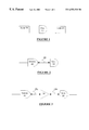
- FIG. 1 is a schematic diagram of a gate and its load
- FIG. 2 is a schematic diagram of a gate driven by an input and driving a load
- FIG. 3 is a schematic diagram of a buffered 2-pin net
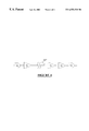
- FIG. 4 is a schematic diagram of a buffered long wire.
- ⁇ is a technology constant defined as the delay of an ideal inverter with no intrinsic delay, driving another ideal inverter.
- gate_min refers to the minimum sized gate and inv_min to the minimum sized inverter.
- h gate C load C in ( 3 )
- C load is the load capacitance 20 of the gate in the given network, and C in the input capacitance 30 .
- L is the length of the net 60
- R w and C w are the per unit length interconnect resistance and capacitance
- R so and C so are the source driver 40 resistance and input capacitance
- C si is the sink 50 input capacitance
- g so is the logical effort of the source 40
- p so is the parasitic delay of the source 40
- ⁇ is the technology constant. Note that the delay due to the source driver 40 resistance charging the sink input 50 capacitance is included in the logical effort delay and is hence omitted from the Elmore delay terms.
- D 1 ⁇ ( g so ⁇ C b + C w ⁇ L 2 C so + p so ) + R w ⁇ L 2 ⁇ ( C w ⁇ L 4 + C b ) + ⁇ ( C si + C w ⁇ L 2 C b + p b ) + R w ⁇ L 2 ⁇ ( C w ⁇ L 4 + C si ) ( 6 )
- R b and C b are the buffer driver resistance and input capacitance and p b the intrinsic delay of the buffer 70 .
- L k L/(k+1) is the distance between buffers 70 .
- buffer insertion can reduce the wire delay by dividing the delay. of one long wire segment in to two or more smaller segments.
- inserting a buffer 70 adds the buffer delay to the over-all stage delay.
- w opt be the ratio of the widths of an optimally sized buffer for a given stage and the minimum sized buffer
- k opt be the optimal number of buffers 70 for a given stage.
- k opt depends on the size of the buffer 70 being inserted since the gate delay of the buffer 70 and wire delays of the segments both depend on R b and C b .
- D k ⁇ ⁇ ⁇ ( g so ⁇ C b + C w ⁇ L k C so + p so ) + k ⁇ ⁇ ⁇ ⁇ ( 1 + C w ⁇ L k C b + p b ) + R w ⁇ C w ⁇ L k 2 + kR w ⁇ C b ⁇ L k + R w ⁇ C si ⁇ L k ( 9 )
- D k L ⁇ ( 2 ⁇ R w ⁇ C w ⁇ ⁇ ⁇ ⁇ ( 1 + p b ) + ⁇ ⁇ ⁇ C w C b ) ( 13 )
- the delay model in Equations (16) and (17). is exact for 2-pin nets 60 with an arbitrary number of equally spaced same-sized buffers 70 and with the sink 50 and source 40 sized to be the same as the buffer 70 input capacitance and driving resistance. Further, the delay model in Equations (16) and (17) is continuous and differentiable everywhere in L for 2-pin nets 60 with an arbitrary number of equally spaced same-sized buffers 70 and with the sink 50 and source 40 sized to be the same as the buffer 70 input capacitance and driving resistance. This can be seen as follows.
- D k is clearly continuous and differentiable everywhere in L except at L kopt .
- L L kopt
- lim L ⁇ L kopt - ⁇ ⁇ D k ⁇ ⁇ ( g so ⁇ ⁇ C b + C w ⁇ L C so + p so ) + R w ⁇ C w ⁇ L 2 2 + R w ⁇ C si ⁇ L ⁇ ⁇ ⁇
- R b R so
- C b C si
- g so 1 ( 18 )
- D k is both continuous and differentiable everywhere in L. Even when R b ⁇ R so , C b ⁇ C si , or g so ⁇ 1, similar results can be derived under the assumption that the 2-pin net 60 is infinitely long.
- D k ⁇ ⁇ ( g so ⁇ ⁇ C b + C w ⁇ L k C so + p so ) + k ⁇ ⁇ ⁇ ⁇ ( 1 + C k ⁇ L k C b + p b ) + R w ⁇ C w ⁇ LL k 2 + R w ⁇ C b ⁇ L k + R w ⁇ C si ⁇ L k ( 21 )
- the delay model proposed earlier can hence also be applied to nets with arbitrary sink and source under the restriction of infinite length.
- Equations 16 and 17 are exact for 2-pin nets 60 with the source 40 and sink 50 connected by an infinitely long wire 60 with an arbitrary number of equally spaced same-sized buffers 60 .
- the estimated delay approaches the exact delay as the length approaches infinity.
- the delay model in Equations 16 and 17 is continuous and differentiable everywhere in L for 2-pin nets with the source 40 and sink 50 connected by an infinitely long wire 60 with an arbitrary number of equally spaced same-sized buffers 70 .
- the above can also be demonstrated using the traditional linear delay model (which models the delay through a gate as a linear function of its load) in conjunction with the Elmore delay model.
- the delay model proposed in Equations (16) and (17) allows accurate prediction of wire delays in presence of long wires 60 .
- the delay estimates account for the effect of buffering on the delay.
- the model is exact under some assumptions and is a good heuristic approximation for the more general cases.
- the delay model framework also provides results on the optimal buffering scheme for such wires 60 . This enables a placement-optimization flow where the initial placement of cells can be performed without actually buffering long wires 60 .
- a timing-driven placement program can account for the wire delays without actually buffering long wires 60 (via the predictive delay formula) and an area/capacitance-driven placement program can account for capacitance shielding due to long wires 60 (via the optimal buffering distance formula).
- the delay of long wires 60 is a function of their length and the per unit length wire resistance.
- the resistance and capacitance per unit length of a minimum width/spacing wire be r w and c w respectively.
- the area and lateral capacitance per unit length be c a and c l (for typical deep sub-micron technologies, c a ⁇ c l ).
- D L ⁇ r w ⁇ c a + r w ⁇ c l w w ⁇ s w ⁇ ( 2 ⁇ ⁇ ⁇ ( 1 + p b ) + 2 ⁇ C 0 ⁇ ⁇ ) ( 33 )
- D k L w w ⁇ s w ⁇ ( 2 ⁇ ⁇ ⁇ ( 1 + p b ) ⁇ r w ⁇ c l + 2 ⁇ C 0 ⁇ ⁇ ⁇ r w ⁇ c l ) ( 34 )
- the wire delay can be held constant in presence of a 100% increase in wire length by doubling the width and the spacing of the wire. This observation can be used to predict and control the wire delay over a wide range of lengths during a placement-optimization flow.
- wire delay can be held constant in presence of length changes by changing the width and spacing of the wire. This can be used to assign wire sizes and widths and to compute delay budgets as follows: given a placement, the lengths of all wires are fixed. At this point, the wire delays are computed first using the wire length from the placement, minimum width and spacing and the library RC data. Given the cell delays and the computed wire delays, critical paths are identified. Wires on critical paths are than sized up/spaced out to reduce their delay and to bring the overall design slack to zero—this could be done by a simulated annealing algorithm as described in, e.g., Kirkpatrick et. al, “Optimization by Simulated Annealing,” Science, vol. 220, no. 4598, pp. 671-680, 1983, or some greedy assignment algorithm which sizes up wires with significant delays.
- the maximum allowable wire widths/sizes may be limited by technology or manufacturing constraints. Given these size and spacing assignments, wire delays are computed and stored as budgets. These delays are held constant through the flow. Subsequent wire sizings and spacings can be done on each wire individually to continue to meet these budgets in spite of any length changes (due to placement changes) and as more information like neighborhood information (during routing) is made available.
- Wire delay and capacitance estimates based on placement information can be significantly different from statistical wireload models.
- placement information e.g. Manhattan distance between pins
- the gate and wire delays can change significantly once placement is performed. This may change the arrival and requires times of signals in the circuit and a netlist optimized with wireload models may no longer be the optimal netlist when placement based wire models are applied.
- This provides a potential of re-optimizing the circuit by selectively resynthesizing parts of the network. While there are many resynthesis techniques known in the literature and resynthesis can be applied at any time, the main problem with a generic application of resynthesis is that the placement is invalidated.
- the placement technique is performed as disclosed in the United States Patent Application to Savoj et al. filed on Apr. 27, 1999, U.S. patent application Ser. No. 09/300,666 incorporated herein by reference.
- the buffering, placement, wire sizing and spacing steps can be iterated.
- this iteration includes iteration of assigned delays to account for timing changes due to the other optimization steps.
- the constant wire delay methodology does not perform iterations, in general one or more steps between updating timing and routing wires can be iterated. While more iterations may not always yield a better design and in fact may lead to convergence problems, one can come up with heuristic criteria for convergence to decide when to stop iterating.
- a crosstalk-sensitive routing program can vary size and spacing as neighboring wiring information becomes available to continue to meet the delay budgets set in the assign wire delays.
Abstract
Description


Claims (7)


Priority Applications (4)
| Application Number | Priority Date | Filing Date | Title |
|---|---|---|---|
| US09/300,557 US6553338B1 (en) | 1999-04-27 | 1999-04-27 | Timing optimization in presence of interconnect delays |
| PCT/US2000/011002 WO2000065490A1 (en) | 1999-04-27 | 2000-04-24 | Timing optimization in presence of interconnect delays |
| AU46598/00A AU4659800A (en) | 1999-04-27 | 2000-04-24 | Timing optimization in presence of interconnect delays |
| TW089107892A TW465185B (en) | 1999-04-27 | 2000-05-04 | Timing optimization in presence of interconnect delays |
Applications Claiming Priority (1)
| Application Number | Priority Date | Filing Date | Title |
|---|---|---|---|
| US09/300,557 US6553338B1 (en) | 1999-04-27 | 1999-04-27 | Timing optimization in presence of interconnect delays |
Publications (1)
| Publication Number | Publication Date |
|---|---|
| US6553338B1 true US6553338B1 (en) | 2003-04-22 |
Family
ID=23159597
Family Applications (1)
| Application Number | Title | Priority Date | Filing Date |
|---|---|---|---|
| US09/300,557 Expired - Lifetime US6553338B1 (en) | 1999-04-27 | 1999-04-27 | Timing optimization in presence of interconnect delays |
Country Status (4)
| Country | Link |
|---|---|
| US (1) | US6553338B1 (en) |
| AU (1) | AU4659800A (en) |
| TW (1) | TW465185B (en) |
| WO (1) | WO2000065490A1 (en) |
Cited By (31)
| Publication number | Priority date | Publication date | Assignee | Title |
|---|---|---|---|---|
| US20020169588A1 (en) * | 2001-05-11 | 2002-11-14 | International Business Machines Corporation | Bidirectional wire I/O model and method for device simulation |
| US20030023327A1 (en) * | 2001-07-27 | 2003-01-30 | Norman Chang | Optimization of clock scheduling for a synchronous system |
| US20030182648A1 (en) * | 2002-03-20 | 2003-09-25 | Fujitsu Limited | Method, apparatus and program product for automatic placement and routing of integrated circuit |
| US6701506B1 (en) * | 2001-12-14 | 2004-03-02 | Sequence Design, Inc. | Method for match delay buffer insertion |
| US20040078770A1 (en) * | 1999-10-14 | 2004-04-22 | Synopsys, Inc. | Detailed placer for optimizing high density cell placement in a linear runtime |
| US20040243953A1 (en) * | 2003-05-30 | 2004-12-02 | Champaka Ramachandran | Method and apparatus for automated circuit design |
| US20040243964A1 (en) * | 2003-05-30 | 2004-12-02 | Mcelvain Kenneth S. | Method and apparatus for automated circuit design |
| US20050064347A1 (en) * | 2003-09-24 | 2005-03-24 | Yao-Ting Wang | Frequency division multiplexing (FDM) lithography |
| US20050108666A1 (en) * | 2003-11-06 | 2005-05-19 | Li-Fu Chang | Delta information design closure in integrated circuit fabrication |
| US20050155007A1 (en) * | 2004-01-09 | 2005-07-14 | Matsushita Electric Industrial Co., Ltd. | Automatic layout method of semiconductor integrated circuit |
| US20050172251A1 (en) * | 2003-11-06 | 2005-08-04 | Li-Fu Chang | Delta-geometry timing prediction in integrated circuit fabrication |
| US20050210434A1 (en) * | 2004-01-09 | 2005-09-22 | Airbus France | Process for the production of an electrical wiring diagram |
| US20060193329A1 (en) * | 2005-02-28 | 2006-08-31 | Rajiv Asati | Method and apparatus for limiting VPNv4 prefixes per VPN in an inter-autonomous system environment |
| US20060242618A1 (en) * | 2005-02-14 | 2006-10-26 | Yao-Ting Wang | Lithographic simulations using graphical processing units |
| WO2007035681A1 (en) * | 2005-09-16 | 2007-03-29 | Qualcomm Incorporated | Exploration of the method of the interconnect effort in nano-technologies |
| US20070094623A1 (en) * | 2005-10-24 | 2007-04-26 | Haizhou Chen | Timing, noise, and power analysis of integrated circuits |
| US7257797B1 (en) * | 2004-06-07 | 2007-08-14 | Pulsic Limited | Method of automatic shape-based routing of interconnects in spines for integrated circuit design |
| US7260804B1 (en) | 2004-09-21 | 2007-08-21 | Golden Gate Technology, Inc. | Method for circuit block routing based on switching activity |
| US7360193B1 (en) | 2004-09-21 | 2008-04-15 | Golden Gate Technology, Inc. | Method for circuit block placement and circuit block arrangement based on switching activity |
| US20080302172A1 (en) * | 2004-09-23 | 2008-12-11 | Lawrence Kates | System and method for utility metering and leak detection |
| US20080320428A1 (en) * | 2007-06-22 | 2008-12-25 | Synopsys, Inc. | Minimizing Effects of Interconnect Variations in Integrated Circuit Designs |
| US20090235217A1 (en) * | 2008-03-11 | 2009-09-17 | International Business Machines Corporation | Method to identify timing violations outside of manufacturing specification limits |
| US20100049481A1 (en) * | 2008-08-25 | 2010-02-25 | Fujitsu Limited | Constructing a Replica-Based Clock Tree |
| US7823112B1 (en) | 2003-05-30 | 2010-10-26 | Golden Gate Technology, Inc. | Method, software and system for ensuring timing between clocked components in a circuit |
| US7992122B1 (en) | 2005-03-25 | 2011-08-02 | Gg Technology, Inc. | Method of placing and routing for power optimization and timing closure |
| US8015533B1 (en) | 2004-09-21 | 2011-09-06 | Golden Gate Technology, Inc. | Method for matching timing on high fanout signal paths using routing guides |
| US8453090B2 (en) | 2010-10-21 | 2013-05-28 | Global Unichip Corp. | System and method for optimizing logic timing |
| US8458636B1 (en) | 2009-03-18 | 2013-06-04 | Pulsic Limited | Filling vacant areas of an integrated circuit design |
| US20160056800A1 (en) * | 2014-08-25 | 2016-02-25 | Samsung Electronics Co., Ltd. | Semiconductor device having driver structure for reducing circuit area |
| US10216890B2 (en) | 2004-04-21 | 2019-02-26 | Iym Technologies Llc | Integrated circuits having in-situ constraints |
| US10839120B2 (en) | 2018-02-21 | 2020-11-17 | Sharif University Of Technology | Communication at the speed of light over an on-chip interconnect |
Families Citing this family (1)
| Publication number | Priority date | Publication date | Assignee | Title |
|---|---|---|---|---|
| US7010767B2 (en) * | 2000-11-01 | 2006-03-07 | Cadence Design Systems, Inc. | Insertion of repeaters without timing constraints |
Citations (4)
| Publication number | Priority date | Publication date | Assignee | Title |
|---|---|---|---|---|
| US5838580A (en) | 1996-06-20 | 1998-11-17 | Sun Microsystems, Inc. | Method of optimizing repeater placement in long lines of a complex integrated circuit |
| US6002268A (en) * | 1993-01-08 | 1999-12-14 | Dynachip Corporation | FPGA with conductors segmented by active repeaters |
| US6009253A (en) * | 1996-06-20 | 1999-12-28 | Sun Microsystems, Inc. | Spare repeater amplifiers for long lines on complex integrated circuits |
| US6117182A (en) * | 1998-06-12 | 2000-09-12 | International Business Machines Corporation | Optimum buffer placement for noise avoidance |
-
1999
- 1999-04-27 US US09/300,557 patent/US6553338B1/en not_active Expired - Lifetime
-
2000
- 2000-04-24 WO PCT/US2000/011002 patent/WO2000065490A1/en active Application Filing
- 2000-04-24 AU AU46598/00A patent/AU4659800A/en not_active Abandoned
- 2000-05-04 TW TW089107892A patent/TW465185B/en not_active IP Right Cessation
Patent Citations (4)
| Publication number | Priority date | Publication date | Assignee | Title |
|---|---|---|---|---|
| US6002268A (en) * | 1993-01-08 | 1999-12-14 | Dynachip Corporation | FPGA with conductors segmented by active repeaters |
| US5838580A (en) | 1996-06-20 | 1998-11-17 | Sun Microsystems, Inc. | Method of optimizing repeater placement in long lines of a complex integrated circuit |
| US6009253A (en) * | 1996-06-20 | 1999-12-28 | Sun Microsystems, Inc. | Spare repeater amplifiers for long lines on complex integrated circuits |
| US6117182A (en) * | 1998-06-12 | 2000-09-12 | International Business Machines Corporation | Optimum buffer placement for noise avoidance |
Non-Patent Citations (5)
| Title |
|---|
| Alpert et al., "Wire segmenting for improved buffer insertion", Design automation Confeerence, Jun. 1997.* * |
| Dhar, S.; Franklin, M.A.; "Optimum Buffer Circuits for Driving Long Uniform Lines," IEEE Journal of Solid-State Circuits, 1/91, vol. 26, No. 1, pp. 32-40. |
| Nekili, M.; Savaria, Y., "Optimal Methods of Driving Interconnections in VLSI Circuits," 1992 IEEE Intl Symposium on Circuits and Systems, San Diego, CA, May 10-13 1992, pp. 21-24. |
| Pullela et al. "Post processing of clock trees via wiresizing and buffering for robust design", IEEE transactions on Computer aided design of Integrated circuits and systems Jun. 1996.* * |
| Venkat, K., "Generalized Delay Optimization of Resistive Interconnections through an Extension of Logic Effort," (Proc.) 1993 IEEE Intl Symposium on Circuits and Systems, Chicago, IL, 306 May 1993; pp. 2106-2109. |
Cited By (74)
| Publication number | Priority date | Publication date | Assignee | Title |
|---|---|---|---|---|
| US8069429B2 (en) | 1999-10-14 | 2011-11-29 | Synopsys, Inc. | Detailed placer for optimizing high density cell placement in a linear runtime |
| US20080250375A1 (en) * | 1999-10-14 | 2008-10-09 | Synopsys, Inc. | Detailed Placer For Optimizing High Density Cell Placement In A Linear Runtime |
| US20040078770A1 (en) * | 1999-10-14 | 2004-04-22 | Synopsys, Inc. | Detailed placer for optimizing high density cell placement in a linear runtime |
| US7404168B2 (en) | 1999-10-14 | 2008-07-22 | Synopsys, Inc. | Detailed placer for optimizing high density cell placement in a linear runtime |
| US20060090151A1 (en) * | 1999-10-14 | 2006-04-27 | Synopsys, Inc. | Detailed placer for optimizing high density cell placement in a linear runtime |
| US7036103B2 (en) * | 1999-10-14 | 2006-04-25 | Synopsys, Inc. | Detailed placer for optimizing high density cell placement in a linear runtime |
| US6985842B2 (en) * | 2001-05-11 | 2006-01-10 | International Business Machines Corporation | Bidirectional wire I/O model and method for device simulation |
| US20020169588A1 (en) * | 2001-05-11 | 2002-11-14 | International Business Machines Corporation | Bidirectional wire I/O model and method for device simulation |
| US6925555B2 (en) * | 2001-07-27 | 2005-08-02 | Hewlett-Packard Development Company, L.P. | System and method for determining a plurality of clock delay values using an optimization algorithm |
| US20030023327A1 (en) * | 2001-07-27 | 2003-01-30 | Norman Chang | Optimization of clock scheduling for a synchronous system |
| US6701506B1 (en) * | 2001-12-14 | 2004-03-02 | Sequence Design, Inc. | Method for match delay buffer insertion |
| US6968521B2 (en) * | 2002-03-20 | 2005-11-22 | Fujitsu Limited | Method, apparatus and program product for automatic placement and routing of integrated circuit |
| US20030182648A1 (en) * | 2002-03-20 | 2003-09-25 | Fujitsu Limited | Method, apparatus and program product for automatic placement and routing of integrated circuit |
| US20040243953A1 (en) * | 2003-05-30 | 2004-12-02 | Champaka Ramachandran | Method and apparatus for automated circuit design |
| US8990743B2 (en) | 2003-05-30 | 2015-03-24 | Synopsys, Inc. | Automated circuit design |
| US8151228B2 (en) | 2003-05-30 | 2012-04-03 | Synopsys, Inc. | Method and apparatus for automated circuit design |
| WO2004109562A1 (en) * | 2003-05-30 | 2004-12-16 | Sinplicity, Inc. | Method and apparatus for automated circuit design |
| US20040243964A1 (en) * | 2003-05-30 | 2004-12-02 | Mcelvain Kenneth S. | Method and apparatus for automated circuit design |
| US7823112B1 (en) | 2003-05-30 | 2010-10-26 | Golden Gate Technology, Inc. | Method, software and system for ensuring timing between clocked components in a circuit |
| US7251800B2 (en) | 2003-05-30 | 2007-07-31 | Synplicity, Inc. | Method and apparatus for automated circuit design |
| US7178118B2 (en) | 2003-05-30 | 2007-02-13 | Synplicity, Inc. | Method and apparatus for automated circuit design |
| US8661375B2 (en) | 2003-09-24 | 2014-02-25 | Cadence Design Systems, Inc. | Frequency division multiplexing (FDM) lithography |
| US20110154274A1 (en) * | 2003-09-24 | 2011-06-23 | Yao-Ting Wang | Frequency division multiplexing (fdm) lithography |
| US7879538B2 (en) | 2003-09-24 | 2011-02-01 | Cadence Design Systems, Inc. | Frequency division multiplexing (FDM) lithography |
| US20050064347A1 (en) * | 2003-09-24 | 2005-03-24 | Yao-Ting Wang | Frequency division multiplexing (FDM) lithography |
| US20050108666A1 (en) * | 2003-11-06 | 2005-05-19 | Li-Fu Chang | Delta information design closure in integrated circuit fabrication |
| US7216320B2 (en) * | 2003-11-06 | 2007-05-08 | Clear Shape Technologies, Inc. | Delta-geometry timing prediction in integrated circuit fabrication |
| US20050172251A1 (en) * | 2003-11-06 | 2005-08-04 | Li-Fu Chang | Delta-geometry timing prediction in integrated circuit fabrication |
| US7360191B2 (en) | 2003-11-06 | 2008-04-15 | Clear Shape Technologies, Inc. | Delta information design closure integrated circuit fabrication |
| US20050210434A1 (en) * | 2004-01-09 | 2005-09-22 | Airbus France | Process for the production of an electrical wiring diagram |
| US20050155007A1 (en) * | 2004-01-09 | 2005-07-14 | Matsushita Electric Industrial Co., Ltd. | Automatic layout method of semiconductor integrated circuit |
| US7272811B2 (en) * | 2004-01-09 | 2007-09-18 | Matsushita Electric Industrial Co., Ltd. | Automatic layout method of semiconductor integrated circuit |
| US7409663B2 (en) * | 2004-01-09 | 2008-08-05 | Airbus France | Process for the production of an electrical wiring diagram |
| US10216890B2 (en) | 2004-04-21 | 2019-02-26 | Iym Technologies Llc | Integrated circuits having in-situ constraints |
| US10846454B2 (en) | 2004-04-21 | 2020-11-24 | Iym Technologies Llc | Integrated circuits having in-situ constraints |
| US10860773B2 (en) | 2004-04-21 | 2020-12-08 | Iym Technologies Llc | Integrated circuits having in-situ constraints |
| US7802208B1 (en) | 2004-06-07 | 2010-09-21 | Pulsic Limited | Design automation using spine routing |
| US8099700B1 (en) | 2004-06-07 | 2012-01-17 | Pulsic Limited | Automatic integrated circuit routing using spines |
| US7257797B1 (en) * | 2004-06-07 | 2007-08-14 | Pulsic Limited | Method of automatic shape-based routing of interconnects in spines for integrated circuit design |
| US8479141B1 (en) | 2004-06-07 | 2013-07-02 | Pulsic Limited | Automation using spine routing |
| US7823113B1 (en) | 2004-06-07 | 2010-10-26 | Pulsic Limited | Automatic integrated circuit routing using spines |
| US7360193B1 (en) | 2004-09-21 | 2008-04-15 | Golden Gate Technology, Inc. | Method for circuit block placement and circuit block arrangement based on switching activity |
| US7260804B1 (en) | 2004-09-21 | 2007-08-21 | Golden Gate Technology, Inc. | Method for circuit block routing based on switching activity |
| US8015533B1 (en) | 2004-09-21 | 2011-09-06 | Golden Gate Technology, Inc. | Method for matching timing on high fanout signal paths using routing guides |
| US20080302172A1 (en) * | 2004-09-23 | 2008-12-11 | Lawrence Kates | System and method for utility metering and leak detection |
| US20060242618A1 (en) * | 2005-02-14 | 2006-10-26 | Yao-Ting Wang | Lithographic simulations using graphical processing units |
| US20060193329A1 (en) * | 2005-02-28 | 2006-08-31 | Rajiv Asati | Method and apparatus for limiting VPNv4 prefixes per VPN in an inter-autonomous system environment |
| US7385988B2 (en) | 2005-02-28 | 2008-06-10 | Cisco Technology, Inc. | Method and apparatus for limiting VPNv4 prefixes per VPN in an inter-autonomous system environment |
| US7992122B1 (en) | 2005-03-25 | 2011-08-02 | Gg Technology, Inc. | Method of placing and routing for power optimization and timing closure |
| JP2009509249A (en) * | 2005-09-16 | 2009-03-05 | クゥアルコム・インコーポレイテッド | Exploring methods of interconnect effort in nanotechnology |
| US20070136706A1 (en) * | 2005-09-16 | 2007-06-14 | Qualcomm Incorporated | Exploration Of The Method Of The Interconnect Effort In Nano-Technologies |
| WO2007035681A1 (en) * | 2005-09-16 | 2007-03-29 | Qualcomm Incorporated | Exploration of the method of the interconnect effort in nano-technologies |
| US7721236B2 (en) * | 2005-09-16 | 2010-05-18 | Qualcomm Incorporated | Method and apparatus of estimating circuit delay |
| CN101305372B (en) * | 2005-09-16 | 2010-05-26 | 高通股份有限公司 | Estimation circuit delay method and device |
| US8225248B2 (en) | 2005-10-24 | 2012-07-17 | Cadence Design Systems, Inc. | Timing, noise, and power analysis of integrated circuits |
| US7673260B2 (en) | 2005-10-24 | 2010-03-02 | Cadence Design Systems, Inc. | Modeling device variations in integrated circuit design |
| US20070094623A1 (en) * | 2005-10-24 | 2007-04-26 | Haizhou Chen | Timing, noise, and power analysis of integrated circuits |
| US20070099314A1 (en) * | 2005-10-24 | 2007-05-03 | Haizhou Chen | Modeling device variations in integrated circuit design |
| US20080320428A1 (en) * | 2007-06-22 | 2008-12-25 | Synopsys, Inc. | Minimizing Effects of Interconnect Variations in Integrated Circuit Designs |
| US20090319960A1 (en) * | 2007-06-22 | 2009-12-24 | Synopsys, Inc. | Minimizing Effects of Interconnect Variations in Integrated Circuit Designs |
| US7908573B2 (en) | 2007-06-22 | 2011-03-15 | Synopsys, Inc. | Minimizing effects of interconnect variations in integrated circuit designs |
| US7669161B2 (en) | 2007-06-22 | 2010-02-23 | Synopsys, Inc. | Minimizing effects of interconnect variations in integrated circuit designs |
| US20090235217A1 (en) * | 2008-03-11 | 2009-09-17 | International Business Machines Corporation | Method to identify timing violations outside of manufacturing specification limits |
| US7844932B2 (en) | 2008-03-11 | 2010-11-30 | International Business Machines Corporation | Method to identify timing violations outside of manufacturing specification limits |
| US8255196B2 (en) * | 2008-08-25 | 2012-08-28 | Fujitsu Limited | Constructing a replica-based clock tree |
| US20100049481A1 (en) * | 2008-08-25 | 2010-02-25 | Fujitsu Limited | Constructing a Replica-Based Clock Tree |
| US9767242B1 (en) | 2009-03-18 | 2017-09-19 | Pulsic Limited | Filling vacant areas of an integrated circuit design |
| US8458636B1 (en) | 2009-03-18 | 2013-06-04 | Pulsic Limited | Filling vacant areas of an integrated circuit design |
| US10691858B1 (en) | 2009-03-18 | 2020-06-23 | Pulsic Limited | Filing vacant areas of an integrated circuit design |
| US11030374B1 (en) | 2009-03-18 | 2021-06-08 | Pulsic Limited | Filling vacant areas of an integrated circuit design |
| US11853671B1 (en) | 2009-03-18 | 2023-12-26 | Pulsic Limited | Filling vacant areas of an integrated circuit design |
| US8453090B2 (en) | 2010-10-21 | 2013-05-28 | Global Unichip Corp. | System and method for optimizing logic timing |
| US20160056800A1 (en) * | 2014-08-25 | 2016-02-25 | Samsung Electronics Co., Ltd. | Semiconductor device having driver structure for reducing circuit area |
| US10839120B2 (en) | 2018-02-21 | 2020-11-17 | Sharif University Of Technology | Communication at the speed of light over an on-chip interconnect |
Also Published As
| Publication number | Publication date |
|---|---|
| AU4659800A (en) | 2000-11-10 |
| WO2000065490A1 (en) | 2000-11-02 |
| TW465185B (en) | 2001-11-21 |
Similar Documents
| Publication | Publication Date | Title |
|---|---|---|
| US6553338B1 (en) | Timing optimization in presence of interconnect delays | |
| US6496965B1 (en) | Automated design of parallel drive standard cells | |
| US7251800B2 (en) | Method and apparatus for automated circuit design | |
| US6725438B2 (en) | Timing closure methodology | |
| US7178118B2 (en) | Method and apparatus for automated circuit design | |
| US6080201A (en) | Integrated placement and synthesis for timing closure of microprocessors | |
| US7676780B2 (en) | Techniques for super fast buffer insertion | |
| US7890905B2 (en) | Slew constrained minimum cost buffering | |
| US20100122227A1 (en) | System and Technique of Pattern Matching and Pattern Replacement | |
| Cong et al. | Interconnect delay estimation models for synthesis and design planning | |
| US6397169B1 (en) | Adaptive cell separation and circuit changes driven by maximum capacitance rules | |
| US6192508B1 (en) | Method for logic optimization for improving timing and congestion during placement in integrated circuit design | |
| Papa et al. | RUMBLE: an incremental, timing-driven, physical-synthesis optimization algorithm | |
| US7100140B2 (en) | Generation of graphical congestion data during placement driven synthesis optimization | |
| US20090125859A1 (en) | Methods for Optimal Timing-Driven Cloning Under Linear Delay Model | |
| JP2004102703A (en) | Design support device for register transfer level | |
| US6931610B1 (en) | Method for rapid estimation of wire delays and capacitances based on placement of cells | |
| Ababei et al. | Timing minimization by statistical timing hMetis-Based partitioning | |
| CN116341479A (en) | Remapping method based on routability and integrated circuit | |
| Sulimma et al. | Improving placement under the constant delay model | |
| Beraudo | A path based algorithm for timing driven logic replication in FPGA | |
| Alpert et al. | Placement-Driven Synthesis Design Closure Tool |
Legal Events
| Date | Code | Title | Description |
|---|---|---|---|
| AS | Assignment |
Owner name: MAGMA DESIGN AUTOMATION, INC., CALIFORNIA Free format text: ASSIGNMENT OF ASSIGNORS INTEREST;ASSIGNORS:BUCH, PREMAL V.;SAVOJ, HAMID;VAN GINNEKEN, LUKAS P.P.P.;REEL/FRAME:010114/0896;SIGNING DATES FROM 19990628 TO 19990630 |
|
| STCF | Information on status: patent grant |
Free format text: PATENTED CASE |
|
| FEPP | Fee payment procedure |
Free format text: PAT HOLDER NO LONGER CLAIMS SMALL ENTITY STATUS, ENTITY STATUS SET TO UNDISCOUNTED (ORIGINAL EVENT CODE: STOL); ENTITY STATUS OF PATENT OWNER: LARGE ENTITY |
|
| FPAY | Fee payment |
Year of fee payment: 4 |
|
| AS | Assignment |
Owner name: WELLS FARGO CAPITAL FINANCE, LLC,CALIFORNIA Free format text: SECURITY AGREEMENT;ASSIGNOR:MAGMA DESIGN AUTOMATION, INC.;REEL/FRAME:024120/0809 Effective date: 20100319 Owner name: WELLS FARGO CAPITAL FINANCE, LLC, CALIFORNIA Free format text: SECURITY AGREEMENT;ASSIGNOR:MAGMA DESIGN AUTOMATION, INC.;REEL/FRAME:024120/0809 Effective date: 20100319 |
|
| FPAY | Fee payment |
Year of fee payment: 8 |
|
| FPAY | Fee payment |
Year of fee payment: 12 |
|
| AS | Assignment |
Owner name: SYNOPSYS, INC., CALIFORNIA Free format text: RELEASE BY SECURED PARTY;ASSIGNOR:WELLS FARGO CAPITAL FINANCE, LLC;REEL/FRAME:040607/0632 Effective date: 20161031 |