US6555924B2 - Semiconductor package with flash preventing mechanism and fabrication method thereof - Google Patents
Semiconductor package with flash preventing mechanism and fabrication method thereof Download PDFInfo
- Publication number
- US6555924B2 US6555924B2 US09/932,054 US93205401A US6555924B2 US 6555924 B2 US6555924 B2 US 6555924B2 US 93205401 A US93205401 A US 93205401A US 6555924 B2 US6555924 B2 US 6555924B2
- Authority
- US
- United States
- Prior art keywords
- semiconductor package
- substrate
- preventing mechanism
- molding compound
- flash
- Prior art date
- Legal status (The legal status is an assumption and is not a legal conclusion. Google has not performed a legal analysis and makes no representation as to the accuracy of the status listed.)
- Expired - Lifetime
Links
Images


Classifications
-
- B—PERFORMING OPERATIONS; TRANSPORTING
- B29—WORKING OF PLASTICS; WORKING OF SUBSTANCES IN A PLASTIC STATE IN GENERAL
- B29C—SHAPING OR JOINING OF PLASTICS; SHAPING OF MATERIAL IN A PLASTIC STATE, NOT OTHERWISE PROVIDED FOR; AFTER-TREATMENT OF THE SHAPED PRODUCTS, e.g. REPAIRING
- B29C45/00—Injection moulding, i.e. forcing the required volume of moulding material through a nozzle into a closed mould; Apparatus therefor
- B29C45/17—Component parts, details or accessories; Auxiliary operations
- B29C45/26—Moulds
- B29C45/34—Moulds having venting means
-
- H—ELECTRICITY
- H01—ELECTRIC ELEMENTS
- H01L—SEMICONDUCTOR DEVICES NOT COVERED BY CLASS H10
- H01L21/00—Processes or apparatus adapted for the manufacture or treatment of semiconductor or solid state devices or of parts thereof
- H01L21/02—Manufacture or treatment of semiconductor devices or of parts thereof
- H01L21/04—Manufacture or treatment of semiconductor devices or of parts thereof the devices having at least one potential-jump barrier or surface barrier, e.g. PN junction, depletion layer or carrier concentration layer
- H01L21/50—Assembly of semiconductor devices using processes or apparatus not provided for in a single one of the subgroups H01L21/06 - H01L21/326, e.g. sealing of a cap to a base of a container
- H01L21/56—Encapsulations, e.g. encapsulation layers, coatings
- H01L21/565—Moulds
-
- H—ELECTRICITY
- H01—ELECTRIC ELEMENTS
- H01L—SEMICONDUCTOR DEVICES NOT COVERED BY CLASS H10
- H01L23/00—Details of semiconductor or other solid state devices
- H01L23/564—Details not otherwise provided for, e.g. protection against moisture
-
- H—ELECTRICITY
- H01—ELECTRIC ELEMENTS
- H01L—SEMICONDUCTOR DEVICES NOT COVERED BY CLASS H10
- H01L2224/00—Indexing scheme for arrangements for connecting or disconnecting semiconductor or solid-state bodies and methods related thereto as covered by H01L24/00
- H01L2224/01—Means for bonding being attached to, or being formed on, the surface to be connected, e.g. chip-to-package, die-attach, "first-level" interconnects; Manufacturing methods related thereto
- H01L2224/10—Bump connectors; Manufacturing methods related thereto
- H01L2224/15—Structure, shape, material or disposition of the bump connectors after the connecting process
- H01L2224/16—Structure, shape, material or disposition of the bump connectors after the connecting process of an individual bump connector
- H01L2224/161—Disposition
- H01L2224/16151—Disposition the bump connector connecting between a semiconductor or solid-state body and an item not being a semiconductor or solid-state body, e.g. chip-to-substrate, chip-to-passive
- H01L2224/16221—Disposition the bump connector connecting between a semiconductor or solid-state body and an item not being a semiconductor or solid-state body, e.g. chip-to-substrate, chip-to-passive the body and the item being stacked
- H01L2224/16225—Disposition the bump connector connecting between a semiconductor or solid-state body and an item not being a semiconductor or solid-state body, e.g. chip-to-substrate, chip-to-passive the body and the item being stacked the item being non-metallic, e.g. insulating substrate with or without metallisation
-
- H—ELECTRICITY
- H01—ELECTRIC ELEMENTS
- H01L—SEMICONDUCTOR DEVICES NOT COVERED BY CLASS H10
- H01L2224/00—Indexing scheme for arrangements for connecting or disconnecting semiconductor or solid-state bodies and methods related thereto as covered by H01L24/00
- H01L2224/01—Means for bonding being attached to, or being formed on, the surface to be connected, e.g. chip-to-package, die-attach, "first-level" interconnects; Manufacturing methods related thereto
- H01L2224/26—Layer connectors, e.g. plate connectors, solder or adhesive layers; Manufacturing methods related thereto
- H01L2224/31—Structure, shape, material or disposition of the layer connectors after the connecting process
- H01L2224/32—Structure, shape, material or disposition of the layer connectors after the connecting process of an individual layer connector
- H01L2224/321—Disposition
- H01L2224/32151—Disposition the layer connector connecting between a semiconductor or solid-state body and an item not being a semiconductor or solid-state body, e.g. chip-to-substrate, chip-to-passive
- H01L2224/32221—Disposition the layer connector connecting between a semiconductor or solid-state body and an item not being a semiconductor or solid-state body, e.g. chip-to-substrate, chip-to-passive the body and the item being stacked
- H01L2224/32225—Disposition the layer connector connecting between a semiconductor or solid-state body and an item not being a semiconductor or solid-state body, e.g. chip-to-substrate, chip-to-passive the body and the item being stacked the item being non-metallic, e.g. insulating substrate with or without metallisation
-
- H—ELECTRICITY
- H01—ELECTRIC ELEMENTS
- H01L—SEMICONDUCTOR DEVICES NOT COVERED BY CLASS H10
- H01L2224/00—Indexing scheme for arrangements for connecting or disconnecting semiconductor or solid-state bodies and methods related thereto as covered by H01L24/00
- H01L2224/01—Means for bonding being attached to, or being formed on, the surface to be connected, e.g. chip-to-package, die-attach, "first-level" interconnects; Manufacturing methods related thereto
- H01L2224/42—Wire connectors; Manufacturing methods related thereto
- H01L2224/47—Structure, shape, material or disposition of the wire connectors after the connecting process
- H01L2224/48—Structure, shape, material or disposition of the wire connectors after the connecting process of an individual wire connector
- H01L2224/481—Disposition
- H01L2224/48151—Connecting between a semiconductor or solid-state body and an item not being a semiconductor or solid-state body, e.g. chip-to-substrate, chip-to-passive
- H01L2224/48221—Connecting between a semiconductor or solid-state body and an item not being a semiconductor or solid-state body, e.g. chip-to-substrate, chip-to-passive the body and the item being stacked
- H01L2224/48225—Connecting between a semiconductor or solid-state body and an item not being a semiconductor or solid-state body, e.g. chip-to-substrate, chip-to-passive the body and the item being stacked the item being non-metallic, e.g. insulating substrate with or without metallisation
- H01L2224/48227—Connecting between a semiconductor or solid-state body and an item not being a semiconductor or solid-state body, e.g. chip-to-substrate, chip-to-passive the body and the item being stacked the item being non-metallic, e.g. insulating substrate with or without metallisation connecting the wire to a bond pad of the item
-
- H—ELECTRICITY
- H01—ELECTRIC ELEMENTS
- H01L—SEMICONDUCTOR DEVICES NOT COVERED BY CLASS H10
- H01L2224/00—Indexing scheme for arrangements for connecting or disconnecting semiconductor or solid-state bodies and methods related thereto as covered by H01L24/00
- H01L2224/73—Means for bonding being of different types provided for in two or more of groups H01L2224/10, H01L2224/18, H01L2224/26, H01L2224/34, H01L2224/42, H01L2224/50, H01L2224/63, H01L2224/71
- H01L2224/732—Location after the connecting process
- H01L2224/73251—Location after the connecting process on different surfaces
- H01L2224/73265—Layer and wire connectors
-
- H—ELECTRICITY
- H01—ELECTRIC ELEMENTS
- H01L—SEMICONDUCTOR DEVICES NOT COVERED BY CLASS H10
- H01L24/00—Arrangements for connecting or disconnecting semiconductor or solid-state bodies; Methods or apparatus related thereto
- H01L24/73—Means for bonding being of different types provided for in two or more of groups H01L24/10, H01L24/18, H01L24/26, H01L24/34, H01L24/42, H01L24/50, H01L24/63, H01L24/71
-
- H—ELECTRICITY
- H01—ELECTRIC ELEMENTS
- H01L—SEMICONDUCTOR DEVICES NOT COVERED BY CLASS H10
- H01L2924/00—Indexing scheme for arrangements or methods for connecting or disconnecting semiconductor or solid-state bodies as covered by H01L24/00
- H01L2924/10—Details of semiconductor or other solid state devices to be connected
- H01L2924/11—Device type
- H01L2924/14—Integrated circuits
-
- H—ELECTRICITY
- H01—ELECTRIC ELEMENTS
- H01L—SEMICONDUCTOR DEVICES NOT COVERED BY CLASS H10
- H01L2924/00—Indexing scheme for arrangements or methods for connecting or disconnecting semiconductor or solid-state bodies as covered by H01L24/00
- H01L2924/15—Details of package parts other than the semiconductor or other solid state devices to be connected
- H01L2924/151—Die mounting substrate
- H01L2924/153—Connection portion
- H01L2924/1531—Connection portion the connection portion being formed only on the surface of the substrate opposite to the die mounting surface
- H01L2924/15311—Connection portion the connection portion being formed only on the surface of the substrate opposite to the die mounting surface being a ball array, e.g. BGA
-
- H—ELECTRICITY
- H01—ELECTRIC ELEMENTS
- H01L—SEMICONDUCTOR DEVICES NOT COVERED BY CLASS H10
- H01L2924/00—Indexing scheme for arrangements or methods for connecting or disconnecting semiconductor or solid-state bodies as covered by H01L24/00
- H01L2924/15—Details of package parts other than the semiconductor or other solid state devices to be connected
- H01L2924/181—Encapsulation
- H01L2924/1815—Shape
Definitions
- the present invention relates to semiconductor packages and fabricating methods thereof, and more particularly, to a semiconductor package having a semiconductor chip mounted on a substrate and a fabricating method thereof
- a conventional BGA (ball grid array) semiconductor package employs an advanced technology, in which a substrate has a front side for disposing a semiconductor chip thereon and a back side for implanting a plurality of solder balls, so as to provide high density of I/O connections for electrically connecting the semiconductor package to an external printed circuit board.
- a FCBGA (flip-chip ball grid array) semiconductor package is more improved than the conventional BGA semiconductor package, in that a semiconductor chip is mounted in the FCBGA semiconductor package in an upside-down manner that the chip has an upper side downwardly reflowed to a front side of a substrate by a plurality of solder bumps, while on a back side of the substrate there are implanted a plurality of solder balls for electrically connecting the semiconductor package to an external device, and accordingly the semiconductor package can be miniaturized in profile.
- the solder bumps for mounting the chip on the substrate are disposed in a manner that a cavity is formed between the chip and the substrate. If the cavity is not filled with an insulative material, the chip and the substrate tend to be structurally damaged by a thermal stress generated from the difference in coefficient of thermal expansion (CTE) between the chip and the substrate during a temperature cycle in subsequent fabricating processes. Therefore, a flip chip underfill process, which fills the cavity between the chip and the substrate with the insulative material such as epoxy resin, is essential for fabricating the FCBGA semiconductor package, so as to enhance the structural strength for the semiconductor package.
- the insulative material such as epoxy resin
- U.S. Pat. Nos. 5,535,101 “Leadless Integrated Circuit Package” and U.S. Pat. No. 5,218,234 “Semiconductor Device with Controlled Spread Polymeric Underfill” have respectively disclosed a flip chip underfill technology; however, drawbacks have been found for the technology as follows.
- the flip chip underfill technology employs a capillary filling technique, which requires long filling time and tends to cause the formation of voids.
- an ideal material used for filling the cavity between the chip and the substrate is commonly added with a solid filler for making the filling material have a similar CTE to that of the solder bumps, so as to protect the solder bumps from being damaged by a thermal stress.
- the addition of the solid filler significantly increases a viscosity of the filling material, which makes the filling material reduced in fluidity and the filling time further prolonged.
- U.S. Pat. No. 6,038,136 discloses a simplified flip chip underfill technology, that is, a molded underfill technology in a molding process.
- a FCBGA semiconductor package 1 includes a substrate 10 having a front side 100 pre-formed with a chip bonding region 102 thereon for reflowing a semiconductor chip 12 on the chip bonding region 102 in a flip chip manner via a plurality of solder bumps 11 ; while the substrate 10 has a back side 101 to be covered by a solder mask 16 in a manner that a plurality of solder pads 18 formed on the back side 101 are exposed for implanting a plurality of solder balls (not shown) thereon, and further, a specified molding compound 19 is used for encapsulating the chip 12 and the solder bumps 11 .
- the molding compound 19 is a low viscous epoxy resin containing a solid filler in 70-90%, wherein the solid filler consists of flue particles having small particle diameters within 0.01-0.05 mm such as
- the foregoing underfill technology is characterized in that the filling for a cavity between the chip 12 and the substrate 10 is implemented in the molding process.
- a filling material 19 (same as the molding compound 19 ) is injected into a mold (not shown)
- excess air can escape through a plurality of air vents 17 connected to the outside for preventing the formation of voids.
- the filling material 19 having high fluidity and a fine filler with a particle diameter smaller than 20 ⁇ m, and the air vents 17 about 40-50 ⁇ m in height are much higher than the filler's particle diameter, the low viscous filling material 19 can therefore freely leak out of the air vents 17 , making the filling material 19 seriously flash around the air vents 17 .
- the flashing material 19 can further flow through slots 104 at two sides of the substrate 10 to a bottom surface of the semiconductor package 1 , making the mold hard to be removed from the semiconductor package 1 due to the stickiness of the flashing material 19 ; while the solder pads (not shown) formed on the back side 101 of the substrate 10 can also be easily contaminated by the flashing material 19 , and accordingly implantation of the solder balls on the solder pads is deteriorated in quality.
- a primary objective of the present invention is to provide a semiconductor package and a fabricating method thereof, in which a flash preventing mechanism is formed at a front end of an air vent, for reducing an entry space of the air vent and accordingly making a molding compound flow slowly into the air vent, so as to help prevent the molding compound from flashing on a surface of a substrate.
- flash of the molding compound can be prevented from occurring on a bottom surface of the semiconductor package in the invention, for allowing a mold to be easily removed after completing a molding process.
- the invention allows solder pads formed on the substrate to be free of flash, so as to assure the quality of an implantation process for implanting solder balls on the solder pads.
- the present invention proposes a semiconductor package and a fabricating method thereof, comprising: a substrate having a front side and a back side is prepared, wherein the front side is pre-formed with a chip bonding region, and on the front side around the chip bonding region there are disposed a plurality of flash preventing mechanisms corresponding in position to entries of air vents in a mold; a semiconductor chip is mounted on the chip bonding region and electrically connected to the substrate; and an encapsulant is formed of a molding compound with high fluidity for encapsulating the chip and the flash preventing mechanisms, so that the fabrication for the semiconductor package is completed.
- the flash preventing mechanisms are disposed on the substrate corresponding in position to the entries of the air vents, in a molding process, flow of a molding compound can be impeded by the flash preventing mechanisms at the air vent entries for reducing the flow rate of the molding compound. Further, the flash preventing mechanisms occupy part of the entry spaces at the air vents, making the slower flowing molding compound able to rapid absorb heat from the mold and accordingly increase in viscosity, so as to effectively prevent flash of the molding compound from occurrence.
- FIG. 1 is a sectional view of a FCBGA semiconductor package in the use of a molded underfill technology disclosed in U.S. Pat. No. 6,038,136;
- FIG. 2 (PRIOR ART) is a top view showing flash of a molding compound in a molding process of FIG. 1;
- FIG. 3A is top view of a first preferred embodiment of the semiconductor package of the invention.
- FIG. 3B is a sectional view of a first preferred embodiment of the semiconductor package of the invention.
- FIGS. 4A-4E are schematic diagrams showing the steps involved in fabricating the semiconductor package of the invention.
- FIG. 5 is a top view showing a molding process for the semiconductor package of the invention.
- FIG. 6 is a sectional view of another preferred embodiment of the semiconductor package of the invention.
- FCBGA semiconductor package is exemplified for depicting in detail a molded underfill technology used in the semiconductor package of the invention.
- the FCBGA semiconductor package 2 includes a substrate 20 , a semiconductor chip 22 mounted on the substrate 20 in a reflow manner by a plurality of solder bumps 21 , a plurality of flash preventing mechanisms 23 disposed on the substrate 20 corresponding in position to front ends of air vents 27 of a mold (not shown), a plurality of solder balls 24 implanted on a back side 201 of the substrate 20 for electrically connecting the chip 22 to an external device, and an encapsulant 29 for encapsulating the chip 22 and the flash preventing mechanisms 23 .
- FIGS. 4A-4E Illustrated in FIGS. 4A-4E are the steps involved in fabricating the semiconductor package of the invention.
- a substrate 20 having a front side 200 and a back side 201 is prepared, wherein the front side 200 is preformed with a chip bonding region 202 .
- the flash preventing mechanisms 23 can be blocks made of an adhesive, passive elements such as capacitors, resisters or other electronic elements, or a plurality of solder balls 231 and ball pads 230 , in a manner that the solder balls 231 are implanted on the ball pads 230 formed at predetermined positions on the front side 200 of the substrate 20 , as shown in FIG. 4 B.
- the solder balls 231 can be made of gold or copper.
- At least one semiconductor chip 22 is bonded to the chip bonding region 202 on the substrate 20 in a flip chip manner by a plurality of solder bumps 21 , while a plurality of solder pads (not shown) are formed on the back side 201 of the substrate 20 for subsequently implanting a plurality of solder balls (not shown) on the solder pads.
- the solder bumps 21 for mounting the chip 22 on the substrate 20 are disposed in a manner that a cavity 25 is formed between the chip 22 and the substrate 20 , and accordingly a flip chip underfill process is necessarily performed for enhancing joint strength between the solder bumps 21 and the substrate 20 .
- a molded underfill technology is employed, in which formation of an encapsulant 29 and the flip chip underfill process are simultaneously performed in a molding process.
- the substrate 20 having the chip 22 and the flash preventing mechanisms 23 disposed thereon is placed in a mold 26 , which includes an upper mold 260 having a mold cavity 262 for receiving the chip 22 , and a lower mold 261 engaged with the upper mold 260 .
- a mold 262 In the mold cavity 262 proximal to comer positions 263 thereof there are formed an injection runner 264 and a plurality of air vents 27 connected to the outside for allowing air in the mold cavity 262 to escape during injecting a molding compound 29 (designated by the same reference numeral as the encapsulant 29 ).
- At least one flash preventing mechanism 23 for impeding a molding flow of the molding compound 29 is disposed at the front end of each air vent 27 around the corner positions 263 of the mold cavity 262 during molding.
- the encapsulant 29 for encapsulating the chip 22 is formed of the molding compound 29 such as epoxy resin having high fluidity and fine filler size.
- the molding compound 29 flows to the corner positions 263 of the mold cavity 262 , the molding flow of the molding compound 29 (indicated as an arrow in FIG. 4D) is slowed down at entries 270 of the air vents 27 due to decrease in space at the entries 270 by the construction of the flash preventing mechanisms 23 . This facilitates the molding compound 29 to rapidly absorb heat of the mold 26 for increasing the viscosity thereof, so as to prevent the molding compound 29 from flashing out of the air vents 27 .
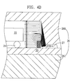
- FIG. 4E it illustrates that the molding compound 29 flashes as no flash preventing mechanism 23 is constructed, and the molding compound 29 is prevented from flashing after the flash preventing mechanisms 23 are disposed, respectively.
- the molding compound 29 prior to forming the flash preventing mechanisms 23 at the entries 270 of the air vents 27 , the molding compound 29 can freely flow to the air vents 27 and easily flash on the substrate 20 .
- the entries 270 are reduced in space due to the construction of the flash preventing mechanisms 23 , the flow rate of the molding compound 29 is accordingly reduced at the entries 270 .
- FIG. 5 Illustrated in FIG. 5 is the second embodiment of the semiconductor package of the invention. As shown in the drawing, this embodiment is substantially identical to the first embodiment, with the only difference in that a TFFCBGA (thin and fine flip chip ball grid array) semiconductor package is exemplified in this embodiment.
- a molded underfill technology is implemented in a longitudinal molding manner, that is, a plurality of air vents 37 are disposed at one end of a mold cavity 362 opposing to a position where an injection runner 364 is formed, in which at an entry 370 of each air vent 37 there is also formed a flash preventing mechanism 33 .
- the air vents 37 are disposed approximately in parallel to a flowing direction of a molding compound 39 , and therefore the flash preventing mechanisms 33 are necessarily formed in front of the air vents 37 , so as to reduce the flow rate of the molding compound 39 and prevent flash of the molding compound 39 from occurrence accordingly.
- the fabricating method of the semiconductor package of the invention can also be applied to a general wire-bonding type BGA semiconductor package 4 .
- the semiconductor package 4 employs a flash preventing mechanism 43 for preventing flash of a molding compound 49 from occurrence, as well as reducing the flow rate of the molding compound 49 , so as to decrease the impact from injection of the molding compound 49 to bonding wires 41 and the occurrence of dislocation for the bonding wires 41 due to the injection impact, and accordingly more various materials can be used as the molding compound 49 .
Abstract
A semiconductor package and a fabricating method thereof are proposed, in which a substrate is prepared for having at least one flash preventing mechanism disposed on a surface of the substrate corresponding to a position in front of an entry of an air vent in a mold. After a semiconductor chip is mounted on the substrate by a plurality of conductive elements, a molding compound having high fluidity and fine filler particles is used to encapsulate the chip and the flash preventing mechanism. As the flash preventing mechanism is disposed in a manner of reducing the entry space of the air vent, the flow of the molding compound is impeded by the flash preventing mechanism, making the molding compound rapidly absorb heat of the mold and accordingly increased in viscosity. This helps prevent flash of the molding compound from occurrence, and assure the semiconductor package in quality and profile.
Description
The present invention relates to semiconductor packages and fabricating methods thereof, and more particularly, to a semiconductor package having a semiconductor chip mounted on a substrate and a fabricating method thereof
A conventional BGA (ball grid array) semiconductor package employs an advanced technology, in which a substrate has a front side for disposing a semiconductor chip thereon and a back side for implanting a plurality of solder balls, so as to provide high density of I/O connections for electrically connecting the semiconductor package to an external printed circuit board.
A FCBGA (flip-chip ball grid array) semiconductor package is more improved than the conventional BGA semiconductor package, in that a semiconductor chip is mounted in the FCBGA semiconductor package in an upside-down manner that the chip has an upper side downwardly reflowed to a front side of a substrate by a plurality of solder bumps, while on a back side of the substrate there are implanted a plurality of solder balls for electrically connecting the semiconductor package to an external device, and accordingly the semiconductor package can be miniaturized in profile.
However, the solder bumps for mounting the chip on the substrate are disposed in a manner that a cavity is formed between the chip and the substrate. If the cavity is not filled with an insulative material, the chip and the substrate tend to be structurally damaged by a thermal stress generated from the difference in coefficient of thermal expansion (CTE) between the chip and the substrate during a temperature cycle in subsequent fabricating processes. Therefore, a flip chip underfill process, which fills the cavity between the chip and the substrate with the insulative material such as epoxy resin, is essential for fabricating the FCBGA semiconductor package, so as to enhance the structural strength for the semiconductor package.
Currently, U.S. Pat. Nos. 5,535,101 “Leadless Integrated Circuit Package” and U.S. Pat. No. 5,218,234 “Semiconductor Device with Controlled Spread Polymeric Underfill” have respectively disclosed a flip chip underfill technology; however, drawbacks have been found for the technology as follows. First, the flip chip underfill technology employs a capillary filling technique, which requires long filling time and tends to cause the formation of voids. Moreover, an ideal material used for filling the cavity between the chip and the substrate is commonly added with a solid filler for making the filling material have a similar CTE to that of the solder bumps, so as to protect the solder bumps from being damaged by a thermal stress. However, the addition of the solid filler significantly increases a viscosity of the filling material, which makes the filling material reduced in fluidity and the filling time further prolonged.
U.S. Pat. No. 6,038,136 discloses a simplified flip chip underfill technology, that is, a molded underfill technology in a molding process. As shown. in FIG. 1, a FCBGA semiconductor package 1 includes a substrate 10 having a front side 100 pre-formed with a chip bonding region 102 thereon for reflowing a semiconductor chip 12 on the chip bonding region 102 in a flip chip manner via a plurality of solder bumps 11; while the substrate 10 has a back side 101 to be covered by a solder mask 16 in a manner that a plurality of solder pads 18 formed on the back side 101 are exposed for implanting a plurality of solder balls (not shown) thereon, and further, a specified molding compound 19 is used for encapsulating the chip 12 and the solder bumps 11. The molding compound 19 is a low viscous epoxy resin containing a solid filler in 70-90%, wherein the solid filler consists of flue particles having small particle diameters within 0.01-0.05 mm such as silicon, quartz, etc.
The foregoing underfill technology is characterized in that the filling for a cavity between the chip 12 and the substrate 10 is implemented in the molding process. As shown in FIG. 2, after a filling material 19 (same as the molding compound 19) is injected into a mold (not shown), excess air can escape through a plurality of air vents 17 connected to the outside for preventing the formation of voids. However, as the filling material 19 having high fluidity and a fine filler with a particle diameter smaller than 20 μm, and the air vents 17 about 40-50 μm in height are much higher than the filler's particle diameter, the low viscous filling material 19 can therefore freely leak out of the air vents 17, making the filling material 19 seriously flash around the air vents 17. In addition, the flashing material 19 can further flow through slots 104 at two sides of the substrate 10 to a bottom surface of the semiconductor package 1, making the mold hard to be removed from the semiconductor package 1 due to the stickiness of the flashing material 19; while the solder pads (not shown) formed on the back side 101 of the substrate 10 can also be easily contaminated by the flashing material 19, and accordingly implantation of the solder balls on the solder pads is deteriorated in quality.
A primary objective of the present invention is to provide a semiconductor package and a fabricating method thereof, in which a flash preventing mechanism is formed at a front end of an air vent, for reducing an entry space of the air vent and accordingly making a molding compound flow slowly into the air vent, so as to help prevent the molding compound from flashing on a surface of a substrate. Moreover, flash of the molding compound can be prevented from occurring on a bottom surface of the semiconductor package in the invention, for allowing a mold to be easily removed after completing a molding process. In addition, the invention allows solder pads formed on the substrate to be free of flash, so as to assure the quality of an implantation process for implanting solder balls on the solder pads.
In accordance with the foregoing and other objectives, the present invention proposes a semiconductor package and a fabricating method thereof, comprising: a substrate having a front side and a back side is prepared, wherein the front side is pre-formed with a chip bonding region, and on the front side around the chip bonding region there are disposed a plurality of flash preventing mechanisms corresponding in position to entries of air vents in a mold; a semiconductor chip is mounted on the chip bonding region and electrically connected to the substrate; and an encapsulant is formed of a molding compound with high fluidity for encapsulating the chip and the flash preventing mechanisms, so that the fabrication for the semiconductor package is completed.
As the flash preventing mechanisms are disposed on the substrate corresponding in position to the entries of the air vents, in a molding process, flow of a molding compound can be impeded by the flash preventing mechanisms at the air vent entries for reducing the flow rate of the molding compound. Further, the flash preventing mechanisms occupy part of the entry spaces at the air vents, making the slower flowing molding compound able to rapid absorb heat from the mold and accordingly increase in viscosity, so as to effectively prevent flash of the molding compound from occurrence.
The present invention can be more fully understood by reading the following detailed description of the preferred embodiments, with reference made to the accompanying drawings wherein:
FIG. 1 (PRIOR ART) is a sectional view of a FCBGA semiconductor package in the use of a molded underfill technology disclosed in U.S. Pat. No. 6,038,136;
FIG. 2 (PRIOR ART) is a top view showing flash of a molding compound in a molding process of FIG. 1;
FIG. 3A is top view of a first preferred embodiment of the semiconductor package of the invention;
FIG. 3B is a sectional view of a first preferred embodiment of the semiconductor package of the invention;
FIGS. 4A-4E are schematic diagrams showing the steps involved in fabricating the semiconductor package of the invention;
FIG. 5 is a top view showing a molding process for the semiconductor package of the invention; and
FIG. 6 is a sectional view of another preferred embodiment of the semiconductor package of the invention.
In the first embodiment, a FCBGA semiconductor package is exemplified for depicting in detail a molded underfill technology used in the semiconductor package of the invention.
Illustrated in FIGS. 3A and 313 are respectively a top view and a sectional view of the FCBGA semiconductor package 2 in the first embodiment of the invention. As shown in the drawing, the FCBGA semiconductor package 2 includes a substrate 20, a semiconductor chip 22 mounted on the substrate 20 in a reflow manner by a plurality of solder bumps 21, a plurality of flash preventing mechanisms 23 disposed on the substrate 20 corresponding in position to front ends of air vents 27 of a mold (not shown), a plurality of solder balls 24 implanted on a back side 201 of the substrate 20 for electrically connecting the chip 22 to an external device, and an encapsulant 29 for encapsulating the chip 22 and the flash preventing mechanisms 23.
Illustrated in FIGS. 4A-4E are the steps involved in fabricating the semiconductor package of the invention.
Referring first to FIG. 4A, a substrate 20 having a front side 200 and a back side 201 is prepared, wherein the front side 200 is preformed with a chip bonding region 202. On the front side 200 of the substrate 20 around the chip bonding region 202 there are formed a plurality of flash preventing mechanisms 23 corresponding in position to front ends of air vents of a mold (not shown), while the flash preventing mechanisms 23 can be blocks made of an adhesive, passive elements such as capacitors, resisters or other electronic elements, or a plurality of solder balls 231 and ball pads 230, in a manner that the solder balls 231 are implanted on the ball pads 230 formed at predetermined positions on the front side 200 of the substrate 20, as shown in FIG. 4B. The solder balls 231 can be made of gold or copper.
Further in FIG. 4A, at least one semiconductor chip 22 is bonded to the chip bonding region 202 on the substrate 20 in a flip chip manner by a plurality of solder bumps 21, while a plurality of solder pads (not shown) are formed on the back side 201 of the substrate 20 for subsequently implanting a plurality of solder balls (not shown) on the solder pads. In this case, the solder bumps 21 for mounting the chip 22 on the substrate 20 are disposed in a manner that a cavity 25 is formed between the chip 22 and the substrate 20, and accordingly a flip chip underfill process is necessarily performed for enhancing joint strength between the solder bumps 21 and the substrate 20.
In the invention, a molded underfill technology is employed, in which formation of an encapsulant 29 and the flip chip underfill process are simultaneously performed in a molding process. Referring to FIG. 4C, the substrate 20 having the chip 22 and the flash preventing mechanisms 23 disposed thereon is placed in a mold 26, which includes an upper mold 260 having a mold cavity 262 for receiving the chip 22, and a lower mold 261 engaged with the upper mold 260. In the mold cavity 262 proximal to comer positions 263 thereof there are formed an injection runner 264 and a plurality of air vents 27 connected to the outside for allowing air in the mold cavity 262 to escape during injecting a molding compound 29 (designated by the same reference numeral as the encapsulant 29). Since the above mentioned is conventional in the art, it will not be further detailed herein. However, it is to be noted that in the invention, at least one flash preventing mechanism 23 for impeding a molding flow of the molding compound 29 is disposed at the front end of each air vent 27 around the corner positions 263 of the mold cavity 262 during molding.
Further in FIG. 4C, in order to shorten the filling and baking time for the flip chip underfill process, the encapsulant 29 for encapsulating the chip 22 is formed of the molding compound 29 such as epoxy resin having high fluidity and fine filler size. When the molding compound 29 flows to the corner positions 263 of the mold cavity 262, the molding flow of the molding compound 29 (indicated as an arrow in FIG. 4D) is slowed down at entries 270 of the air vents 27 due to decrease in space at the entries 270 by the construction of the flash preventing mechanisms 23. This facilitates the molding compound 29 to rapidly absorb heat of the mold 26 for increasing the viscosity thereof, so as to prevent the molding compound 29 from flashing out of the air vents 27.
Referring final to FIG. 4E, it illustrates that the molding compound 29 flashes as no flash preventing mechanism 23 is constructed, and the molding compound 29 is prevented from flashing after the flash preventing mechanisms 23 are disposed, respectively. As shown in the drawing, prior to forming the flash preventing mechanisms 23 at the entries 270 of the air vents 27, the molding compound 29 can freely flow to the air vents 27 and easily flash on the substrate 20. However, as the entries 270 are reduced in space due to the construction of the flash preventing mechanisms 23, the flow rate of the molding compound 29 is accordingly reduced at the entries 270. This therefore can prevent the molding compound 29 from flashing on the back side 201 of the substrate 20, and accordingly the solder pads formed on the back side 201 can be free of contamination from flash, so as to assure the bonding quality of the solder balls to the solder pads and the profile of the semiconductor package.
Illustrated in FIG. 5 is the second embodiment of the semiconductor package of the invention. As shown in the drawing, this embodiment is substantially identical to the first embodiment, with the only difference in that a TFFCBGA (thin and fine flip chip ball grid array) semiconductor package is exemplified in this embodiment. In the TFFCBGA semiconductor package, a molded underfill technology is implemented in a longitudinal molding manner, that is, a plurality of air vents 37 are disposed at one end of a mold cavity 362 opposing to a position where an injection runner 364 is formed, in which at an entry 370 of each air vent 37 there is also formed a flash preventing mechanism 33. In this case, the air vents 37 are disposed approximately in parallel to a flowing direction of a molding compound 39, and therefore the flash preventing mechanisms 33 are necessarily formed in front of the air vents 37, so as to reduce the flow rate of the molding compound 39 and prevent flash of the molding compound 39 from occurrence accordingly.
Except a molded underfill technology, the fabricating method of the semiconductor package of the invention can also be applied to a general wire-bonding type BGA semiconductor package 4. Referring to FIG. 6, the semiconductor package 4 employs a flash preventing mechanism 43 for preventing flash of a molding compound 49 from occurrence, as well as reducing the flow rate of the molding compound 49, so as to decrease the impact from injection of the molding compound 49 to bonding wires 41 and the occurrence of dislocation for the bonding wires 41 due to the injection impact, and accordingly more various materials can be used as the molding compound 49.
The invention has been described using exemplary preferred embodiments. However, it is to be understood that the scope of the invention is not limited to the disclosed embodiments. On the contrary, it is intended to cover various modifications and similar arrangements. The scope of the claims, therefore, should be accorded the broadest interpretation so as to encompass all such modifications and similar arrangements.
Claims (16)
1. A semiconductor package with a flash preventing mechanism, comprising:
a substrate having at least one flash preventing mechanism disposed on a surface of the substrate corresponding to a position in front of an entry of a groove in a mold;
at least one semiconductor chip mounted on the substrate and electrically connected to the substrate; and
an encapsulant formed by a molding compound injected into the mold for encapsulating the semiconductor chip and the flash preventing mechanism;
wherein the flash preventing mechanism reduces a flow rate of the molding compound at the entry of the groove, so as to prevent the molding compound from flashing into the groove.
2. The semiconductor package of claim 1 , wherein the semiconductor package is a BGA (ball grid array) semiconductor package.
3. The semiconductor package of claim 1 , wherein the semiconductor package is a FCBGA (flip chip ball grid array) semiconductor package.
4. The semiconductor package of claim 1 , wherein the groove is an air vent.
5. The semiconductor package of claim 1 , wherein the flash preventing mechanism is a block made of an adhesive, or a passive element such as a capacitor or a resister.
6. The semiconductor package of claim 1 , wherein the flash preventing mechanism includes a solder pad formed on the surface of the substrate and a solder ball implanted on the solder pad.
7. The semiconductor package of claim 1 , wherein the encapsulant is formed of a molding compound having high fluidity and fine particles of a solid filler.
8. The semiconductor package of claim 7 , wherein the particles of the solid filler are much smaller in diameter than a height of the entry of the groove.
9. A fabricating method of a semiconductor package with a flash preventing mechanism, comprising the steps of:
preparing a substrate having at least one flash preventing mechanism disposed on a surface of the substrate corresponding to a position in front of an entry of a groove in a mold;
mounting at least one semiconductor chip on the substrate and electrically connecting the semiconductor chip to the substrate; and
forming an encapsulant formed by a molding compound injected into the mold for encapsulating the semiconductor chip and the flash preventing mechanism;
wherein the flash preventing mechanism reduces a flow rate of the molding compound at the entry of the groove, so as to prevent the molding compound from flashing into the groove.
10. The fabricating method of claim 9 , wherein the semiconductor package is a BGA (ball grid array) semiconductor package.
11. The fabricating method of claim 9 , wherein the semiconductor package is a FCBGA (flip chip ball grid array) semiconductor package.
12. The fabricating method of claim 9 , wherein the groove is an air vent.
13. The fabricating method of claim 9 , wherein the flash preventing mechanism is a block made of an adhesive, or a passive element such as a capacitor or a resister.
14. The fabricating method of claim 9 , wherein the flash preventing mechanism includes a solder pad formed on the surface of the substrate and a solder ball implanted on the solder pad.
15. The fabricating method of claim 9 , wherein the encapsulant is formed of a molding compound having high fluidity and fine particles of a solid filler.
16. The fabricating method of claim 15 , wherein the particles of the solid filler are much smaller in diameter than a height of the entry of the groove.
Priority Applications (1)
| Application Number | Priority Date | Filing Date | Title |
|---|---|---|---|
| US09/932,054 US6555924B2 (en) | 2001-08-18 | 2001-08-18 | Semiconductor package with flash preventing mechanism and fabrication method thereof |
Applications Claiming Priority (1)
| Application Number | Priority Date | Filing Date | Title |
|---|---|---|---|
| US09/932,054 US6555924B2 (en) | 2001-08-18 | 2001-08-18 | Semiconductor package with flash preventing mechanism and fabrication method thereof |
Publications (2)
| Publication Number | Publication Date |
|---|---|
| US20030034568A1 US20030034568A1 (en) | 2003-02-20 |
| US6555924B2 true US6555924B2 (en) | 2003-04-29 |
Family
ID=25461697
Family Applications (1)
| Application Number | Title | Priority Date | Filing Date |
|---|---|---|---|
| US09/932,054 Expired - Lifetime US6555924B2 (en) | 2001-08-18 | 2001-08-18 | Semiconductor package with flash preventing mechanism and fabrication method thereof |
Country Status (1)
| Country | Link |
|---|---|
| US (1) | US6555924B2 (en) |
Cited By (14)
| Publication number | Priority date | Publication date | Assignee | Title |
|---|---|---|---|---|
| US20050029642A1 (en) * | 2003-07-30 | 2005-02-10 | Minoru Takaya | Module with embedded semiconductor IC and method of fabricating the module |
| US20050227409A1 (en) * | 2004-04-13 | 2005-10-13 | Taiwan Semiconductor Manufacturing Co., Ltd. | Microelectronics package assembly tool and method of manufacture therewith |
| US20050269384A1 (en) * | 2004-06-04 | 2005-12-08 | Inventec Corporation | Method of preventing flashing between solder pads on circuit board |
| US20060057341A1 (en) * | 2004-09-16 | 2006-03-16 | Tdk Corporation | Multilayer substrate and manufacturing method thereof |
| US7042072B1 (en) * | 2002-08-02 | 2006-05-09 | Amkor Technology, Inc. | Semiconductor package and method of manufacturing the same which reduces warpage |
| US20060135024A1 (en) * | 2004-12-22 | 2006-06-22 | Thomas Oomman P | High performance elastic materials made using styrene block copolymers and mixtures |
| US20060208364A1 (en) * | 2005-03-19 | 2006-09-21 | Chien-Jen Wang | LED device with flip chip structure |
| US20080308949A1 (en) * | 2007-06-18 | 2008-12-18 | Seong Cheol Kim | Flip chip package and method for manufacturing the same |
| US7544537B2 (en) | 2005-09-28 | 2009-06-09 | Tdk Corporation | Semiconductor IC-embedded substrate and method for manufacturing same |
| US20090242255A1 (en) * | 2008-03-27 | 2009-10-01 | Ibiden Co., Ltd | Wiring board with built-in electronic component and method of manufacturing same |
| US20100001410A1 (en) * | 2008-07-02 | 2010-01-07 | Teck-Gyu Kang | Flip chip overmold package |
| US20100052150A1 (en) * | 2007-11-16 | 2010-03-04 | Seng Guan Chow | Integrated circuit package system with package substrate having corner contacts and method of manufacture thereof |
| US20180358237A1 (en) * | 2017-06-09 | 2018-12-13 | Advanced Semiconductor Engineering, Inc. | Semiconductor device package |
| CN111546568A (en) * | 2019-02-08 | 2020-08-18 | 精工爱普生株式会社 | Method for manufacturing electronic device |
Families Citing this family (7)
| Publication number | Priority date | Publication date | Assignee | Title |
|---|---|---|---|---|
| US6969918B1 (en) * | 2001-08-30 | 2005-11-29 | Micron Technology, Inc. | System for fabricating semiconductor components using mold cavities having runners configured to minimize venting |
| US7233057B2 (en) * | 2004-05-28 | 2007-06-19 | Nokia Corporation | Integrated circuit package with optimized mold shape |
| US7147447B1 (en) * | 2005-07-27 | 2006-12-12 | Texas Instruments Incorporated | Plastic semiconductor package having improved control of dimensions |
| JP2008004570A (en) * | 2006-06-20 | 2008-01-10 | Matsushita Electric Ind Co Ltd | Process and apparatus for manufacturing resin sealed semiconductor device, and resin sealed semiconductor device |
| JP5265438B2 (en) * | 2009-04-01 | 2013-08-14 | 新光電気工業株式会社 | Semiconductor device |
| JP5154516B2 (en) * | 2009-05-22 | 2013-02-27 | シャープ株式会社 | Solar cell module and method for manufacturing solar cell module |
| TWI420623B (en) * | 2010-10-08 | 2013-12-21 | Powertech Technology Inc | Molding method and mold jig for preventing air trap effect on a substrate strip |
Citations (12)
| Publication number | Priority date | Publication date | Assignee | Title |
|---|---|---|---|---|
| US5450283A (en) * | 1992-11-03 | 1995-09-12 | Motorola, Inc. | Thermally enhanced semiconductor device having exposed backside and method for making the same |
| US5535101A (en) | 1992-11-03 | 1996-07-09 | Motorola, Inc. | Leadless integrated circuit package |
| US5672912A (en) * | 1995-11-21 | 1997-09-30 | Sharp Kabushiki Kaisha | Resin-sealed type semiconductor device and method for manufacturing the same |
| US5844309A (en) * | 1995-03-20 | 1998-12-01 | Fujitsu Limited | Adhesive composition, semiconductor device using the composition and method for producing a semiconductor device using the composition |
| US6038136A (en) | 1997-10-29 | 2000-03-14 | Hestia Technologies, Inc. | Chip package with molded underfill |
| US6104095A (en) * | 1997-07-03 | 2000-08-15 | Samsung Electronics Co., Ltd. | Printed circuit board and chip-on-board packages using same |
| US6246115B1 (en) * | 1998-10-21 | 2001-06-12 | Siliconware Precision Industries Co., Ltd. | Semiconductor package having a heat sink with an exposed surface |
| US6319450B1 (en) * | 1999-07-12 | 2001-11-20 | Agere Systems Guardian Corp. | Encapsulated circuit using vented mold |
| US6329606B1 (en) * | 1996-04-24 | 2001-12-11 | Amkor Technology, Inc. | Grid array assembly of circuit boards with singulation grooves |
| US20020003308A1 (en) * | 1998-05-13 | 2002-01-10 | Jae-Hong Kim | Semiconductor chip package and method for fabricating the same |
| US6369455B1 (en) * | 2000-01-04 | 2002-04-09 | Siliconware Precision Industries Co., Ltd. | Externally-embedded heat-dissipating device for ball grid array integrated circuit package |
| US6407461B1 (en) * | 1997-06-27 | 2002-06-18 | International Business Machines Corporation | Injection molded integrated circuit chip assembly |
-
2001
- 2001-08-18 US US09/932,054 patent/US6555924B2/en not_active Expired - Lifetime
Patent Citations (12)
| Publication number | Priority date | Publication date | Assignee | Title |
|---|---|---|---|---|
| US5450283A (en) * | 1992-11-03 | 1995-09-12 | Motorola, Inc. | Thermally enhanced semiconductor device having exposed backside and method for making the same |
| US5535101A (en) | 1992-11-03 | 1996-07-09 | Motorola, Inc. | Leadless integrated circuit package |
| US5844309A (en) * | 1995-03-20 | 1998-12-01 | Fujitsu Limited | Adhesive composition, semiconductor device using the composition and method for producing a semiconductor device using the composition |
| US5672912A (en) * | 1995-11-21 | 1997-09-30 | Sharp Kabushiki Kaisha | Resin-sealed type semiconductor device and method for manufacturing the same |
| US6329606B1 (en) * | 1996-04-24 | 2001-12-11 | Amkor Technology, Inc. | Grid array assembly of circuit boards with singulation grooves |
| US6407461B1 (en) * | 1997-06-27 | 2002-06-18 | International Business Machines Corporation | Injection molded integrated circuit chip assembly |
| US6104095A (en) * | 1997-07-03 | 2000-08-15 | Samsung Electronics Co., Ltd. | Printed circuit board and chip-on-board packages using same |
| US6038136A (en) | 1997-10-29 | 2000-03-14 | Hestia Technologies, Inc. | Chip package with molded underfill |
| US20020003308A1 (en) * | 1998-05-13 | 2002-01-10 | Jae-Hong Kim | Semiconductor chip package and method for fabricating the same |
| US6246115B1 (en) * | 1998-10-21 | 2001-06-12 | Siliconware Precision Industries Co., Ltd. | Semiconductor package having a heat sink with an exposed surface |
| US6319450B1 (en) * | 1999-07-12 | 2001-11-20 | Agere Systems Guardian Corp. | Encapsulated circuit using vented mold |
| US6369455B1 (en) * | 2000-01-04 | 2002-04-09 | Siliconware Precision Industries Co., Ltd. | Externally-embedded heat-dissipating device for ball grid array integrated circuit package |
Cited By (27)
| Publication number | Priority date | Publication date | Assignee | Title |
|---|---|---|---|---|
| US7042072B1 (en) * | 2002-08-02 | 2006-05-09 | Amkor Technology, Inc. | Semiconductor package and method of manufacturing the same which reduces warpage |
| US20050029642A1 (en) * | 2003-07-30 | 2005-02-10 | Minoru Takaya | Module with embedded semiconductor IC and method of fabricating the module |
| US7547975B2 (en) * | 2003-07-30 | 2009-06-16 | Tdk Corporation | Module with embedded semiconductor IC and method of fabricating the module |
| US20050227409A1 (en) * | 2004-04-13 | 2005-10-13 | Taiwan Semiconductor Manufacturing Co., Ltd. | Microelectronics package assembly tool and method of manufacture therewith |
| US7098082B2 (en) | 2004-04-13 | 2006-08-29 | Taiwan Semiconductor Manufacturing Company, Ltd. | Microelectronics package assembly tool and method of manufacture therewith |
| US20050269384A1 (en) * | 2004-06-04 | 2005-12-08 | Inventec Corporation | Method of preventing flashing between solder pads on circuit board |
| US20060057341A1 (en) * | 2004-09-16 | 2006-03-16 | Tdk Corporation | Multilayer substrate and manufacturing method thereof |
| US7868464B2 (en) | 2004-09-16 | 2011-01-11 | Tdk Corporation | Multilayer substrate and manufacturing method thereof |
| US20060135024A1 (en) * | 2004-12-22 | 2006-06-22 | Thomas Oomman P | High performance elastic materials made using styrene block copolymers and mixtures |
| US20060208364A1 (en) * | 2005-03-19 | 2006-09-21 | Chien-Jen Wang | LED device with flip chip structure |
| US7544537B2 (en) | 2005-09-28 | 2009-06-09 | Tdk Corporation | Semiconductor IC-embedded substrate and method for manufacturing same |
| US20090298229A1 (en) * | 2007-06-18 | 2009-12-03 | Seong Cheol Kim | Flip chip package and method for manufacturing the same |
| US20080308949A1 (en) * | 2007-06-18 | 2008-12-18 | Seong Cheol Kim | Flip chip package and method for manufacturing the same |
| US20100052150A1 (en) * | 2007-11-16 | 2010-03-04 | Seng Guan Chow | Integrated circuit package system with package substrate having corner contacts and method of manufacture thereof |
| US7863726B2 (en) * | 2007-11-16 | 2011-01-04 | Stats Chippac Ltd. | Integrated circuit package system with package substrate having corner contacts and method of manufacture thereof |
| US8347493B2 (en) * | 2008-03-27 | 2013-01-08 | Ibiden Co., Ltd. | Wiring board with built-in electronic component and method of manufacturing same |
| US20090242255A1 (en) * | 2008-03-27 | 2009-10-01 | Ibiden Co., Ltd | Wiring board with built-in electronic component and method of manufacturing same |
| WO2010002969A3 (en) * | 2008-07-02 | 2010-05-06 | Altera Corporation | Flip chip overmold package |
| US20100001410A1 (en) * | 2008-07-02 | 2010-01-07 | Teck-Gyu Kang | Flip chip overmold package |
| US8415809B2 (en) | 2008-07-02 | 2013-04-09 | Altera Corporation | Flip chip overmold package |
| US9054023B1 (en) | 2008-07-02 | 2015-06-09 | Altera Corporation | Flip chip overmold package |
| US20180358237A1 (en) * | 2017-06-09 | 2018-12-13 | Advanced Semiconductor Engineering, Inc. | Semiconductor device package |
| US10586716B2 (en) * | 2017-06-09 | 2020-03-10 | Advanced Semiconductor Engineering, Inc. | Semiconductor device package |
| US11164756B2 (en) | 2017-06-09 | 2021-11-02 | Advanced Semiconductor Engineering, Inc. | Semiconductor device package having continously formed tapered protrusions |
| CN111546568A (en) * | 2019-02-08 | 2020-08-18 | 精工爱普生株式会社 | Method for manufacturing electronic device |
| CN111546568B (en) * | 2019-02-08 | 2022-03-22 | 精工爱普生株式会社 | Method for manufacturing electronic device |
| US11376770B2 (en) * | 2019-02-08 | 2022-07-05 | Seiko Epson Corporation | Method of manufacturing electronic device |
Also Published As
| Publication number | Publication date |
|---|---|
| US20030034568A1 (en) | 2003-02-20 |
Similar Documents
| Publication | Publication Date | Title |
|---|---|---|
| US6555924B2 (en) | Semiconductor package with flash preventing mechanism and fabrication method thereof | |
| US6495083B2 (en) | Method of underfilling an integrated circuit chip | |
| US6560122B2 (en) | Chip package with molded underfill | |
| US6038136A (en) | Chip package with molded underfill | |
| JP3313067B2 (en) | Method and apparatus for injection mold flip chip encapsulation | |
| US6486562B1 (en) | Circuit device with bonding strength improved and method of manufacturing the same | |
| US6459144B1 (en) | Flip chip semiconductor package | |
| US6507104B2 (en) | Semiconductor package with embedded heat-dissipating device | |
| US6282094B1 (en) | Ball-grid array integrated circuit package with an embedded type of heat-dissipation structure and method of manufacturing the same | |
| US6933176B1 (en) | Ball grid array package and process for manufacturing same | |
| US7339278B2 (en) | Cavity chip package | |
| US20050263906A1 (en) | Electronic system including a semiconductor device with at least one semiconductor die, a carrier, and an encapsulant that fills a space between the die and the carrier and covers intermediate conductive elements that connect the die and the carrier | |
| US6867487B2 (en) | Flash-preventing semiconductor package | |
| US20080093733A1 (en) | Chip package and manufacturing method thereof | |
| US20020086500A1 (en) | Semiconductor package and fabricating method thereof | |
| US20050110168A1 (en) | Low coefficient of thermal expansion (CTE) semiconductor packaging materials | |
| US20020095192A1 (en) | Method of fabricating a flip-chip ball-grid-array package with molded underfill | |
| KR20040030659A (en) | Chip lead frames | |
| US20110084375A1 (en) | Semiconductor device package with integrated stand-off | |
| US20060076695A1 (en) | Semiconductor package with flash-absorbing mechanism and fabrication method thereof | |
| JP2907188B2 (en) | Semiconductor device, method of mounting semiconductor device, and method of manufacturing semiconductor device | |
| US8030768B2 (en) | Semiconductor package with under bump metallization aligned with open vias | |
| US20050077080A1 (en) | Ball grid array (BGA) package having corner or edge tab supports | |
| KR100674501B1 (en) | Method for attaching semiconductor chip using flip chip bonding technic | |
| JP3857574B2 (en) | Semiconductor device and manufacturing method thereof |
Legal Events
| Date | Code | Title | Description |
|---|---|---|---|
| AS | Assignment |
Owner name: SILICONWARE PRECISION INDUSTRIES CO., LTD., TAIWAN Free format text: ASSIGNMENT OF ASSIGNORS INTEREST;ASSIGNORS:CHAI, TING KE;YUAN, PO HAUU;PU, HAN PIN;REEL/FRAME:012102/0816 Effective date: 20010704 |
|
| STCF | Information on status: patent grant |
Free format text: PATENTED CASE |
|
| FPAY | Fee payment |
Year of fee payment: 4 |
|
| FPAY | Fee payment |
Year of fee payment: 8 |
|
| FPAY | Fee payment |
Year of fee payment: 12 |