US6560290B2 - CMOS driver and on-chip termination for gigabaud speed data communication - Google Patents
CMOS driver and on-chip termination for gigabaud speed data communication Download PDFInfo
- Publication number
- US6560290B2 US6560290B2 US09/234,619 US23461999A US6560290B2 US 6560290 B2 US6560290 B2 US 6560290B2 US 23461999 A US23461999 A US 23461999A US 6560290 B2 US6560290 B2 US 6560290B2
- Authority
- US
- United States
- Prior art keywords
- coupled
- node
- receiver
- data signal
- data
- Prior art date
- Legal status (The legal status is an assumption and is not a legal conclusion. Google has not performed a legal analysis and makes no representation as to the accuracy of the status listed.)
- Expired - Lifetime
Links
Images


Classifications
-
- H—ELECTRICITY
- H04—ELECTRIC COMMUNICATION TECHNIQUE
- H04L—TRANSMISSION OF DIGITAL INFORMATION, e.g. TELEGRAPHIC COMMUNICATION
- H04L25/00—Baseband systems
- H04L25/02—Details ; arrangements for supplying electrical power along data transmission lines
- H04L25/0264—Arrangements for coupling to transmission lines
- H04L25/028—Arrangements specific to the transmitter end
-
- H—ELECTRICITY
- H04—ELECTRIC COMMUNICATION TECHNIQUE
- H04L—TRANSMISSION OF DIGITAL INFORMATION, e.g. TELEGRAPHIC COMMUNICATION
- H04L25/00—Baseband systems
- H04L25/02—Details ; arrangements for supplying electrical power along data transmission lines
- H04L25/0264—Arrangements for coupling to transmission lines
- H04L25/0292—Arrangements specific to the receiver end
-
- H—ELECTRICITY
- H04—ELECTRIC COMMUNICATION TECHNIQUE
- H04L—TRANSMISSION OF DIGITAL INFORMATION, e.g. TELEGRAPHIC COMMUNICATION
- H04L25/00—Baseband systems
- H04L25/02—Details ; arrangements for supplying electrical power along data transmission lines
- H04L25/0264—Arrangements for coupling to transmission lines
- H04L25/0272—Arrangements for coupling to multiple lines, e.g. for differential transmission
Definitions
- This invention relates to data communication systems. More particularly, this invention relates high-speed communications systems including high-speed transmitters and receivers.
- Such transmission lines typically include only one or two conductors, in contrast with the 64-bit and wider data paths within computing systems now commonly available.
- a communication system that includes oversampling is often utilized to recover transmitted data.
- Such a system includes a receiver which samples the incoming serial data stream at a rate greater than the rate at which symbols (bits) are being transmitted. For example, in a three-times (3 ⁇ ) oversampling receiver, the incoming data stream is sampled at a rate approximately three times the symbol rate.
- parasitic capacitance and inductance typically introduce substantial distortion into the received signal.
- the physical layer of the Gigabit Ethernet standard requires a so-called PHY chip which operates at gigabaud speeds.
- PHY chip which operates at gigabaud speeds.
- GaAs or bipolar techniques have been used to implement such PHY chips.
- GaAs and bipolar circuits cannot be easily integrated with other CMOS (complementary metal-oxide-semiconductor) circuits and are typically more costly to manufacture than CMOS circuits.
- CMOS driver operating at gigabaud speeds.
- Such a driver may be manufactured more easily than drivers that use GaAs or bipolar techniques and further may be easily integrated with other CMOS circuits.
- a communication system utilizing the gigabaud CMOS driver may additionally include a receiver with on-chip termination to significantly reduce distortion in the presence of parasitic capacitance in inductance in comparison to a receiver with external termination.
- the communication system may include a phase tracker and a frame aligner.
- the phase tracker continously monitors the most frequent transition edges in the oversampled data so that the phase of the receiver clock keeps track of the sender clock.
- the frame aligner comprises a comma detector which enables instant synchronization of data words with a single comma character within a serial data stream.
- FIG. 1 shows a block diagram of a communication system utilizing a gigabaud CMOS driver in accordance with a preferred embodiment of the present invention.
- FIG. 2 shows a circuit diagram of a high-speed serializer in accordance with a preferred embodiment of the present invention.
- FIG. 3 shows a circuit diagram of a differential voltage driver in accordance with a preferred embodiment of the present invention.
- FIG. 4 shows typical circuit configurations of (a) a current mode driver and (b) a voltage mode driver in accordance with a preferred embodiment of the present invention.
- FIG. 5 shows simulated waveforms under the configurations shown in FIG. 4 in accordance with a preferred embodiment of the present invention.
- FIG. 6 shows a circuit diagram of an on-chip termination circuit in accordance with a preferred embodiment of the present invention.
- FIG. 7 shows the characteristics of the on-chip termination circuit shown in FIG. 6 for a 75 ohm transmission line in accordance with a preferred embodiment of the present invention.
- FIG. 8 contrasts (a) a conventional receiver configuration using external termination outside the conventional receiver with (b) the receiver configuration which utilizes on-chip termination within the receiver in accordance with a preferred embodiment of the present invention.
- FIG. 9 contrasts (a) a simulated waveform in a receiver using external termination in accordance with FIG. 8 ( a ) with (b) a simulated waveform in a receiver utilizing on-chip termination in accordance with FIG. 8 ( b ).
- FIG. 10 shows a block diagram of (a) a phase tracker and (b) a frame aligner in accordance with a preferred embodiment of the present invention.
- FIG. 1 shows a block diagram of a communication system 100 utilizing a gigabaud CMOS driver 108 in accordance with a preferred embodiment of the present invention.
- the system 100 includes a transmitter (TX) 102 , a receiver (RX) 104 , and a phase-locked loop (PLL) 106 .
- TX transmitter
- RX receiver
- PLL phase-locked loop
- the transmitter 102 outputs a 1.25 gigabit per second (Gbps) signal to a transmission medium.
- Gbps gigabit per second
- the transmitter 102 includes a differential voltage driver (the gigabaud CMOS driver) 108 , a serializer 110 , and a data retimer 112 .
- the data retimer 112 receives a 125 MHz external clock and a DC-balanced and limited run-length 10-bit parallel data stream from an encoder.
- the data retimer 112 utilizes the external clock to adjust the timing of the data stream.
- the serializer 110 receives the adjusted 10-bit parallel data stream from the data retimer 112 .
- the serializer 110 also receives 10 phase clocks from the PLL 106 .
- the serializer 110 utilizes the 10 phase clocks to transform the 10-bit parallel data stream into a serial bit stream.
- the differential voltage driver 108 receives the serial bit stream from the serializer 110 .
- the differential voltage driver 108 drives the serial bit stream onto the medium at 1.25 Gbps, 10 times the 125 MHz speed of the external clock.
- the transmission medium which carries the 1.25 Gbps signal is not terminated with a conventional external resistor. Instead, the transmission medium is terminated by an on-chip termination circuit 114 within the receiver 104 . Use of the on-chip termination circuit 114 reduces signal distortion in comparison with external termination.
- the receiver 104 includes, in addition to the on-chip termination 114 , a 3-times (3 ⁇ ) oversampler 116 , a phase tracker 118 , a RX clock selector 120 , and a frame aligner 122 .
- the oversampler 116 receives the data signal from the on-chip termination 114 .
- the oversampler 116 utilizes 30 phase clocks supplied by the PLL 106 to oversample the data signal and generate 30 sampled bits in parallel.
- the 3 ⁇ oversampler 116 provides the 30 sampled bits in parallel to the phase tracker 118 .
- the phase tracker 118 and the RX clock selector 120 operate to recover the clock and the data from the oversampled data and provides the recovered data stream to the frame aligner 122 .
- the frame aligner 122 searches for a comma character in the recovered data stream and makes a near instant alignment of the boundary between words when such a comma character is found.
- a clock frequency difference between the TX 102 and the RX 104 of less than 0.1% is to be tolerated.
- the PLL 106 operates to keep the clock frequency difference within that tolerance.
- FIG. 2 shows a circuit diagram of a high-speed serializer 110 in accordance with a preferred embodiment of the present invention.
- the serializer 110 comprises NMOS (n-type metal-oxide-semiconductor) transistors used as switching elements, and PMOS (p-type metal-oxide-semiconductor) transistors (M 1 , M 2 , M 3 ) used as loads. These transistors are used to form differential pseudo-NMOS logic.
- M 1 has its source coupled to a supply voltage, its gate coupled to an electrical ground, and its drain coupled to the sources of M 2 and M 3 . Operationally, M 1 pulls down the common mode voltage so that the output voltage moves around one-half the supply voltage (Vdd/2) with a small swing.
- M 2 has its gate coupled to an electrical ground, and its drain coupled to a first NMOS transistor network 202 .
- M 3 has its gate coupled to an electrical ground, and its drain coupled to a second NMOS transistor network 204 .
- the first network 202 includes a first node 206 coupled to the drain of M 2 .
- the first node 206 is also coupled to the negative input terminal of the differential voltage driver 108 .
- the first node 206 is coupled to ten columns ( 210 , 211 , . . . , 219 ) of NMOS transistors.
- Each column 210 - 219 includes three NMOS transistors in series between the first node 206 and electrical ground.
- the first column 210 includes a first NMOS transistor 210 a whose source is coupled to the first node 206 , a second NMOS transistor 210 b whose source is coupled to the drain of the first NMOS transistor 210 a , and a third NMOS transistor 210 c whose source is coupled to the drain of the second NMOS transistor 210 b and whose drain is coupled to an electrical ground.
- the gate of the first NMOS transistor 210 a is coupled to receive a fifth phase clock signal (ck 4 ) from the PLL 106 .
- the gate of the second NMOS transistor 210 b is coupled to receive a first phase clock signal (ck 0 ) from the PLL 106 .
- the gate of the third NMOS transistor 210 c is coupled to receive a first data signal (d 0 ) from the data retimer 112 .
- the second column 211 includes three NMOS transistors ( 211 a - 211 c ) coupled in series between the first node 206 and an electrical ground.
- the gate of the first NMOS transistor 211 a is coupled to receive a sixth phase clock signal (ck 5 ) from the PLL 106 .
- the gate of the second NMOS transistor 211 b is coupled to receive a second phase clock signal (ck 1 ) from the PLL 106 .
- the gate of the third NMOS transistor 211 c is coupled to receive a second data signal (d 1 ) from the data retimer 112 .
- the gate of the first NMOS transistor 219 a is coupled to receive a fourth phase clock signal (ck 3 ) from the PLL 106 .
- the gate of the second NMOS transistor 219 b is coupled to receive a tenth phase clock signal (ck 9 ) from the PLL 106 .
- the gate of the third NMOS transistor 219 c is coupled to receive a tenth data signal (d 9 ) from the data retimer 112 .
- the second network 204 includes a second node 208 coupled to the drain of M 3 .
- the second node 208 is also coupled to the positive input terminal of the differential voltage driver 108 .
- the second node 208 is coupled to ten columns ( 220 , 221 , . . . , 229 ) of NMOS transistors.
- Each column 220 - 229 includes three NMOS transistors in series between the second node 208 and electrical ground.
- the first column 220 includes a first NMOS transistor 220 a whose source is coupled to the second node 208 , a second NMOS transistor 220 b whose source is coupled to the drain of the first NMOS transistor 220 a , and a third NMOS transistor 220 c whose source is coupled to the drain of the second NMOS transistor 220 b and whose drain is coupled to an electrical ground.
- the gate of the first NMOS transistor 220 a is coupled to receive a fifth phase clock signal (ck 4 ) from the PLL 106 .
- the gate of the second NMOS transistor 220 b is coupled to receive the first phase clock signal (ck 0 ) from the PLL 106 .
- the gate of the third NMOS transistor 220 c is coupled to receive an inverted version of the first data signal (inverted d 0 ) from the data retimer 112 .
- the second column 221 includes three NMOS transistors ( 221 a - 221 c ) coupled in series between the second node 208 and an electrical ground.
- the gate of the first NMOS transistor 221 a is coupled to receive a sixth phase clock signal (ck 5 ) from the PLL 106 .
- the gate of the second NMOS transistor 221 b is coupled to receive a second phase clock signal (ck 1 ) from the PLL 106 .
- the gate of the third NMOS transistor 221 c is coupled to receive an inverted version of the second data signal (inverted d 1 ) from the data retimer 112 .
- the gate of the first NMOS transistor 229 a is coupled to receive a fourth phase clock signal (ck 3 ) from the PLL 106 .
- the gate of the second NMOS transistor 229 b is coupled to receive a tenth phase clock signal (ck 9 ) from the PLL 106 .
- the gate of the third NMOS transistor 229 c is coupled to receive an inverted version of the tenth data signal (d 9 ) from the data retimer 112 .
- FIG. 3 shows a circuit diagram of a differential voltage driver 108 in accordance with a preferred embodiment of the present invention.
- the communication system 100 uses such a differential voltage driver 108 instead of a current mode driver, because a current mode driver is not appropriate to drive a high speed signal onto a transmission line in the presence of large parasitic capacitance and inductance due to bonding wires and pads.
- the differential voltage driver 108 comprises a first inverter circuit 302 a and a second inverter circuit 302 b.
- the first inverter circuit 302 a comprises a NMOS transistor M 1 , a PMOS transistor M 2 , and an inverter 304 a .
- the NMOS transistor M 1 has its gate coupled to a supply voltage, its drain coupled to a first node 306 a , and its source coupled to a second node 308 a .
- the PMOS transistor M 2 has its gate coupled to an electrical ground, its drain coupled to the first node 306 a , and its source coupled to the second node 308 a .
- the inverter 304 a has its input coupled to the first node 306 a and its output coupled to the second node 308 a .
- the first node 306 a is also coupled to receive the negative polarity ( ⁇ ) output from the serializer 110 .
- the second node 308 a is also coupled to output a positive polarity (+) output to the transmission medium (for example, a cable).
- the circuitry of the first inverter circuit 302 a operates to receive the negative polarity data signal from the serializer 110 , invert the signal, and output a positive polarity data signal to the transmission medium.
- M 1 and M 2 are used as feedback resistors which reduce the voltage swing of the inverter 304 a as well as reducing the output impedance.
- the second inverter circuit 302 b comprises a NMOS transistor M 1 , a PMOS transistor M 2 , and an inverter 304 b .
- the NMOS transistor M 1 has its gate coupled to a supply voltage, its drain coupled to a first node 306 b , and its source coupled to a second node 308 b .
- the PMOS transistor M 2 has its gate coupled to an electrical ground, its drain coupled to the first node 306 b , and its source coupled to the second node 308 b .
- the inverter 304 b has its input coupled to the first node 306 b and its output coupled to the second node 308 b .
- the first node 306 b is also coupled to receive the positive polarity (+) output from the serializer 110 .
- the second node 308 b is also coupled to output a negative polarity ( ⁇ ) output to the transmission medium (for example, a cable).
- the circuitry of the second inverter circuit 302 b operates to receive the positive polarity data signal from the serializer 110 , invert the signal, and output a negative polarity data signal to the transmission medium.
- M 1 and M 2 are used as feedback resistors which reduce the voltage swing of the inverter 304 b as well as reducing the output impedance.
- FIG. 4 shows typical circuit configurations of (a) a current mode driver 408 and (b) a voltage mode driver 108 .
- the voltage mode driver 108 would be in accordance with a preferred embodiment of the present invention.
- the driver ( 408 or 108 ) is coupled to a transmission medium via a connection typically including bonding and wire pads.
- the transmission medium and connection thereto are modeled by two capacitors C 1 and C 2 and an inductor L for each of two lines.
- C 2 represents the capacitance of each transmission line, and each of the capacitors C 2 is coupled between a transmission line and an electrical ground.
- Each LC circuit (comprising inductor L and capacitor C 1 ) represents the parasitic inductance and capacitance due to the bonding wires and pads.
- the other end of the transmission medium is coupled to a receiver via an appropriate connection (including termination). The appropriate connection varies depending upon whether the driver is a current mode driver 408 or a voltage mode driver 108 .
- FIG. 5 shows simulated waveforms under the configurations shown in FIG. 4 in accordance with a preferred embodiment of the present invention.
- the inductance L was set to be 4nH, and the two capacitors C 1 and C 2 were set to be 2 pF and 4 pF, respectively.
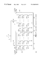
- FIG. 6 shows a circuit diagram of an on-chip termination circuit 114 in accordance with a preferred embodiment of the present invention.
- the on-chip termination circuit is based on a common gate CMOS configuration.
- the on-chip termination circuit 114 includes an internal voltage divider 602 , an impedance matching bias circuit 604 , an external resistor 606 , and a configuration of common gate MOS transistors 608 .
- the internal voltage divider 602 includes four resistors ( 610 , 612 , 614 , 616 ) and three nodes (V h , V m , and V l ).
- the four resistors are coupled in series between a supply voltage and an electrical ground.
- the three nodes exist between the four resistors.
- the first resistor 610 couples the supply voltage to the first node V h .
- the second resistor 612 couples the first node V h to the second node V m .
- the third resistor 614 couples the second node V m to the third node V l .
- the fourth resistor 616 couples the third node V l to an electrical ground.
- each of the three nodes is coupled to the bias circuit 604 .
- the internal voltage divider 602 generates three reference voltages.
- the bias circuit 604 includes three operational amplifiers (opamps) 618 , 620 , and 622 and 7 transistors (M 0 -M 6 ).
- the first opamp 618 has its negative terminal coupled to V m of the voltage divider 602 , its positive terminal coupled to a first node 624 , and its output terminal coupled to a second node 626 .
- the second opamp 620 has its positive terminal coupled to of the voltage divider 602 , its negative terminal coupled to a third node 628 , and its output terminal coupled to a fourth node 630 .
- the fourth node 630 is also labeled as voltage V p .
- the third opamp 622 has its positive terminal coupled to V l , its negative terminal coupled to a fifth node 632 , and its output terminal coupled to a sixth node 634 .
- the sixth node 634 is also labeled as voltage V N .
- the first transistor MO comprises a PMOS transistor having its source coupled to a supply voltage, its drain coupled to the first node 624 , and its gate coupled to the second node 626 .
- the second transistor M 1 comprises a PMOS transistor having its source coupled to a supply voltage, its drain coupled to a seventh node 636 , and its gate coupled to the second node 626 .
- the third transistor M 2 comprises a PMOS transistor having its source coupled to a supply voltage, its drain coupled to the third node 628 , and its gate coupled to the second node 626 .
- each of the first three transistors M 0 -M 2 comprise PMOS transistor having their gates controlled by the output of the first opamp 618 .
- the fourth transistor M 3 comprises a NMOS transistor having its source coupled to a supply voltage, its drain coupled to the fifth node 632 , and its gate coupled to the sixth node 634 (V N ).
- the fifth transistor M 4 comprises a PMOS transistor having its source coupled to the third node 628 , its drain coupled to an electrical ground, and its gate coupled to the fourth node 630 (V P ).
- the sixth transistor M 5 comprises a NMOS transistor having its source and its gate both coupled to the seventh node 636 , and its drain coupled to an electrical ground.
- the seventh transistor M 6 comprises a NMOS transistor having its source coupled to the fifth node 632 , its drain coupled to an electrical ground, and its gate coupled to the seventh node 636 .
- the external resistor 606 includes a resistor, denoted as having a resistance value of Re, coupled between the first node 624 of the bias circuit 604 and an electrical ground.
- the external resistor 606 is used as a reference impedance.
- the common gate MOS transistors 608 include two NMOS transistors M 7 and M 9 , and two PMOS transistors M 8 and M 0 .
- the first NMOS transistor M 7 has its source coupled to a supply voltage, its drain coupled to a first output node 638 , and its gate coupled to the sixth node 634 of the bias circuit 604 .
- the first PMOS transistor M 8 has its source coupled to the first output node 638 , its drain coupled to an electrical ground, and its gate coupled to the fourth node 630 of the bias circuit 604 .
- the first output node 638 is coupled to the positive polarity line from the transmission medium for termination purposes.
- the second NMOS transistor M 9 has its source coupled to a supply voltage, its drain coupled to a second output node 640 , and its gate coupled to the sixth node 634 of the bias circuit 604 .
- the second PMOS transistor M 10 has its source coupled to the second output node 640 , its drain coupled to an electrical ground, and its gate coupled to the fourth node 630 of the bias circuit 604 .
- the second output node 640 is coupled to the negative polarity line of the transmission medium for termination purposes.
- the bias circuit 604 controls the termination voltage and impedance by providing bias voltages V P and V N to the gates of the common gate MOS transistors 608 .
- transistors M 0 , M 1 , M 2 , M 5 and M 6 are connected as current mirrors. All currents in the current mirrors are set as V m /Re.
- Transistors M 7 and M 9 are replicas of M 3 .
- Transistors M 8 and M 10 are replicas of M 4 .
- M 3 generates current Io at V l .
- M 4 generates current Io at V h .
- FIG. 7 shows the characteristics of the on-chip termination circuit 114 shown in FIG. 6 for a 75 ohm transmission line in accordance with a preferred embodiment of the present invention. Both voltage 702 and current 704 characteristics are shown. In addition, a voltage versus current graph 706 is also shown.
- the voltage vs. current graph 706 shows net current 706 a , PMOS transistor current 706 b , and NMOS transistor current 706 c .
- the graph 706 shows that although the impedance of either the PMOS transistor or the NMOS transistor is not linear, the combined effect of the PMOS and NMOS transistors is almost linear when the voltage is around Vdd/2.
- FIG. 8 contrasts (a) a conventional receiver configuration 801 using external termination 806 outside the conventional receiver 804 with (b) the receiver configuration 802 which utilizes on-chip termination 114 within the receiver 104 in accordance with a preferred embodiment of the present invention.
- the conventional receiver configuration 801 has the external termination 806 placed in between the capacitance C 2 of the transmission medium and the LC circuit (L and C 1 ) on the conventional receiver 804 .
- the receiver configuration 802 has the on-chip termination 114 between the LC circuit (L and C 1 ) on the conventional receiver 804 and the rest of the conventional receiver 804 .
- FIG. 9 contrasts (a) a first simulated waveform 901 in a receiver using external termination in accordance with FIG. 8 ( a ) with (b) a second simulated waveform 902 in a receiver utilizing on-chip termination in accordance with FIG. 8 ( b ).
- the simulations also assumed an ideal rectangular pulse train driven through a 75 ohm medium. As shown in FIG. 9, significantly reduced distortion can be seen in the second simulated waveform 902 in comparison to the first simulated waveform 901 .
- using the on-chip termination 114 reduces distortion of the received signal.
- FIG. 10 shows a block diagram of (a) a phase tracker 118 and (b) a frame aligner 122 in accordance with a preferred embodiment of the present invention.
- the phase tracker 118 includes a sample rotator 1002 , a first D-type flip flop (DFF) array 1004 , a second D-type flip flop (DFF) array 1006 , a most frequent transition-edge finder 1008 , a phase decision circuit 1010 , and a phase counter 1012 .
- DFF D-type flip flop
- DFF D-type flip flop
- the rotator 1002 receives thirty samples in parallel from the sampler 116 .
- the rotator 1002 applies a signal from the phase counter 1012 to shuffle the samples and to the timing of the samples into a RX clock domain.
- the rotated samples are provided by the rotator 1002 to the DFF arrays 1004 and 1006 .
- Both the two DFF arrays 1004 and 1006 also receives the RX clock signal from the RX clock selector 120 for control purposes.
- the first 15 samples are provided to the first DFF array 1004
- the second 15 samples are provided to a second half of the second DFF array 1006 .
- the first DFF array 1004 provides its contents to a first half of the second DFF array 1006 .
- the second DFF array 1006 outputs 10 bits of data in parallel to the frame aligner 122 , and also outputs its contents to the finder 1008 .
- the finder 1008 determines the most frequent transition-edge in the contents provided by the second DFF 1006 .
- the most frequent edge information is passed from the finder to the phase decision circuit 1010 .
- the phase decision circuit 1010 uses the most frequent transition-edge information to determine whether an up signal or a down signal should be sent to the phase counter 1012 .
- the phase counter 1012 applies any up or down signal received from the phase decision circuit 1010 and provides a 10-bit phase pointer to the rotator 1002 and to the clock selector 120 .
- the phase pointer indicates which clock among the 30 PLL clocks is closest to the clock of the transmitter 102 .
- the frame aligner 122 includes a D-type flip flop (DFF) array 1016 , a comma detector 1018 , a comma pointer 1020 , and a data selector 1022 .
- the DFF array 1016 stores the previous 9 bits of word-unaligned data from the phase tracker 118 and provides them to a comma detector 1018 .
- the comma detector 1018 also receives the current 10 bits of word-unaligned data from the phase tracker 118 .
- the comma detector 1018 searches across the 19 bit data sequence to detect any comma which would comprise the sequence of bits 0011111010.
- the detected position of a comma is stored using a comma pointer 1020 .
- the comma pointer 1020 is used by the data selector 1022 to extract the word aligned 10 bits of data until a new comma is detected.
Abstract
Description
Claims (18)
Priority Applications (1)
| Application Number | Priority Date | Filing Date | Title |
|---|---|---|---|
| US09/234,619 US6560290B2 (en) | 1998-01-20 | 1999-01-20 | CMOS driver and on-chip termination for gigabaud speed data communication |
Applications Claiming Priority (3)
| Application Number | Priority Date | Filing Date | Title |
|---|---|---|---|
| US7187998P | 1998-01-20 | 1998-01-20 | |
| US09/146,818 US6229859B1 (en) | 1997-09-04 | 1998-09-04 | System and method for high-speed, synchronized data communication |
| US09/234,619 US6560290B2 (en) | 1998-01-20 | 1999-01-20 | CMOS driver and on-chip termination for gigabaud speed data communication |
Related Parent Applications (1)
| Application Number | Title | Priority Date | Filing Date |
|---|---|---|---|
| US09/146,818 Continuation-In-Part US6229859B1 (en) | 1997-09-04 | 1998-09-04 | System and method for high-speed, synchronized data communication |
Publications (2)
| Publication Number | Publication Date |
|---|---|
| US20020064247A1 US20020064247A1 (en) | 2002-05-30 |
| US6560290B2 true US6560290B2 (en) | 2003-05-06 |
Family
ID=26752768
Family Applications (1)
| Application Number | Title | Priority Date | Filing Date |
|---|---|---|---|
| US09/234,619 Expired - Lifetime US6560290B2 (en) | 1998-01-20 | 1999-01-20 | CMOS driver and on-chip termination for gigabaud speed data communication |
Country Status (1)
| Country | Link |
|---|---|
| US (1) | US6560290B2 (en) |
Cited By (27)
| Publication number | Priority date | Publication date | Assignee | Title |
|---|---|---|---|---|
| US20020159552A1 (en) * | 2000-11-22 | 2002-10-31 | Yeshik Shin | Method and system for plesiosynchronous communications with null insertion and removal |
| US20030042573A1 (en) * | 2001-09-04 | 2003-03-06 | Yongping Fan | On-die termination resistor with analog compensation |
| US20040013093A1 (en) * | 2002-07-19 | 2004-01-22 | Infineon Technologies Ag | Method and device for the clocked output of asynchronously received digital signals |
| US20040125879A1 (en) * | 2002-12-31 | 2004-07-01 | Jaussi James E. | Information transmission unit |
| US20050168285A1 (en) * | 2004-01-30 | 2005-08-04 | Realtek Semiconductor Corp. | Output impedance control circuit and control method thereof |
| US20060038577A1 (en) * | 2004-08-20 | 2006-02-23 | Samsung Electronics Co., Ltd. | Methods and circuits for generating reference voltage |
| US20060044006A1 (en) * | 2004-08-25 | 2006-03-02 | Kase Kiyoshi | Variable impedance output buffer |
| US20060087339A1 (en) * | 2004-10-11 | 2006-04-27 | Chung Hoe-Ju | Impedance adjustment circuits and methods using replicas of variable impedance circuits |
| US20060091900A1 (en) * | 2004-10-30 | 2006-05-04 | Kang Hee-Bok | Semiconductor memory device with on die termination circuit |
| US20060220705A1 (en) * | 2005-04-05 | 2006-10-05 | Uniram Technology, Inc. | High performance low power multiple-level-switching output drivers |
| US20070090857A1 (en) * | 2005-04-05 | 2007-04-26 | Uniram Technology Inc. | High performance low power multiple-level-switching output drivers |
| US20070194967A1 (en) * | 2006-02-22 | 2007-08-23 | Chun-Yi Huang | Impedance match circuit |
| US20090058476A1 (en) * | 2007-09-04 | 2009-03-05 | Hynix Semiconductor, Inc. | Receiver circuit for use in a semiconductor integrated circuit |
| US20100060318A1 (en) * | 2008-09-04 | 2010-03-11 | Peter Flamm | Printed circuit board having a termination of a T-shaped signal line |
| US20100237904A1 (en) * | 2005-04-05 | 2010-09-23 | Uniram Technology Inc. | High Performance Output Drivers and Anti-Reflection Circuits |
| US20100289521A1 (en) * | 2009-05-18 | 2010-11-18 | Nec Electronics Corporation | Termination resistance adjusting circuit |
| US20110026411A1 (en) * | 2009-07-29 | 2011-02-03 | Lijing Hao | Methods and systems for fail-safe communication |
| US20110133780A1 (en) * | 2009-12-04 | 2011-06-09 | Jeng-Jye Shau | High performance low power output drivers |
| US20110133773A1 (en) * | 2009-12-04 | 2011-06-09 | Uniram Technology Inc. | High Performance Output Drivers and Anti-Reflection Circuits |
| US20110133772A1 (en) * | 2009-12-04 | 2011-06-09 | Uniram Technology Inc. | High Performance Low Power Output Drivers |
| US7991096B1 (en) * | 2003-06-02 | 2011-08-02 | Silicon Image, Inc. | Data sampling method and apparatus using through-transition counts to reject worst sampling position |
| US20130033287A1 (en) * | 2011-08-03 | 2013-02-07 | Qualcomm Incorporated | Balanced Single-Ended Impedance Control |
| US8750320B2 (en) | 1997-01-23 | 2014-06-10 | Broadcom Corporation | Fibre channel arbitrated loop bufferless switch circuitry to increase bandwidth without significant increase in cost |
| US8798091B2 (en) | 1998-11-19 | 2014-08-05 | Broadcom Corporation | Fibre channel arbitrated loop bufferless switch circuitry to increase bandwidth without significant increase in cost |
| US9071243B2 (en) | 2011-06-30 | 2015-06-30 | Silicon Image, Inc. | Single ended configurable multi-mode driver |
| US9281969B2 (en) * | 2011-06-30 | 2016-03-08 | Silicon Image, Inc. | Configurable multi-dimensional driver and receiver |
| US10069531B2 (en) | 2015-10-20 | 2018-09-04 | Analog Devices Global | Balancing sense amplifier for ethernet transceiver |
Families Citing this family (10)
| Publication number | Priority date | Publication date | Assignee | Title |
|---|---|---|---|---|
| US7062004B1 (en) * | 2001-06-06 | 2006-06-13 | Silicon Image, Inc. | Method and apparatus for adaptive control of PLL loop bandwidth |
| WO2006091799A2 (en) | 2005-02-22 | 2006-08-31 | Sumation Co. Ltd. | High bandgap arylene polymers |
| US9112815B2 (en) | 2012-06-15 | 2015-08-18 | Qualcomm Incorporated | Three-phase-polarity safe reverse link shutdown |
| US9711041B2 (en) | 2012-03-16 | 2017-07-18 | Qualcomm Incorporated | N-phase polarity data transfer |
| US8064535B2 (en) | 2007-03-02 | 2011-11-22 | Qualcomm Incorporated | Three phase and polarity encoded serial interface |
| US9231790B2 (en) | 2007-03-02 | 2016-01-05 | Qualcomm Incorporated | N-phase phase and polarity encoded serial interface |
| US8848810B2 (en) * | 2008-03-05 | 2014-09-30 | Qualcomm Incorporated | Multiple transmitter system and method |
| WO2013095567A1 (en) * | 2011-12-22 | 2013-06-27 | Intel Corporation | Non-linear termination for an on-package input/output architecture |
| US8996740B2 (en) | 2012-06-29 | 2015-03-31 | Qualcomm Incorporated | N-phase polarity output pin mode multiplexer |
| US9413140B2 (en) * | 2013-12-19 | 2016-08-09 | Taiwan Semiconductor Manufacturing Company Limited | Semiconductor arrangement and formation thereof |
Citations (9)
| Publication number | Priority date | Publication date | Assignee | Title |
|---|---|---|---|---|
| US5418478A (en) * | 1993-07-30 | 1995-05-23 | Apple Computer, Inc. | CMOS differential twisted-pair driver |
| WO1997042731A1 (en) | 1996-05-07 | 1997-11-13 | Silicon Image, Inc. | System and method for high-speed skew-insensitive multi-channel data transmission |
| WO1999012306A1 (en) | 1997-09-04 | 1999-03-11 | Silicon Image, Inc. | System and method for high-speed, synchronized data communication |
| US5883538A (en) * | 1996-11-13 | 1999-03-16 | Micron Technology, Inc. | Low-to-high voltage CMOS driver circuit for driving capacitive loads |
| US5974464A (en) * | 1995-10-06 | 1999-10-26 | Silicon Image, Inc. | System for high speed serial video signal transmission using DC-balanced coding |
| US5999019A (en) * | 1997-10-10 | 1999-12-07 | The Research Foundation Of State University Of New York | Fast CMOS logic circuit with critical voltage transition logic |
| US6025742A (en) * | 1997-12-31 | 2000-02-15 | International Business Machines Corporation | Low voltage differential swing driver circuit |
| US6057718A (en) * | 1997-02-26 | 2000-05-02 | Micron Technology, Inc. | Method and apparatus for a charge conserving driver circuit for capacitive loads |
| US6173423B1 (en) * | 1997-02-19 | 2001-01-09 | Bull, S.A. | Device and process for detecting errors in an integrated circuit comprising a parallel-serial port |
-
1999
- 1999-01-20 US US09/234,619 patent/US6560290B2/en not_active Expired - Lifetime
Patent Citations (9)
| Publication number | Priority date | Publication date | Assignee | Title |
|---|---|---|---|---|
| US5418478A (en) * | 1993-07-30 | 1995-05-23 | Apple Computer, Inc. | CMOS differential twisted-pair driver |
| US5974464A (en) * | 1995-10-06 | 1999-10-26 | Silicon Image, Inc. | System for high speed serial video signal transmission using DC-balanced coding |
| WO1997042731A1 (en) | 1996-05-07 | 1997-11-13 | Silicon Image, Inc. | System and method for high-speed skew-insensitive multi-channel data transmission |
| US5883538A (en) * | 1996-11-13 | 1999-03-16 | Micron Technology, Inc. | Low-to-high voltage CMOS driver circuit for driving capacitive loads |
| US6173423B1 (en) * | 1997-02-19 | 2001-01-09 | Bull, S.A. | Device and process for detecting errors in an integrated circuit comprising a parallel-serial port |
| US6057718A (en) * | 1997-02-26 | 2000-05-02 | Micron Technology, Inc. | Method and apparatus for a charge conserving driver circuit for capacitive loads |
| WO1999012306A1 (en) | 1997-09-04 | 1999-03-11 | Silicon Image, Inc. | System and method for high-speed, synchronized data communication |
| US5999019A (en) * | 1997-10-10 | 1999-12-07 | The Research Foundation Of State University Of New York | Fast CMOS logic circuit with critical voltage transition logic |
| US6025742A (en) * | 1997-12-31 | 2000-02-15 | International Business Machines Corporation | Low voltage differential swing driver circuit |
Non-Patent Citations (9)
| Title |
|---|
| Gogaert, S., et al., "622 Mbit/s board-to-board link in 0.5 mum CMOS technology," Proceedings of the IEEE 1995 Custom Integrated Circuits Conference, Santa Clara, California, May 1-4, 1995, pp. 447-450. |
| Gogaert, S., et al., "622 Mbit/s board-to-board link in 0.5 μm CMOS technology," Proceedings of the IEEE 1995 Custom Integrated Circuits Conference, Santa Clara, California, May 1-4, 1995, pp. 447-450. |
| Gogaert, S., et al., "A 1 Gbit/s full-duplex CMOS driver/receiver for twisted-pair data-communication," 1998 Symposium On VLSI Circuits Digest of Technical Papers, Honolulu, Hawaii, Jun. 11-13, 1998, pp. 192-195. |
| Gotoh, K. et al.; All-Digital Multi-Phase Delay Locked Loop for Internal Timing Generation in Embedded and/or High-Speed DRAMs; pp. 107-108;1997 Symposium on VLSI Circuits Digest of Technical Papers. |
| Keiser, Bernhard E.; Sources of Radiated Interference and its Characteristics; pp. 25-34; Principles of Electronmagnetic Compatibility; 1996; 3rd Edition. |
| Kim, S. et al.; An 800Mbps Mulit-Channel CMOS Serial Link with 3x Oversampling; pp. 451-454; IEEE 1995 Custom Integrated Circuits Conference. |
| Shin, H. et al.; A 250-Mbit/s CMOS Crosspoint Switch; pp. 478-486; IEEE Journal of Solid-State Circuits, vol. 24, No. 2, Apr. 1989. |
| Spread Spectrum Modulation; Pseudo-Noise Sequences; pp. 578-611 (Chapter 9). |
| Svensson, Christer, et al., "High Speed CMOS Chip to Chip Communication Circuit," 1991 IEEE International Symposium On Circuits And Systems, Singapore, Jun. 11-14, 1991, vol. 4, pp. 2228-2231. |
Cited By (47)
| Publication number | Priority date | Publication date | Assignee | Title |
|---|---|---|---|---|
| US8750320B2 (en) | 1997-01-23 | 2014-06-10 | Broadcom Corporation | Fibre channel arbitrated loop bufferless switch circuitry to increase bandwidth without significant increase in cost |
| US8767756B2 (en) | 1997-01-23 | 2014-07-01 | Broadcom Corporation | Fibre channel arbitrated loop bufferless switch circuitry to increase bandwidth without significant increase in cost |
| US8774199B2 (en) | 1997-01-23 | 2014-07-08 | Broadcom Corporation | Fibre channel arbitrated loop bufferless switch circuitry to increase bandwidth without significant increase in cost |
| US8798091B2 (en) | 1998-11-19 | 2014-08-05 | Broadcom Corporation | Fibre channel arbitrated loop bufferless switch circuitry to increase bandwidth without significant increase in cost |
| US20020159552A1 (en) * | 2000-11-22 | 2002-10-31 | Yeshik Shin | Method and system for plesiosynchronous communications with null insertion and removal |
| US20040004975A1 (en) * | 2000-11-22 | 2004-01-08 | Yeshik Shin | Method and system for nesting of communications packets |
| US7154905B2 (en) | 2000-11-22 | 2006-12-26 | Silicon Image | Method and system for nesting of communications packets |
| US7903684B2 (en) | 2000-11-22 | 2011-03-08 | Silicon Image, Inc. | Communications architecture for transmission of data between memory bank caches and ports |
| US20030042573A1 (en) * | 2001-09-04 | 2003-03-06 | Yongping Fan | On-die termination resistor with analog compensation |
| US7102200B2 (en) * | 2001-09-04 | 2006-09-05 | Intel Corporation | On-die termination resistor with analog compensation |
| US20040013093A1 (en) * | 2002-07-19 | 2004-01-22 | Infineon Technologies Ag | Method and device for the clocked output of asynchronously received digital signals |
| US7305059B2 (en) * | 2002-07-19 | 2007-12-04 | Infineon Technologies Ag | Method and device for the clocked output of asynchronously received digital signals |
| US20040125879A1 (en) * | 2002-12-31 | 2004-07-01 | Jaussi James E. | Information transmission unit |
| US7991096B1 (en) * | 2003-06-02 | 2011-08-02 | Silicon Image, Inc. | Data sampling method and apparatus using through-transition counts to reject worst sampling position |
| US7330075B2 (en) | 2004-01-30 | 2008-02-12 | Realtek Semiconductor Corp. | Output impedance control circuit and control method thereof |
| US20050168285A1 (en) * | 2004-01-30 | 2005-08-04 | Realtek Semiconductor Corp. | Output impedance control circuit and control method thereof |
| US20060038577A1 (en) * | 2004-08-20 | 2006-02-23 | Samsung Electronics Co., Ltd. | Methods and circuits for generating reference voltage |
| US8344792B2 (en) * | 2004-08-20 | 2013-01-01 | Samsung Electronics Co., Ltd. | Methods and circuits for generating reference voltage |
| US7095246B2 (en) | 2004-08-25 | 2006-08-22 | Freescale Semiconductor, Inc. | Variable impedance output buffer |
| US20060044006A1 (en) * | 2004-08-25 | 2006-03-02 | Kase Kiyoshi | Variable impedance output buffer |
| US20060087339A1 (en) * | 2004-10-11 | 2006-04-27 | Chung Hoe-Ju | Impedance adjustment circuits and methods using replicas of variable impedance circuits |
| US7295033B2 (en) | 2004-10-11 | 2007-11-13 | Samsung Electronics Co., Ltd. | Impedance adjustment circuits and methods using replicas of variable impedance circuits |
| US7161378B2 (en) | 2004-10-30 | 2007-01-09 | Hynix Semiconductor, Inc. | Semiconductor memory device with on die termination circuit |
| US20060091900A1 (en) * | 2004-10-30 | 2006-05-04 | Kang Hee-Bok | Semiconductor memory device with on die termination circuit |
| US20070090857A1 (en) * | 2005-04-05 | 2007-04-26 | Uniram Technology Inc. | High performance low power multiple-level-switching output drivers |
| US20060220705A1 (en) * | 2005-04-05 | 2006-10-05 | Uniram Technology, Inc. | High performance low power multiple-level-switching output drivers |
| US20100237904A1 (en) * | 2005-04-05 | 2010-09-23 | Uniram Technology Inc. | High Performance Output Drivers and Anti-Reflection Circuits |
| US7180338B2 (en) * | 2005-04-05 | 2007-02-20 | Uniram Technology Inc. | High performance low power multiple-level-switching output drivers |
| US7368936B2 (en) | 2006-02-22 | 2008-05-06 | Novatek Microelectronics Corp. | Impedance match circuit |
| US20070194967A1 (en) * | 2006-02-22 | 2007-08-23 | Chun-Yi Huang | Impedance match circuit |
| US20090058476A1 (en) * | 2007-09-04 | 2009-03-05 | Hynix Semiconductor, Inc. | Receiver circuit for use in a semiconductor integrated circuit |
| US7868663B2 (en) | 2007-09-04 | 2011-01-11 | Hynix Semiconductor Inc. | Receiver circuit for use in a semiconductor integrated circuit |
| US20100060318A1 (en) * | 2008-09-04 | 2010-03-11 | Peter Flamm | Printed circuit board having a termination of a T-shaped signal line |
| US8179158B2 (en) * | 2008-09-04 | 2012-05-15 | Micronas Gmbh | Printed circuit board having a termination of a T-shaped signal line |
| US20100289521A1 (en) * | 2009-05-18 | 2010-11-18 | Nec Electronics Corporation | Termination resistance adjusting circuit |
| US7915913B2 (en) * | 2009-05-18 | 2011-03-29 | Renesas Electronics Corporation | Termination resistance adjusting circuit |
| US8228946B2 (en) | 2009-07-29 | 2012-07-24 | General Electric Company | Method for fail-safe communication |
| US20110026411A1 (en) * | 2009-07-29 | 2011-02-03 | Lijing Hao | Methods and systems for fail-safe communication |
| US20110133780A1 (en) * | 2009-12-04 | 2011-06-09 | Jeng-Jye Shau | High performance low power output drivers |
| US20110133772A1 (en) * | 2009-12-04 | 2011-06-09 | Uniram Technology Inc. | High Performance Low Power Output Drivers |
| US20110133773A1 (en) * | 2009-12-04 | 2011-06-09 | Uniram Technology Inc. | High Performance Output Drivers and Anti-Reflection Circuits |
| US9071243B2 (en) | 2011-06-30 | 2015-06-30 | Silicon Image, Inc. | Single ended configurable multi-mode driver |
| US9240784B2 (en) | 2011-06-30 | 2016-01-19 | Lattice Semiconductor Corporation | Single-ended configurable multi-mode driver |
| US9281969B2 (en) * | 2011-06-30 | 2016-03-08 | Silicon Image, Inc. | Configurable multi-dimensional driver and receiver |
| US8618832B2 (en) * | 2011-08-03 | 2013-12-31 | Qualcomm Incorporated | Balanced single-ended impedance control |
| US20130033287A1 (en) * | 2011-08-03 | 2013-02-07 | Qualcomm Incorporated | Balanced Single-Ended Impedance Control |
| US10069531B2 (en) | 2015-10-20 | 2018-09-04 | Analog Devices Global | Balancing sense amplifier for ethernet transceiver |
Also Published As
| Publication number | Publication date |
|---|---|
| US20020064247A1 (en) | 2002-05-30 |
Similar Documents
| Publication | Publication Date | Title |
|---|---|---|
| US6560290B2 (en) | CMOS driver and on-chip termination for gigabaud speed data communication | |
| JP3720076B2 (en) | High-speed serial link for full-duplex data communication | |
| US6791356B2 (en) | Bidirectional port with clock channel used for synchronization | |
| US7256625B2 (en) | Combined output driver | |
| US9076551B2 (en) | Multi-phase ground-referenced single-ended signaling | |
| US9455713B1 (en) | Split resistor source-series terminated driver | |
| US9698735B1 (en) | Low voltage differential signal receiver with fully integrated AC coupling and bias latching | |
| US20080260049A1 (en) | Serializer and deserializer | |
| US6249164B1 (en) | Delay circuit arrangement for use in a DAC/driver waveform generator with phase lock rise time control | |
| US7352755B2 (en) | Network interface card (NIC) with phase lock rise time control generating circuit | |
| US10951250B1 (en) | High-speed DC shifting predrivers with low ISI | |
| EP1050138B1 (en) | Cmos driver and on-chip termination for gigabaud speed data communication | |
| US6552582B1 (en) | Source follower for low voltage differential signaling | |
| US7567094B2 (en) | Tri-stated driver for bandwidth-limited load | |
| US6771194B2 (en) | Parallel to serial conversion device and method | |
| US7663442B2 (en) | Data receiver including a transconductance amplifier | |
| US7826497B2 (en) | Data receiving circuit that can correctly receive data, even when high-speed data transmission is performed, using small amplitude clock | |
| US7346099B2 (en) | Network fabric physical layer | |
| US20240039522A1 (en) | Differential interface circuit | |
| Li et al. | A new fully differential 4-PAM current-mode transmitter for 10 GBPS serial links in 0.13/spl mu/m CMOS | |
| WO2004023749A1 (en) | Pulse amplitude modulation drivers and transmitters with reduced power consumption |
Legal Events
| Date | Code | Title | Description |
|---|---|---|---|
| AS | Assignment |
Owner name: SILICON IMAGE, INC., CALIFORNIA Free format text: ASSIGNMENT OF ASSIGNORS INTEREST;ASSIGNORS:AHN, GIJUN;JEONG, DEOG-KYOON;KIM, GYUDONG;REEL/FRAME:009881/0737;SIGNING DATES FROM 19990311 TO 19990316 |
|
| STCF | Information on status: patent grant |
Free format text: PATENTED CASE |
|
| FEPP | Fee payment procedure |
Free format text: PAYOR NUMBER ASSIGNED (ORIGINAL EVENT CODE: ASPN); ENTITY STATUS OF PATENT OWNER: LARGE ENTITY |
|
| FPAY | Fee payment |
Year of fee payment: 4 |
|
| FPAY | Fee payment |
Year of fee payment: 8 |
|
| AS | Assignment |
Owner name: ACACIA RESEARCH GROUP LLC, TEXAS Free format text: ASSIGNMENT OF ASSIGNORS INTEREST;ASSIGNOR:SILICON IMAGE, INC.;REEL/FRAME:031245/0723 Effective date: 20130702 |
|
| AS | Assignment |
Owner name: SUPER INTERCONNECT TECHNOLOGIES LLC, TEXAS Free format text: ASSIGNMENT OF ASSIGNORS INTEREST;ASSIGNOR:ACACIA RESEARCH GROUP LLC;REEL/FRAME:031290/0038 Effective date: 20130913 |
|
| REMI | Maintenance fee reminder mailed | ||
| FPAY | Fee payment |
Year of fee payment: 12 |
|
| SULP | Surcharge for late payment |
Year of fee payment: 11 |
|
| AS | Assignment |
Owner name: STARBOARD VALUE INTERMEDIATE FUND LP, AS COLLATERAL AGENT, NEW YORK Free format text: PATENT SECURITY AGREEMENT;ASSIGNORS:ACACIA RESEARCH GROUP LLC;AMERICAN VEHICULAR SCIENCES LLC;BONUTTI SKELETAL INNOVATIONS LLC;AND OTHERS;REEL/FRAME:052853/0153 Effective date: 20200604 |
|
| AS | Assignment |
Owner name: NEXUS DISPLAY TECHNOLOGIES LLC, TEXAS Free format text: RELEASE OF SECURITY INTEREST IN PATENTS;ASSIGNOR:STARBOARD VALUE INTERMEDIATE FUND LP;REEL/FRAME:053654/0254 Effective date: 20200630 Owner name: PARTHENON UNIFIED MEMORY ARCHITECTURE LLC, TEXAS Free format text: RELEASE OF SECURITY INTEREST IN PATENTS;ASSIGNOR:STARBOARD VALUE INTERMEDIATE FUND LP;REEL/FRAME:053654/0254 Effective date: 20200630 Owner name: ACACIA RESEARCH GROUP LLC, NEW YORK Free format text: RELEASE OF SECURITY INTEREST IN PATENTS;ASSIGNOR:STARBOARD VALUE INTERMEDIATE FUND LP;REEL/FRAME:053654/0254 Effective date: 20200630 Owner name: LIMESTONE MEMORY SYSTEMS LLC, CALIFORNIA Free format text: RELEASE OF SECURITY INTEREST IN PATENTS;ASSIGNOR:STARBOARD VALUE INTERMEDIATE FUND LP;REEL/FRAME:053654/0254 Effective date: 20200630 Owner name: UNIFICATION TECHNOLOGIES LLC, TEXAS Free format text: RELEASE OF SECURITY INTEREST IN PATENTS;ASSIGNOR:STARBOARD VALUE INTERMEDIATE FUND LP;REEL/FRAME:053654/0254 Effective date: 20200630 Owner name: R2 SOLUTIONS LLC, TEXAS Free format text: RELEASE OF SECURITY INTEREST IN PATENTS;ASSIGNOR:STARBOARD VALUE INTERMEDIATE FUND LP;REEL/FRAME:053654/0254 Effective date: 20200630 Owner name: MOBILE ENHANCEMENT SOLUTIONS LLC, TEXAS Free format text: RELEASE OF SECURITY INTEREST IN PATENTS;ASSIGNOR:STARBOARD VALUE INTERMEDIATE FUND LP;REEL/FRAME:053654/0254 Effective date: 20200630 Owner name: STINGRAY IP SOLUTIONS LLC, TEXAS Free format text: RELEASE OF SECURITY INTEREST IN PATENTS;ASSIGNOR:STARBOARD VALUE INTERMEDIATE FUND LP;REEL/FRAME:053654/0254 Effective date: 20200630 Owner name: SAINT LAWRENCE COMMUNICATIONS LLC, TEXAS Free format text: RELEASE OF SECURITY INTEREST IN PATENTS;ASSIGNOR:STARBOARD VALUE INTERMEDIATE FUND LP;REEL/FRAME:053654/0254 Effective date: 20200630 Owner name: INNOVATIVE DISPLAY TECHNOLOGIES LLC, TEXAS Free format text: RELEASE OF SECURITY INTEREST IN PATENTS;ASSIGNOR:STARBOARD VALUE INTERMEDIATE FUND LP;REEL/FRAME:053654/0254 Effective date: 20200630 Owner name: AMERICAN VEHICULAR SCIENCES LLC, TEXAS Free format text: RELEASE OF SECURITY INTEREST IN PATENTS;ASSIGNOR:STARBOARD VALUE INTERMEDIATE FUND LP;REEL/FRAME:053654/0254 Effective date: 20200630 Owner name: LIFEPORT SCIENCES LLC, TEXAS Free format text: RELEASE OF SECURITY INTEREST IN PATENTS;ASSIGNOR:STARBOARD VALUE INTERMEDIATE FUND LP;REEL/FRAME:053654/0254 Effective date: 20200630 Owner name: MONARCH NETWORKING SOLUTIONS LLC, CALIFORNIA Free format text: RELEASE OF SECURITY INTEREST IN PATENTS;ASSIGNOR:STARBOARD VALUE INTERMEDIATE FUND LP;REEL/FRAME:053654/0254 Effective date: 20200630 Owner name: TELECONFERENCE SYSTEMS LLC, TEXAS Free format text: RELEASE OF SECURITY INTEREST IN PATENTS;ASSIGNOR:STARBOARD VALUE INTERMEDIATE FUND LP;REEL/FRAME:053654/0254 Effective date: 20200630 Owner name: SUPER INTERCONNECT TECHNOLOGIES LLC, TEXAS Free format text: RELEASE OF SECURITY INTEREST IN PATENTS;ASSIGNOR:STARBOARD VALUE INTERMEDIATE FUND LP;REEL/FRAME:053654/0254 Effective date: 20200630 Owner name: BONUTTI SKELETAL INNOVATIONS LLC, TEXAS Free format text: RELEASE OF SECURITY INTEREST IN PATENTS;ASSIGNOR:STARBOARD VALUE INTERMEDIATE FUND LP;REEL/FRAME:053654/0254 Effective date: 20200630 Owner name: CELLULAR COMMUNICATIONS EQUIPMENT LLC, TEXAS Free format text: RELEASE OF SECURITY INTEREST IN PATENTS;ASSIGNOR:STARBOARD VALUE INTERMEDIATE FUND LP;REEL/FRAME:053654/0254 Effective date: 20200630 |
|
| AS | Assignment |
Owner name: STARBOARD VALUE INTERMEDIATE FUND LP, AS COLLATERAL AGENT, NEW YORK Free format text: CORRECTIVE ASSIGNMENT TO CORRECT THE ASSIGNOR NAME PREVIOUSLY RECORDED ON REEL 052853 FRAME 0153. ASSIGNOR(S) HEREBY CONFIRMS THE SECURITY INTEREST GRANTED PURSUANT TO THE PATENT SECURITY AGREEMENT PREVIOUSLY RECORDED;ASSIGNOR:SUPER INTERCONNECT TECHNOLOGIES LLC;REEL/FRAME:058964/0209 Effective date: 20200604 Owner name: SUPER INTERCONNECT TECHNOLOGIES LLC, TEXAS Free format text: CORRECTIVE ASSIGNMENT TO CORRECT THE ASSIGNEE NAME PREVIOUSLY RECORDED ON REEL 053654 FRAME 0254. ASSIGNOR(S) HEREBY CONFIRMS THE RELEASE OF SECURITY INTEREST GRANTED PURSUANT TO THE PATENT SECURITY AGREEMENT PREVIOUSLY RECORDED;ASSIGNOR:STARBOARD VALUE INTERMEDIATE FUND LP, AS COLLATERAL AGENT;REEL/FRAME:058872/0486 Effective date: 20200630 |