US6567910B2 - Digital signal processing unit with emulation circuitry and debug interrupt enable register indicating serviceable time-critical interrupts during real-time emulation mode - Google Patents
Digital signal processing unit with emulation circuitry and debug interrupt enable register indicating serviceable time-critical interrupts during real-time emulation mode Download PDFInfo
- Publication number
- US6567910B2 US6567910B2 US09/249,560 US24956099A US6567910B2 US 6567910 B2 US6567910 B2 US 6567910B2 US 24956099 A US24956099 A US 24956099A US 6567910 B2 US6567910 B2 US 6567910B2
- Authority
- US
- United States
- Prior art keywords
- register
- bit
- instruction
- data
- interrupt
- Prior art date
- Legal status (The legal status is an assumption and is not a legal conclusion. Google has not performed a legal analysis and makes no representation as to the accuracy of the status listed.)
- Expired - Lifetime
Links
- 238000012545 processing Methods 0.000 title claims description 17
- 230000004044 response Effects 0.000 claims abstract description 5
- 238000012360 testing method Methods 0.000 claims description 25
- 238000000034 method Methods 0.000 claims description 16
- 230000006872 improvement Effects 0.000 claims description 6
- 238000012544 monitoring process Methods 0.000 claims description 6
- 238000003860 storage Methods 0.000 claims description 4
- 230000015654 memory Effects 0.000 description 145
- 239000013598 vector Substances 0.000 description 45
- 101100182136 Neurospora crassa (strain ATCC 24698 / 74-OR23-1A / CBS 708.71 / DSM 1257 / FGSC 987) loc-1 gene Proteins 0.000 description 38
- 239000000047 product Substances 0.000 description 31
- 230000000694 effects Effects 0.000 description 24
- 101100496106 Mus musculus Clec2f gene Proteins 0.000 description 21
- 230000007246 mechanism Effects 0.000 description 20
- 238000012546 transfer Methods 0.000 description 11
- 238000007792 addition Methods 0.000 description 10
- 230000001343 mnemonic effect Effects 0.000 description 10
- 230000002093 peripheral effect Effects 0.000 description 10
- 101000963440 Bacillus subtilis (strain 168) Biotin carboxylase 1 Proteins 0.000 description 9
- 102100024348 Beta-adducin Human genes 0.000 description 8
- 102100034004 Gamma-adducin Human genes 0.000 description 8
- 101000689619 Homo sapiens Beta-adducin Proteins 0.000 description 8
- 101000799011 Homo sapiens Gamma-adducin Proteins 0.000 description 8
- 238000010586 diagram Methods 0.000 description 8
- 230000008569 process Effects 0.000 description 8
- 230000014509 gene expression Effects 0.000 description 6
- 230000004048 modification Effects 0.000 description 6
- 238000012986 modification Methods 0.000 description 6
- 230000006870 function Effects 0.000 description 5
- 238000013500 data storage Methods 0.000 description 4
- 102100039131 Integrator complex subunit 5 Human genes 0.000 description 3
- 101710092888 Integrator complex subunit 5 Proteins 0.000 description 3
- 102220568116 Molybdenum cofactor sulfurase_F34A_mutation Human genes 0.000 description 3
- 238000002360 preparation method Methods 0.000 description 3
- 102220041208 rs141802836 Human genes 0.000 description 3
- 230000001960 triggered effect Effects 0.000 description 3
- 101150013495 ARX1 gene Proteins 0.000 description 2
- 102000004373 Actin-related protein 2 Human genes 0.000 description 2
- 108090000963 Actin-related protein 2 Proteins 0.000 description 2
- 101000643024 Homo sapiens Stimulator of interferon genes protein Proteins 0.000 description 2
- 102100027983 Molybdenum cofactor sulfurase Human genes 0.000 description 2
- 102100023904 Nuclear autoantigenic sperm protein Human genes 0.000 description 2
- 101710149564 Nuclear autoantigenic sperm protein Proteins 0.000 description 2
- 240000007320 Pinus strobus Species 0.000 description 2
- 102100035533 Stimulator of interferon genes protein Human genes 0.000 description 2
- 230000008901 benefit Effects 0.000 description 2
- 238000004364 calculation method Methods 0.000 description 2
- 230000000295 complement effect Effects 0.000 description 2
- 238000013461 design Methods 0.000 description 2
- 238000005516 engineering process Methods 0.000 description 2
- 239000004065 semiconductor Substances 0.000 description 2
- 102100021277 Beta-secretase 2 Human genes 0.000 description 1
- 101710150190 Beta-secretase 2 Proteins 0.000 description 1
- 101100404153 Caenorhabditis elegans nasp-1 gene Proteins 0.000 description 1
- 102000008016 Eukaryotic Initiation Factor-3 Human genes 0.000 description 1
- 108010089790 Eukaryotic Initiation Factor-3 Proteins 0.000 description 1
- 102100028043 Fibroblast growth factor 3 Human genes 0.000 description 1
- 102100024383 Integrator complex subunit 10 Human genes 0.000 description 1
- 101710149805 Integrator complex subunit 10 Proteins 0.000 description 1
- 102100024370 Integrator complex subunit 11 Human genes 0.000 description 1
- 101710149806 Integrator complex subunit 11 Proteins 0.000 description 1
- 102100037944 Integrator complex subunit 12 Human genes 0.000 description 1
- 101710149803 Integrator complex subunit 12 Proteins 0.000 description 1
- 108050002021 Integrator complex subunit 2 Proteins 0.000 description 1
- 101710092886 Integrator complex subunit 3 Proteins 0.000 description 1
- 101710092887 Integrator complex subunit 4 Proteins 0.000 description 1
- 102100030147 Integrator complex subunit 7 Human genes 0.000 description 1
- 101710092890 Integrator complex subunit 7 Proteins 0.000 description 1
- 102100030148 Integrator complex subunit 8 Human genes 0.000 description 1
- 101710092891 Integrator complex subunit 8 Proteins 0.000 description 1
- 102100030206 Integrator complex subunit 9 Human genes 0.000 description 1
- 101710092893 Integrator complex subunit 9 Proteins 0.000 description 1
- 102100025254 Neurogenic locus notch homolog protein 4 Human genes 0.000 description 1
- 102100037075 Proto-oncogene Wnt-3 Human genes 0.000 description 1
- 101000805609 Tityus fasciolatus Venom metalloproteinase antarease-like TfasMP_A Proteins 0.000 description 1
- 101000805582 Tityus pachyurus Venom metalloproteinase antarease-like TpachMP_A Proteins 0.000 description 1
- 101000805584 Tityus pachyurus Venom metalloproteinase antarease-like TpachMP_B Proteins 0.000 description 1
- 101000805583 Tityus serrulatus Venom metalloproteinase antarease TserMP_A Proteins 0.000 description 1
- 101000805574 Tityus serrulatus Venom metalloproteinase antarease-like TserMP_B Proteins 0.000 description 1
- 101000805580 Tityus trivittatus Venom metalloproteinase antarease-like TtrivMP_A Proteins 0.000 description 1
- 230000009471 action Effects 0.000 description 1
- 230000004075 alteration Effects 0.000 description 1
- 238000004458 analytical method Methods 0.000 description 1
- 101150070147 arx-2 gene Proteins 0.000 description 1
- 230000006399 behavior Effects 0.000 description 1
- 230000002457 bidirectional effect Effects 0.000 description 1
- 230000007423 decrease Effects 0.000 description 1
- 230000003247 decreasing effect Effects 0.000 description 1
- 230000003111 delayed effect Effects 0.000 description 1
- AAOVKJBEBIDNHE-UHFFFAOYSA-N diazepam Chemical compound N=1CC(=O)N(C)C2=CC=C(Cl)C=C2C=1C1=CC=CC=C1 AAOVKJBEBIDNHE-UHFFFAOYSA-N 0.000 description 1
- 125000000524 functional group Chemical group 0.000 description 1
- 238000004519 manufacturing process Methods 0.000 description 1
- 238000013507 mapping Methods 0.000 description 1
- 101150083561 nop-1 gene Proteins 0.000 description 1
- 230000008520 organization Effects 0.000 description 1
- 238000012856 packing Methods 0.000 description 1
- 230000036316 preload Effects 0.000 description 1
- 238000001228 spectrum Methods 0.000 description 1
- 238000006467 substitution reaction Methods 0.000 description 1
- 239000013589 supplement Substances 0.000 description 1
- 239000000725 suspension Substances 0.000 description 1
- 230000001755 vocal effect Effects 0.000 description 1
Images


Classifications
-
- G—PHYSICS
- G06—COMPUTING; CALCULATING OR COUNTING
- G06F—ELECTRIC DIGITAL DATA PROCESSING
- G06F9/00—Arrangements for program control, e.g. control units
- G06F9/06—Arrangements for program control, e.g. control units using stored programs, i.e. using an internal store of processing equipment to receive or retain programs
- G06F9/30—Arrangements for executing machine instructions, e.g. instruction decode
- G06F9/30098—Register arrangements
- G06F9/30101—Special purpose registers
-
- G—PHYSICS
- G06—COMPUTING; CALCULATING OR COUNTING
- G06F—ELECTRIC DIGITAL DATA PROCESSING
- G06F9/00—Arrangements for program control, e.g. control units
- G06F9/06—Arrangements for program control, e.g. control units using stored programs, i.e. using an internal store of processing equipment to receive or retain programs
- G06F9/30—Arrangements for executing machine instructions, e.g. instruction decode
- G06F9/30003—Arrangements for executing specific machine instructions
- G06F9/30007—Arrangements for executing specific machine instructions to perform operations on data operands
- G06F9/30018—Bit or string instructions
-
- G—PHYSICS
- G06—COMPUTING; CALCULATING OR COUNTING
- G06F—ELECTRIC DIGITAL DATA PROCESSING
- G06F9/00—Arrangements for program control, e.g. control units
- G06F9/06—Arrangements for program control, e.g. control units using stored programs, i.e. using an internal store of processing equipment to receive or retain programs
- G06F9/30—Arrangements for executing machine instructions, e.g. instruction decode
- G06F9/30003—Arrangements for executing specific machine instructions
- G06F9/30007—Arrangements for executing specific machine instructions to perform operations on data operands
- G06F9/30032—Movement instructions, e.g. MOVE, SHIFT, ROTATE, SHUFFLE
-
- G—PHYSICS
- G06—COMPUTING; CALCULATING OR COUNTING
- G06F—ELECTRIC DIGITAL DATA PROCESSING
- G06F9/00—Arrangements for program control, e.g. control units
- G06F9/06—Arrangements for program control, e.g. control units using stored programs, i.e. using an internal store of processing equipment to receive or retain programs
- G06F9/30—Arrangements for executing machine instructions, e.g. instruction decode
- G06F9/30003—Arrangements for executing specific machine instructions
- G06F9/30007—Arrangements for executing specific machine instructions to perform operations on data operands
- G06F9/30036—Instructions to perform operations on packed data, e.g. vector, tile or matrix operations
-
- G—PHYSICS
- G06—COMPUTING; CALCULATING OR COUNTING
- G06F—ELECTRIC DIGITAL DATA PROCESSING
- G06F9/00—Arrangements for program control, e.g. control units
- G06F9/06—Arrangements for program control, e.g. control units using stored programs, i.e. using an internal store of processing equipment to receive or retain programs
- G06F9/30—Arrangements for executing machine instructions, e.g. instruction decode
- G06F9/30003—Arrangements for executing specific machine instructions
- G06F9/3005—Arrangements for executing specific machine instructions to perform operations for flow control
- G06F9/30065—Loop control instructions; iterative instructions, e.g. LOOP, REPEAT
-
- G—PHYSICS
- G06—COMPUTING; CALCULATING OR COUNTING
- G06F—ELECTRIC DIGITAL DATA PROCESSING
- G06F9/00—Arrangements for program control, e.g. control units
- G06F9/06—Arrangements for program control, e.g. control units using stored programs, i.e. using an internal store of processing equipment to receive or retain programs
- G06F9/30—Arrangements for executing machine instructions, e.g. instruction decode
- G06F9/30094—Condition code generation, e.g. Carry, Zero flag
-
- G—PHYSICS
- G06—COMPUTING; CALCULATING OR COUNTING
- G06F—ELECTRIC DIGITAL DATA PROCESSING
- G06F9/00—Arrangements for program control, e.g. control units
- G06F9/06—Arrangements for program control, e.g. control units using stored programs, i.e. using an internal store of processing equipment to receive or retain programs
- G06F9/30—Arrangements for executing machine instructions, e.g. instruction decode
- G06F9/32—Address formation of the next instruction, e.g. by incrementing the instruction counter
- G06F9/321—Program or instruction counter, e.g. incrementing
-
- G—PHYSICS
- G06—COMPUTING; CALCULATING OR COUNTING
- G06F—ELECTRIC DIGITAL DATA PROCESSING
- G06F9/00—Arrangements for program control, e.g. control units
- G06F9/06—Arrangements for program control, e.g. control units using stored programs, i.e. using an internal store of processing equipment to receive or retain programs
- G06F9/30—Arrangements for executing machine instructions, e.g. instruction decode
- G06F9/34—Addressing or accessing the instruction operand or the result ; Formation of operand address; Addressing modes
- G06F9/342—Extension of operand address space
-
- G—PHYSICS
- G06—COMPUTING; CALCULATING OR COUNTING
- G06F—ELECTRIC DIGITAL DATA PROCESSING
- G06F9/00—Arrangements for program control, e.g. control units
- G06F9/06—Arrangements for program control, e.g. control units using stored programs, i.e. using an internal store of processing equipment to receive or retain programs
- G06F9/30—Arrangements for executing machine instructions, e.g. instruction decode
- G06F9/38—Concurrent instruction execution, e.g. pipeline, look ahead
- G06F9/3824—Operand accessing
- G06F9/3834—Maintaining memory consistency
Definitions
- This invention relates to microprocessors, and particularly relates to improved microprocessors.
- a microprocessor is a central processing unit (CPU) for a digital processor which is usually contained in a single semiconductor integrated circuit or “chip” fabricated by “MOS/LSI” technology, as shown in U.S. Pat. No. 3,757,306 issued to Gary W. Boone and assigned to Texas Instruments.
- the Boone patent shows a single-chip 8-bit CPU including a parallel ALU, registers for data and addresses, and instruction register and a control decoder, all interconnected using the Von Neumann architecture and employing a bidirectional parallel bus for data, address and instructions.
- U.S. Pat. No. 4,074,351 issued to Gary W. Boone and Michael J.
- Cochran assigned to Texas Instruments, shows a single-chip “microcomputer” type device which contains a 4-bit parallel ALU and its control circuitry, with on-chip ROM for program storage and on-chip RAM for data storage, constructed in the Harvard architecture.
- microprocessor usually refers to a device employing external memory for program and data storage
- microcomputer refers to a device with on-chip ROM and RAM for program and data storage; the terms are also used interchangeably, however, and are not intended as restrictive as to some features of this invention.
- Microcoding originally described by Wilkes in 1951, employs a control ROM to store microinstruction sequences entered by instruction words; the programmer works in a higher level machine code, so the number of assembly language code statements is supposedly reduced, and thus programming cost is reduced.
- Microprocessor designers have increasingly endeavored to improve performance in various microprocessors by increasing clock speeds and adding parallelism.
- Large blocks of random access memory (RAM) are included within the microprocessor for data storage and for program storage in order to reduce memory access times.
- RAM random access memory
- Various types of input/output devices are included within a microprocessor integrated circuit in order to reduce total system chip count and cost.
- features of the invention may be preferably employed in a special-purpose high-speed microcomputer device according to the embodiment described herein which departs from these contemporary microprocessor devices in several major respects in order to achieve substantial speed and performance advantages.
- This device is generally a non-microcoded processor of modified Harvard architecture.
- An object of the present invention is to provide an improved microprocessor.
- an improved microprocessor having a program control unit for storing and then decoding instructions, a program address generation unit for generating addresses used to obtain instructions, an address register arithmetic unit for generating addresses for data, an arithmetic logic unit for performing operations on data, a shifter unit for shifting data in response to a predetermined instruction, a multiplier unit for performing multiplication of two input values; and a plurality of registers of which at least a portion are individually selectively associated with one or more of said units as a function of an instruction.
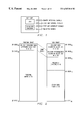
- FIG. 1 illustrates a high-level block diagram of a DSP core of the present invention
- FIG. 2 shows a high-level memory map for the DSP core of FIG. 1;
- FIGS. 3A, 3 B and 3 C show possible maps for a portion of FIG. 2;
- FIGS. 4A, 4 B and 4 C show possible maps for a portion of FIG. 2;
- FIG. 5 is a block diagram of a CPU of FIG. 1;
- FIG. 6 illustrates individually accessible portions of the accumulator of the CPU of FIG. 5;
- FIG. 7 illustrates individually accessible halves of the P Register of the CPU of FIG. 5;
- FIG. 8 illustrates pages of Data Memory
- FIG. 9 shows Address Reach of the Stack Pointer
- FIG. 10 shows Address Reach of the Auxiliary Registers
- FIG. 11 AR 6 and AR 7 ;
- FIG. 12 shows the bit positions of Status Register ST 0 ;
- FIG. 13 shows the bit positions of Status Register ST 1 ;
- FIG. 14 shows Status Register ST 0 ;
- FIG. 15 shows Status Register ST 1 ;
- FIG. 16 illustrates a block Diagram of Components Involved in the multiplier of the CPU of FIG. 5;
- FIG. 17 illustrates the symbols and their meanings for the Shift Operations depicted in FIGS. 18;
- FIGS. 18A, 18 B and 18 C show Shift Operations
- FIG. 19 illustrates the bit positions for an Interrupt Flag Register (IFR);
- FIG. 20 illustrates the bit positions for an Interrupt Enable Register (IER);
- FIG. 21 illustrates the bit positions for a Debug Interrupt Enable Register (DBGIER);
- FIG. 22 illustrates a Process for Maskable Interrupts
- FIG. 23 illustrates a Functional Flow Chart for an Interrupt Initiated by a TRAP Instruction
- FIGS. 24A and 24B illustrate pipeline phases and relationships between Address Counters FC, IC and PC;
- FIG. 25 illustrates pipeline Phases During Which Address Registers Are Read From or Written To
- FIG. 26 shows an Accessing Memory in Immediate-Pointer Addressing Mode
- FIG. 27 illustrates Pages of Data Memory
- FIG. 28 illustrates Accessing Data Memory in Stack-Pointer Indirect Addressing Mode
- FIG. 29 illustrates Accessing Data Memory in PAGE 0 Stack Addressing Mode
- FIG. 30 illustrates Accessing Data Memory with the Auxiliary Registers
- FIG. 31 shows a Circular Addressing Mode
- FIG. 32 illustrates Opcode Addressing Mode Information
- FIG. 33 shows an Opcode Format for Immediate Addressing With an 8-Bit Constant
- FIG. 34 shows an Opcode Format for Immediate Addressing With a 5-Bit Constant
- FIG. 35 shows an Opcode Format for Immediate Addressing With a 16-Bit Constant
- FIG. 36 shows an Opcode Format for Immediate Addressing With a 22-Bit Constant
- FIG. 37 shows an Opcode Format for an Instruction Using Register Addressing Mode
- FIG. 38 shows an Opcode Format for an Instruction Using DP Direct Addressing Mode
- FIG. 39 shows an Opcode Format for an Instruction Using Auxiliary-Register Indirect Addressing Mode
- FIG. 40 shows an Opcode Format for an Instruction Using Stack-Pointer Indirect Addressing Mode
- FIG. 41 illustrates a 32-Bit Read From Data Memory
- FIG. 42 illustrates a 32-Bit Write to Data Memory
- FIG. 43 illustrates an example Opcode taken from the Assembly Language Instructions.
- a digital signal processor (DSP) chip contains a DSP core.
- the DSP core is responsible for the central control activities of a DSP, activities such as address generation, arithmetic operations, data transfers, and system monitoring.
- activities such as address generation, arithmetic operations, data transfers, and system monitoring.
- the DSP core of the present invention is a 16-bit, fixed-point processor. As shown in FIG. 1, this DSP core contains:
- a CPU for: generating data- and program-memory addresses, decoding and executing instructions, performing arithmetic, logical, and shift operations, and controlling data transfers among CPU registers, data memory, and program memory;
- c) signals for: interfacing with memory and peripherals, clocking and controlling the CPU and the emulation circuitry, showing the status of the CPU and the emulation circuitry, and using interrupts.
- the DSP core does not contain memory, a clock generator, or peripheral devices.
- a protected pipeline The CPU implements an 8-phase pipeline that prevents a read from and a write to the same location from occurring out of order;
- the CPU contains registers that are not mapped to data space. These registers function as system-control registers, math registers, and data pointers. The system-control registers are accessed by special instructions. The other registers are accessed by special instructions or by a special addressing mode (register addressing mode);
- ALU arithmetic logic unit
- ARAU address register arithmetic unit
- barrel shifter This shifter performs all left and right shifts of data. It can shift data to the left by up to 16 bits and to the right by up to 16 bits;
- multiplier performs 16-bit ⁇ 16-bit 2s-complement multiplication with a 32-bit result.
- the multiplication can be performed with two signed numbers, two unsigned numbers, or one signed number and one unsigned number.
- the emulation logic includes the following features:
- debug and test direct memory access (DT-DMA)—The debug host can gain direct access to the content of registers and memory by taking control of the memory interface during unused cycles of the instruction pipeline;
- a debug event When a debug event causes the DSP to enter the debug state, the event is called a break event.
- the DSP core has four main types of signals:
- memory-interface signals These signals transfer data among the core, memory, and peripherals; indicate program-memory accesses and data-memory accesses; and differentiate between accesses of different sizes (16-bit or 32-bit).
- clock and control signals These signals provide clocking for the CPU and the emulation logic, and they are used to control and monitor the CPU.
- reset and interrupt signals These signals are used for generating a hardware re-set and interrupts, and for monitoring the status of interrupts.
- the DSP core contains no memory, but can access memory elsewhere on-chip with the DSP or off chip.
- FIG. 2 shows a high-level memory map view of how addresses may be allocated between program space and data space.
- hexadecimal numbers are shown with a subscript of 16.
- the hexadecimal number 40 would be shown as 40 16 .
- the exception to this rule is a hexadecimal number in a code example; these hexadecimal numbers have the suffix h.
- the number 40 in the following code is a hexadecimal 40.
- the memory map in FIG. 2 has been divided into the following segments:
- Addresses 000800 16 -000CFF 16 in data space are reserved for special registers. Some of the addresses in the range 000800 16 -0009FF 16 are used for accessing memory-mapped emulation registers.
- Additional data memory may be on-chip and/or off-chip.
- VMAP Sixty-four addresses in program space are set aside for a table of 32 interrupt vectors.
- BO may be selected as 256, 512, or 1K words, as depicted in FIGS. 3A, 3 B, and 3 C, respectively. If B 0 has fewer than 1024 (1K) words, some of the program/data addresses are reserved (not available for use).
- the 1K block of memory shown in FIGS. 3A-C can be addresses in program space or data space.
- the location with address 00 0041 16 may be in program space or in data space.
- FIGS. 4A-C show the possible maps for block B 1 , which reside only in data space.
- B 1 may be selected to be 256, 512, or 1K words, as depicted in FIGS. 4A, 4 B, and 4 C, respectively. If B 1 has 256 words, mirrors of B 1 are in the address ranges 00 01000 16 -00 01FF 16 , 00 0200 16 -00 02FF 16, and 00 0300 16 -00 03FF 16 As an example of what this means, the first word of B 1 , may be accessed at any one of the following addresses: 00 0000 16 , 00 0100 16 , 00 0200 16 , or 00 0300 16 .
- B 1 has 512 words, there is one mirror of B 1 at addresses 00 0200 16 -00 0400 16 . If B 1 has 1K words, it uses all the available addresses.
- the DSP CPU supports long call and branch operations, and a 22-bit program counter (PC) enables access of program space as one linear memory space.
- PC program counter
- the DSP also supports relative offset branching, which enables code to be relocated at run time.
- the DSP CPU supports a 16-bit stack pointer (SP) that points to data memory. Using this register, a stack may be created within the first 64K of data space (addresses 00 0000 16 -00 FFFF 16 ). SP is incremented such that the stack grows from low memory to high memory and SP always points to the next empty location. After a hardware reset, SP points to address 00 0000 16 .
- SP stack pointer
- Indirect addressing modes use 16-bit pointers (the SP and the auxiliary registers AR 0 -AR 5 ) to access the low 64K of data space and 22-bit pointers (auxiliary registers XAR 6 and XAR 7 ) to access the full range of data space.
- Direct addressing modes access all of data space by concatenating a 16-bit data page number with a 6-bit offset that is embedded in an instruction. The addressing modes are described later herein.
- the PREAD instruction can be used to transfer a program-memory value to data memory.
- the PWRITE instruction can transfer a data-memory value to program memory.
- the DSP memory map is accessible outside the core by the memory interface, which connects the DSP core to memories, peripherals, or other interfaces.
- the memory interface includes separate buses for program space and data space. This means an instruction can be fetched from program memory while data memory is being accessed.
- the interface also includes signals that indicate the type of read or write being requested by the CPU. These signals can select a specified memory block or peripheral for a given bus transaction.
- the DSP supports special byte-access instructions which can access the least significant byte (LSByte) or most significant byte (MSByte) of an addressed 16-bit word. Strobe signals indicate when such an access is occurring on a data bus.
- the memory interface has three 22-bit address buses:
- PAB program address bus
- the data-read address bus (DRAB) carries addresses for reads from data space
- the data-write address bus (DWAB) carries addresses for writes to data space.
- the memory interface also has three 32-bit data buses:
- PRDB program-read data bus
- DRDB data-read data bus
- the data-/program-write data bus (DWDB) carries data during writes to data space or program space.
- a program-space read and a program-space write cannot happen simultaneously because both use the PAB.
- a program-space write and a data-space write cannot happen simultaneously because both use the DWDB.
- the CPU can read from program space (using PAB and PRDB), read from data space (using DRAB and DRDB), and write to data space (using DWAB and DWDB) at the same time.
- PAB and PRDB are used only for reading instructions from program space
- DWDB is used only for writing data to data space.
- Table 2 the instructions in Table 2 below are exceptions to this behavior.
- this instruction multiplies two data values, one of which is read from program space.
- the core places the program-space source address on the program address bus (PAB), sets the appropriate program-space select signals, and reads the program data value from the program read data bus (PRDB).
- PAB program address bus
- PRDB program read data bus
- the DSP core expects memory wrappers or peripheral-interface logic to align any 32-bit read or write to an even address. If the address-generation logic generates an odd address, the CPU must begin reading or writing at the previous even address. This alignment does not affect the address values generated by the address-generation logic.
- the central processing unit is responsible for controlling the flow of a program and the processing of instructions. It performs arithmetic, Boolean-logic, multiply, and shift operations.
- FIG. 5 shows the major blocks and data paths of the CPU of the DSP core of the present invention.
- the shaded buses are memory-interface buses that are external to the CPU.
- the main blocks of the CPU are:
- program control logic This logic stores a queue of instructions that have been fetched from program memory by way of the program-read bus (PRDB). It also decodes these instructions and passes commands and constant data to other parts of the CPU.
- PRDB program-read bus
- program address generation logic This logic generates the addresses used to fetch instructions or data from program memory and places each address on the program address bus, (PAB). As part of its operation, the program-address generation logic uses several counters, addresses supplied by the program control logic, and addresses from the extended auxiliary register XAR 7 .
- ARAU address register arithmetic unit
- the ARAU generates addresses for values that must be fetched from data memory. For a data read, it places the address on the data-read address bus (DRAB); for a data write, it loads the data-write address bus (DWAB).
- DRAB data-read address bus
- DWAB data-write address bus
- the ARAU also increments or decrements the stack pointer (SP) and the auxiliary registers (AR 0 , AR 1 , AR 2 , AR 3 , AR 4 , AR 5 , XAR 6 , and XAR 7 ).
- ALU arithmetic logic unit
- the 32-bit ALU performs 2s-complement arithmetic and Boolean logic operations. Before doing its calculations, the ALU accepts data from registers, from data memory, or from the program control logic. Inputs come from the registers, the program control logic, and the data-read data bus (DRDB). Results that go to data memory are sent to the data-/program-write data bus (DWDB).
- ALU arithmetic logic unit
- multiplier performs 16-bit ⁇ 16-bit 2s-complement multiplication with a 32-bit result.
- the DSP uses the 16-bit multiplicand register (T), the 32-bit product register (P), and the 32-bit accumulator (ACC).
- T register supplies one of the values to be multiplied.
- the result of the multiplication can be sent to the P register or to ACC.
- barrel shifter performs all the shifts for the DSP. It can shift data to the left by up to 16 bits and to the right by up to 16 bits. The amount and direction of the shift is determined by the particular instruction that causes the shift.
- Table 3 lists the main CPU registers and their values after reset. The registers are described in more detail later herein.
- the VMAP bit is bit 3 of ST1.
- the PC will be loaded with the reset vector at either address 00_0000 16 or address 3F_FFC0 16. ⁇ The value in ST1 after reset depends, in part, on the level on the VMAP input signal at the time reset is initiated. If the VMAP signal is low, bit 3 (VMAP) is cleared. If the VMAP signal is high bit 3 is set.
- the accumulator is the main working register for the CPU. It is the destination for all ALU operations except those which operate directly on memory and registers. ACC supports single-cycle move, add, subtract, and compare operations from 32-bit-wide data memory. It can also accept the 32-bit result of a multiplication operation. As depicted in FIG. 6, the halves and quarters of the ACC can also be individually accessed. ACC can be treated as two independent 16-bit registers: AH (high 16 bits) and AL (low 16 bits). The bytes within AH and AL can also be accessed independently. Special byte-move instructions load and store the most significant byte or least significant byte of AH or AL. This enables efficient byte packing and unpacking.
- the accumulator has the following associated status bits. The details on these bits are described later herein with reference to a status register, ST 0 .
- Overflow mode bit (OVM), Sign-extension mode bit (SXM), Test/control flag bit (TC), Carry bit (C), Zero flag bit (Z), Negative flag bit (N), Latched overflow flag bit (V), Overflow counter bits (OVC).
- Table 4 below shows the ways to shift the content of AH, AL, or ACC.
- the multiplicand register (T register) is primarily used to store a 16-bit signed integer value prior to a multiply operation. During every multiplication, one of the multiplicands is taken from the T register. For some left and right barrel-shift operations, the shift amount (0 to 15) is determined by the four least significant bits of the T register. In these shift operations, the 12 most significant bits of T are ignored. The contents of T can be stored back to memory.
- the product register (P register) (P/PH, PL) is typically used to hold the 32-bit result of a 16 ⁇ 16 multiplication. It can also be loaded directly from a 16- or 32-bit data-memory location, a 16-bit constant, the 32-bit ACC, or a 16-bit addressable CPU register. As shown in FIG. 7, the P register may be treated as a 32-bit register or as two independent 16-bit registers: PH (high 16 bits) and PL (low 16 bits).
- data memory In the direct addressing modes, data memory is addressed in blocks of 64 words called data pages. The entire 4M words of data memory consists of 65 536 data pages labeled 0 through 65 535 , as shown in FIG. 8 .
- DP direct addressing mode the 16-bit data page pointer (DP) holds the current data page number. The data page is changed by loading the DP with a new number.
- the stack pointer enables the use of a software stack in data memory. As depicted in FIG. 9, the stack pointer has only 16 bits and can only address the low 64K of data space. When the SP is used, the upper six bits of the 22-bit address are forced to 0. (For information about addressing modes that use the SP). After reset, SP points to address 00 0000 16 .
- the operation of the stack is as follows: the stack grows from low memory to high memory; the SP always points to the next empty location in the stack; at reset, the SP is cleared, so that it points to address 000000 16 .
- the DSP core When 32-bit operations read or write a 32-bit value, the DSP core expects the memory wrapper or peripheral-interface logic to align that read or write to an even address. For example, if the SP contains the odd address 000083 16 , a 32-bit read operation reads from addresses 000082 16 and 000083 16 .
- the SP will overflow if its value is increased beyond FFFF 16 or decreased below 0000 16 .
- the SP increases past FFFF 16 , it counts forward from 0000 16 .
- the result is 000 16 .
- the SP decreases past 0000 16 , it counts backward from FFFF 16 .
- the SP When values are being saved to the stack, the SP is not forced to align with even or odd addresses. Alignment is forced by the memory wrapper or peripheral-interface logic.
- the CPU provides eight auxiliary registers that can be used as pointers to memory. There are six 16-bit auxiliary registers (AR 0 , AR 1 , AR 2 , AR 3 , AR 4 , and AR 5 ), and two 22-bit extended auxiliary registers (XAR 6 and XAR 7 ).
- FIG. 10 shows the ranges of data memory accessible to the 16-bit and 22-bit auxiliary registers. Because AR 0 -AR 5 are 16-bits wide, their range is limited to addresses 00 0000 16 -00 FFFF 16 . When one of these six auxiliary registers is used, the content of the auxiliary register (or the content plus an offset) is concatenated with six leading zeros to form the full 22-bit address.
- XAR 6 and XAR 7 being 22 bits wide, can be used to access the full range of data memory. XAR 7 can also be used by some instructions to point to any value in program memory.
- auxiliary register AR 6 the 16 least significant bits of XAR 6 and XAR 7 .
- auxiliary register AR 7 the 16 least significant bits of XAR 6 and XAR 7 .
- the 22-bit program counter (PC) always points to the instruction that is currently being processed—the instruction that has just reached the decode 2 phase of the pipeline. Once an instruction reaches this phase of the pipeline, it cannot be flushed from the pipeline by an interrupt. It is executed before the interrupt is taken.
- the DSP has two status registers, ST 0 and ST 1 , which contain various flag bits and control bits. These registers can be stored into and loaded from data memory, enabling the status of the machine to be saved and restored for sub-routines.
- FIG. 12 and FIG. 13 show the organization of status registers ST 0 and ST 1 , respectively. The status bits have been organized according to when the bit value is modified in the pipeline. Bits in ST 0 are modified in the execute phase of the pipeline; bits in ST 1 are modified in the decode 2 phase. The status bits are described in detail later herein.
- R means a Read access and W means a Write access; the value following dash ( ⁇ ) is value after reset. Reserved bits are always 0s and are not affected by writes.
- the value of the VMAP bit after reset depends on the level of the VMAP input signal at reset. If the VMAP signal is low, the VMAP bit is 0 after reset; if the VMAP signal is high, the VMAP bit is 1 after reset.
- the DSP has three registers dedicated to the control of interrupts: interrupt flag register (IFR); interrupt enable register (IER); and debug interrupt enable register (DBGIER).
- IFR interrupt flag register
- IER interrupt enable register
- DSGIER debug interrupt enable register
- the IFR contains flag bits for maskable interrupts (those that can be enabled and disabled with software). When one of these flags is set, by hardware or software, the corresponding interrupt will be serviced if it is enabled. A maskable interrupt is enabled or disabled by its corresponding bit in the IER.
- the DBGIER indicates the time-critical interrupts that will be serviced (if enabled) while the DSP is in real-time emulation mode and the CPU is halted. The DSP interrupts and the interrupt-control registers are described later herein.
- FIG. 14 shows the bit fields of status register ST 0 . All of these bit fields are modified in the execute phase of the pipeline. Detailed descriptions of these bits follow the figure.
- R means a Read access and W means a Write access; the value following dash ( ⁇ ) is value after reset.
- bits 15 - 10 are the overflow counter (OVC).
- the overflow counter is a 6-bit signed counter with a range of ⁇ 32 to 31.
- OVC overflow counter
- OVC overflow counter
- the OVC When ACC overflows in the positive direction (from 7FFFF FFFF 16 to 8000 0000 16 ) the OVC is incremented by 1. When ACC overflows in the negative direction (from 8000 0000 16 to 7FFF FFFF 16 ) the OVC is decremented by 1. The increment or decrement is performed as the overflow affects the V flag.
- OVC is not affected by overflows in registers other than ACC and is not affected by compare instructions (CMP and CMPL). Table 6 below, explains how OVC may be affected by the saturate accumulator (SAT ACC) instruction.
- bits 9 - 7 are product shift mode bits (PM). This 3-bit value determines the shift mode for any output operation from the product (P) register.
- the shift modes are shown in Table 7. The output can be to the ALU or to memory. All instructions that are affected by the product shift mode will sign extend the P register value during a right shift operation. At reset, PM is cleared.
- An overflow occurs in ACC (and V is set) if the result of an addition or subtraction does not fit within the signed numerical range ⁇ 2 31 to (+2 31 ⁇ 1), or 800 000 16 to 7FFF FFFF 16 .
- An overflow occurs in AH, AL, or another 16-bit register or data-memory location if the result of an addition or subtraction does not fit within the signed numerical range ⁇ 2 15 to (+2 15 ⁇ 1), or 8000 16 to 7FFF 16 .
- bit 5 is the negative flag (N). During certain operations, N is set if the result of the operation is a negative number or cleared if the result is a positive number. At reset, N is cleared. Results in ACC are tested for the negative condition. Bit 31 of ACC is the sign bit. If bit 31 is a 0, ACC is positive; if bit 31 is a 1, ACC is negative. N is set if a result in ACC is negative or cleared if a result is positive.
- results in AH, AL, and other 16-bit registers or data-memory locations are also tested for the negative condition.
- bit 15 of the value is the sign bit (1 indicates negative, 0 indicates positive).
- N is set if the value is negative or cleared if the value is positive.
- the TEST ACC instruction sets N if the value in ACC is negative. Otherwise the instruction clears N.
- the N flag is set differently under overflow conditions than for addition or subtraction operations.
- the N flag is set to match the most significant bit of the truncated result.
- the N flag assumes infinite precision. This applies to operations whose result is loaded to ACC, AH, AL, another register, or a data-memory location.
- N Condition N Condition 0 The tested number is positive, or N has been cleared. 1 The tested number is negative, or N has been cleared
- bit 4 is the zero flag (Z).
- Z is set if the result of certain operations is 0 or is cleared if the result is nonzero. This applies to results that are loaded into ACC, AH, AL, another register, or a data-memory location. At reset, Z is cleared. The TEST ACC instruction sets Z if the value in ACC is 0. Otherwise, it clears Z. Z can be summarized as follows:
- bit 3 is the carry bit (C). This bit indicates when an addition or increment generates a carry or when a subtraction, compare, or decrement generates a borrow. It is also affected by rotate operations on ACC and barrel shifts on ACC, AH, and AL. During additions/increments, C is set if the addition generates a carry; otherwise C is cleared. There is one exception: when using the ADD instruction with a shift of 16, the ADD instruction can set C but cannot clear C.
- C is cleared if the subtraction generates a carry; otherwise C is set. There is one exception: when using the SUB instruction with a shift of 16, the SUB instruction can clear C but can-not set C. This bit can be individually set and cleared by the SETC C instruction and CLRC C instruction, respectively. At reset, C is cleared.
- C can be summarized as follows:
- bit 2 is the test/control flag (TC). This bit shows the result of a test performed by either the TBIT (test bit) instruction or the NORM (normalize) instruction.
- the TBIT instruction tests a specified bit.
- TBIT test bit
- the TC bit is set if the tested bit is 1 or cleared if the tested bit is 0.
- NORM When a NORM instruction is executed, TC is modified as follows: If ACC holds 0, TC is set. If ACC does not hold 0, the CPU calculates the exclusive- OR of ACC bits 31 and 30 , and then loads TC with the result. This bit can be individually set and cleared by the SETC TC instruction and CLRC TC instruction, respectively. At reset, TC is cleared.
- bit 1 is the overflow mode bit (OVM).
- OVM overflow mode bit
- ACC is filled with either its most positive or most negative value as follows: If ACC overflows in the positive direction (from 7FFF FFFF 16 to 8000 0000 16 ), ACC is then filled with 7FFF FFFF 16 . If ACC overflows in the negative direction (from 8000 0000 16 to 7FFF FFFF 16 ), ACC is then filled with 8000 0000 16 .
- This bit can be individually set and cleared by the SETC OVM instruction and CLRC OVM instruction, respectively. At reset, OVM is cleared.
- bit 0 is the sign-extension mode bit (SXM).
- SXM sign-extension mode bit
- SXM affects the ADD, SUB, and MOV instructions that shift a 16-bit value before using it in an operation on the 32-bit ACC.
- SXM also determines whether ACC is sign extended when it is shifted right by the SFR instruction.
- SXM does not affect instructions that shift the product register value; all right shifts of the product register value use sign extension. This bit can be individually set and cleared by the SETC SXM instruction and CLRC SXM instruction, respectively. At reset, SXM is cleared.
- FIG. 15 shows the bit fields of status register ST 1 . All of these bit fields are modified in the decode 2 phase of the pipeline. Detailed descriptions of these bits are provided later herein.
- the value of the VMAP bit after reset depends on the level of the VMAP input signal at reset. If the VMAP signal is low, the VMAP bit is 0 after reset; if the VMAP signal is high, the VMAP bit is 1 after reset.
- bits 15 - 13 are the auxiliary register pointer (ARP).
- ARP auxiliary register pointer
- This 3-bit field points to the current auxiliary register. This could be one of the 16-bit auxiliary registers (AR 0 to AR 5 ) or one of the 22-bit extended auxiliary registers (XAR 6 or XAR 7 ).
- the mapping of ARP values to auxiliary registers is as follows:
- bits 12 - 8 are reserved and writes to these bits have no effect.
- bit 7 is the IDLE status bit (IDLESTAT). This read-only bit is set when the IDLE instruction is executed. It is cleared by any one of the following events: an interrupt is serviced; an interrupt is not serviced but takes the core out of the IDLE state; a valid instruction enters the instruction register (the register that holds the instruction currently being decoded); and a device reset occurs.
- IDLE status bit IDLESTAT
- IDLESTAT When the CPU services an interrupt, the current value of IDLESTAT is saved on the stack (when ST 1 is saved on the stack), and then IDLESTAT is cleared. Upon return from the interrupt, IDLESTAT is not restored from the stack.
- bit 6 is the emulation access enable bit (EALLOW). This bit, when set, enables access to emulation registers. EALLOW is set by the EALLOW instruction and cleared by the EDIS instruction. EALLOW is written to by using the POP ST 1 instruction or the POP DP:ST 1 instruction. When the CPU services an interrupt, the current value of EALLOW is saved on the stack (when ST 1 is saved on the stack), and then EALLOW is cleared. Therefore, at the start of an interrupt service routine (ISR), access to emulation registers is disabled. If the ISR must access emulation registers, it must include an EALLOW instruction. At the end of the ISR, EALLOW can be restored by the IRET instruction.
- ISR interrupt service routine
- bit 5 is the Loop instruction status bit (LOOP).
- LOOP is set when a loop instruction (LOOPNZ or LOOPZ) reaches the decode 2 phase of the pipeline. The loop instruction does not end until a specified condition is met. When the condition is met, LOOP is cleared. LOOP is a read-only bit; it is not affected by any instruction except a loop instruction.
- the CPU services an interrupt, the current value of LOOP is saved on the stack (when ST 1 is saved on the stack), and then LOOP is cleared. Upon return from the interrupt, LOOP is not restored from the stack.
- bit 4 is the Stack pointer alignment bit (SPA). SPA indicates whether the CPU has previously aligned the stack pointer to an even address:
- bit 3 is the Vector map bit (VMAP). VMAP determines whether the interrupt vectors (including the reset vector) are mapped to the lowest or highest addresses in program memory:
- VMAP Condition 0 Interrupt vectors are mapped to the bottom of program memory, addresses 000000 16 - 00003F 16 .
- 1 Interrupt vectors are mapped to the top of program memory, addresses 3FFFC0 16 - 3FFFFF 16 .
- the core input signal VMAP is sampled on reset. If the signal is high, the VMAP bit is set. If the signal is low, the VMAP bit is cleared.
- the output core signal VMAPS reflects the status of the VMAP bit. This bit can be individually set and cleared by the SETC VMAP instruction and CLRC VMAP instruction, respectively.
- bit 2 is the PAGE 0 addressing modes configuration bit (PAGE 0 ).
- PAGE 0 selects between two mutually-exclusive addressing modes: PAGE 0 direct addressing mode and PAGE 0 stack addressing mode. Selection of the modes is as follows:
- This bit can be individually set and cleared by the SETC PAGE 0 instruction and CLRC PAGE 0 instruction, respectively. At reset, the PAGE 0 bit is cleared (PAGE 0 stack addressing mode is selected).
- bit 1 is the Debug enable mask bit (DBGM).
- DBGM is primarily used in emulation to block debug events in time-critical portions of program code. DBGM enables or disables debug events as follows:
- DBGM When the CPU services an interrupt, the current value of DBGM is saved on the stack (when ST 1 is saved on the stack), and then DBGM is set. Upon return from the interrupt, DBGM is restored from the stack. This bit can be individually set and cleared by the SETC DBGM instruction and CLRC DBGM instruction, respectively. DBGM is also set automatically during interrupt operations. At reset, DBGM is set. Executing the ABORTI (abort interrupt) instruction also sets DBGM.
- bit 0 is the Interrupt global mask bit (NTM). This bit globally enables or disables all maskable interrupts (those that can be blocked by software):
- Maskable interrupts are globally enabled. In order to be acknowledged by the CPU, a maskable interrupt must also be locally enabled by the interrupt enable register (IER). 1 Maskable interrupts are globally disabled. Even if a maskable interrupt is locally enabled by the interrupt enable register (IER), it is not acknowledged by the CPU.
- IER interrupt enable register
- INTM has no effect on the nonmaskable interrupts, including a hardware re-set or the hardware interrupt NMI.
- the state of INTM is saved/restored whenever status register ST 1 is pushed to/popped from the stack.
- the current value of INTM is saved on the stack (when ST 1 is saved on the stack), and then INTM is set.
- INTM is restored from the stack. This bit can be individually set and cleared by the SETC INTM instruction and CLRC INTM instruction, respectively.
- INTM is set.
- the value in INTM does not cause modification to the interrupt flag register (IFR), the interrupt enable register (IER), or the debug interrupt enable register (DBGIER).
- IFR interrupt flag register
- IER interrupt enable register
- DBGIER debug interrupt enable register
- the program control logic and program-address generation logic work together to provide proper program flow.
- the flow of a program is sequential: the CPU executes instructions at consecutive program-memory addresses. At times, a discontinuity is required; that is, a program must branch to a non-sequential address and then execute instructions sequentially at that new location.
- the DSP supports interrupts, branches, calls, returns, and repeats. Proper program flow also requires smooth flow at the instruction level. To meet this need, the DSP supports a fully protected pipeline and an instruction-fetch mechanism that attempts to keep the pipeline full.
- Interrupts are hardware- or software-driven events that cause the CPU to suspend its current program sequence and execute a subroutine called an interrupt service routine. Interrupts are described in detail later herein.
- Branch instructions B, SB, and BANZ are conditional. They are executed only if a certain specified or predefined condition is met.
- the repeat (RPT) instruction allows the execution of a single instruction (N +1) times, where N is specified as an operand of the RPT instruction.
- the instruction is executed once and then repeated N times.
- the repeat counter (RPTC) is loaded with N. RPTC is then decremented every time the repeated instruction is executed, until RPTC equals 0.
- Each instruction passes through eight independent phases that form an instruction pipeline. At any given time, up to eight instructions may be active, each in a different phase of completion. Not all reads and writes happen in the same phases, but a pipeline-protection mechanism stalls instructions as needed to ensure that reads and writes to the same location happen in the order in which they are programmed.
- an instruction-fetch mechanism attempts to keep the pipeline full. Its role is to fill an instruction-fetch queue, which holds instructions in preparation for decoding and execution.
- the instruction-fetch mechanism fetches 32-bits at a time from program memory; it fetches one 32-bit instruction or two 16-bit instructions.
- the instruction-fetch mechanism uses three program-address counters: the program counter (PC), the instruction counter (IC), and the fetch counter (FC).
- PC program counter
- IC instruction counter
- FC fetch counter
- the DSP has a 16-bit ⁇ 16-bit hardware multiplier that can produce a 32-bit signed or unsigned 32-bit product.
- FIG. 16 shows the CPU components involved in multiplication.
- the multiplier accepts two 16-bit inputs:
- T 16-bit multiplicand register
- Most DSP multiply instructions require loading T from a data-memory location or a register before executing the instruction.
- the MAC instruction, one syntax of the MPY instruction, and one syntax of the MPYA instruction also load T before the multiplication.
- the 32-bit result is stored in one of two places, depending on the particular multiply instruction: the 32-bit product register (P) or the 32-bit accumulator (ACC).
- the shifter holds 32 bits and accepts either a 16-bit or 32-bit input value.
- the value is loaded into the 16 least significant bits (LSBs) of the shifter.
- the output of the shifter may be all of its 32 bits or just its 16 LSBs.
- N When a value is shifted right by an amount N, the N LSBs of the value are lost and the bits to the left of the value are filled with all 0s or all 1s. If sign extension is specified, the bits to the left are filled with copies of the sign bit. If sign extension is not specified, the bits to the left are filled with 0s, or zero filled.
- the bits to the right of the shifted value are zero filled. If the value has 16 bits and sign extension is specified, the bits to the left are filled with copies of the sign bit. If the value has 16 bits and sign extension is not specified, the bits to the left are zero filled. If the value has 32 bits, the N most significant bits (MSBs) of the value are lost, and sign extension is irrelevant.
- MSBs most significant bits
- FIGS. 18A-18C list the instructions that use the shifter, provides an illustration of the corresponding shifter operation and uses the graphical symbols depicted in FIG. 17 .
- Interrupts are hardware- or software-driven signals that cause the DSP to suspend its current program sequence and execute a subroutine.
- interrupts are generated by hardware devices that need to give data to or take data from the DSP (for example, A/D and D/A converters and other processors).
- Interrupts can also signal that a particular event has taken place (for example, a timer has finished counting).
- interrupts can be triggered by software (the INTR, OR IFR, or TRAP instruction) or by hardware (a pin, a peripheral, or on-chip logic). If hardware interrupts are triggered at the same time, the DSP services them according to a set priority ranking.
- software the INTR, OR IFR, or TRAP instruction
- hardware a pin, a peripheral, or on-chip logic
- Maskable interrupts These are interrupts that can be blocked (masked) or enabled (unmasked) through software.
- Nonmaskable interrupts These interrupts cannot be blocked. The DSP will immediately approve this type of interrupt and branch to the corresponding subroutine. All software-initiated interrupts are in this category.
- the DSP handles interrupts in four main phases:
- the DSP branches to its corresponding subroutine called an interrupt service routine (ISR).
- ISR interrupt service routine
- the DSP branches to the address (vector) stored at a predetermined vector location and executes the ISR.
- the DSP supports 32 interrupt vectors, including the reset vector.
- Each vector is a 22-bit address that is the start address for the corresponding interrupt service routine (ISR).
- ISR interrupt service routine
- Each vector is stored in 32 bits at two consecutive addresses. The lower address holds the 16 least significant bits (LSBs) of the vector. The higher address holds the 6 most significant bits (MSB) right-justified.
- LSBs least significant bits
- MSB most significant bits
- Table 21 lists the available interrupt vectors and their locations. The addresses are shown in hexadecimal form. The table also shows the priority of each of the hardware interrupts.
- the vector table can be mapped to the top or bottom of program space, depending on the value of the vector map bit (VMAP) in status register ST 1 . If the VMAP bit is 0, the vectors are mapped beginning at address 000000 16 . If the VMAP bit is 1, the vectors are mapped beginning at address 3FFFCO 16 . Table 21 lists both address offsets and absolute addresses.
- the VMAP bit can be set by the SETC VMAP instruction and cleared by the CLRC VMAP instruction.
- the input core signal VMAP sampled only at reset, determines the reset value of the VMAP bit.
- the state of the VMAP bit is also reflected at the output core signal VMAPS.
- ⁇ overscore (INT 1 ) ⁇ - ⁇ overscore (IN 14 ) ⁇ are 14 general-purpose interrupts.
- DLOGINT the data log interrupt
- RTOSINT the real-time operating system interrupt
- IFR interrupt flag register
- IER interrupt enable register
- DSGIER debug interrupt enable register
- the 16-bit interrupt flag register contains flag bits that indicate which of the corresponding interrupts are pending (waiting approval from the CPU).
- the external input lines ⁇ overscore (INT 1 ) ⁇ - ⁇ overscore (IN 4 ) ⁇ are sampled at every CPU clock cycle. If an active interrupt is recognized, the corresponding bit in the IFR is set and latched.
- a signal sent by the core's on-chip analysis logic causes the corresponding flag bits to be set and latched.
- One or more of the IFR bits may be set at the same time by using the OR IFR instruction.
- the interrupt enable register (IER) and the debug interrupt enable register (DBGIER) each contain bits for individually enabling or disabling ⁇ overscore (INT 1 ) ⁇ - ⁇ overscore (IN 14 ) ⁇ , DLOGINT, and RTOSINT.
- IER interrupt enable register
- DBGIER debug interrupt enable register
- the DBGIER indicates which interrupts may be serviced when the core is in the real-time emulation mode. The IER and the DBGIER are discussed later herein.
- ⁇ overscore (INT 1 ) ⁇ - ⁇ overscore (IN 14 ) ⁇ , DLOGINT, and RTOSINT also share bit 0 in status register ST 1 .
- the corresponding interrupt will not be serviced until it is appropriately enabled by two of the following: the IER, the DBGIER, and the INTM bit.
- the requirements for enabling ⁇ overscore (INT 1 ) ⁇ - ⁇ overscore (IN 14 ) ⁇ , DLOGINT, and RTOSINT depend on the interrupt-handling process used. In the standard process, which occurs in most circumstances, the DBGIER is ignored. When the DSP is in real-time emulation mode and the CPU is halted, a different process is used. In this special case, the DBGIER is used and the INTM bit is ignored. (If the DSP is in real-time mode and the CPU is running, the standard interrupt-handling process applies.) Once an interrupt has been requested and properly enabled, the CPU prepares for and then executes the corresponding interrupt service routine.
- FIG. 19 shows the Interrupt Flag Register (IFR).
- IFR Interrupt Flag Register
- Bits 15 and 14 of the IFR correspond to the interrupts RTOSINT and DLOGINT:
- RTOSINT 0 RTOSINT is not pending.
- RTOSINT 1 RTOSINT is pending.
- bits INT 1 -INT 14 the following general description applies:
- FIG. 20 shows the Interrupt Enable Register (IER).
- IER Interrupt Enable Register
- To enable an interrupt set its corresponding bit to 1.
- To disable an interrupt clear its corresponding bit to 0.
- Two syntaxes of the MOV instruction allow reading from the IER and writing to the IER.
- the OR IER instruction enables setting IER bits
- the AND IER instruction enables clearing IER bits.
- the corresponding IER bit is cleared.
- all the IER bits are cleared to 0, disabling all the corresponding interrupts.
- the TRAP instruction if the corresponding IER bit is set, the CPU does not clear it automatically. If an application requires that the IER bit be cleared, the bit must be cleared in the interrupt service routine.
- R means a Read access and W means a Write access; the value following dash ( ⁇ ) is value after reset.
- Bits 15 and 14 of the IER enable or disable the interrupts RTOSINT and DLOGINT:
- RTOSINT 0 RTOSINT is disabled.
- RTOSINT 1 RTOSINT is enabled.
- bits INT 1 -INT 14 the following general description applies:
- FIG. 21 shows the Debug Interrupt Enable Register (DBGIER), which is only used when the CPU is halted in real-time emulation mode.
- DBGIER Debug Interrupt Enable Register
- An interrupt enabled in the DBGIER is defined as a time-critical interrupt.
- the only interrupts that are serviced are time-critical interrupts that are also enabled in the IER. If the CPU is running in real-time emulation mode, the standard interrupt handling process is used, and the DBGIER is ignored.
- DBGIER may be read to identify enabled or disabled interrupts and write to the DBGIER to enable or disable interrupts.
- To enable an interrupt set its corresponding bit to 1.
- To disable an interrupt set its corresponding bit to 0.
- R means a Read access and W means a Write access; the value following dash ( ⁇ ) is value after reset.
- Bits 15 and 14 of the DBGIER enable or disable the interrupts RTOSINT and DLOGINT:
- RTOSINT 0 RTOSINT is disabled.
- RTOSINT 1 RTOSINT is enabled.
- bits INT 1 -INT 14 the following general description applies:
- the flow chart in FIG. 22 shows the standard process for handling interrupts.
- the DSP services them one after another according to their set priority ranking. See the priorities in Table 3-1.
- FIG. 22 is not a precise representation of how an interrupt is handled; it is a conceptual model of the important events useful for discussing interrupt handling.
- the core emulation hardware sends to the CPU a signal for DLOGINT or RTOSINT.
- One of the interrupts INT 1 -INT 14 , DLOGINT, and RTOSINT is initiated by way of the OR IFR instruction.
- step 6 Increment and temporarily store PC.
- the PC is incremented by 1 or 2, depending on the size of the current instruction.
- the result is the return address, which is temporarily saved in an internal hold register.
- the return address is pushed onto the stack.
- Increment stack pointer by 1.
- the stack pointer (SP) is incremented by 1 in preparation for the automatic context save (step 9).
- the CPU performs 32-bit accesses, and the core expects 32-bit accesses to be aligned to even addresses by the memory wrapper. Incrementing SP by 1 ensures that the first 32-bit access will not overwrite the previous stack value.
- Execute interrupt service routine Here is where the CPU executes the program code prepared to handle the interrupt.
- a typical ISR is shown in TABLE 24. Although a number of register values are saved automatically in step 10, others may need to be saved (such as auxiliary registers AR 2 -AR 5 , XAR 6 , and XAR 7 ) at the beginning of the ISR. These register values must then be restored before the return from the ISR. If the ISR informs external hardware that the interrupt is being serviced, the IACK instruction may be used to send an interrupt acknowledge signal.
- the IACK instruction accepts a 16-bit constant as an operand and drives this 16-bit value on the 16 least significant lines of the data-write bus, DWDB( 15 : 0 ).
- ISR INTX .long INTXvector ; Interrupt vector INTXvector: ; Automatic context save already occurred.
- IACK #INTX Send out interrupt acknowledge (optional).
- AND IER,#16BitMask Disable lower priority interrupts.
- CLRC INTM Enable interrupts.
- PUSH AR3:AR2 Save registers not saved by during PUSH AR5:AR4 ; automatic context save.
- Nonmaskable interrupts cannot be blocked by any of the enable bits (the INTM bit, the DBGM bit, and enable bits in the IFR, IER, or DBGIER).
- the DSP will immediately approve this type of interrupt and branch to the corresponding interrupt service routine. There is one exception to this rule: When the CPU is halted in stop mode (an emulation mode), no interrupts are serviced.
- the DSP nonmaskable interrupts include: software-initiated interrupts (the INTR and TRAP instructions), hardware interrupt NMI; illegal-instruction trap, and hardware reset interrupt.
- the instructions and NMI are described in this section.
- the INTR instruction may be used to initiate one of the following interrupts by name: INT 1 -INT 14 , DLOGINT, RTOSINT and NMI.
- INT 1 -INT 14 the interrupt service routine for INT 1 can be executed by using the following instruction:
- ⁇ overscore (INT1) ⁇ - ⁇ overscore (INT 14 ) ⁇ , DLOGINT, and RTOSINT These maskable interrupts have corresponding flag bits in the IFR. When a request for one of these interrupts is received at an external pin, the corresponding IFR bit is set and the interrupt must be enabled. In contrast, when one of these interrupts is initiated by the INTR instruction, the IFR flag is not set, and the interrupt is serviced regardless of the value of any enable bits. However, in other respects, the INTR instruction and the hardware request are the same. For example, both clear the IFR bit that corresponds to the requested interrupt.
- NMI NMI
- the TRAP instruction may be used to initiate any interrupt, including one of the user defined software interrupts (see Table 21).
- the TRAP instruction refers to one of the 32 interrupts by a number from 0 to 31.
- the interrupt service routine for INT 1 may be executed by using the following instruction:
- FIG. 23 shows a functional flow chart for an interrupt initiated by the TRAP instruction.
- the TRAP # 0 instruction does not initiate a full reset. It only forces execution of the interrupt service routine that corresponds to the RESET interrupt vector.
- the PC is set to the appropriate vector location (based on VMAP bit and the interrupt source), and the vector located at the PC address is loaded into the PC.
- Increment stack pointer by 1.
- the stack pointer (SP) is incremented by 1 in preparation for the automatic context save (step 6).
- the CPU performs 32-bit accesses, which are aligned to even addresses. Incrementing SP by 1 ensures that the first 32-bit access will not overwrite the previous stack value.
- ISR interrupt service routine
- the CPU executes the program code prepared to handle the interrupt. It is possible to have the interrupt service routine (ISR) save register values in addition to those saved in step 6. A typical ISR is shown in TABLE 24. To have the ISR inform external hardware that the interrupt is being serviced, use the IACK instruction to send an interrupt acknowledge signal.
- the IACK instruction accepts a 16-bit constant as an operand and drives this 16-bit value on the 16 least significant lines of the data-write bus, DWDB(15:0).
- An interrupt can be requested by way of the NMI input pin, which must be driven low.
- the pin can generate NMI even when the DSP is in real-time emulation mode and the CPU is halted. Once a valid request is detected on the NMI pin, the CPU handles the interrupt in the same manner as shown for the TRAP instruction.
- the illegal-instruction trap is primarily a debug tool to help catch stray or run-away code conditions. Any of the following three events can cause an illegal instruction trap:
- the opcode value 0000 16 is decoded. This opcode corresponds to an ITRAP 0 instruction.
- an illegal-instruction trap will operate the same as a TRAP # 19 instruction.
- the handling of an interrupt initiated by the TRAP instruction was described earlier herein.
- the illegal-instruction trap saves the return address on the stack. Thus, to detect the offending address, examine this saved value.
- the reset input signal (RS) will place the core into a known state. As part of a hardware reset, all current operations are aborted, the pipeline is flushed, and the CPU registers are reset as shown in Table 26. Then the RESET interrupt vector is fetched and the corresponding interrupt service routine is executed.
- DBGIER all 0000 16 Interrupts ⁇ overscore ( INT ) ⁇ overscore (1) ⁇ - ⁇ overscore ( INT ) ⁇ overscore (14) ⁇ , DLOGINT, and RTOSINT are disabled in the DBGIER.
- SP all 0000 16 SP points to address 0000 16.
- VMAP VMAP If the VMAP signal was If the VMAP bit is 0, low at reset, the VMAP the interrupt vectors are bit is 0. If the VMAP mapped to program-memory signal was high at reset, addresses 00 0000 16 - 00 003F 16. the VMAP bit is 1. If the VMAP bit is 1, the interrupt vectors are mapped to program-memory addresses 3F FFC0 16 - 3F FFFF 16. 4:SPA 0 5: LOOP 0 6: EALLOW 0 Access to emulation registers is disabled. 7:IDLESTAT 0 8-12: Reserved Undefined 13-15: ARP 000 2 ARP points to AR0. T all 0000 16
- This portion describes the operation of the DSP instruction pipeline.
- the pipeline is protected; that is, pipeline hardware prevents reads and writes at the same location from happening out of order.
- the efficiency of programs may be increased by taking into account the operation of the pipeline.
- several operations are not protected by the pipeline.
- the DSP CPU When executing a program, the DSP CPU performs these basic operations: fetches instructions from program memory, decodes instructions, reads data values from memory or from CPU registers, executes instructions, and writes results to memory or to CPU registers.
- the DSP performs these operations in eight independent phases. Reads from memory are designed to be pipelined in two stages, which correspond to the two pipeline phases used by the CPU for each memory-read operation. At any time, there can be up to eight instructions being carried out, each in a different phase of completion. What follows are descriptions of the eight phases in the order in which they occur:
- Fetch 1 (F1)—In the fetch 1 (F1) phase of an instruction, the CPU drives a program-memory address on the 22-bit program address bus, PAB( 21 : 0 ).
- Fetch 2 (F2)—In the fetch 2 (F2) phase, the CPU reads from program memory by way of the program-read data bus, PRDB ( 31 : 0 ), and loads them into an instruction-fetch queue.
- PRDB program-read data bus
- Decode 1 (D1)—The DSP supports both 32-bit and 16-bit instructions and an instruction can be aligned to an even or odd address.
- the decode 1 (D1) hardware identifies instruction boundaries in the instruction-fetch queue and determines the size of the next instruction to be executed. It also determines whether the instruction is a legal instruction.
- Decode 2 (D2)—The decode 2 (D2) hardware requests an instruction from the instruction-fetch queue. The requested instruction is loaded into the instruction register, where decoding is completed. Once an instruction reaches the D2 phase, it runs to completion. In this pipeline phase, the following tasks are performed: if data is to be read from memory, the CPU generates the source address or addresses; if data is to be written to memory, the CPU generates the destination address; the address register arithmetic unit (ARAU) performs any required modifications to the stack pointer (SP) or to an auxiliary register and/or the auxiliary register pointer (ARP); and if a program-flow discontinuity (such as a branch or an illegal-instruction trap) is required, it is taken.
- a program-flow discontinuity such as a branch or an illegal-instruction trap
- Read 1 (R1)—If data is to be read from memory, the read 1 (R1) hardware drives the address(es) on the appropriate address bus(es).
- Read 2 (R2)—If data was addressed in the R1 phase, the read 2 (R2) hardware fetches that data by way of the appropriate data bus(es).
- every instruction passes through the eight phases, not every phase is active for a given instruction.
- Some instructions complete their operations in the decode 2 phase, others in the execute phase, and still others in the write phase. For example, instructions that do not read from memory perform no operations in the read phases, and instructions that do not write to memory perform no operation in the write phase.
- the fetch 1 through decode 1 (F1-D1) hardware acts independently of the decode 2 through write (D2-W) hardware. This allows the CPU to continue fetching instructions when the D2-W phases are halted. It also allows fetched instructions to continue through their D2-W phases when fetching of new instructions is delayed. Events that cause portions of the pipeline to halt are described later herein. Instructions in their fetch 1, fetch 2, and decode 1 phases are discarded if an interrupt or other program-flow discontinuity occurs. An instruction that reaches its decode 2 phase always runs to completion before any program-flow discontinuity is taken.
- the instruction-fetch mechanism is the hardware for the F1 and F2 pipeline phases. During the F1 phase, the mechanism drives an address on the program address bus (PAB). During the F2 phase, it reads from the program-read data bus (PRDB). While an instruction is read from program memory in the F2 phase, the address for the next fetch is placed on the program address bus (during the next F1 phase).
- the instruction-fetch mechanism contains an instruction-fetch queue of four 32-bit registers. During the F2 phase, the fetched instruction is added to the queue, which behaves like a first-in, first-out (FIFO) buffer. The first instruction in the queue is the first to be executed. The instruction-fetch mechanism performs 32-bit fetches until the queue is full. When a program-flow discontinuity (such as a branch or an interrupt) occurs, the queue is emptied. When the instruction at the bottom of the queue reaches its D2 phase, that instruction is passed to the instruction register for further decoding.
- PAB program address bus
- FC Fetch counter
- the fetch counter contains the address that is driven on the program address bus (PAB) in the F1 pipeline phase.
- PAB program address bus
- the CPU continually increments the FC until the queue is full or the queue is emptied by a program-flow discontinuity.
- the FC outputs an even address and is incremented by 2. The only exception to this is when the code after a discontinuity begins at an odd address; in this case, the FC will reflect the odd address.
- Instruction counter (IC) After the D1 hardware determines the instruction size (16-bit or 32-bit), it fills the instruction counter (IC) with the address of the next instruction to undergo D2 decoding. On an interrupt or call operation, the IC value represents the return address, which is saved to the stack or to auxiliary register XAR 7 .
- PC Program counter
- FIGS. 24A and 24B show the relationship between the pipeline and the address counters.
- Instruction 1 has reached its D2 phase (it has been passed to the instruction register).
- the PC points to the address from which instruction 1 was taken (00 0050 16 ).
- Instruction 2 has reached its D1 phase and will be executed next (assuming no program-flow discontinuity flushes the instruction-fetch queue).
- the IC points to the address from which instruction 2 was taken (00 0051 16 ).
- Instruction 3 is in its F2 phase. It has been transferred to the instruction-fetch queue but has not been decoded.
- Instructions 4 and 5 are in their F1 phase.
- the FC address (00 0054 16) is being driven on the PAB. During the next 32-bit fetch, Instructions 4 and 5 will be transferred from addresses 00 0054 16 and 00 0055 16 to the queue.
- FC and the IC are visible in only limited ways. For example, when a call is executed or an interrupt is initiated, the IC value is saved to the stack or to auxiliary register XAR 7 .
- Table 28 which lists five instructions, I1-I5, and Table 29, which shows a diagram of the pipeline activity for those instructions.
- the F1 column shows addresses and the F2 column shows the instruction opcodes read at those addresses.
- the D1 column shows instructions being isolated in the instruction-fetch queue, and the D2 column indicates address generation and modification of address registers.
- the Instruction column shows the instructions that have reached the D2 phase.
- the R1 column shows addresses, and the R2 column shows the data values being read from those addresses.
- the diagram shows results being written to the low half of the accumulator (AL).
- address and a data values are driven simultaneously on the appropriate memory buses. For example, in the last active W phase of Table 29, the address 00 0205 16 is driven on the data-write address bus (DWAB), and the data value 1234 16 is driven on the data-write data bus (DWDB).
- DWAB data-write address bus
- DWDB data-write data bus
- Table 27 The highlighted blocks in Tables 28 and 29 indicate the path taken by the instruction ADD AL,*AR 0 ++. That path can be summarized as follows in Table 27:
- the pipeline activity in Tables 28 and 29 can also be represented by the simplified diagram in Table 30. This type of diagram is useful to focus on the path of each instruction rather than on specific pipeline events. Notice that in cycle 8, the pipeline is full: there is an instruction in every pipeline phase. Notice also that the effective execution time for each of these instructions is 1 cycle. Some instructions finish their activity at the D2 phase, some at the E phase, and some at the W phase. However, using one phase as a reference, each instruction is in that phase for 1 cycle.
- This section describes two causes for freezes in pipeline activity: wait states, and an instruction-not-available condition.
- the core When the core requests a read from or write to a memory device or peripheral device, that device may take more time to finish the data transfer than the core allots by default. Each device must use one of the core's ready signals to insert wait states into the data transfer when it needs more time.
- the core has three independent sets of ready signals: one set for reads from and writes to program space, a second set for reads from data space, and a third set for writes to data space. Wait-state requests freeze a portion of the 20 pipeline if they are received during the F1, R1, or W phase of an instruction:
- the D2 hardware requests an instruction from the instruction-fetch queue. If a new instruction has been fetched and has completed its D1 phase, the instruction is loaded into the instruction register for more decoding. However, if a new instruction is not waiting in the queue, an instruction-not-available condition exists. Activity in the F1 -D1 hardware continues. However, the activity in the D2-W hardware ceases until a new instruction is available.
- the pipeline prevents these conflicts by adding inactive cycles between instructions that would cause the conflicts. This section explains the circumstances under which these pipeline-protection cycles are added, so that the number of inactive cycles in a program may be reduced.
- Instruction A writes a value to a memory location during its W phase.
- Instruction B must read that value from the same location during its R1 and R2 phases. Because the instructions are being executed in parallel, it is possible that the R1 phase of instruction B could occur before the W phase of instruction A. Without pipeline protection, instruction B could read too early and fetch the wrong value.
- the DSP pipeline prevents that read by holding instruction B in its D2 phase until instruction A is finished writing.
- Table 31 shows a conflict between two instructions that are accessing the same data-memory location.
- the pipeline activity shown is for an unprotected pipeline.
- the F1-D1 phases are not shown.
- I1 writes to VarA during cycle 5.
- Data memory completes the store in cycle 6.
- I2 should not read the data-memory location any sooner than cycle 7.
- 12 performs the read during cycle 4 (3 cycles too early).
- the pipe-line-protection mechanism would hold I2 in the D2 phase for 3 cycles. During these pipeline-protection cycles, no new operations occur.
- I2 issues read request I2 I1 4 I2 reads in R2 phase I2 II 5 I1 writes in W phase I2 6 I2 should issue read request here 7 8 I1: MOV@VarA,AL ;Write AL to data-memory location I2: MOVAH.@VarA ;Read same location, store value in AH
- I1 MOV @VarA,AL ; Write AL to data-memory location CLRC SXM ; Clear sign-extension mode I2: MOV AH,@VarA ; Read same location, store value in AH
- Inserting the CLRC instruction between I1 and I2 would reduce the number of pipeline-protection cycles to two. Inserting two more instructions would remove the need for pipeline protection. (Of course, the inserted instructions must not cause conflicts of their own.) As a general rule, if a read operation occurs within three instructions from a write operation to the same memory location, the pipeline protection mechanism adds at least one inactive cycle.
- Table 32 shows a register conflict involving auxiliary register AR 0 .
- the pipeline activity shown is for an unprotected pipeline, and for convenience, the F1-D1 phases are not shown.
- I1 writes to AR 0 at the end of cycle 4.
- I2 should not attempt to read AR 0 until cycle 5.
- I2 reads AR 0 (to generate an address) during cycle 2.
- the pipeline-protection mechanism would hold I2 in the D2 phase for three cycles. During these cycles, no new operations occur.
- I1 MOV ARO,@7 ; Load ARO with the value addressed by the operand @7. NOP ; Delay by 1 cycle.
- I2 MOV AH, *ARO ; Load All with the value pointed to by ; ARO.
- Inserting the NOP and SETC instructions would reduce the number of pipe-line-protection cycles to one. Inserting one more instruction would remove the need for pipeline protection. As a general rule, if a read operation occurs within three instructions from a write operation to the same register, the pipeline-protection mechanism adds at least one inactive cycle.
- the pipeline-protection mechanism resolves register conflicts by holding the later instruction in its D2 phase for as many cycles as needed (one to three). Do not consider register conflicts except to achieve maximum pipeline efficiency. To reduce the number of pipeline-protection cycles, identify the pipeline phases in which registers are accessed and move conflicting instructions away from each other.
- a register conflict involves one of the address registers: 16-bit auxiliary registers AR 0 -AR 7 , 22-bit auxiliary registers XAR 6 and XAR 7 , 16-bit data page pointer (DP), or 16-bit stack pointer (SP).
- DP data page pointer
- SP 16-bit stack pointer
- FIG. 25 indicates whether the access occurs in the D2 phase or the E phase.
- the examples in the following table illustrate how the Figure helps.
- AR2 is referenced by register addressing mode. Therefore, the instruction writes to AR2 in the E phase.
- AR2 is loaded with an immediate constant, and register addressing mode is not used.
- AR2 is modified in the D2 phase.
- AR2 is read in the D2 phase.
- the instruction uses SP to generate an address and then increments SP.
- a discontinuity is a break in sequential program flow caused by a branch, a call, a return, or an interrupt. If the first instruction after the discontinuity is a 32-bit instruction and that instruction begins at an odd address, a pipeline delay occurs. To avoid the delay where possible, begin each block of code with one or two (preferably two) 16-bit instructions:
- FunctionA 16-bit instruction ;First instruction 16-bit instruction ;Second instruction 32-bit instruction ;32-bit instructions can start here . . .
- the pipeline protects only register and data-space reads and writes. It does not protect the program-space reads done by the PREAD and MAC instructions or the program-space write done by the PWRITE instruction. Be careful with these instructions when using them to access a memory block that is shared by data space and program space.
- the operands @Datal and *XAR 7 are referencing the same location, but the pipeline cannot interpret this fact.
- the PREAD instruction reads from the memory location (in the R2 phase) before the ADD writes to the memory location (in the W phase).
- the PREAD is not necessary in this program. Because the location can be accessed by an instruction that reads from data space, use another instruction, such as a MOV instruction:
- MOV @DataA,#4 This write to DataA causes a ; peripheral to clear bit 15 of DataB. $10: TBIT @DataB,#15 ; Test bit 15 of DataB. SB $10,NTC ; Loop until bit 15 is set.
- This program causes a misread.
- the TBIT instruction reads bit 15 (in the R2 phase) before the MOV instruction writes to bit 15 (in the W phase). If the TBIT instruction reads a 1, the code prematurely ends the loop. Because DataA and DataB reference different data-memory locations, the pipeline does not identify this conflict.
- MOV @DataA,#4 This write to DataA causes a ; peripheral to clear bit 15 of DataB. NOP ; Delay by 1 cycle. NOP ; Delay by 1 cycle. $10: TBIT@DataB,#15 ; Test bit 15 of DataB. SB $10,NTC ; Loop until bit 15 is set.
- This portion describes the modes by which the DSP instruction set accepts constants and addresses memory locations. There are four main modes: immediate addressing, register addressing, direct addressing, or indirect addressing (this includes circular addressing).
- immediate-constant addressing To enter a constant as an operand, use immediate-constant addressing.
- To access data memory use direct addressing, indirect addressing, or immediate-pointer addressing. Point to a program-memory address using XAR 7 indirect addressing or immediate-pointer addressing.
- the address is generated by the address register arithmetic unit (ARAU).
- the DSP supports two immediate addressing modes: immediate-constant addressing, or immediate-pointer addressing.
- instructions that support immediate-constant addressing take a constant as an operand.
- the constant must be preceded by the symbol #.
- the syntax determines the range of numbers that can be supplied in the operand. For example, this is the syntax for the MOV instruction shown above:
- the variable 10 bit represents a 10-bit unsigned constant (a value in the range 0 to 1023).
- the size of an immediate constant determines how it is encoded in the instruction. If the constant is fewer than 16 bits wide, the instruction requires one 16-bit word, and the constant is embedded in that word. If the constant is 16 bits wide, the instruction requires two words, and the constant is sent to the CPU as the second word.
- immediate-pointer addressing mode allows reference to a 22-bit data-memory or program-memory address by supplying the 16 least significant bits of the address as a constant. The six most significant bits of the address are filled with zeros. Because these six bits are always zeros, the address reach of this mode is limited to the address range 00 0000 16 -00 FFFF 16 .
- This form of the MOV instruction loads the value at data-memory address (0: 16 bit) to the data-memory or register referenced by loc. The instruction takes two 16-bit words, where the second word is the 16-bit constant.
- This form of the MOV instruction loads the data-memory or register value referenced by loc to data-memory address 0: 16 bit.
- the instruction takes two 16-bit words, where the second word is the 16-bit constant.
- this MAC instruction multiplies the value at program-memory address 0: 16 bit by the value referenced by loc.
- the instruction takes two 16-bit words, where the second word is the 16-bit constant.
- Register addressing mode allows access of certain registers by name instead of by address. In addition, this mode allows transfer of data from one register to another without having to store the data to memory first. Table 34 explains the available operands for this mode.
- the operand @XARn is only supported by one of these instructions: ADDL, CMPL, MOVL, or SUBL. In addition, none of the other register-addressing operands can be used with ADDL, CMPL, MOVL, or SUBL.
- register addressing are two examples that use register addressing:
- @SP is a register-operand, but AR 2 is not. AR 2 is simply a part of the particular syntax of the instruction.
- data memory is seen as blocks of 64 words called data pages. As shown in FIG. 27, the entire 4M words of data memory consists of 65 536 data pages labeled 0 through 65 535 .
- the data page is reflected in the 16 most significant bits (MSBs) of an address. For example, if the 16 MSBs are 0s, the address is in data page 0 ; if the 16 MSBs are all 1, the address is in data page 65 535 .
- the 6 least significant bits of an address are known as the offset. For example, an offset of 0 (00 0000 2 ) indicates the first word on a page; an offset of 63 (11 1111 16 ) indicates the last word on a page.
- the data page is determined by the value in the 16-bit data page pointer (DP), an independent CPU register. For example, if the DP value is 0000 16 , the data page is 0 . If the DP value is 0002 16 , the data page is 2 . To indicate which word on a page is accessed, supply a 6-bit offset preceded by the symbol @. In the following example, the operand @1 indicates an offset of 1.
- the address register arithmetic unit concatenates the DP value and the 6-bit offset.
- DP is 1 (00 00 0000 0000 0001 2 ) and the offset is 63 (11 1111 2 ).
- ARAU address register arithmetic unit
- the DP direct addressing mode Before using the DP direct addressing mode, make sure the DP contains the desired page number (from 0 to 65 535). For example:
- MOVW DP #32 ; Set data page to 32 ADD ACC, @1 ; Add second word on page 32 to ACC.
- Instructions that use PAGE 0 direct addressing mode always access data page 0 (addresses 00 0000 16 -00 003F 16 ), regardless of the DP value. Indicate a particular word by supplying an operand of the form @ 0 ; 6 bit, where 6 bit is the 6-bit offset. The following example shows an offset of 1. To form a complete 22-bit address, the processor concatenates 16 leading zeros and the six bits of the offset.
- SETC PAGE0 Turn PAGE0 direct addressing on. ADD ACC, @0:1 ; Add second word on page 0 to ACC.
- PAGE 0 direct addressing There are two mutually-exclusive PAGE 0 addressing modes: PAGE 0 direct addressing, or PAGE 0 stack addressing.
- PAGE 0 1
- PAGE 0 0
- PAGE 0 direct addressing cannot be used. Switch freely between the modes using the SETC and CLRC instructions.
- the output core signal PAGE 0 S indicates which PAGE 0 mode is currently active.
- stack pointer always points to the next empty location in the software stack in data memory.
- Two indirect addressing modes use the stack pointer when referencing data memory: stack-pointer indirect addressing mode, or PAGE stack addressing mode.
- Stack-pointer indirect addressing mode is used to access the data-memory location that is pointed to by the SP.
- PAGE 0 stack addressing is used to access a data-memory location relative to the position of the SP. Because the stack pointer has only 16 bits, the reach of these modes is limited to the first 64K of data memory (addresses 00 0000 16 -00 FFFF 16 ).
- the stack pointer In stack-pointer indirect addressing mode, the stack pointer is used to point to the data-memory address where a read or write is to occur. As shown in FIG. 28, the 22-bit address is the concatenation of six leading zeros and the 16 bits of the SP. Because the six most significant bits are always 0s in this mode, its reach is limited to the address range 00 0000 16 -00 FFFF 16 .
- Table 35 explains the two operands available for stack-pointer indirect addressing mode.
- the increment or decrement of SP is performed by the address register arithmetic unit (ARAU) in the decode 2 phase of the pipeline.
- ARAU address register arithmetic unit
- PAGE 0 stack addressing allows an instruction to access a data-memory location relative to the position of the SP.
- the instruction specify a positive 6-bit offset (from 0 to 63 ), and the address register arithmetic unit (ARAU) subtracts the offset from the SP.
- ARAU address register arithmetic unit
- SP-offset The result, (SP-offset), is concatenated with six leading zeros to form the full 22-bit address. Because the six most significant bits are always 0s in this mode, the reach of the mode is limited to the address range 000000 16 -00FFFF 16 .
- PAGE 0 stack addressing mode is only available when the PAGE 0 bit in status register ST 1 is 0.
- the general form for an operand in this mode is *—SP [ 6 bit], where 6 bit is the 6-bit offset.
- 6 bit is the 6-bit offset.
- PAGE 0 direct addressing There are two mutually-exclusive PAGE 0 addressing modes: PAGE 0 direct addressing, or PAGE 0 stack addressing.
- PAGE 0 1
- PAGE 0 stack addressing cannot be used.
- PAGE 0 0
- PAGE 0 direct addressing cannot be used.
- the output core signal PAGE 0 S indicates which PAGE 0 mode is currently active.
- the CPU provides eight auxiliary registers as pointers to memory.
- FIG. 30 shows the ranges of data memory accessible to the auxiliary registers.
- XAR 7 can also be used by some instructions to point to any value in program memory.
- auxiliary-register indirect addressing mode There are four indirect addressing modes that use auxiliary registers: auxiliary-register indirect addressing mode, ARP indirect addressing mode, XAR 7 indirect addressing mode, or circular addressing mode.
- Auxiliary-register indirect addressing mode enables pointing to addresses 00 0000 16 -00 FFFF 16 using AR 0 -AR 5 and pointing to addresses 00 0000 16 -3F FFFF 16 using XAR 6 and XAR 7 .
- Auxiliary register AR 0 Load AR 0 with a value from 0 to 65 535 (0000 16 to FFFF16), and specify AR 0 as the offset in the instruction. For example:
- Auxiliary register AR 1 Load AR 1 with a value from 0 to 65 535, and specify AR 1 as the offset in the instruction. For example:
- the auxiliary register When an operand specifies an offset, the auxiliary register is not modified.
- the offset is only used to generate the address.
- Some syntaxes of the MOVB instruction use the offset to indicate relative byte positions rather than relative word positions.
- Table 36 lists and explains the operands that are available for auxiliary-register indirect addressing mode.
- the increments and decrements are performed by the address register arithmetic unit (ARAU) in the decode 2 phase of the pipeline.
- the auxiliary register pointer (ARP) in status register ST 1 is updated by all these operands. This update also happens in the decode 2 phase of the pipeline.
- ARx/XARn ⁇ 2 *+ARx[AR0] or Use the address 0:(ARx + AR0) or MOV *+AR4[AR0], AH loads the high *+XARn[AR0] 0:(XARn + AR0) for the data-memory word of the accumulator to the 22-bit access. Also, set ARP to x or n. Do not address 0:(AR4 + AR0) and sets ARP modify ARx or XARn. 4. *+ARx[AR1] or Use the address (ARx + AR1) or (XARn + MOV *+XAR7[AR1], AH loads the *+XARn[AR1] AR1) for the data-memory access.
- ARP x or n.
- Do not modify 22-bit address (XAR7 + AR1) and ARx or XARn. sets ARP 7.
- XAR7 is not modified.
- AR5 is not modified *ARx or Equivalent to *+ARx[0] or *+XARn[0].
- MOV *AR5 AH loads the high word *XARn Use the address in ARx or XARn for of the accumulator to the 16-bit the data-memory access.
- set ARP location pointed to by AR5 and sets to x or n. Do not modify ARx or XARn. ARP 5.
- the notation 0:ARx or 0:(ARx + n) indicates that when a 16-bit auxiliary register is used, the 6 MSBs of the data-memory address are zeros.
- ARP indirect addressing the name of the auxiliary register is not specified in the instruction; rather, the instruction uses the auxiliary register pointed to by the 3-bit auxiliary register pointer (ARP) of status register ST 1 .
- ARP indirect addressing mode make sure ARP holds the appropriate value from 0 to 7 (0 is for AR 0 , 1 is for AR 1 , 2 is for AR 2 , and so on).
- the register pointed to by the ARP is referred to as the current auxiliary register.
- Table 37 lists and explains the operands that are available for ARP indirect addressing mode.
- the increments and decrements are performed by the address register arithmetic unit (ARAU) in the decode 2 phase of the pipeline.
- ARAU address register arithmetic unit
- ARx/XARn ARx/XARn ⁇ 2 *0++
- Increment current auxiliary register MOV *0++ AH loads the high word of the by index amount after the data- accumulator to the 16-bit location pointed to memory access.
- the index amount is by the current auxiliary register and adds the value in AR0. the content of AR0 to the content of the current auxiliary register.
- *0 ⁇ Decrement current auxiliary register MOV *0 ⁇ AH loads the high word of the by index amount after the data- accumulator to the 16-bit location pointed to memory access.
- the index amount is by the current auxiliary register and the value in AR0. subtracts the content of AR0 from the content of the current auxiliary register.
- XAR 7 indirect addressing mode allows use of the extended auxiliary register XAR 7 to point to an address in program memory. This mode has a single operand, *XAR 7 , and is only used for the following instructions. This operand does not affect the auxiliary register pointer (ARP).
- ARP auxiliary register pointer
- PREAD operand 1 , *XAR 7 where operand 1 represents a data-memory address.
- This instruction moves a 16-bit value from the program-memory location referenced by XAR 7 to the data-memory location referenced by operand 1 .
- CALL *XAR 7 This instruction calls a subroutine at the program-memory location referenced by XAR 7 .
- Circular addressing is used to access a user-defined buffer in data memory.
- FIG. 31 illustrates these characteristics of the buffer:
- the buffer size is determined by the 8 least significant bits (LSBs) of auxiliary register AR 1 , or AR 1 ( 7 : 0 ). Specifically, the buffer size is AR 1 ( 7 : 0 ) plus 1. When AR 1 ( 7 : 0 ) is 255, the buffer is at its maximum size of 256.
- LSBs least significant bits
- Auxiliary register XAR 6 points to the current address
- the top of the buffer must be at an address whose 8 LSBs are zeros.
- XAR 6 is pointing to the bottom of the buffer.
- the value in the 16 LSBs of XAR 6 (AR 6 ) is incremented until the 8 LSBs of AR 6 match the 8 LSBs of AR 1 .
- the 8 LSBs of AR 6 are cleared, so that XAR 6 points to the top of the buffer.
- the value in the upper 6 bits of XAR 6 is not modified during any of the above operations.
- Circular addressing mode has a single operand, *AR6% ++. The operation performed when this operand is used:
- ARP auxiliary register pointer
- the increment of AR 6 is performed by the address register arithmetic unit (ARAU) in the decode 2 phase of the pipeline.
- ARAU address register arithmetic unit
- the 6 MSBs of XAR 6 are not affected.
- FIG. 1 is an example of using circular addressing mode:
- AR 6 is incremented by 1.
- the ADDL instruction performs a 32-bit operation; that is, it accesses two data-memory locations. As a result, AR 6 is incremented by 2.
- AR6(7:0) is not equal to AR1(7:0) ADDL ACC, *AR6%++ ; Read the 32-bit value at the addresses ; referenced by XAR6. Add the 32-bit ; value to ACC. Increment AR6 by 2. ; Set ARP to 6.
- AR 6 is loaded with the even address 01 FF00 16 and AR 1 is loaded with the odd value 00 0007 16 .
- the value in AR 1 indicates that the bottom of the buffer is at address 01 FF07 16 .
- a seventh instruction performs a 32-bit operation and increments AR 6 by 2.
- Now XAR 6 points to 01 FF08 16 , which is past the bottom of the buffer. Because AR 6 ( 7 : 0 ) and AR 1 ( 7 : 0 ) never match, XAR 6 never gets returned to the top of the buffer.
- Table 38 summarizes the operands for all indirect addressing modes except XAR 7 indirect addressing mode.
- XAR 7 indirect addressing mode is only used in four instructions.
- SP SP ⁇ 2 decremented by 2.
- SP[6bit] Decrement SP by amount 6bit before the SUB ACC
- * ⁇ SP[4] decrements the content of SP data-memory access. This operand is only by 4 and subtracts the value referenced by SP available when the PAGE0 bit of ST1 is 0. from ACC.
- ARx/XARn ARx/XARn + 2 * ⁇ Decrement current auxiliary register MOV * ⁇
- the index amount is the value in the current auxiliary register and adds the AR0. content of AR0 to the content of the current auxiliary register.
- the index amount is the value in the current auxiliary register and subtracts the AR0. content of AR0 from the content of the current auxiliary register.
- *AR6%++ After the data-memory access, if AR6(7:0) ADDL ACC, *AR6%++ reads the 32-bit value at equals AR1(7:0), clear AR6(7:0). Otherwise the addresses referenced by XAR6, adds that increment AR6.
- the second word (16 BitSigned) is an embedded constant from an immediate addressing mode. Bits 7 through 0 of the first word encode information about a register-, direct-, or indirect-addressing operand. When a 2-word opcode is stored in program memory, the least significant word must be stored first.
- the constant entered is embedded directly in the instruction opcode. If the instruction requires a constant of fewer than 16 bits, only one word is needed for the opcode, and the constant is embedded in the lower portion of the opcode.
- FIG. 33 and FIG. 34 which both use immediate-constant addressing mode.
- an 8-bit constant is embedded in bits 7 through 0 of the opcode. Bits 15 through 8 contain the code for the chosen syntax of the ADDB instruction.
- a 5-bit constant is embedded in bits 4 through 0 , and bits 15 through 5 contain the code for the single syntax of the TRAP instruction.
- FIG. 35 When an instruction uses a constant of 16 or more bits, the instruction requires two 16-bit words for its opcode. This is shown in FIG. 35 and FIG. 36 .
- the first word of the opcode contains the opcode for the MOVW instruction, and the second word contains the 16-bit constant.
- FIG. 36 uses a 22-bit constant. The 6 most significant bits of the constant are embedded in bits 5 through 0 of the first word of the opcode. The 16 least significant bits of the constant form the second word.
- PAGE0 stack 0 1 CCC CCC *Sp[6bit] The 6-bit offset given in the operand is placed in the opcode where the six Cs are shown.
- PAGE0 direct addressing mode and PAGE0 stack addressing mode are encoded the same way because only one can be active at a time (selected by the PAGE0 bit).
- Auxiliary- 1 0 000 AAA *ARx++ or XARn++ In the operands, x is a number from 0 to Register 1 0 001 AAA * ⁇ ARx or * ⁇ XARn 5, n is 6 or 7, and 3bit is a 3-bit constant.
- the three As in the 1 0 101 001 @AL first register-addressing code indicate 1 0 101 010 @PH where the 3-bit auxiliary register number 1 0 101 011 @PL (from 0 to 7) is em-bedded.
- the variable z is a 3-bit number from 0 to 1 0 111 000 * 7, indicating which auxiliary register is 1 0 111 001 *++ selected.
- This 3-bit number is embedded 1 0 111 010 * ⁇ in the opcode where the three As are 1 0 111 011 *0++ shown.
- FIGS. 37 through 40 show how bits 7 through 0 of opcodes are filled for particular cases of register, direct, and indirect addressing modes.
- the instruction in FIG. 37 uses register addressing to access the T register. This is indicated by the code in bits 7 - 0 of the opcode.
- bits 7 and 6 of the opcode are both 0 , indicating DP direct addressing mode. Bits 5 through 0 contain the offset of 5 .
- FIG. 39 uses auxiliary-register indirect addressing to access data-memory. This is indicated by bits 7 through 0 of the first word of the opcode. Because XAR 6 is used, bits 2 through 0 contain 6 (110 2 ). The example also uses immediate-pointer addressing to access program memory. The constant given in the third operand ( 5 ) indicates the 16 LSBs of address 00 0005 16 . This 16-bit constant forms the second word of the opcode.
- the instruction in FIG. 40 uses stack-pointer indirect addressing to point to a location in data memory. In addition, it uses immediate-constant addressing to indicate a 16-bit signed constant. This constant forms the second word of the opcode.
- This portion presents a summary of the instructions, explains how some instructions are affected by alignment of 32-bit accesses to even addresses, defines special symbols and notations used and describes each instruction in detail in alphabetical order.
- Table 40 lists the instruction set in alphabetical order by mnemonic, a brief description of the instruction, and comments about the instruction.
- ADDB Add short value to Adds a 7-bit constant to an auxiliary register or the stack specified register pointer, or adds an 8-bit constant to AH, AL, or ACC ADDCU
- Unsigned value plus Unsigned value is a 16-bit data-memory or register value carry bit to accumulator ADDL
- Add unsigned value to Unsigned value is a 16-bit data-memory or register value accumulator ADRK Add to current auxiliary Adds an 8-bit constant to an auxiliary register register AND Bitwise AND Performs an AND operation on two 16-bit values Can be used to clear values in the interrupt enable register (IER) and the interrupt flag register (IFR).
- IER interrupt enable register
- IFR interrupt flag register
- B Branch Uses a 16-bit offset to perform a relative branch BANZ Branch if auxiliary Uses a 16-bit offset to perform a relative branch register not equal to zero
- CALL Call Stores the return address to the stack and then performs an absolute branch to a specified 22-bit address
- CLRC Clear Status Bits Clears one or more of certain bits in status registers STO and ST1
- CMP Compare Uses a subtraction to compare two values. The result is not stored, but is reflected by flag bits.
- CMPB Compare with short value Uses a subtraction to compare AH or AL with an 8-bit constant. The result is not stored, but is reflected by flag bits.
- CMPL Compare with long value Uses a subtraction to compare ACC with a 32-bit data-memory value or a 22-bit auxiliary register value. The result is not stored, but is reflected by flag bits.
- DEC Decrement specified Acts on a 16-bit data-memory location or register value by 1 EALLOW Allow access to emulation Enables access to the memory-mapped emulation registers registers EDIS Disallow access to Disables access to the memory-mapped emulation registers emulation registers ESTOP0 Emulator software Used to create a software breakpoint breakpoint ESTOP1 Embedded software Used to create an embedded software breakpoint breakpoint FFC Fast function call Stores the return address to auxiliary register XAR7 and then performs an absolute branch to a specified 22-bit address IACK Interrupt acknowledge Drives a specified 16-bit value on the low 16 bits of the data write data bus, DWDB(15:0).
- IDLE Idle until interrupt Places CPU in a dormant state until it is awakened by an enabled or nonmaskable hardware interrupt INC Increment specified value Acts on a 16-bit data-memory location or register by 1 INTR Software interrupt Can be used to initiate the following interrupts: INT1-INT14, DLOGINT, RTOSINT, EMUINT, and NMI. For those interrupts with bits in the interrupt enable register (IER) and the interrupt flag register (IER), the bits are cleared.
- IER interrupt enable register
- IER interrupt flag register
- ITRAP0 Instruction trap 0 causes an illegal instruction trap, as with a TRAP #19 instruction
- ITRAP1 Instruction trap 1 causes an illegal instruction trap, as with a TRAP #19 instruction LB Long branch Performs an absolute branch to a specified 22-hit address LOOPNZ Loop while not zero Repeats until a specified test results in zero LOOPZ Loop while zero Repeats until a specified test results in a nonzero value
- LSL Logical shift left Shifts AR, AL, or ACC left by the amount you specify
- LSR Logical shift right Shifts AR or AL right by the amount you specify.
- MAC Multiply and accumulate Adds the P register value to ACC, loads T register and then with preload to T register multiplies T register value by value from program memory
- MOV Move value Copies a value from one location to another, or loads a location with a specified value
- MOVB Move short value Loads a register with an 8-bit constant or moves a specified byte from one location to another MOVH Store high word Stores the high word of the P register or ACC to data-memory or to a register
- MOVL Move long value Enables loads and stores that use ACC and 32-bit data-memory locations
- NORM Normalize accumulator Can be used to remove extra sign bits from a value in ACC NOT Complement of Finds complement of AH, AL, or ACC 6-179 accumulator value OR Bitwise OR Performs an OR operation on two 16-bit values Can be used to set values in the interrupt enable register (IER) and the interrupt flag register (IFR). If the AND instruction sets an IFR and the interrupt is enabled, the interrupt will be serviced.
- IER interrupt enable register
- IFR interrupt flag register
- PC program counter
- INTM interrupt global mask bit
- ROL Rotate accumulator left Can be seen as the left rotation of a 33-bit value that is the concatenation of the carry bit (C) and ACC.
- ROR Rotate accumulator right Can be seen as the right rotation of a 33-bit value that is the concatenation of the carry bit (C) and ACC.
- RPT Repeat next instruction causes the following instruction to repeat a specified number of times SAT Saturate accumulator Fills ACC with a saturation value that reflects the net overflow represented in the overflow counter (OVC)
- SB Short branch Uses an 8-bit offset to perform a relative branch SBBU
- Unsigned value is a 16-bit data-memory or register value plus inverse borrow from accumulator SBRK Subtract from specified Subtracts an 8-bit constant from an auxiliary register auxiliary register SETC Set status bits Sets one or more of specified bits in status registers ST0 and ST1 SFR Shift accumulator right Shifts ACC right by the amount you specify.
- the value is sign extended if the sign-extension mode bit (SXM) is 1 or is not sign extended if SXM is 0.
- SPM Set product shift mode Sets the product shift mode bits (PM), which determine how certain instructions shift the P register value
- TEST Test for accumulator Uses a subtraction to compare ACC with 0. The result is not equal to zero stored, but is reflected by flag bits.
- TRAP Software trap Can be used to initiate any interrupt. Unlike the INTR instruction, the TRAP instruction never affects bits in the IER and IFR.
- XOR Bitwise exclusive OR Performs an exclusive OR operation on two 16-bit values
- XORB Bitwise exclusive OR Performs an exclusive OR operation on an 8-bit value and an with short value accumulator half (AH or AL)
- Tables 41 through 53 provide a summary of the instruction syntaxes according to the following functional groups:
- the DSP uses the following syntax formats. When a destination is specified, it is always the left most operand.
- Mnemonic destination source 1, source 2 AND AH,@7,#16 ;Read 2 source values. ;Write logical AND of ;those values to destination.
- Mnemonic destination source1 MOV ACC,@7 ;Read from source. Write ;value to destination.
- Stack is ;destination.
- Mnemonic destination POP ST1 ;Source is stack. Write to ;destination.
- the DSP core expects memory wrappers and peripheral-interface logic to align any 32-bit data read or write to an even address. If the address-generation logic generates an odd address, the memory wrapper or peripheral-inter-face must begin reading or writing at the previous even address. This alignment does not affect the address values generated by the address-generation logic.
- FIG. 41 shows a 32-bit read from data memory.
- DP direct addressing mode is used.
- the data page pointer and the offset point to an odd address, 00 0085 16 .
- the CPU must receive the first word from an even address. It reads from addresses 00 0084 16 and 00 0085 16 . Then it loads the word at 00 0084 16 to the low half of ACC and the word at 00 0085 16 to the high half of ACC.
- FIG. 42 shows a 32-bit write.
- AR 0 points to the odd address 00 0085 16 . Due to alignment, the low half of ACC is saved at address 00 0084 16 and the high half of ACC is saved at address 00 0085 16 . AR 0 is not modified; it still holds 85 after the operation.
- Table 54 describes the mechanisms on the DSP that generate 32-bit-wide data accesses.
- MOV XAR n, locLong 6 MSBs of the value are stored as 0s.
- XAR6 or XAR7 When XAR6 or XAR7 is loaded, 32 bits are read from data memory. The 22 LSBs are loaded to the auxiliary register.
- MOVL instruction ACC is loaded or stored using a single 32-bit operation. ADDL, CMPL, or A 32-bit value is read from data SUBL instruction memory before being added or subtracted from ACC.
- Each instruction begins with a list of the available assembler syntax expressions. For example, the description for the ADD instruction begins with:
- the X indicates that AH or AL may be used for the first operand. A variety of values for loc may be used. ADD , the following A , and the comma are boldface to indicate that they are always present when using this syntax. Samples with this syntax follow:
- the symbol # is a prefix for constants used in immediate-constant addressing mode.
- variable 16 BitSigned is preceded by the symbol # to indicate that a constant must be entered. Similarly, because loc is not preceded by the symbol #, it cannot be a constant. It must be a reference to a memory location or a register.
- An optional label, StoreResult is used as a reference in front of the instruction mnemonic. Place labels either before the instruction mnemonic on the same line or on the preceding line in the first column. (Be sure there are no spaces in the labels.)
- An optional comment field can conclude the syntax expression. At least one space is required between fields (label, mnemonic, operand, and comment).
- Operands can be constants, or assembly-time expressions referring to memory, registers, shift counts, and a variety of other values.
- the operands category for each instruction description defines the variables and register names used for and/or within operands in the syntax expressions. For example, for the ADD instruction, the syntax category gives these syntax expressions:
- the operands category defines 16 BitSigned, 16 BitSU, ACC, A X, loc, shift 3 , and shift 2 .
- the opcode category breaks down the various bit fields that make up each instruction word. When one of the fields contains a constant value derived directly from an operand, it will have the same name as that operand. For example, FIG. 43 shows one of the opcodes given for the ADD instruction.
- the field 16 BitSigned relates directly to an operand defined in the operands category. Bits 7 through 0 of the first word depend on the addressing mode used.
- the description category explains what happens during instruction execution and its effect on the rest of the processor or on memory contents. It also discusses any constraints on the operands imposed by the processor or the assembler. This description parallels and supplements the information given in the execution category.
- the execution category presents an instruction operation sequence that describes the processing that takes place when the instruction is executed.
- notations used in the execution category are notations used in the execution category:
- the content of the specified data-memory location or register is put into the accumulator.
- Example: ACC( 31 ) represents bit 31 of the accumulator.
- Example: ACC( 15 : 0 ) represents bits 15 through 0 of the accumulator.
- Example: [ACC( 31 : 16 )] represents the content of bits 31 through 16 of the accumulator.
- r 1 :r 2 Registers r 1 and r 2 have been concatenated into one 32-bit data value. r 2 is the low word; r 1 is the high word.
- Example: T:ST 0 represents the concatenation of the T register and status register ST 0 .
- T forms the high word
- ST 0 forms the low word.
- the bits in status registers ST 0 and ST 1 affect the operation of certain instructions and are affected by certain instructions.
- the bits in the debug status register (DBGSTAT) are also affected by certain instructions.
- the status bits category of each instruction description states how certain bits (if any) affect the execution of the instruction and how certain bits (if any) are affected by the instruction.
- Some of the instructions are repeatable. That is, if they are preceded by the RPT instruction, the CPU repeats them the number of times specified in the RPT instruction.
- the repeat category indicates whether the instruction is repeatable. If an instruction is repeatable, the repeat category provides tips for using this feature.
- the words category specifies the number of words (one or two) required to store the instruction in program memory. When the number of words depends on the chosen syntax, the words category specifies which syntaxes require one word and which require two words. This category, when present, provides examples that show the effects of the instruction on memory and/or registers. Program code is shown in a special typeface. The sample code is then followed by a verbal or graphical description of the effect of that code.
Abstract
An improved microprocessor is provided having a program control unit for storing and then decoding instructions, a program address generation unit for generating addresses used to obtain instructions, an address register arithmetic unit for generating addresses for data, an arithmetic logic unit for performing operations on data, a shifter unit for shifting data in response to a predetermined instruction, a multiplier unit for performing multiplication of two input values; and a plurality of registers of which at least a portion are individually selectively associated with one or more of said units as a function of an instruction.
Description
This application claims priority under 35 USC §119(e)(1) of Provisional Application Number 60/074,705, filed Feb. 13, 1998.
This invention relates to microprocessors, and particularly relates to improved microprocessors.
A microprocessor is a central processing unit (CPU) for a digital processor which is usually contained in a single semiconductor integrated circuit or “chip” fabricated by “MOS/LSI” technology, as shown in U.S. Pat. No. 3,757,306 issued to Gary W. Boone and assigned to Texas Instruments. The Boone patent shows a single-chip 8-bit CPU including a parallel ALU, registers for data and addresses, and instruction register and a control decoder, all interconnected using the Von Neumann architecture and employing a bidirectional parallel bus for data, address and instructions. U.S. Pat. No. 4,074,351, issued to Gary W. Boone and Michael J. Cochran, assigned to Texas Instruments, shows a single-chip “microcomputer” type device which contains a 4-bit parallel ALU and its control circuitry, with on-chip ROM for program storage and on-chip RAM for data storage, constructed in the Harvard architecture. The term microprocessor usually refers to a device employing external memory for program and data storage, while the term microcomputer refers to a device with on-chip ROM and RAM for program and data storage; the terms are also used interchangeably, however, and are not intended as restrictive as to some features of this invention.
Subsequent to 1971 when U.S. Pat. Nos. 3,757,306 and 4,074,351 were originally filed, many improvements have been made in microprocessors and microcomputers to increase the speed and capability of these devices and reduce the cost of manufacture, providing more circuitry and functions in less space, i.e., smaller chip size. Improved VLSI semiconductor processing and photolithographic techniques allow narrower line widths and higher resolution, providing added circuit density and higher speed, but circuit and system improvements also contribute to the goals of increased performance with smaller chip size. Some of these improvements in microcomputers are disclosed in the following U.S. Patents, all assigned to Texas Instruments; U.S. Pat. No. 3,991,305 issued to Edward R. Caudel and Joseph H. Raymond, Jr.; U.S. Pat. No. 4,156,927 issued to David J. McElroy and Graham S. Tubbs; U.S. Pat. No. 3,934,233 issued to R. J. Fisher and G. D. Rogers; U.S. Pat. No. 3,921,142 issued to J. D. Bryant and G. A. Hartsell; U.S. Pat. No. 3,900,722 issued to M. J. Cochran and C. P. Grant; U.S. Pat. No. 3,932,846 issued to C. W. Brixey et al; U.S. Pat. No. 3,939,335 issued to G. L. Brantingham, L. H. Phillips and L. T. Novak; U.S. Pat. No. 4,125,901 issued to S. P. Hamilton, L. L. Miles, et al; U.S. Pat No. 4,158,432 issued to M. G. VanBavel; U.S. Pat. Nos. 3,757,308 and 3,984,816. The devices described in these patents have been of the Harvard architecture and of the 4-bit type, particularly adapted for calculator or controller applications.
Additional examples of microprocessor and microcomputer devices in the evolution of this technology are described in publications. In Electronics, Sep. 25, 1972, pp. 31-32, a 4-bit P-channel MOS microcomputer with on-chip ROM and RAM is shown which is similar to U.S. Pat. No. 3,991,305. Two of the most widely used 8-bit microprocessors like that of U.S. Pat. No. 3,757,306 are described in Electronics, Apr. 18, 1974 at pp. 85-95 (the Motorola 6800) and pp. 95-100 (the Intel 8080). A microcomputer version of the 6800 is described in Electronics, Feb. 2, 1978 at pp 99-105. Likewise, a single-chip microcomputer version of the 8080 is shown in Electronics, Nov. 25, 1976 at pp. 99-105. Another single-chip microcomputer, the Mostek 3872, is shown in Electronics, May 11, 1978, at p. 105-110, and an improved version of the 6800 is disclosed in Electronics, Sep. 17, 1979 at pp. 122-125. Sixteen-bit microprocessors based on minicomputer instruction sets evolved such as the part number TMS9900 described in a book entitled “9900 Family Systems Design”, published in 1978 by Texas Instruments Incorporated, P.O. Box 1443, M/S 6404, Houston, Tex. 77001, Library of Congress Catalog No. 78-058005. The 8086, a 16-bit microprocessor evolving from the 8080, is described in Electronics, Feb. 16, 1978, pp. 99-104, while a 16-bit microprocessor identified as the 68000 (based on the 6800) is described in Electronic Design, Sep. 1, 1978 at pp. 100-107, and in IEEE Computer, Vol. 12. No. 2, pp. 43-52 (1979).
These prior 8-bit and 16-bit microprocessors and microcomputers have been general-purpose processors of the Von Neumann architecture with multiplexed address/data busses; some have been microcoded as described in U.S. patent application Ser. No. 209,915, filed Nov. 24, 1980 by Guttag, McDonough and Laws, now U.S. Pat. No. 4,402,043, issued Aug. 30, 1983, or Ser. No. 253,624, filed Apr. 13, 1981 by Hayn, McDonough and Bellay, now U.S. Pat. No. 4,432,052, issued Feb. 14, 1984, both assigned to Texas Instruments, and at pp. 28-34, IEEE Spectrum, March 1979, by McKevitt and Bayliss, or Proceedings 11th Annual Microprogramming Workshop, December, 1979 by Stintter and Tredenick. Microcoding, originally described by Wilkes in 1951, employs a control ROM to store microinstruction sequences entered by instruction words; the programmer works in a higher level machine code, so the number of assembly language code statements is supposedly reduced, and thus programming cost is reduced.
Some additional improvements in microcomputers are disclosed in the following U.S. Patents, all assigned to Texas Instruments; U.S. Pat. Nos. 4,577,282, 4,831,570 and 5,072,418. The devices described in these patents have been 16-bit modified Harvard architecture devices, particularly adapted for varying applications because of their programmability.
Microprocessor designers have increasingly endeavored to improve performance in various microprocessors by increasing clock speeds and adding parallelism. Large blocks of random access memory (RAM) are included within the microprocessor for data storage and for program storage in order to reduce memory access times. Various types of input/output devices are included within a microprocessor integrated circuit in order to reduce total system chip count and cost.
In contrast, features of the invention may be preferably employed in a special-purpose high-speed microcomputer device according to the embodiment described herein which departs from these contemporary microprocessor devices in several major respects in order to achieve substantial speed and performance advantages. This device is generally a non-microcoded processor of modified Harvard architecture.
An object of the present invention is to provide an improved microprocessor.
In one embodiment of the present invention an improved microprocessor is provided having a program control unit for storing and then decoding instructions, a program address generation unit for generating addresses used to obtain instructions, an address register arithmetic unit for generating addresses for data, an arithmetic logic unit for performing operations on data, a shifter unit for shifting data in response to a predetermined instruction, a multiplier unit for performing multiplication of two input values; and a plurality of registers of which at least a portion are individually selectively associated with one or more of said units as a function of an instruction.
These and other features of the invention that will be apparent to those skilled in the art from the following detailed description of the invention, taken together with the accompanying drawings.
FIG. 1 illustrates a high-level block diagram of a DSP core of the present invention;
FIG. 2 shows a high-level memory map for the DSP core of FIG. 1;
FIGS. 3A, 3B and 3C show possible maps for a portion of FIG. 2;
FIGS. 4A, 4B and 4C show possible maps for a portion of FIG. 2;
FIG. 5 is a block diagram of a CPU of FIG. 1;
FIG. 6 illustrates individually accessible portions of the accumulator of the CPU of FIG. 5;
FIG. 7 illustrates individually accessible halves of the P Register of the CPU of FIG. 5;
FIG. 8 illustrates pages of Data Memory;
FIG. 9 shows Address Reach of the Stack Pointer;
FIG. 10 shows Address Reach of the Auxiliary Registers;
FIG. 11 AR6 and AR7;
FIG. 12 shows the bit positions of Status Register ST0;
FIG. 13 shows the bit positions of Status Register ST1;
FIG. 14 shows Status Register ST0;
FIG. 15 shows Status Register ST1;
FIG. 16 illustrates a block Diagram of Components Involved in the multiplier of the CPU of FIG. 5;
FIG. 17 illustrates the symbols and their meanings for the Shift Operations depicted in FIGS. 18;
FIGS. 18A, 18B and 18C show Shift Operations;
FIG. 19 illustrates the bit positions for an Interrupt Flag Register (IFR);
FIG. 20 illustrates the bit positions for an Interrupt Enable Register (IER);
FIG. 21 illustrates the bit positions for a Debug Interrupt Enable Register (DBGIER);
FIG. 22 illustrates a Process for Maskable Interrupts;
FIG. 23 illustrates a Functional Flow Chart for an Interrupt Initiated by a TRAP Instruction;
FIGS. 24A and 24B illustrate pipeline phases and relationships between Address Counters FC, IC and PC;
FIG. 25 illustrates pipeline Phases During Which Address Registers Are Read From or Written To;
FIG. 26 shows an Accessing Memory in Immediate-Pointer Addressing Mode;
FIG. 27 illustrates Pages of Data Memory;
FIG. 28 illustrates Accessing Data Memory in Stack-Pointer Indirect Addressing Mode;
FIG. 29 illustrates Accessing Data Memory in PAGE0 Stack Addressing Mode;
FIG. 30 illustrates Accessing Data Memory with the Auxiliary Registers;
FIG. 31 shows a Circular Addressing Mode;
FIG. 32 illustrates Opcode Addressing Mode Information;
FIG. 33 shows an Opcode Format for Immediate Addressing With an 8-Bit Constant;
FIG. 34 shows an Opcode Format for Immediate Addressing With a 5-Bit Constant;
FIG. 35 shows an Opcode Format for Immediate Addressing With a 16-Bit Constant;
FIG. 36 shows an Opcode Format for Immediate Addressing With a 22-Bit Constant;
FIG. 37 shows an Opcode Format for an Instruction Using Register Addressing Mode;
FIG. 38 shows an Opcode Format for an Instruction Using DP Direct Addressing Mode;
FIG. 39 shows an Opcode Format for an Instruction Using Auxiliary-Register Indirect Addressing Mode;
FIG. 40 shows an Opcode Format for an Instruction Using Stack-Pointer Indirect Addressing Mode;
FIG. 41 illustrates a 32-Bit Read From Data Memory;
FIG. 42 illustrates a 32-Bit Write to Data Memory; and
FIG. 43 illustrates an example Opcode taken from the Assembly Language Instructions.
A digital signal processor (DSP) chip contains a DSP core. The DSP core is responsible for the central control activities of a DSP, activities such as address generation, arithmetic operations, data transfers, and system monitoring. The following briefly describes the components of a DSP core of the present invention, its presently preferred associated memory map, and a presently preferred memory interface.
Preferably, the DSP core of the present invention is a 16-bit, fixed-point processor. As shown in FIG. 1, this DSP core contains:
a) a CPU for: generating data- and program-memory addresses, decoding and executing instructions, performing arithmetic, logical, and shift operations, and controlling data transfers among CPU registers, data memory, and program memory;
b) emulation logic for: monitoring and controlling various parts and functionalities of the DSP and for testing device operation; and
c) signals for: interfacing with memory and peripherals, clocking and controlling the CPU and the emulation circuitry, showing the status of the CPU and the emulation circuitry, and using interrupts.
The DSP core does not contain memory, a clock generator, or peripheral devices.
The CPU is discussed in more detail later herein, but the following is a list of its major features:
a) a protected pipeline—The CPU implements an 8-phase pipeline that prevents a read from and a write to the same location from occurring out of order;
b) independent register space—The CPU contains registers that are not mapped to data space. These registers function as system-control registers, math registers, and data pointers. The system-control registers are accessed by special instructions. The other registers are accessed by special instructions or by a special addressing mode (register addressing mode);
c) arithmetic logic unit (ALU)—The32-bit ALU performs 2s-complement arithmetic and Boolean logic operations;
d) address register arithmetic unit (ARAU)—The ARAU generates data-memory addresses and increments or decrements pointers in parallel with ALU operations;
e) barrel shifter—This shifter performs all left and right shifts of data. It can shift data to the left by up to 16 bits and to the right by up to 16 bits; and
f) multiplier—The multiplier performs 16-bit×16-bit 2s-complement multiplication with a 32-bit result. The multiplication can be performed with two signed numbers, two unsigned numbers, or one signed number and one unsigned number.
The emulation logic includes the following features:
a) debug and test direct memory access (DT-DMA)—The debug host can gain direct access to the content of registers and memory by taking control of the memory interface during unused cycles of the instruction pipeline;
b) data logging—The emulation logic enables application-initiated transfer of memory contents between the DSP and a debug host device;
c) 32-bit counter for performance benchmarking;
d) multiple debug events—Any of the following debug events can cause a break in program execution:
i) A breakpoint initiated by the ESTOP0 or ESTOP1 instruction;
ii) An access to a specified program or data location; and
iii) A request from the debug host or other hardware.
When a debug event causes the DSP to enter the debug state, the event is called a break event.
e) real-time mode of operation—When the DSP is in this mode and a break event occurs, the main body of program code comes to a halt, but time-critical interrupts can still be serviced; and
f) interrupt generation capabilities.
As shown in FIG. 1, the DSP core has four main types of signals:
a) memory-interface signals—These signals transfer data among the core, memory, and peripherals; indicate program-memory accesses and data-memory accesses; and differentiate between accesses of different sizes (16-bit or 32-bit).
b) clock and control signals—These signals provide clocking for the CPU and the emulation logic, and they are used to control and monitor the CPU.
c) reset and interrupt signals—These signals are used for generating a hardware re-set and interrupts, and for monitoring the status of interrupts.
d) emulation signals—These signals are used for testing and debugging.
The DSP core contains no memory, but can access memory elsewhere on-chip with the DSP or off chip. The DSP uses 22-bit addresses, supporting a total address reach of 4M words (1 word=16 bits) in both program space and data space. FIG. 2 shows a high-level memory map view of how addresses may be allocated between program space and data space. In most cases, hexadecimal numbers are shown with a subscript of 16. For example, the hexadecimal number 40 would be shown as 4016. The exception to this rule is a hexadecimal number in a code example; these hexadecimal numbers have the suffix h. For example, the number 40 in the following code is a hexadecimal 40. MOVB ARO,#40h
The memory map in FIG. 2 has been divided into the following segments:
a) on-chip program/data—Addresses 00 000016-00 03FF16 in program space and 00 040016-00 07FF16 in data space are for use with a single on-chip block of program/data memory. For example, the same location may be accessed with address 00 004116 in program space or address 00 044116 in data space. Within these addresses resides a block B0, which is 256, 512, or 1K words.
b) program—Addresses 00040016-3FFFFF16 in program space are avail-able for program memory. This additional memory may be on-chip and/or off-chip.
c) on-chip data—Addresses 00000016-0003FF16 in data space are for a block of data-memory on board the DSP. This block, called B1, may be 256, 512, or 1K words.
d) reserved—Addresses 00080016-000CFF16 in data space are reserved for special registers. Some of the addresses in the range 00080016-0009FF16 are used for accessing memory-mapped emulation registers.
e) other data—Addresses 000D006 -3FFFFF16 in data space are available for additional data memory. This additional memory may be on-chip and/or off-chip.
Sixty-four addresses in program space are set aside for a table of 32 interrupt vectors. The vectors can be mapped to the top or bottom of program space by using a VMAP bit. As shown in FIGS. 3A-C, if VMAP=0, the vectors are mapped to addresses 00 000016-00 003F16; they are also mapped to addresses 00 040016-00 043F16 in data space. When VMAP=1, the vectors are only mapped to program space at addresses 3F FFCO16 -3F FFFF16.
The possible maps for block B0 are also shown in FIGS. 3A-C. BO may be selected as 256, 512, or 1K words, as depicted in FIGS. 3A, 3B, and 3C, respectively. If B0 has fewer than 1024 (1K) words, some of the program/data addresses are reserved (not available for use).
The 1K block of memory shown in FIGS. 3A-C, whether all used for B0 or partially reserved, can be addresses in program space or data space. For example, the location with address 00 004116 may be in program space or in data space.
FIGS. 4A-C show the possible maps for block B1, which reside only in data space. B1 may be selected to be 256, 512, or 1K words, as depicted in FIGS. 4A, 4B, and 4C, respectively. If B1 has 256 words, mirrors of B1 are in the address ranges 00 0100016-00 01FF16, 00 020016-00 02FF16, and 00 030016-00 03FF16 As an example of what this means, the first word of B1, may be accessed at any one of the following addresses: 00 000016, 00 010016, 00 020016, or 00 030016.
If B1 has 512 words, there is one mirror of B1 at addresses 00 020016-00 040016. If B1 has 1K words, it uses all the available addresses.
The DSP CPU supports long call and branch operations, and a 22-bit program counter (PC) enables access of program space as one linear memory space. The DSP also supports relative offset branching, which enables code to be relocated at run time.
The DSP CPU supports a 16-bit stack pointer (SP) that points to data memory. Using this register, a stack may be created within the first 64K of data space (addresses 00 000016-00 FFFF16). SP is incremented such that the stack grows from low memory to high memory and SP always points to the next empty location. After a hardware reset, SP points to address 00 000016.
Data space is supported by a rich set of addressing modes. Indirect addressing modes use 16-bit pointers (the SP and the auxiliary registers AR0-AR5) to access the low 64K of data space and 22-bit pointers (auxiliary registers XAR6 and XAR7) to access the full range of data space. Direct addressing modes access all of data space by concatenating a 16-bit data page number with a 6-bit offset that is embedded in an instruction. The addressing modes are described later herein.
Instructions are included to move data between program space and data space. The PREAD instruction can be used to transfer a program-memory value to data memory. The PWRITE instruction can transfer a data-memory value to program memory.
The DSP memory map is accessible outside the core by the memory interface, which connects the DSP core to memories, peripherals, or other interfaces. The memory interface includes separate buses for program space and data space. This means an instruction can be fetched from program memory while data memory is being accessed.
The interface also includes signals that indicate the type of read or write being requested by the CPU. These signals can select a specified memory block or peripheral for a given bus transaction. In addition to 16-bit and 32-bit accesses, the DSP supports special byte-access instructions which can access the least significant byte (LSByte) or most significant byte (MSByte) of an addressed 16-bit word. Strobe signals indicate when such an access is occurring on a data bus.
The memory interface has three 22-bit address buses:
1) the program address bus (PAB) carries addresses for reads and writes from program space;
2) the data-read address bus (DRAB) carries addresses for reads from data space; and
3) the data-write address bus (DWAB) carries addresses for writes to data space.
The memory interface also has three 32-bit data buses:
1) the program-read data bus (PRDB) carries instructions or data during reads from program space;
2) the data-read data bus (DRDB) carries data during reads from data space;
3) the data-/program-write data bus (DWDB) carries data during writes to data space or program space.
Table 1 below summarizes how these buses are used during accesses.
| TABLE 1 |
| Summary of Bus Use During |
| Data-Space and Program-Space Accesses |
| Access Type | Address Bus | Data Bus | ||
| Read from program space | PAB | PRDB | ||
| Read from data space | DRAB | DRDB | ||
| Write to program space | PAB | DWDB | ||
| Write to data space | DWAB | DWDB | ||
A program-space read and a program-space write cannot happen simultaneously because both use the PAB. Similarly, a program-space write and a data-space write cannot happen simultaneously because both use the DWDB.
Transactions that use different buses can happen simultaneously. For example, the CPU can read from program space (using PAB and PRDB), read from data space (using DRAB and DRDB), and write to data space (using DWAB and DWDB) at the same time.
Typically, PAB and PRDB are used only for reading instructions from program space, and DWDB is used only for writing data to data space. However, the instructions in Table 2 below are exceptions to this behavior.
| TABLE 2 |
| Special Bus Operations |
| Instruction | Special Bus Operation |
| PREAD | This instruction reads a data value rather than an instruction |
| from program space. It then transfers that value to data | |
| memory or a register. For the read from program space, | |
| the core places the source address on the program address | |
| bus (PAB), sets the appropriate program-space select signals, | |
| and reads the data value from the program-read data bus | |
| (PRDB). | |
| WRITE | This instruction writes a data value to program space. The |
| value is read from data space or a register. For the write to | |
| program space, the core places the destination address on the | |
| program address bus (PAB), sets the appropriate program - | |
| space select signals, and writes the data value to the | |
| data-/program-write data bus (DWDB). | |
| MAC | As part of its operation, this instruction multiplies two data |
| values, one of which is read from program space. For the read | |
| from program space, the core places the program-space source | |
| address on the program address bus (PAB), sets the | |
| appropriate program-space select signals, and reads the | |
| program data value from the program read data bus (PRDB). | |
The DSP core expects memory wrappers or peripheral-interface logic to align any 32-bit read or write to an even address. If the address-generation logic generates an odd address, the CPU must begin reading or writing at the previous even address. This alignment does not affect the address values generated by the address-generation logic.
Most instruction fetches from program space are performed as 32-bit read operations and are aligned accordingly. However, alignment of instruction fetches are effectively invisible to a programmer. When instructions are stored to program space, they do not have to be aligned to even addresses. Instruction boundaries are decoded within the core.
When using instructions that perform 32-bit reads from or writes to data space, alignment should be considered. Examples of alignment of data-memory accesses and the instructions that are subject to this alignment are provided later herein.
The central processing unit (CPU) is responsible for controlling the flow of a program and the processing of instructions. It performs arithmetic, Boolean-logic, multiply, and shift operations. FIG. 5 shows the major blocks and data paths of the CPU of the DSP core of the present invention. The shaded buses are memory-interface buses that are external to the CPU. The main blocks of the CPU are:
a) program control logic—This logic stores a queue of instructions that have been fetched from program memory by way of the program-read bus (PRDB). It also decodes these instructions and passes commands and constant data to other parts of the CPU.
b) program address generation logic—This logic generates the addresses used to fetch instructions or data from program memory and places each address on the program address bus, (PAB). As part of its operation, the program-address generation logic uses several counters, addresses supplied by the program control logic, and addresses from the extended auxiliary register XAR7.
c) address register arithmetic unit (ARAU)—The ARAU generates addresses for values that must be fetched from data memory. For a data read, it places the address on the data-read address bus (DRAB); for a data write, it loads the data-write address bus (DWAB). The ARAU also increments or decrements the stack pointer (SP) and the auxiliary registers (AR0, AR1, AR2, AR3, AR4, AR5, XAR6, and XAR7).
d) arithmetic logic unit (ALU)—The 32-bit ALU performs 2s-complement arithmetic and Boolean logic operations. Before doing its calculations, the ALU accepts data from registers, from data memory, or from the program control logic. Inputs come from the registers, the program control logic, and the data-read data bus (DRDB). Results that go to data memory are sent to the data-/program-write data bus (DWDB).
e) multiplier—The multiplier performs 16-bit×16-bit 2s-complement multiplication with a 32-bit result. In conjunction with the multiplier, the DSP uses the 16-bit multiplicand register (T), the 32-bit product register (P), and the 32-bit accumulator (ACC). The T register supplies one of the values to be multiplied. The result of the multiplication can be sent to the P register or to ACC.
f) barrel shifter—The shifter performs all the shifts for the DSP. It can shift data to the left by up to 16 bits and to the right by up to 16 bits. The amount and direction of the shift is determined by the particular instruction that causes the shift.
Table 3 lists the main CPU registers and their values after reset. The registers are described in more detail later herein.
| TABLE 3 |
| CPU Register Summary |
| Register | Size | Description | Value After Reset |
| ACC | 32 bits | Accumulator | 0000_000016 |
| AH | 16 bits | High half of ACC | 000016 |
| AL | 16 bits | Low half of ACC | 000016 |
| AR0 | 16 bits | Auxiliary register | 0 000016 |
| AR1 | 16 bits | Auxiliary register 1 | 000016 |
| AR2 | 16 bits | Auxiliary register 2 | 000016 |
| AR3 | 16 bits | Auxiliary register 3 | 000016 |
| AR4 | 16 bits | Auxiliary register 4 | 000016 |
| AR5 | 16 bits | Auxiliary register 5 | 000016 |
| XAR6 | 22 bits | Extended auxiliary | 00 000016 |
| register 6 | |||
| AR6 | 16 bits | 16 LSBs of XAR6 | 000016 |
| XAR7 | 22 bits | Extended auxiliary | 00 000016 |
| register 7 | |||
| AR7 | 16 bits | 16 LSBs of XAR7 | 000016 |
| DP | 16 bits | Data page pointer | 000016 |
| IFR | 16 bits | Interrupt flag register | 000016 |
| IER | 16 bits | Interrupt enable | 000016 |
| register | |||
| DBGIER | 16 bits | Debug interrupt enable | 000016 |
| register | |||
| P | 32 bits | Product register | 0000 000016 |
| PH | 16 bits | High half of P | 000016 |
| PL | 16 bits | Low half of P | 000016 |
| PC† | 22 bits | Program counter | If VMAP bit = 0 |
| PC = [00_000016] | |||
| If VMAP bit = 1 | |||
| PC = [3F_FFC016] | |||
| SP | 16 bits | Stack pointer | 000016 |
| ST0 | 16 bits | Status register | 0 000016 |
| ST1‡ | 16 bits | Status register 1 | If VMAP input signal low |
| ST1 = 000316 | |||
| If VMAP input signal high | |||
| ST1 = 000B16 | |||
| T | 16 bits | Multiplicand register | 000016 |
| †The value in the PC after reset depends on the value in the VMAP bit at the time reset is initiated. The VMAP bit is |
|||
| ‡The value in ST1 after reset depends, in part, on the level on the VMAP input signal at the time reset is initiated. If the VMAP signal is low, bit 3 (VMAP) is cleared. If the VMAP signal is |
|||
The accumulator (ACC) is the main working register for the CPU. It is the destination for all ALU operations except those which operate directly on memory and registers. ACC supports single-cycle move, add, subtract, and compare operations from 32-bit-wide data memory. It can also accept the 32-bit result of a multiplication operation. As depicted in FIG. 6, the halves and quarters of the ACC can also be individually accessed. ACC can be treated as two independent 16-bit registers: AH (high 16 bits) and AL (low 16 bits). The bytes within AH and AL can also be accessed independently. Special byte-move instructions load and store the most significant byte or least significant byte of AH or AL. This enables efficient byte packing and unpacking.
The following abbreviations are used in FIG. 6 and include the associated accumulator bit positions:
AH=ACC (31:16); AH.MSB=ACC (31:24); AH.LSB=ACC (23:16); AL=ACC (15:0); AL.MSB=ACC (15:8); and AL.LSB=ACC (7:0).
The accumulator has the following associated status bits. The details on these bits are described later herein with reference to a status register, ST0.
Overflow mode bit (OVM), Sign-extension mode bit (SXM), Test/control flag bit (TC), Carry bit (C), Zero flag bit (Z), Negative flag bit (N), Latched overflow flag bit (V), Overflow counter bits (OVC).
Table 4 below shows the ways to shift the content of AH, AL, or ACC.
| TABLE 4 |
| Available Operations for |
| Shifting Values in the Accumulator |
| Register | Shift Direction | Shift Type | Instruction |
| ACC | Left | Logical | LSL |
| Rotation | ROL | ||
| Right | Arithmetic | SFR with SXM = 1 | |
| Logical | SFR with SXM = 0 | ||
| Rotation | ROR | ||
| AH or AL | Left | Logical | LSL |
| Right | Arithmetic | ASR | |
| Logical | LSR | ||
The multiplicand register (T register) is primarily used to store a 16-bit signed integer value prior to a multiply operation. During every multiplication, one of the multiplicands is taken from the T register. For some left and right barrel-shift operations, the shift amount (0 to 15) is determined by the four least significant bits of the T register. In these shift operations, the 12 most significant bits of T are ignored. The contents of T can be stored back to memory.
The product register (P register) (P/PH, PL) is typically used to hold the 32-bit result of a 16×16 multiplication. It can also be loaded directly from a 16- or 32-bit data-memory location, a 16-bit constant, the 32-bit ACC, or a 16-bit addressable CPU register. As shown in FIG. 7, the P register may be treated as a 32-bit register or as two independent 16-bit registers: PH (high 16 bits) and PL (low 16 bits).
When an instruction accesses P, PH, or PL, all 32-bits are copied to the ALU-shifter block, where the barrel shifter may perform a left shift, a right shift, or no shift. Then the entire 32 bits (P) or the upper or lower 16 bits (PH or PL) are used in an ALU calculation or stored. The action of the shifter is determined by the product shift mode (PM) bits in status register ST0. Table 5 below shows the possible PM values and the corresponding product shift modes. When the barrel shifter performs a left shift, the low order bits are filled with zeros. When the shifter performs a right shift, the P register value is sign extended. Instructions that use PH or PL as operands ignore the product shift mode.
| TABLE 5 |
| Product Shift Modes |
| PM Value | |
||
| 0002 | Left shift by 1 | ||
| 0012 | No shift | ||
| 0102 | Right shift by 1 | ||
| 0112 | Right shift by 2 | ||
| 1002 | Right shift by 3 | ||
| 1012 | Right shift by 4 | ||
| 1102 | Right shift by 5 | ||
| 1112 | Right shift by 6 | ||
In the direct addressing modes, data memory is addressed in blocks of 64 words called data pages. The entire 4M words of data memory consists of 65 536 data pages labeled 0 through 65 535, as shown in FIG. 8. In DP direct addressing mode, the 16-bit data page pointer (DP) holds the current data page number. The data page is changed by loading the DP with a new number.
The stack pointer (SP) enables the use of a software stack in data memory. As depicted in FIG. 9, the stack pointer has only 16 bits and can only address the low 64K of data space. When the SP is used, the upper six bits of the 22-bit address are forced to 0. (For information about addressing modes that use the SP). After reset, SP points to address 00 000016.
The operation of the stack is as follows: the stack grows from low memory to high memory; the SP always points to the next empty location in the stack; at reset, the SP is cleared, so that it points to address 00000016.
When 32-bit values are saved to the stack, the least significant 16 bits are saved first, and the most significant 16 bits are saved to the next higher address (little endian format).
When 32-bit operations read or write a 32-bit value, the DSP core expects the memory wrapper or peripheral-interface logic to align that read or write to an even address. For example, if the SP contains the odd address 00008316, a 32-bit read operation reads from addresses 00008216 and 00008316.
The SP will overflow if its value is increased beyond FFFF16 or decreased below 000016. When the SP increases past FFFF16, it counts forward from 000016. For example, if SP=FFFE16 and an instruction adds 3 to the SP, the result is 00016. When the SP decreases past 000016, it counts backward from FFFF16. For example, if SP=000216 and an instruction subtracts 4 from SP, the result is FFFE16.
When values are being saved to the stack, the SP is not forced to align with even or odd addresses. Alignment is forced by the memory wrapper or peripheral-interface logic.
The CPU provides eight auxiliary registers that can be used as pointers to memory. There are six 16-bit auxiliary registers (AR0, AR1, AR2, AR3, AR4, and AR5), and two 22-bit extended auxiliary registers (XAR6 and XAR7).
FIG. 10 shows the ranges of data memory accessible to the 16-bit and 22-bit auxiliary registers. Because AR0-AR5 are 16-bits wide, their range is limited to addresses 00 000016-00 FFFF16. When one of these six auxiliary registers is used, the content of the auxiliary register (or the content plus an offset) is concatenated with six leading zeros to form the full 22-bit address. XAR6 and XAR7, being 22 bits wide, can be used to access the full range of data memory. XAR7 can also be used by some instructions to point to any value in program memory.
Although the addressing modes use the full extended auxiliary registers, many instructions allow you to access the 16 least significant bits (LSBs) of XAR6 and XAR7. As shown in FIG. 11, the 16 LSBs of XAR6 are known as auxiliary register AR6, and the 16 LSBs of XAR7 are known as auxiliary register AR7.
When the pipeline is full, the 22-bit program counter (PC) always points to the instruction that is currently being processed—the instruction that has just reached the decode 2 phase of the pipeline. Once an instruction reaches this phase of the pipeline, it cannot be flushed from the pipeline by an interrupt. It is executed before the interrupt is taken.
The DSP has two status registers, ST0 and ST1, which contain various flag bits and control bits. These registers can be stored into and loaded from data memory, enabling the status of the machine to be saved and restored for sub-routines. FIG. 12 and FIG. 13 show the organization of status registers ST0 and ST1, respectively. The status bits have been organized according to when the bit value is modified in the pipeline. Bits in ST0 are modified in the execute phase of the pipeline; bits in ST1 are modified in the decode 2 phase. The status bits are described in detail later herein.
In FIGS. 12 and 13, R means a Read access and W means a Write access; the value following dash (−) is value after reset. Reserved bits are always 0s and are not affected by writes. In FIG. 13, the value of the VMAP bit after reset depends on the level of the VMAP input signal at reset. If the VMAP signal is low, the VMAP bit is 0 after reset; if the VMAP signal is high, the VMAP bit is 1 after reset.
The DSP has three registers dedicated to the control of interrupts: interrupt flag register (IFR); interrupt enable register (IER); and debug interrupt enable register (DBGIER).
The IFR contains flag bits for maskable interrupts (those that can be enabled and disabled with software). When one of these flags is set, by hardware or software, the corresponding interrupt will be serviced if it is enabled. A maskable interrupt is enabled or disabled by its corresponding bit in the IER. The DBGIER indicates the time-critical interrupts that will be serviced (if enabled) while the DSP is in real-time emulation mode and the CPU is halted. The DSP interrupts and the interrupt-control registers are described later herein.
FIG. 14 shows the bit fields of status register ST0. All of these bit fields are modified in the execute phase of the pipeline. Detailed descriptions of these bits follow the figure.
In FIG. 14, R means a Read access and W means a Write access; the value following dash (−) is value after reset.
In FIG. 14, bits 15-10 are the overflow counter (OVC). The overflow counter is a 6-bit signed counter with a range of −32 to 31. When overflow mode is on (OVM=1) and an overflow occurs in ACC, the CPU automatically fills ACC with a positive or negative saturation. When overflow mode is off (OVM=0 ), ACC overflows normally, and OVC can be used to in-crease the effective dynamic range of ACC to 38 bits.
When ACC overflows in the positive direction (from 7FFFF FFFF16 to 8000 000016) the OVC is incremented by 1. When ACC overflows in the negative direction (from 8000 000016 to 7FFF FFFF16) the OVC is decremented by 1. The increment or decrement is performed as the overflow affects the V flag.
If OVC increments past its most positive value, 31, the counter wraps around to −32. If OVC decrements past its most negative value, −32, the counter wraps around to 31. At reset, OVC is cleared. OVC is not affected by overflows in registers other than ACC and is not affected by compare instructions (CMP and CMPL). Table 6 below, explains how OVC may be affected by the saturate accumulator (SAT ACC) instruction.
| TABLE 6 |
| Operation Performed by SAT ACC Instruction |
| Condition | Operation Performed by SAT ACC Instruction | ||
| OVC = 0 | Leave ACC and OVC unchanged. | ||
| OVC > 0 | Saturate ACC in the positive direction | ||
| (fill ACC with 7FFF FFFF16), and clear OVC. | |||
| OVC < 0 | Saturate ACC in the negative direction | ||
| (fill ACC with 8000 000016), and clear OVC. | |||
In FIG. 14, bits 9-7 are product shift mode bits (PM). This 3-bit value determines the shift mode for any output operation from the product (P) register. The shift modes are shown in Table 7. The output can be to the ALU or to memory. All instructions that are affected by the product shift mode will sign extend the P register value during a right shift operation. At reset, PM is cleared.
| TABLE 7 |
| Product Shift Mode |
| PM | |
| 000 | Left shift by 1. During the shift, the low-order bit is zero filled. |
| At reset, this mode is selected. | |
| 001 | No shift |
| 010 | Right shift by 1. During the shift, the lower bits are lost, and the |
| shifted value is sign extended. | |
| 011 | Right shift by 2. During the shift, the lower bits are lost, and the |
| shifted value is sign extended. | |
| 100 | Right shift by 3. During the shift, the lower bits are lost, and the |
| shifted value is sign extended. | |
| 101 | Right shift by 4. During the shift, the lower bits are lost, and the |
| shifted value is sign extended. | |
| 110 | Right shift by 5. During the shift, the lower bits are lost, and the |
| shifted value is sign extended. | |
| 111 | Right shift by 6. During the shift, the lower bits are lost, and the |
| shifted value is sign extended. | |
| Note: | |
| If performing unsigned arithmetic use a product shift of 0 (PM = 001) to avoid sign extension and generation of incorrect results. | |
In FIG. 14, bit 6 is the overflow flag (V). If the result of an operation causes an overflow in the register holding the result, V is set and latched. If no overflow occurs, V is not modified. Once V is latched, it remains set until it is cleared by reset or by a conditional branch instruction that tests V. Such a conditional branch clears V regardless of whether the tested condition (V=0 or V=1) is true.
An overflow occurs in ACC (and V is set) if the result of an addition or subtraction does not fit within the signed numerical range −231 to (+231−1), or 800 00016 to 7FFF FFFF16. An overflow occurs in AH, AL, or another 16-bit register or data-memory location if the result of an addition or subtraction does not fit within the signed numerical range −215 to (+215−1), or 800016to 7FFF16.
Compare instructions (CMP, CMPB and CMPL) do not affect the state of the flag. V can be summarized in Table 8 as follows:
| TABLE 8 |
| V Condition |
| V | Condition |
| 0 | V has been cleared. |
| 1 | An overflow has been detected, or V has been set. |
In FIG. 14, bit 5 is the negative flag (N). During certain operations, N is set if the result of the operation is a negative number or cleared if the result is a positive number. At reset, N is cleared. Results in ACC are tested for the negative condition. Bit 31 of ACC is the sign bit. If bit 31 is a 0, ACC is positive; if bit 31 is a 1, ACC is negative. N is set if a result in ACC is negative or cleared if a result is positive.
Results in AH, AL, and other 16-bit registers or data-memory locations are also tested for the negative condition. In these cases bit 15 of the value is the sign bit (1 indicates negative, 0 indicates positive). N is set if the value is negative or cleared if the value is positive.
The TEST ACC instruction sets N if the value in ACC is negative. Otherwise the instruction clears N. As shown in Table 9, for compare operations, the N flag is set differently under overflow conditions than for addition or subtraction operations. For addition or subtraction operations, the N flag is set to match the most significant bit of the truncated result. For compare operations, the N flag assumes infinite precision. This applies to operations whose result is loaded to ACC, AH, AL, another register, or a data-memory location.
| TABLE 9 |
| Overflow |
| A† | B† | (A - B) | Subtraction | Compare‡ |
| Pos | Neg | Neg | N = 1 | N = 0 |
| (due to overflow in | ||||
| positive direction) | ||||
| Neg | Pos | Pos | N = 0 | N = 1 |
| (due to overflow in | ||||
| negative direction) | ||||
| †For 32-bit data: | ||||
| Pos = Positive number from 0000 000016 to 7FFF FFFF16 | ||||
| Neg = Negative number from 8000 000016 to FFFF FFFF16 | ||||
| For 16-bit data: | ||||
| Pos = Positive number from 000016 to 7FFF16 | ||||
| Neg = Negative number from 800016 to FFFF16 | ||||
| ‡The compare instructions are CMP, CMPB, and CMPL. | ||||
N can be summarized as follows:
| TABLE 10 |
| N |
| N | Condition |
| 0 | The tested number is positive, or N has been cleared. |
| 1 | The tested number is negative, or N has been cleared |
In FIG. 14, bit 4 is the zero flag (Z). Z is set if the result of certain operations is 0 or is cleared if the result is nonzero. This applies to results that are loaded into ACC, AH, AL, another register, or a data-memory location. At reset, Z is cleared. The TEST ACC instruction sets Z if the value in ACC is 0. Otherwise, it clears Z. Z can be summarized as follows:
| TABLE 11 |
| Z |
| Z | Condition |
| 0 | The tested number is nonzero, or Z has been cleared. |
| 1 | The tested number is zero, or Z has been cleared |
In FIG. 14, bit 3 is the carry bit (C). This bit indicates when an addition or increment generates a carry or when a subtraction, compare, or decrement generates a borrow. It is also affected by rotate operations on ACC and barrel shifts on ACC, AH, and AL. During additions/increments, C is set if the addition generates a carry; otherwise C is cleared. There is one exception: when using the ADD instruction with a shift of 16, the ADD instruction can set C but cannot clear C.
During subtractions/decrements/compares, C is cleared if the subtraction generates a carry; otherwise C is set. There is one exception: when using the SUB instruction with a shift of 16, the SUB instruction can clear C but can-not set C. This bit can be individually set and cleared by the SETC C instruction and CLRC C instruction, respectively. At reset, C is cleared. C can be summarized as follows:
| TABLE 12 |
| C Condition |
| C | Condition |
| 0 | A subtraction generated a borrow, an addition did not |
| generate a carry, or C has been cleared. Exception: | |
| An ADD instruction with a shift of 16 cannot clear C. | |
| 1 | An addition generated a carry, a subtraction did not |
| generate a borrow, or C has been set. Exception: | |
| A SUB instruction with a shift of 16 cannot set C. | |
In FIG. 14, bit 2 is the test/control flag (TC). This bit shows the result of a test performed by either the TBIT (test bit) instruction or the NORM (normalize) instruction. The TBIT instruction tests a specified bit. When TBIT is executed, the TC bit is set if the tested bit is 1 or cleared if the tested bit is 0. When a NORM instruction is executed, TC is modified as follows: If ACC holds 0, TC is set. If ACC does not hold 0, the CPU calculates the exclusive- OR of ACC bits 31 and 30, and then loads TC with the result. This bit can be individually set and cleared by the SETC TC instruction and CLRC TC instruction, respectively. At reset, TC is cleared.
In FIG. 14, bit 1 is the overflow mode bit (OVM). When ACC accepts the result of an addition or subtraction and the result causes an overflow, OVM determines how the CPU handles the overflow:
| TABLE 13 |
| How ACC Overflow is Handled |
| OVM | How ACC Overflow is Handled |
| 0 | Results overflow normally in ACC. |
| 1 | ACC is filled with either its most positive or |
| most negative value as follows: If ACC overflows | |
| in the positive direction (from 7FFF FFFF16 to | |
| 8000 000016), ACC is then filled with 7FFF | |
| FFFF16. If ACC overflows in the negative | |
| direction (from 8000 000016 to 7FFF FFFF16), | |
| ACC is then filled with 8000 000016. | |
This bit can be individually set and cleared by the SETC OVM instruction and CLRC OVM instruction, respectively. At reset, OVM is cleared.
In FIG. 14, bit 0 is the sign-extension mode bit (SXM). When data is shifted before it is loaded into, added to, or subtracted from the accumulator, SXM determines whether the data is sign extended during the shift:
| TABLE 14 |
| Sign Extension Mode |
| SXM | |
| 0 | Sign extension is suppressed. |
| 1 | Sign extension is enabled. |
SXM affects the ADD, SUB, and MOV instructions that shift a 16-bit value before using it in an operation on the 32-bit ACC. SXM also determines whether ACC is sign extended when it is shifted right by the SFR instruction. SXM does not affect instructions that shift the product register value; all right shifts of the product register value use sign extension. This bit can be individually set and cleared by the SETC SXM instruction and CLRC SXM instruction, respectively. At reset, SXM is cleared.
FIG. 15 shows the bit fields of status register ST1. All of these bit fields are modified in the decode 2 phase of the pipeline. Detailed descriptions of these bits are provided later herein.
In FIG. 15, R means a Read access and W=Write access; the value following dash (−) is value after reset; reserved bits are always 0s and are not affected by writes. In FIG. 15, the value of the VMAP bit after reset depends on the level of the VMAP input signal at reset. If the VMAP signal is low, the VMAP bit is 0 after reset; if the VMAP signal is high, the VMAP bit is 1 after reset.
In FIG. 15, bits 15-13 are the auxiliary register pointer (ARP). This 3-bit field points to the current auxiliary register. This could be one of the 16-bit auxiliary registers (AR0 to AR5) or one of the 22-bit extended auxiliary registers (XAR6 or XAR7). The mapping of ARP values to auxiliary registers is as follows:
| TABLE 15 |
| Selected Auxiliary Register |
| ARP | Selected |
||
| 000 | AR0 (selected at reset) | ||
| 001 | AR1 | ||
| 010 | AR2 | ||
| 011 | AR3 | ||
| 100 | |
||
| 101 | AR5 | ||
| 110 | XAR6 | ||
| 111 | XAR7 | ||
In FIG. 15, bits 12-8 are reserved and writes to these bits have no effect.
In FIG. 15, bit 7 is the IDLE status bit (IDLESTAT). This read-only bit is set when the IDLE instruction is executed. It is cleared by any one of the following events: an interrupt is serviced; an interrupt is not serviced but takes the core out of the IDLE state; a valid instruction enters the instruction register (the register that holds the instruction currently being decoded); and a device reset occurs.
When the CPU services an interrupt, the current value of IDLESTAT is saved on the stack (when ST1 is saved on the stack), and then IDLESTAT is cleared. Upon return from the interrupt, IDLESTAT is not restored from the stack.
In FIG. 15, bit 6 is the emulation access enable bit (EALLOW). This bit, when set, enables access to emulation registers. EALLOW is set by the EALLOW instruction and cleared by the EDIS instruction. EALLOW is written to by using the POP ST1 instruction or the POP DP:ST1 instruction. When the CPU services an interrupt, the current value of EALLOW is saved on the stack (when ST1 is saved on the stack), and then EALLOW is cleared. Therefore, at the start of an interrupt service routine (ISR), access to emulation registers is disabled. If the ISR must access emulation registers, it must include an EALLOW instruction. At the end of the ISR, EALLOW can be restored by the IRET instruction.
In FIG. 15, bit 5 is the Loop instruction status bit (LOOP). LOOP is set when a loop instruction (LOOPNZ or LOOPZ) reaches the decode 2 phase of the pipeline. The loop instruction does not end until a specified condition is met. When the condition is met, LOOP is cleared. LOOP is a read-only bit; it is not affected by any instruction except a loop instruction. When the CPU services an interrupt, the current value of LOOP is saved on the stack (when ST1 is saved on the stack), and then LOOP is cleared. Upon return from the interrupt, LOOP is not restored from the stack.
In FIG. 15, bit 4 is the Stack pointer alignment bit (SPA). SPA indicates whether the CPU has previously aligned the stack pointer to an even address:
| TABLE 16 |
| SPA |
| SPA | Condition |
| 0 | The stack pointer has not been aligned to an even address. |
| 1 | The stack pointer has been aligned to an even address. |
When the align stack pointer (ASP) instruction is executed, if the stack pointer (SP) points to an odd address, SP is incremented by 1 so that it points to an even address, and SPA is set. If SP already points to an even address, SP is not changed, but SPA is cleared. When the unalign stack pointer (NASP) instruction is executed, if SPA is 1, SP is decremented by 1, and SPA is cleared. At reset, SPA is cleared.
In FIG. 15, bit 3 is the Vector map bit (VMAP). VMAP determines whether the interrupt vectors (including the reset vector) are mapped to the lowest or highest addresses in program memory:
| TABLE 17 |
| VMAP |
| VMAP | Condition |
| 0 | Interrupt vectors are mapped to the bottom of program memory, |
| addresses 00000016 - 00003F16. | |
| 1 | Interrupt vectors are mapped to the top of program memory, |
| addresses 3FFFC016 - 3FFFFF16. | |
The core input signal VMAP, is sampled on reset. If the signal is high, the VMAP bit is set. If the signal is low, the VMAP bit is cleared. The output core signal VMAPS reflects the status of the VMAP bit. This bit can be individually set and cleared by the SETC VMAP instruction and CLRC VMAP instruction, respectively.
In FIG. 15, bit 2 is the PAGE0 addressing modes configuration bit (PAGE0). PAGE0 selects between two mutually-exclusive addressing modes: PAGE0 direct addressing mode and PAGE0 stack addressing mode. Selection of the modes is as follows:
| TABLE 18 |
| Addressing Mode Enabled |
| PAGE0 | Addressing Mode Enabled |
| 0 | PAGE0 |
| 1 | PAGE0 direct addressing mode |
This bit can be individually set and cleared by the SETC PAGE0 instruction and CLRC PAGE0 instruction, respectively. At reset, the PAGE0 bit is cleared (PAGE0 stack addressing mode is selected).
In FIG. 15, bit 1 is the Debug enable mask bit (DBGM). DBGM is primarily used in emulation to block debug events in time-critical portions of program code. DBGM enables or disables debug events as follows:
| TABLE 19 |
| DBGM |
| DBGM | Condition |
| 0 | Debug events are enabled. |
| 1 | Debug events are disabled. |
When the CPU services an interrupt, the current value of DBGM is saved on the stack (when ST1 is saved on the stack), and then DBGM is set. Upon return from the interrupt, DBGM is restored from the stack. This bit can be individually set and cleared by the SETC DBGM instruction and CLRC DBGM instruction, respectively. DBGM is also set automatically during interrupt operations. At reset, DBGM is set. Executing the ABORTI (abort interrupt) instruction also sets DBGM.
In FIG. 15, bit 0 is the Interrupt global mask bit (NTM). This bit globally enables or disables all maskable interrupts (those that can be blocked by software):
| TABLE 20 |
| INTM |
| INTM | Condition |
| 0 | Maskable interrupts are globally enabled. In order to be |
| acknowledged by the CPU, a maskable interrupt must also be | |
| locally enabled by the interrupt enable register (IER). | |
| 1 | Maskable interrupts are globally disabled. Even if a maskable |
| interrupt is locally enabled by the interrupt enable register | |
| (IER), it is not acknowledged by the CPU. | |
INTM has no effect on the nonmaskable interrupts, including a hardware re-set or the hardware interrupt NMI. The state of INTM is saved/restored whenever status register ST1 is pushed to/popped from the stack. When the CPU services an interrupt, the current value of INTM is saved on the stack (when ST1 is saved on the stack), and then INTM is set. Upon return from the interrupt, INTM is restored from the stack. This bit can be individually set and cleared by the SETC INTM instruction and CLRC INTM instruction, respectively. At reset, INTM is set. The value in INTM does not cause modification to the interrupt flag register (IFR), the interrupt enable register (IER), or the debug interrupt enable register (DBGIER). When the CPU is halted in real-time emulation mode, an interrupt enabled by the IER and the DBGIER will be serviced even if INTM is set to disable maskable interrupts.
The program control logic and program-address generation logic work together to provide proper program flow. Normally, the flow of a program is sequential: the CPU executes instructions at consecutive program-memory addresses. At times, a discontinuity is required; that is, a program must branch to a non-sequential address and then execute instructions sequentially at that new location. For this purpose, the DSP supports interrupts, branches, calls, returns, and repeats. Proper program flow also requires smooth flow at the instruction level. To meet this need, the DSP supports a fully protected pipeline and an instruction-fetch mechanism that attempts to keep the pipeline full.
Interrupts are hardware- or software-driven events that cause the CPU to suspend its current program sequence and execute a subroutine called an interrupt service routine. Interrupts are described in detail later herein.
Branches, calls, and returns break the sequential flow of instructions by transferring control to another location in program memory. A branch only transfers control to the new location. A call also saves the return address (the address of the instruction following the call). Every called subroutine or interrupt service routine is concluded with a return instruction, which pops the return address off the stack and back into the program counter (PC). The branch instructions B, SB, and BANZ are conditional. They are executed only if a certain specified or predefined condition is met.
The repeat (RPT) instruction allows the execution of a single instruction (N +1) times, where N is specified as an operand of the RPT instruction. The instruction is executed once and then repeated N times. When RPT is executed, the repeat counter (RPTC) is loaded with N. RPTC is then decremented every time the repeated instruction is executed, until RPTC equals 0.
Each instruction passes through eight independent phases that form an instruction pipeline. At any given time, up to eight instructions may be active, each in a different phase of completion. Not all reads and writes happen in the same phases, but a pipeline-protection mechanism stalls instructions as needed to ensure that reads and writes to the same location happen in the order in which they are programmed. To maximize pipeline efficiency, an instruction-fetch mechanism attempts to keep the pipeline full. Its role is to fill an instruction-fetch queue, which holds instructions in preparation for decoding and execution. The instruction-fetch mechanism fetches 32-bits at a time from program memory; it fetches one 32-bit instruction or two 16-bit instructions.
The instruction-fetch mechanism uses three program-address counters: the program counter (PC), the instruction counter (IC), and the fetch counter (FC). When the pipeline is full the PC will always point to the instruction in its decode 2 pipeline phase. The IC points to the next instruction to be processed. When the PC points to a 1-word instruction, IC=(PC+1); when the PC points to a 2-word instruction, IC=(PC+2). The value in the FC is the address from which the next fetch is to be made.
The DSP has a 16-bit×16-bit hardware multiplier that can produce a 32-bit signed or unsigned 32-bit product. FIG. 16 shows the CPU components involved in multiplication. The multiplier accepts two 16-bit inputs:
a) One input is always from the 16-bit multiplicand register (T). Most DSP multiply instructions require loading T from a data-memory location or a register before executing the instruction. However, the MAC instruction, one syntax of the MPY instruction, and one syntax of the MPYA instruction also load T before the multiplication.
b) The other input is from one of the following:
i) A data-memory location or a register (depending on which is specified in the multiply instruction).
ii) An instruction opcode. Some DSP multiply instructions allow including a constant as an operand.
After the T register value has been multiplied by the second value, the 32-bit result is stored in one of two places, depending on the particular multiply instruction: the 32-bit product register (P) or the 32-bit accumulator (ACC).
The shifter holds 32 bits and accepts either a 16-bit or 32-bit input value. When the input value has 16 bits, the value is loaded into the 16 least significant bits (LSBs) of the shifter. Depending on the instruction that uses the shifter, the output of the shifter may be all of its 32 bits or just its 16 LSBs. When a value is shifted right by an amount N, the N LSBs of the value are lost and the bits to the left of the value are filled with all 0s or all 1s. If sign extension is specified, the bits to the left are filled with copies of the sign bit. If sign extension is not specified, the bits to the left are filled with 0s, or zero filled.
When a value is shifted left by an amount N, the bits to the right of the shifted value are zero filled. If the value has 16 bits and sign extension is specified, the bits to the left are filled with copies of the sign bit. If the value has 16 bits and sign extension is not specified, the bits to the left are zero filled. If the value has 32 bits, the N most significant bits (MSBs) of the value are lost, and sign extension is irrelevant.
FIGS. 18A-18C list the instructions that use the shifter, provides an illustration of the corresponding shifter operation and uses the graphical symbols depicted in FIG. 17.
The following describes the available interrupts and how they are handled by the CPU. It also explains how to control those interrupts that can be controlled through software. Finally, it describes how a hardware reset affects the CPU.
Interrupts are hardware- or software-driven signals that cause the DSP to suspend its current program sequence and execute a subroutine. Typically, interrupts are generated by hardware devices that need to give data to or take data from the DSP (for example, A/D and D/A converters and other processors). Interrupts can also signal that a particular event has taken place (for example, a timer has finished counting).
On the DSP, interrupts can be triggered by software (the INTR, OR IFR, or TRAP instruction) or by hardware (a pin, a peripheral, or on-chip logic). If hardware interrupts are triggered at the same time, the DSP services them according to a set priority ranking. Each of the DSP interrupts, whether hardware or software, can be placed in one of the following two categories:
a) Maskable interrupts. These are interrupts that can be blocked (masked) or enabled (unmasked) through software.
b) Nonmaskable interrupts. These interrupts cannot be blocked. The DSP will immediately approve this type of interrupt and branch to the corresponding subroutine. All software-initiated interrupts are in this category.
The DSP handles interrupts in four main phases:
1) Receive the interrupt request. Suspension of the current program sequence must be requested by a software interrupt (from program code) or a hardware interrupt (from a pin or an on-chip device).
2) Approve the interrupt The DSP must approve the interrupt request. If the interrupt is maskable, certain conditions must be met in order for the DSP to approve it. For nonmaskable hardware interrupts and for software interrupts, approval is immediate.
3) Prepare for the interrupt service routine and save registers. The main tasks performed in this phase are:
Complete execution of the current instruction and flushes from the pipeline any instructions that have not reached the decoded 2 phase;
Automatically save most of the current program context by saving the following registers to the stack: ST0, T, AL, AH, PL, PH, AR0, AR1, DP, ST1, DBGSTAT, and IER; and
Fetch the interrupt vector and load it into the PC.
4) Execute the interrupt service routine. The DSP branches to its corresponding subroutine called an interrupt service routine (ISR). The DSP branches to the address (vector) stored at a predetermined vector location and executes the ISR.
The DSP supports 32 interrupt vectors, including the reset vector. Each vector is a 22-bit address that is the start address for the corresponding interrupt service routine (ISR). Each vector is stored in 32 bits at two consecutive addresses. The lower address holds the 16 least significant bits (LSBs) of the vector. The higher address holds the 6 most significant bits (MSB) right-justified. When an interrupt is approved, the 22-bit vector is fetched, and the 10 MSBs at the higher address are ignored.
Table 21 lists the available interrupt vectors and their locations. The addresses are shown in hexadecimal form. The table also shows the priority of each of the hardware interrupts.
| TABLE 21 |
| Interrupt Vectors and Priorities |
| Absolute Address | |||
| (hexadecimal) | Hardware |
| Vector | VMPA = 0 | VMAP = 1 | Priority | Description |
| RESET | 000000 | 3FFFC0 | 1 (highest) | Reset |
| INT1 | 000002 | 3FFFC2 | 5 | Maskable interrupt 1 |
| INT2 | 000004 | 3FFFC4 | 6 | Maskable interrupt 2 |
| INT3 | 000006 | 3FFFC6 | 7 | Maskable interrupt 3 |
| INT4 | 000008 | 3FFFC8 | 8 | Maskable interrupt 4 |
| INT5 | 00000A | 3FFFCA | 9 | Maskable interrupt 5 |
| INT6 | 00000C | 3FFFCC | 10 | Maskable interrupt 6 |
| INT7 | 00000E | 3FFFCE | 11 | Maskable interrupt 7 |
| INT8 | 000010 | 3FFFD0 | 12 | Maskable interrupt 8 |
| INT9 | 000012 | 3FFFD2 | 13 | Maskable interrupt 9 |
| INT10 | 000014 | 3FFFD4 | 14 | Maskable interrupt 10 |
| INT11 | 000016 | 3FFFD6 | 15 | Maskable interrupt 11 |
| INT12 | 000018 | 3FFFD8 | 16 | Maskable interrupt 12 |
| INT13 | 00001A | 3FFFDA | 17 | Maskable interrupt 13 |
| INT14 | 00001C | 3FFFDC | 18 | Maskable interrupt 14 |
| DLOGTNT† | 00001E | 3FFFDE | 19 (lowest) | Maskable data log interrupt |
| RTOSINT† | 000020 | 3FFFE0 | 4 | Maskable real-time operating |
| system interrupt | ||||
| Reserved | 000022 | 3FFFE2 | — | Reserved |
| NMI | 000024 | 3FFFE4 | 3 | Nonmaskable interrupt |
| ILLEGAL | 000026 | 3FFFE6 | — | illegal-instruction trap |
| USER1 | 000028 | 3FFFE8 | — | User-defined software interrupt |
| USER2 | 00002A | 3FFFEA | — | User-defined software interrupt |
| USER3 | 00002C | 3FFFEC | — | User-defined software interrupt |
| USER4 | 00002E | 3FFFEE | — | User-defined software interrupt |
| USER5 | 000030 | 3FFFF0 | — | User-defined software interrupt |
| USER6 | 000032 | 3FFFF2 | — | User-defined software interrupt |
| USER7 | 000034 | 3FFFF4 | — | User-defined software interrupt |
| USER8 | 000036 | 3FFFF6 | — | User-defined software interrupt |
| USER9 | 000038 | 3FFFF8 | — | User-defined software interrupt |
| USER10 | 00003A | 3FFFFA | — | User-defined software interrupt |
| USER11 | 00003C | 3FFFFC | — | User-defined software interrupt |
| USER12 | 00003E | 3FFFFE | — | User-defined software interrupt |
| \Interrupts DLOGINT and RTOSINT are generated by the emulation hardware internal to the core. | ||||
The vector table can be mapped to the top or bottom of program space, depending on the value of the vector map bit (VMAP) in status register ST1. If the VMAP bit is 0, the vectors are mapped beginning at address 00000016. If the VMAP bit is 1, the vectors are mapped beginning at address 3FFFCO16. Table 21 lists both address offsets and absolute addresses. The VMAP bit can be set by the SETC VMAP instruction and cleared by the CLRC VMAP instruction. The input core signal VMAP, sampled only at reset, determines the reset value of the VMAP bit. The state of the VMAP bit is also reflected at the output core signal VMAPS.
{overscore (INT1)}-{overscore (IN14)} are 14 general-purpose interrupts. DLOGINT (the data log interrupt) and RTOSINT (the real-time operating system interrupt) are available for emulation purposes. These interrupts are supported by three dedicated registers: the interrupt flag register (IFR), the interrupt enable register (IER), and the debug interrupt enable register (DBGIER).
The 16-bit interrupt flag register (IFR) contains flag bits that indicate which of the corresponding interrupts are pending (waiting approval from the CPU). The external input lines {overscore (INT1)}-{overscore (IN4)} are sampled at every CPU clock cycle. If an active interrupt is recognized, the corresponding bit in the IFR is set and latched. For DLOGINT or RTOSINT, a signal sent by the core's on-chip analysis logic causes the corresponding flag bits to be set and latched. One or more of the IFR bits may be set at the same time by using the OR IFR instruction.
The interrupt enable register (IER) and the debug interrupt enable register (DBGIER) each contain bits for individually enabling or disabling {overscore (INT1)}-{overscore (IN14)}, DLOGINT, and RTOSINT. To enable one of the interrupts in the IER, set the corresponding bit in the IER; to enable the same interrupt in the DBGIER, set the corresponding bit in the DBGIER. The DBGIER indicates which interrupts may be serviced when the core is in the real-time emulation mode. The IER and the DBGIER are discussed later herein.
{overscore (INT1)}-{overscore (IN14)}, DLOGINT, and RTOSINT also share bit 0 in status register ST1. This bit, the interrupt global mask bit (INTM), is used to globally enable or globally disable these interrupts. When INTM=0, these interrupts are globally enabled. When INTM=1, these interrupts are globally disabled. Set and clear INTM with the SETC and CLRC instructions, respectively.
After a flag has been latched in the IFR, the corresponding interrupt will not be serviced until it is appropriately enabled by two of the following: the IER, the DBGIER, and the INTM bit. As shown in Table 22, the requirements for enabling {overscore (INT1)}-{overscore (IN14)}, DLOGINT, and RTOSINT depend on the interrupt-handling process used. In the standard process, which occurs in most circumstances, the DBGIER is ignored. When the DSP is in real-time emulation mode and the CPU is halted, a different process is used. In this special case, the DBGIER is used and the INTM bit is ignored. (If the DSP is in real-time mode and the CPU is running, the standard interrupt-handling process applies.) Once an interrupt has been requested and properly enabled, the CPU prepares for and then executes the corresponding interrupt service routine.
| TABLE 22 |
| Requirements for Enabling One of the |
| Maskable Interrupts {overscore (INT)}{overscore (1)}-{overscore (IN)}{overscore (14)}, DLOGINT, and RTOSINT |
| Interrupt-Handling Process | Interrupt Enabled If . . . | ||
| Standard | INTM = 0 and bit in IER is 1 | ||
| DSP in real-time mode and | Bit in IER is 1 and bit in | ||
| CPU halted | DBGIER is 1 | ||
As an example of varying interrupt-enable requirements, it is desired that interrupt INTS be enabled. This corresponds to bit 4 in the IER and bit 4 in the DBGIER. Usually, INT5 is enabled if INTM=0 and IRE(4)=1. In real-time emulation mode with the CPU halted, INT5 is enabled if IRE(4)=1 and DBGIRE(4)=1.
FIG. 19 shows the Interrupt Flag Register (IFR). To identify pending interrupts, use the PUSH IFR instruction and then test the value on the stack. Use the OR IFR instruction to set IFR bits, and use the AND IFR instruction to clear pending interrupts. When the CPU approves a hardware interrupt request, the corresponding IFR bit is automatically cleared. An 25 INTR instruction also clears the corresponding IFR bit. All pending interrupts can be cleared by the AND IFR, #0 instruction or by a hardware reset.
When an interrupt is requested by the TRAP instruction, if the corresponding IFR bit is set, the CPU does not clear it automatically. If an application requires that the IFR bit be cleared, the bit must be cleared in the interrupt service routine.
In FIG. 19, R means a Read access and means a W=Write access; the value following dash (−) is value after reset.
RTOSINT-Bit 15-Real-time operating system interrupt flag.
RTOSINT=0 RTOSINT is not pending.
RTOSINT=1 RTOSINT is pending.
DLOGINT-Bit 14-Data log interrupt flag.
DLOGINT=0 DLOGINT is not pending.
DLOGINT=1 DLOGINT is pending.
For bits INT1-INT14, the following general description applies:
INTx-Bit (x−1)-Interrupt x flag (x=1, 2, 3, . . . , or 14).
INTx=0 INTx is not pending.
INTx=1 INTx is pending.
FIG. 20 shows the Interrupt Enable Register (IER). To enable an interrupt, set its corresponding bit to 1. To disable an interrupt, clear its corresponding bit to 0. Two syntaxes of the MOV instruction allow reading from the IER and writing to the IER. In addition, the OR IER instruction enables setting IER bits, and the AND IER instruction enables clearing IER bits. When a hardware interrupt is serviced, or when an INTR instruction is executed, the corresponding IER bit is cleared. At reset, all the IER bits are cleared to 0, disabling all the corresponding interrupts. When an interrupt is requested by the TRAP instruction, if the corresponding IER bit is set, the CPU does not clear it automatically. If an application requires that the IER bit be cleared, the bit must be cleared in the interrupt service routine.
In FIG. 20, R means a Read access and W means a Write access; the value following dash (−) is value after reset. When using the AND IER and OR IER instructions, do not modify the state of bit 15 (RTOSINT) unless a real-time operating system is present.
RTOSINT-Bit 15-Real-time operating system interrupt enable bit.
RTOSINT=0 RTOSINT is disabled.
RTOSINT=1 RTOSINT is enabled.
DLOGINT-Bit 14 -Data log interrupt enable bit.
DLOGINT=0 DLOGINT is disabled.
DLOGINT=1 DLOGINT is enabled.
For bits INT1-INT14, the following general description applies:
INTx-Bit (x−1) -Interrupt x enable bit (x=1, 2, 3, . . . , or 14).
INTx=0 INTx is disabled.
INTx=1 INTx is enabled.
FIG. 21 shows the Debug Interrupt Enable Register (DBGIER), which is only used when the CPU is halted in real-time emulation mode. An interrupt enabled in the DBGIER is defined as a time-critical interrupt. When the CPU is halted in real-time mode, the only interrupts that are serviced are time-critical interrupts that are also enabled in the IER. If the CPU is running in real-time emulation mode, the standard interrupt handling process is used, and the DBGIER is ignored.
As with the IER, DBGIER may be read to identify enabled or disabled interrupts and write to the DBGIER to enable or disable interrupts. To enable an interrupt, set its corresponding bit to 1. To disable an interrupt, set its corresponding bit to 0. Use the PUSH DBGIER instruction to read from the DBGIER and the POP DBGIER instruction to write to the DBGIER. At reset, all the DBGIER bits are set to 0.
In FIG. 21, R means a Read access and W means a Write access; the value following dash (−) is value after reset. Bits 15 and 14 of the DBGIER enable or disable the interrupts RTOSINT and DLOGINT:
RTOSINT-Bit 15-Real-time operating system interrupt enable bit.
RTOSINT=0 RTOSINT is disabled.
RTOSINT=1 RTOSINT is enabled.
DLOGINT-Bit 14 -Data log interrupt enable bit.
DLOGINT=0 DLOGINT is disabled.
DLOGINT=1 DLOGINT is enabled.
For bits INT1-INT14, the following general description applies:
INTx-Bit (x−1) -Interrupt x enable bit (x=1, 2, 3, . . . , or 14).
INTx=0 {overscore (INTx)} is disabled.
INTx=1 {overscore (INTx)} is enabled.
The flow chart in FIG. 22 shows the standard process for handling interrupts. When more than one interrupt is requested at the same time, the DSP services them one after another according to their set priority ranking. See the priorities in Table 3-1.
FIG. 22 is not a precise representation of how an interrupt is handled; it is a conceptual model of the important events useful for discussing interrupt handling.
What follows are explanations for the steps shown in FIG. 22:
1) Interrupt request sent to CPU. One of the following events occurs:
a) One of the pins INT1-INT14 is driven low.
b) The core emulation hardware sends to the CPU a signal for DLOGINT or RTOSINT.
One of the interrupts INT1-INT14, DLOGINT, and RTOSINT is initiated by way of the OR IFR instruction.
2) Set corresponding IFR flag bit. When the CPU detects a valid interrupt in step 1, it sets and latches the corresponding flag in the interrupt flag register (IFR). This flag stays latched even if the interrupt is not approved by the CPU in step 3.
3) Interrupt enabled in IER? Interrupt enabled by INTM bit? The CPU will only approve the interrupt if the following conditions are true:
a) The corresponding bit in the IER is 1.
b) The INTM bit in ST1 is 0.
Once an interrupt has been enabled and then approved by the CPU, no other interrupts can be serviced until the CPU has begun executing the interrupt service routine (step 13).
4) Clear corresponding IFR bit. Immediately after the interrupt is approved, its IFR bit is cleared. If the interrupt signal is kept low, the IFR register bit will be set again. However, the interrupt will not be immediately triggered again. The CPU blocks new hardware interrupts until the interrupt service routine begins (ISR). In addition, the IER bit is cleared (in step 10) before the ISR begins; therefore, an interrupt from the same source cannot disturb the ISR until the IER bit is set again by the ISR.
5) Empty the pipeline. The CPU completes any instructions that have reached or passed their decode 2 phase in the instruction pipeline. Any instructions that have not reached this phase are flushed from the pipeline.
6) Increment and temporarily store PC. The PC is incremented by 1 or 2, depending on the size of the current instruction. The result is the return address, which is temporarily saved in an internal hold register. During the automatic context save (step 9), the return address is pushed onto the stack.
7) Fetch interrupt vector. The PC is filled with the address of the appropriate interrupt vector, and the vector is fetched from that location.
8) Increment stack pointer by 1. The stack pointer (SP) is incremented by 1 in preparation for the automatic context save (step 9). During the automatic context save, the CPU performs 32-bit accesses, and the core expects 32-bit accesses to be aligned to even addresses by the memory wrapper. Incrementing SP by 1 ensures that the first 32-bit access will not overwrite the previous stack value.
9) Perform automatic context save. A number of register values are saved automatically to the stack. These registers are saved in pairs; each pair is saved in a single 32-bit operation. At the end of each 32-bit save operation, the SP is incremented by 2. Table 23 shows the register pairs and the order in which they are saved. The core expects all 32-bit saves to be even-word aligned by the memory wrapper. As shown in the table, the SP is not affected by this alignment.
| TABLE 23 |
| Register Pairs Saved and |
| SP Positions for Context Saves |
| Bit 0 of Storage Address |
| Save | Register | SP Starts at | SP Starts at |
| Operation† | Pairs | Odd Address | Even |
| 1 <- |
1 | ||
| before save | |||
| 1st | |
0 | 0 <- SP position |
| before save | |||
| |
1 | 1 | |
| 2nd | |
0 | 0 |
| |
1 | 1 | |
| 3rd | PL‡ | 0 | 0 |
| |
1 | 1 | |
| 4th | |
0 | 0 |
| |
1 | 1 | |
| 5th | |
0 | 0 |
| |
1 | 1 | |
| 6th | |
0 | 0 |
| DBGSTAT§ | 1 | 1 | |
| 7th | |
0 | 0 |
| (low half) | |||
| Return Address | |||
| (high half) | 1 | 1 | |
| 0 <- |
0 | ||
| after save | |||
| 1 | 1 <- SP position | ||
| aftersave | |||
| †All registers are saved as pairs, as shown. | |||
| ‡The P register is saved with 0 shift (CPU ignores current state of the product shift mode bits, PM, in status register 0). | |||
| §The DBGSTAT register contains special emulation information. | |||
10) Clear corresponding IER bit. After the IER register is saved on the stack in step 9, the CPU clears the IER bit that corresponds to the interrupt being handled. This prevents re-entry into the same interrupt. To nest occurrences of the interrupt, have the ISR set that IER bit again.
11) Set INTM and DBGM. Clear LOOP, EALLOW, and IDLESTAT. All these bits are in status register ST1. By setting INTM to 1, the CPU prevents maskable interrupts from disturbing the ISR. To nest interrupts, have the ISR clear the INTM bit. By setting DBGM to 1, the CPU prevents debug events from disturbing time-critical code in the ISR. To not block debug events, have the ISR clear DBGM. The CPU clears LOOP, EALLOW, and IDLESTAT so that the ISR operates within a new context.
12) Load PC with fetched vector. The PC is loaded with the interrupt vector that was fetched in step 7. The vector forces program control to the ISR.
13) Execute interrupt service routine. Here is where the CPU executes the program code prepared to handle the interrupt. A typical ISR is shown in TABLE 24. Although a number of register values are saved automatically in step 10, others may need to be saved (such as auxiliary registers AR2-AR5, XAR6, and XAR7) at the beginning of the ISR. These register values must then be restored before the return from the ISR. If the ISR informs external hardware that the interrupt is being serviced, the IACK instruction may be used to send an interrupt acknowledge signal. The IACK instruction accepts a 16-bit constant as an operand and drives this 16-bit value on the 16 least significant lines of the data-write bus, DWDB(15:0).
14) Program continues. If the interrupt is not approved by the CPU, the interrupt will be ignored, and the program will continue uninterrupted. If the interrupt is approved, its interrupt service routine is executed, and then the program continues where it left off (at the return address).
| TABLE 24 |
| Typical ISR |
| INTX: .long | INTXvector | ; Interrupt vector |
| INTXvector: | ; Automatic context save already | |
| occurred. | ||
| IACK | #INTX | ; Send out interrupt acknowledge |
| (optional). | ||
| AND | IER,#16BitMask | ; Disable lower priority interrupts. |
| CLRC | INTM | ; Enable interrupts. |
| PUSH | AR3:AR2 | ; Save registers not saved by during |
| PUSH | AR5:AR4 | ; automatic context save. |
| PUSH | XAR6 | ; |
| PUSH | XAR7 | ; |
| . | ; | |
| . | ; | |
| . | ; |
| ; Interrupt-specific user code . . . |
| POP | XAR7 | ; |
| POP | XAR6 | ; |
| POP | AR5:AR4 | ; |
| POP | AR3:AR2 | ; |
| IRET | ; Return and automatically restore | |
| register pairs | ||
Nonmaskable Interrupts
Nonmaskable interrupts cannot be blocked by any of the enable bits (the INTM bit, the DBGM bit, and enable bits in the IFR, IER, or DBGIER). The DSP will immediately approve this type of interrupt and branch to the corresponding interrupt service routine. There is one exception to this rule: When the CPU is halted in stop mode (an emulation mode), no interrupts are serviced.
The DSP nonmaskable interrupts include: software-initiated interrupts (the INTR and TRAP instructions), hardware interrupt NMI; illegal-instruction trap, and hardware reset interrupt. The instructions and NMI are described in this section.
The INTR instruction may be used to initiate one of the following interrupts by name: INT1-INT14, DLOGINT, RTOSINT and NMI. For example, the interrupt service routine for INT1 can be executed by using the following instruction:
Once an interrupt is initiated by the INTR instruction, how it is handled depends on which interrupt it is:
a) {overscore (INT1)}-{overscore (INT14)}, DLOGINT, and RTOSINT. These maskable interrupts have corresponding flag bits in the IFR. When a request for one of these interrupts is received at an external pin, the corresponding IFR bit is set and the interrupt must be enabled. In contrast, when one of these interrupts is initiated by the INTR instruction, the IFR flag is not set, and the interrupt is serviced regardless of the value of any enable bits. However, in other respects, the INTR instruction and the hardware request are the same. For example, both clear the IFR bit that corresponds to the requested interrupt.
2) NMI. Because this interrupt is nonmaskable, a hardware request at a pin and a software request with the INTR instruction lead to the same events. These events are identical to those that take place during a TRAP instruction.
TRAP Instruction
The TRAP instruction may be used to initiate any interrupt, including one of the user defined software interrupts (see Table 21). The TRAP instruction refers to one of the 32 interrupts by a number from 0 to 31. For example, the interrupt service routine for INT1 may be executed by using the following instruction:
Regardless of whether the interrupt has bits in the IFR and IER, neither the IFR nor the IER is affected by this instruction. FIG. 23 shows a functional flow chart for an interrupt initiated by the TRAP instruction. The TRAP # 0 instruction does not initiate a full reset. It only forces execution of the interrupt service routine that corresponds to the RESET interrupt vector.
The steps shown in FIG. 23 are explained below:
1) TRAP instruction fetched. The CPU fetches the TRAP instruction from program memory. The desired interrupt vector has been specified as an operand and is now encoded in the instruction word. At this stage, no other interrupts can be serviced until the CPU begins executing the interrupt service routine (step 9).
2) Empty the pipeline. The CPU will complete any instructions that have reached or passed the decode 2 phase of the pipeline. Any instructions that have not reached this phase will be flushed from the pipeline.
3) Increment and temporarily store PC. The PC will be incremented by 1. This value is the return address, which is temporarily saved in an internal hold register. During the automatic context save (step 6), the return address will be pushed onto the stack.
4) Fetch interrupt vector. The PC is set to the appropriate vector location (based on VMAP bit and the interrupt source), and the vector located at the PC address is loaded into the PC.
5) Increment stack pointer by 1. The stack pointer (SP) is incremented by 1 in preparation for the automatic context save (step 6). During the automatic context save, the CPU performs 32-bit accesses, which are aligned to even addresses. Incrementing SP by 1 ensures that the first 32-bit access will not overwrite the previous stack value.
6) Perform automatic context save. A number of register values are saved automatically to the stack. These registers are saved in pairs; each pair is saved in a single 32-bit operation. At the end of each 32-bit operation, the SP is incremented by 2. Table 25 shows the register pairs and the order in which they are saved. All 32-bit saves are even-word aligned. As shown in the table, the SP is not affected by this alignment.
| TABLE 25 |
| Register Pairs Saved and |
| SP Positions for Context Saves |
| Bit 0 of Storage Address |
| Save | Register | SP Starts at | SP Starts at |
| Operation† | Pairs | Odd Address | Even |
| 1 <- |
1 | ||
| before save | |||
| 1st | |
0 | 0 <- SP position |
| before save | |||
| |
1 | 1 | |
| 2nd | |
0 | 0 |
| |
1 | 1 | |
| 3rd | PL‡ | 0 | 0 |
| |
1 | 1 | |
| 4th | |
0 | 0 |
| |
1 | 1 | |
| 5th | |
0 | 0 |
| |
1 | 1 | |
| |
0 | 0 | |
| DBGSTAT§ | 1 | 1 | |
| 7th | |
0 | 0 |
| (low half) | |||
| Return Address | |||
| (high half) | 1 | 1 | |
| 0 <- |
0 | ||
| after save | |||
| 1 | 1 <- SP position | ||
| after save | |||
| †All registers are saved as pairs, as shown. | |||
| ‡The P register is saved with 0 shift (CPU ignores current state of the product shift mode bits, PM, in status register 0). | |||
| §The DBGSTAT register contains special emulation information. | |||
7) Set INTM and DBGM. Clear LOOP, EALLOW, and IDLESTAT. All these bits are in status register ST1. By setting INTM to 1, the CPU prevents maskable interrupts from disturbing the ISR. If you which to nest interrupts, have the ISR clear the INTM bit. By setting DBGM to 1, the CPU pre-vents debug events from disturbing time-critical code in the ISR. If you do not want debug events blocked, have the ISR clear DBGM. The CPU clears LOOP, EALLOW, and IDLESTAT so that the ISR operates within a new context.
8) Load PC with fetched vector. The PC is loaded with the interrupt vector that was fetched in step 4. The vector forces program control to the ISR.
9) Execute interrupt service routine. The CPU executes the program code prepared to handle the interrupt. It is possible to have the interrupt service routine (ISR) save register values in addition to those saved in step 6. A typical ISR is shown in TABLE 24. To have the ISR inform external hardware that the interrupt is being serviced, use the IACK instruction to send an interrupt acknowledge signal. The IACK instruction accepts a 16-bit constant as an operand and drives this 16-bit value on the 16 least significant lines of the data-write bus, DWDB(15:0).
10) Program continues. After the interrupt service routine is completed, the program continues where it left off (at the return address).
An interrupt can be requested by way of the NMI input pin, which must be driven low. The pin can generate NMI even when the DSP is in real-time emulation mode and the CPU is halted. Once a valid request is detected on the NMI pin, the CPU handles the interrupt in the same manner as shown for the TRAP instruction.
The illegal-instruction trap is primarily a debug tool to help catch stray or run-away code conditions. Any of the following three events can cause an illegal instruction trap:
a) An invalid instruction is decoded (this includes invalid addressing modes).
b) The opcode value 000016 is decoded. This opcode corresponds to an ITRAP0 instruction.
c) The opcode value FFFF16 is decoded. This opcode corresponds to an ITRAP1 instruction.
Once initiated, an illegal-instruction trap will operate the same as a TRAP #19 instruction. The handling of an interrupt initiated by the TRAP instruction was described earlier herein. As part of its operation, the illegal-instruction trap saves the return address on the stack. Thus, to detect the offending address, examine this saved value.
The reset input signal (RS) will place the core into a known state. As part of a hardware reset, all current operations are aborted, the pipeline is flushed, and the CPU registers are reset as shown in Table 26. Then the RESET interrupt vector is fetched and the corresponding interrupt service routine is executed.
| TABLE 26 |
| Registers After Reset |
| Register | Bit(s) | Value After Reset | Comments |
| ACC | all | 0000_000016 | |
| AR0 | all | 000016 | |
| AR1 | all | 000016 | |
| AR2 | all | 000016 | |
| AR3 | all | 000016 | |
| AR4 | all | 000016 | |
| AR5 | all | 000016 | |
| XAR6 | all | 00 000016 | |
| XAR7 | all | 00 000016 | |
| DP | all | 000016 | DP points to |
| |
16 |
000016 | There are no pending interrupts. |
| All interrupts pending at the | |||
| time of reset have been cleared. | |||
| |
16 |
000016 | Interrupts {overscore (INT)}{overscore (1)}-{overscore (INT)}{overscore (14)}, |
| DLOGINT, and RTOSINT are | |||
| disabled in the IER. | |||
| DBGIER | all | 000016 | Interrupts {overscore (INT)}{overscore (1)}-{overscore (INT)}{overscore (14)}, |
| DLOGINT, and RTOSINT are | |||
| disabled in the DBGIER. | |||
| P | all | 0000 000016 | |
| PC | all | If VMAP bit = 0 | PC is loaded with the reset |
| PC = [000061] | interrupt vector at | ||
| If VMAP bit = 1 | program-space address | ||
| PC = [ |
00 000016 or 3F FFC016. | ||
| SP | all | 000016 | SP points to address 000016. |
| ST0 | 0: |
0 | Sign-extension is suppressed. |
| 1: |
0 | Overflow mode is off. | |
| 2: |
0 | ||
| 3: |
0 | ||
| 4: |
0 | ||
| 5: |
0 | ||
| 6: |
0 | ||
| 7-9: |
0002 | The product shift mode is | |
| set to left-shift-by-1. | |||
| 10-15: OVO | 0000002 | ||
| ST1‡ | 0:INTM 1 | {overscore (INT)}{overscore (1)}-{overscore (INT)}{overscore (14)}, DLOGINT, and | |
| RTOSINT are globally disabled. | |||
| They cannot be serviced unless | |||
| the DSP is in real-time mode | |||
| with the CPU halted. | |||
| 1: |
1 | Emulation accesses and | |
| events are disabled. | |||
| 2: |
0 | PAGE0 stack addressing mode | |
| is enabled. PAGE0 direct | |||
| addressing mode is disabled. | |||
| 3: VMAP | If the VMAP signal was | If the VMAP bit is 0, | |
| low at reset, the VMAP | the interrupt vectors are | ||
| bit is 0. If the VMAP | mapped to program-memory | ||
| signal was high at reset, | addresses 00 000016 - 00 003F16. | ||
| the VMAP bit is 1. | If the VMAP bit is 1, the | ||
| interrupt vectors are mapped | |||
| to program-memory addresses | |||
| 3F FFC016 - 3F FFFF16. | |||
| 4: |
0 | ||
| 5: |
0 | ||
| 6: EALLOW | 0 | Access to emulation | |
| registers is disabled. | |||
| 7: |
0 | ||
| 8-12: Reserved | Undefined | ||
| 13-15: |
0002 | ARP points to AR0. | |
| T | all | 000016 | |
This portion describes the operation of the DSP instruction pipeline. The pipeline is protected; that is, pipeline hardware prevents reads and writes at the same location from happening out of order. However, the efficiency of programs may be increased by taking into account the operation of the pipeline. In addition, several operations are not protected by the pipeline.
When executing a program, the DSP CPU performs these basic operations: fetches instructions from program memory, decodes instructions, reads data values from memory or from CPU registers, executes instructions, and writes results to memory or to CPU registers.
For efficiency, the DSP performs these operations in eight independent phases. Reads from memory are designed to be pipelined in two stages, which correspond to the two pipeline phases used by the CPU for each memory-read operation. At any time, there can be up to eight instructions being carried out, each in a different phase of completion. What follows are descriptions of the eight phases in the order in which they occur:
Fetch 1—(F1)—In the fetch 1 (F1) phase of an instruction, the CPU drives a program-memory address on the 22-bit program address bus, PAB(21:0).
Fetch 2—(F2)—In the fetch 2 (F2) phase, the CPU reads from program memory by way of the program-read data bus, PRDB (31:0), and loads them into an instruction-fetch queue.
Read 1—(R1)—If data is to be read from memory, the read 1 (R1) hardware drives the address(es) on the appropriate address bus(es).
Read 2—(R2)—If data was addressed in the R1 phase, the read 2 (R2) hardware fetches that data by way of the appropriate data bus(es).
Execute—(E)—In the execute (E) phase, the CPU performs all multiplier, shifter, and ALU operations. This includes all the prime arithmetic and logic operations involving the accumulator and product register. Operations that involve reading a value, modifying it, and writing it back to the original location perform the modification (typically an arithmetic or a logic operation) in the E phase. Any CPU register values used by the multiplier, shifter, and ALU are read from the registers at the beginning of the E phase. A result that is to be written to a CPU register is written to the register at the end of the E phase.
Write—(W)—If a transferred value or result is to be written to memory, the write occurs in the write (W) phase. The CPU drives the destination address, the appropriate write strobes, and the data to be written. The actual storing, which takes at least one more clock cycle, is handled by memory wrappers or peripheral interface logic and is not visible as a part of the CPU pipeline.
Although every instruction passes through the eight phases, not every phase is active for a given instruction. Some instructions complete their operations in the decode 2 phase, others in the execute phase, and still others in the write phase. For example, instructions that do not read from memory perform no operations in the read phases, and instructions that do not write to memory perform no operation in the write phase.
Because different instructions perform modifications to memory and registers during different phases of their completion, an unprotected pipeline could lead to reads and writes at the same location happening out of the intended order. The CPU automatically adds inactive cycles to ensure that these reads and writes happen as intended.
The fetch 1 through decode 1 (F1-D1) hardware acts independently of the decode 2 through write (D2-W) hardware. This allows the CPU to continue fetching instructions when the D2-W phases are halted. It also allows fetched instructions to continue through their D2-W phases when fetching of new instructions is delayed. Events that cause portions of the pipeline to halt are described later herein. Instructions in their fetch 1, fetch 2, and decode 1 phases are discarded if an interrupt or other program-flow discontinuity occurs. An instruction that reaches its decode 2 phase always runs to completion before any program-flow discontinuity is taken.
The instruction-fetch mechanism is the hardware for the F1 and F2 pipeline phases. During the F1 phase, the mechanism drives an address on the program address bus (PAB). During the F2 phase, it reads from the program-read data bus (PRDB). While an instruction is read from program memory in the F2 phase, the address for the next fetch is placed on the program address bus (during the next F1 phase). The instruction-fetch mechanism contains an instruction-fetch queue of four 32-bit registers. During the F2 phase, the fetched instruction is added to the queue, which behaves like a first-in, first-out (FIFO) buffer. The first instruction in the queue is the first to be executed. The instruction-fetch mechanism performs 32-bit fetches until the queue is full. When a program-flow discontinuity (such as a branch or an interrupt) occurs, the queue is emptied. When the instruction at the bottom of the queue reaches its D2 phase, that instruction is passed to the instruction register for further decoding.
Three program-address counters are involved in the fetching and execution of instructions:
Fetch counter (FC). The fetch counter contains the address that is driven on the program address bus (PAB) in the F1 pipeline phase. The CPU continually increments the FC until the queue is full or the queue is emptied by a program-flow discontinuity. Generally, the FC outputs an even address and is incremented by 2. The only exception to this is when the code after a discontinuity begins at an odd address; in this case, the FC will reflect the odd address.
Instruction counter (IC). After the D1 hardware determines the instruction size (16-bit or 32-bit), it fills the instruction counter (IC) with the address of the next instruction to undergo D2 decoding. On an interrupt or call operation, the IC value represents the return address, which is saved to the stack or to auxiliary register XAR7.
Program counter (PC). When a new address is loaded into the IC, the previous IC value is loaded into the PC. The program counter (PC) always contains the address of the instruction that has reached its D2 phase.
FIGS. 24A and 24B show the relationship between the pipeline and the address counters. Instruction 1 has reached its D2 phase (it has been passed to the instruction register). The PC points to the address from which instruction 1 was taken (00 005016). Instruction 2 has reached its D1 phase and will be executed next (assuming no program-flow discontinuity flushes the instruction-fetch queue). The IC points to the address from which instruction 2 was taken (00 005116). Instruction 3 is in its F2 phase. It has been transferred to the instruction-fetch queue but has not been decoded. Instructions 4 and 5 are in their F1 phase. The FC address (00 0054 16) is being driven on the PAB. During the next 32-bit fetch, Instructions 4 and 5 will be transferred from addresses 00 005416 and 00 005516 to the queue.
The remainder of this section refers almost exclusively to the PC. The FC and the IC are visible in only limited ways. For example, when a call is executed or an interrupt is initiated, the IC value is saved to the stack or to auxiliary register XAR7.
Referring to Table 28, which lists five instructions, I1-I5, and Table 29, which shows a diagram of the pipeline activity for those instructions. In Table 29, the F1 column shows addresses and the F2 column shows the instruction opcodes read at those addresses. During an instruction fetch, 32 bits are read from the specified address and the following address. The D1 column shows instructions being isolated in the instruction-fetch queue, and the D2 column indicates address generation and modification of address registers. The Instruction column shows the instructions that have reached the D2 phase. The R1 column shows addresses, and the R2 column shows the data values being read from those addresses. In the E column, the diagram shows results being written to the low half of the accumulator (AL). In the W column, address and a data values are driven simultaneously on the appropriate memory buses. For example, in the last active W phase of Table 29, the address 00 0205 16 is driven on the data-write address bus (DWAB), and the data value 1234 16 is driven on the data-write data bus (DWDB).
The highlighted blocks in Tables 28 and 29 indicate the path taken by the instruction ADD AL,*AR0++. That path can be summarized as follows in Table 27:
| TABLE 27 |
| Phase Activity Shown |
| Phase | Activity Shown | |
| F1 | Drive address 00_004216 on the program | |
| address bus (PAB). | ||
| F2 | Read the opcodes F347 and F348 from |
|
| and 00 004316, respectively. | ||
| D1 | Isolate F348 in the instruction-fetch queue. | |
| D2 | Use AR0 = 666616 to generate |
|
| then increment AR0 to 666716. | ||
| | Drive address | 00 666616 on the data-read data bus (DRDB). |
| R2 | Read the |
|
| | Add | 1 to content of AL (123016) and store result (123116) |
| to AL. | ||
| W | No activity | |
| TABLE 28 |
| Diagramming Pipeline Activity |
| Address | Opcode | Instruction | |
| 00 0040 | F345 | I1: MOV | ;DP,#VarA | ; DP = page that has VarA. | VarA address = 00 0203 |
| 00 0041 | F346 | I2: MOV | AL,@VarA | ; Move content of VarA to AL. | VarA = 1230 |
| 00 0042 | F347 | I3: MOVB | AR0,#VarB | ; ARO points to VarB. | VarB address = 00 0066 |
| 00 0043 | F348 | I4: ADD | AL,*AR0++ | ; Add content of VarB to | VarB = 0001 |
| ; AL, and add 1 to ARO. | (VarB + 1) = 0003 | ||||
| 00 0044 | F349 | I5: MOV | @VarC,AL | ; Replace content of VarC | (VarB + 2) = 0005 |
| ; with content of AL. | VarC address = 00 0204 | ||||
| 00 0045 | F34A | I6: ADD | AL,*AR0++ | ; Add content of (VarB +1) | VarD address = 00 0205 |
| ; to AL, and add 1 to ARO. | |||||
| 00 0046 | F34B | I7: MOV | @VarD,AL | ; Replace content of VarD | |
| ; with content of AL. | |||||
| 00 0047 | F34C | I8: ADD | AL,*AR0; | ; Add content of(VarB +2) | |
| ; to AL. | |||||
| TABLE 29 |
| Diagramming Pipeline Activity |
| F1 | F2 | D1 | Instruction | D2 | R1 | | E | W | |
| 00 0040 | |||||||||
| F346: |
|||||||||
| 00 0042 | F345 | ||||||||
| F348:F347 | F346 | I1: MOV | DP = 8 | ||||||
| |
|||||||||
| 00 0044 | F347 | I2: MOV | Generate | — | |||||
| AL, @VarA | VarA address | ||||||||
| F34A:F349 | F348 | I3: MOVB | AR0 = 66 | 00 0203 | — | ||||
| AR0, |
|||||||||
| 00 0046 | F349 | I4: ADD | AR0 = 67 | — | 1230 | — | |||
| AL, *AR0++ | |||||||||
| F34C:F34B | F34A | I5: MOV | Generate | 00 0066 | — | AL = 1230 | — | ||
| @VarC, AL | VarC address | ||||||||
| F34B | I6: ADD | AR0 = 68 | — | 0001 | — | — | |||
| AL, *AR0++ | |||||||||
| F34C | I7: MOV | Generate | 00 0067 | — | AL = 1231 | — | |||
| @VarD, AL | VarD address | ||||||||
| I8: ADD | AR0 = 68 | — | 0003 | — | — | ||||
| AL, * |
|||||||||
| 00 0068 | — | AL = 1234 | 00 0204 | ||||||
| 1231 | |||||||||
| 0005 | — | — | |||||||
| AL = 1239 | 00 0205 | ||||||||
| 1234 | |||||||||
| — | |||||||||
| Note: | |||||||||
| The opcodes shown in the F2 and D1 columns are not the actual opcodes of the instructions shown. | |||||||||
The pipeline activity in Tables 28 and 29 can also be represented by the simplified diagram in Table 30. This type of diagram is useful to focus on the path of each instruction rather than on specific pipeline events. Notice that in cycle 8, the pipeline is full: there is an instruction in every pipeline phase. Notice also that the effective execution time for each of these instructions is 1 cycle. Some instructions finish their activity at the D2 phase, some at the E phase, and some at the W phase. However, using one phase as a reference, each instruction is in that phase for 1 cycle.
| F1 | F2 | D1 | D2 | R1 | R2 | E | | Cycle |
| I1 |
| 1 | |||||||||
| | I1 | 2 | |||||||
| | I2 | I1 | 3 | ||||||
| I4 | | I2 | I1 | 4 | |||||
| I5 | I4 | | I2 | I1 | 5 | ||||
| I6 | I5 | I4 | | I2 | I1 | 6 | |||
| I7 | I6 | I5 | I4 | | I2 | I1 | 7 | ||
| I8 | I7 | I6 | I5 | I4 | | I2 | I1 | 8 | |
| I8 | I7 | I6 | I5 | | I3 | I2 | 9 | ||
| I8 | I7 | I6 | | I4 | I3 | 10 | |||
| I8 | I7 | | I5 | I4 | 11 | ||||
| I8 | | I6 | I5 | 12 | |||||
| | I7 | I6 | 13 | ||||||
| | I7 | 14 | |||||||
| |
15 | ||||||||
This section describes two causes for freezes in pipeline activity: wait states, and an instruction-not-available condition.
When the core requests a read from or write to a memory device or peripheral device, that device may take more time to finish the data transfer than the core allots by default. Each device must use one of the core's ready signals to insert wait states into the data transfer when it needs more time. The core has three independent sets of ready signals: one set for reads from and writes to program space, a second set for reads from data space, and a third set for writes to data space. Wait-state requests freeze a portion of the 20 pipeline if they are received during the F1, R1, or W phase of an instruction:
1) Wait states in the F1 phase. The instruction-fetch mechanism halts until the wait states are completed. This halt effectively freezes activity for instructions in their F1, F2, and D1 phases. However, because the F1-D1 hardware and the D2-W hardware are decoupled, instructions that are in their D2-W phases continue to execute.
2) Wait states in the R1 phase. All D2-W activities of the pipeline freeze. This is necessary because subsequent instructions can depend on the data-read taking place. Instruction fetching continues until the instruction-fetch queue is full or a wait-state request is received during an F1 phase.
3) Wait states in the W phase. All D2-W activity in the pipeline freezes. This is necessary because subsequent instructions may depend on the write operation happening first. Instruction fetching continues until the instruction-fetch queue is full or a wait-state request is received during an F1 phase.
The D2 hardware requests an instruction from the instruction-fetch queue. If a new instruction has been fetched and has completed its D1 phase, the instruction is loaded into the instruction register for more decoding. However, if a new instruction is not waiting in the queue, an instruction-not-available condition exists. Activity in the F1 -D1 hardware continues. However, the activity in the D2-W hardware ceases until a new instruction is available.
Instructions are being executed in parallel in the pipeline, and different instructions perform modifications to memory and registers during different phases of completion. In an unprotected pipeline, this could lead to pipeline conflicts—reads and writes at the same location happening out of the intended order. However, the DSP pipeline has a mechanism that automatically protects against pipeline conflicts. There are two types of pipeline conflicts on the DSP: conflicts during reads and writes to the same data-space location, and register conflicts.
The pipeline prevents these conflicts by adding inactive cycles between instructions that would cause the conflicts. This section explains the circumstances under which these pipeline-protection cycles are added, so that the number of inactive cycles in a program may be reduced.
Consider two instructions, A and B. Instruction A writes a value to a memory location during its W phase. Instruction B must read that value from the same location during its R1 and R2 phases. Because the instructions are being executed in parallel, it is possible that the R1 phase of instruction B could occur before the W phase of instruction A. Without pipeline protection, instruction B could read too early and fetch the wrong value. The DSP pipeline prevents that read by holding instruction B in its D2 phase until instruction A is finished writing.
Table 31 shows a conflict between two instructions that are accessing the same data-memory location. The pipeline activity shown is for an unprotected pipeline. For convenience, the F1-D1 phases are not shown. I1 writes to VarA during cycle 5. Data memory completes the store in cycle 6. I2 should not read the data-memory location any sooner than cycle 7. However, 12 performs the read during cycle 4 (3 cycles too early). To prevent this kind of conflict, the pipe-line-protection mechanism would hold I2 in the D2 phase for 3 cycles. During these pipeline-protection cycles, no new operations occur.
| TABLE 31 |
| Conflict During Read From and |
| Write To Same Memory Location |
| D2 | R1 | R2 | E | W | | Comments | |
| I1 | |||||||
| 1 | |||||||
| | I1 | 2 | |||||
| | I1 | 3 | I2 issues read | ||||
| I2 | I1 | ||||||
| 4 | I2 reads in R2 | ||||||
| I2 | II | ||||||
| 5 | I1 writes in | ||||||
| I2 | |||||||
| 6 | I2 should issue read request here | ||||||
| 7 | |||||||
| 8 | |||||||
| I1: MOV@VarA,AL ;Write AL to data-memory location | |||||||
| I2: MOVAH.@VarA ;Read same location, store value in AH | |||||||
To reduce or eliminate these types of pipeline-protection cycles, insert other instructions between the instructions that conflict. For example, the code in Table 31 could be improved by inserting a CLRC instruction from elsewhere in the program:
| I1: | MOV | @VarA,AL | ; Write AL to data-memory location |
| CLRC | SXM | ; Clear sign-extension mode | |
| I2: | MOV | AH,@VarA | ; Read same location, store value in AH |
Inserting the CLRC instruction between I1 and I2 would reduce the number of pipeline-protection cycles to two. Inserting two more instructions would remove the need for pipeline protection. (Of course, the inserted instructions must not cause conflicts of their own.) As a general rule, if a read operation occurs within three instructions from a write operation to the same memory location, the pipeline protection mechanism adds at least one inactive cycle.
All reads from and writes to CPU registers occur in either the D2 phase or the E phase of an instruction. A register conflict arises when an instruction attempts to read and/or modify the content of a register (in the D2 phase) before a previous instruction has written to that register (in the E phase).
Table 32 shows a register conflict involving auxiliary register AR0. The pipeline activity shown is for an unprotected pipeline, and for convenience, the F1-D1 phases are not shown. I1 writes to AR0 at the end of cycle 4. I2 should not attempt to read AR0 until cycle 5. However, I2 reads AR0 (to generate an address) during cycle 2. To prevent this conflict, the pipeline-protection mechanism would hold I2 in the D2 phase for three cycles. During these cycles, no new operations occur.
| TABLE 32 |
| Register Conflict |
| D2 | R1 | R2 | E | W | | Comments | ||
| I1 | ||||||||
| 1 | ||||||||
| | I1 | 2 | I2 reads in D2 | |||||
| I2 | I1 | |||||||
| 3 | ||||||||
| | I1 | 4 | I1 writes mE phase | |||||
| | I1 | 5 | I2 should read here | |||||
| |
6 | |||||||
| I1: MOV AR0,@7 ;Load AR0 with the value addressed by ;the operand @7. | ||||||||
| I2: MOV AH,*AR0 ;Load AH with the value pointed to by ;AR0. | ||||||||
To reduce or eliminate pipeline-protection cycles due to a register conflict, insert other instructions between the instructions that cause the conflict. For example, the code in Table 32 could be improved by moving two other instructions from elsewhere in the program:
| I1: | MOV ARO,@7 | ; Load ARO with the value addressed by |
| the operand @7. | ||
| NOP | ; Delay by 1 cycle. | |
| SETCSXM | ; Enable sign-extension mode (SXM = 1) | |
| I2: | MOV AH, *ARO | ; Load All with the value pointed to by |
| ; ARO. | ||
Inserting the NOP and SETC instructions would reduce the number of pipe-line-protection cycles to one. Inserting one more instruction would remove the need for pipeline protection. As a general rule, if a read operation occurs within three instructions from a write operation to the same register, the pipeline-protection mechanism adds at least one inactive cycle.
The pipeline-protection mechanism resolves register conflicts by holding the later instruction in its D2 phase for as many cycles as needed (one to three). Do not consider register conflicts except to achieve maximum pipeline efficiency. To reduce the number of pipeline-protection cycles, identify the pipeline phases in which registers are accessed and move conflicting instructions away from each other.
Generally, a register conflict involves one of the address registers: 16-bit auxiliary registers AR0-AR7, 22-bit auxiliary registers XAR6 and XAR7, 16-bit data page pointer (DP), or 16-bit stack pointer (SP).
For a given access to an address register, FIG. 25 indicates whether the access occurs in the D2 phase or the E phase. The examples in the following table illustrate how the Figure helps.
| TABLE 33 |
| Phases Instruction |
| Instruction | Comments |
| ADD | @AR2,#4 | |
| the instruction writes to AR2 in the E phase. | ||
| MOVB | AR2,#6 | Load AR2 with 6. AR2 is loaded with an immediate constant, and register |
| addressing mode is not used. AR2 is modified in the D2 phase. | ||
| MOV | T,@AR2 | Load T with content of AR2. AR2 is read in the D2 phase. |
| SUB | AH,*SP++ | Subtract addressed value from AH. In the D2 phase, the instruction uses |
| SP to generate an address and then increments SP. | ||
| POP | DP | Restore DP from the stack. Because the source is memory, DP is loaded in |
| the E phase. | ||
There are three operations that the pipeline-protection mechanism does not protect against. Generally, these conflicts are avoidable, and this section offers suggestions for avoiding them.
A discontinuity is a break in sequential program flow caused by a branch, a call, a return, or an interrupt. If the first instruction after the discontinuity is a 32-bit instruction and that instruction begins at an odd address, a pipeline delay occurs. To avoid the delay where possible, begin each block of code with one or two (preferably two) 16-bit instructions:
| FunctionA: | |||
| 16-bit instruction | ;First instruction | ||
| 16-bit instruction | ;Second instruction | ||
| 32-bit instruction | ;32-bit instructions can start here | ||
| . | |||
| . | |||
| . | |||
To use a 32-bit instruction as the first instruction of a function or subroutine, and prevent a pipeline delay, make sure the instruction begins at an even address.
The pipeline protects only register and data-space reads and writes. It does not protect the program-space reads done by the PREAD and MAC instructions or the program-space write done by the PWRITE instruction. Be careful with these instructions when using them to access a memory block that is shared by data space and program space.
As an example, suppose a memory location can be accessed at address 00 0D5016 in program space and address 00 0D5016 in data space. Consider the following lines of code:
| ;XAR7 = 000D50 in program space |
| ;Datal = 000D50 in data space |
| ADD | @Data1,AH | ; Store AH to data-memory location |
| ; Data1. | ||
| PREAD | @AR1,*XAR7 | ; Load AR1 from program-memory |
| ; location given by XAR7. | ||
The operands @Datal and *XAR7 are referencing the same location, but the pipeline cannot interpret this fact. The PREAD instruction reads from the memory location (in the R2 phase) before the ADD writes to the memory location (in the W phase).
However, the PREAD is not necessary in this program. Because the location can be accessed by an instruction that reads from data space, use another instruction, such as a MOV instruction:
| ADD @ Data1, AH | ; Store AH to memory location Data1. | ||
| MOV AR1,*XAR7 | ; Load AR1 from memory location | ||
| ; given by XAR7. | |||
If an access to one location affects another location, correct for a pipeline conflict. Consider the following example:
| MOV | @DataA,#4 | ; This write to DataA causes a | |
| ; peripheral to clear |
|||
| $10: | TBIT @DataB,#15 | ; |
| SB | $10,NTC | ; Loop until |
||
This program causes a misread. The TBIT instruction reads bit 15 (in the R2 phase) before the MOV instruction writes to bit 15 (in the W phase). If the TBIT instruction reads a 1, the code prematurely ends the loop. Because DataA and DataB reference different data-memory locations, the pipeline does not identify this conflict.
However, correct this type of error by inserting two NOP (no operation) instructions between the conflicting instructions. For example, fix the previous code as follows:
| MOV | @DataA,#4 | ; This write to DataA causes a | ||
| ; peripheral to clear |
||||
| NOP | ; Delay by 1 cycle. | |||
| NOP | ; Delay by 1 cycle. | |||
| $10: | TBIT@DataB,#15 | ; |
| SB | $10,NTC | ; Loop until |
||
With these inserted cycles, the MOV instruction finishes writing before the TBIT instruction reads from DataB.
This portion describes the modes by which the DSP instruction set accepts constants and addresses memory locations. There are four main modes: immediate addressing, register addressing, direct addressing, or indirect addressing (this includes circular addressing).
To enter a constant as an operand, use immediate-constant addressing. To access data memory, use direct addressing, indirect addressing, or immediate-pointer addressing. Point to a program-memory address using XAR7 indirect addressing or immediate-pointer addressing. When direct or indirect addressing mode is used, the address is generated by the address register arithmetic unit (ARAU).
The DSP supports two immediate addressing modes: immediate-constant addressing, or immediate-pointer addressing.
As shown in the following examples, instructions that support immediate-constant addressing take a constant as an operand. The constant must be preceded by the symbol #.
| ADD | ACC, | #8 | ; Add 8 to accumulator. | ||
| SUBB | SP, | #10 | ; Subtract 10 from stack pointer. | ||
| MOV | DP, | #200 | ; Load data page pointer with 200. | ||
The syntax determines the range of numbers that can be supplied in the operand. For example, this is the syntax for the MOV instruction shown above:
The variable 10 bit represents a 10-bit unsigned constant (a value in the range 0 to 1023). The size of an immediate constant determines how it is encoded in the instruction. If the constant is fewer than 16 bits wide, the instruction requires one 16-bit word, and the constant is embedded in that word. If the constant is 16 bits wide, the instruction requires two words, and the constant is sent to the CPU as the second word.
As shown in FIG. 26, immediate-pointer addressing mode allows reference to a 22-bit data-memory or program-memory address by supplying the 16 least significant bits of the address as a constant. The six most significant bits of the address are filled with zeros. Because these six bits are always zeros, the address reach of this mode is limited to the address range 00 000016-00 FFFF16.
This mode is only used by the following syntaxes of the MOV and MAC instructions:
1) MOV loc, *(0: 16 bit)—The22-bit immediate address is the value 0: 16 bit. The value supplied for 16 bits is concatenated with six leading zeros to form the 22-bit address. This form of the MOV instruction loads the value at data-memory address (0: 16 bit) to the data-memory or register referenced by loc. The instruction takes two 16-bit words, where the second word is the 16-bit constant.
2) MOV *(0: 16 bit), loc-Again, the immediate address is the value 0: 16 bit. This form of the MOV instruction loads the data-memory or register value referenced by loc to data-memory address 0: 16 bit. The instruction takes two 16-bit words, where the second word is the 16-bit constant.
3) MAC P, loc, 0: 16 bit—Unlike the immediate address in the MOV instructions, this address is neither preceded by an asterisk (*) nor contained within parentheses. In addition, this pointer is to program memory, not data memory. As part of its operation, this MAC instruction multiplies the value at program-memory address 0: 16 bit by the value referenced by loc. The instruction takes two 16-bit words, where the second word is the 16-bit constant.
Register addressing mode allows access of certain registers by name instead of by address. In addition, this mode allows transfer of data from one register to another without having to store the data to memory first. Table 34 explains the available operands for this mode. The operand @XARn is only supported by one of these instructions: ADDL, CMPL, MOVL, or SUBL. In addition, none of the other register-addressing operands can be used with ADDL, CMPL, MOVL, or SUBL. Here are two examples that use register addressing:
| PUSH | @AL | ; Save low accumulator to stack. | |||
| MOV | AR2, | @SP | ; Store stack pointer to auxiliary | ||
| ; |
|||||
In this MOV instruction, @SP is a register-operand, but AR2 is not. AR2 is simply a part of the particular syntax of the instruction.
| TABLE 34 |
| Operands for Register Addressing Mode |
| Operand | Description | Example |
| @AH | High word of accumulator | MOV @AH, #0 loads the high word of the |
| accumulator with 0. | ||
| @AL | Low word of accumulator | MOV AH, @AL loads the low word of the |
| accumulator into the high word of the accumulator. | ||
| @PH | High word of product register | MOV AR4, @PH loads AR4 with the high word of |
| the P register. | ||
| @PL | Low word of product register | MOV T, @PL loads the low word of the P register |
| into the T register. | ||
| @T | Multiplicand register | ADD @T, #5 adds 5 to the T register value. |
| @SP | Stack pointer | ADD @SP, AL adds the content of AL to SP. |
| @ARx | Auxiliary register x x = 0, 1, 2, | ADD ACC, @AR0 adds the content of AR0 to ACC. |
| 3, 4, 5, 6, or 7 | ||
| @XARn | Extended auxiliary register n | SUBL ACC, @XAR6 subtracts the content of XAR6 |
| n = 6 or 7 | from the accumulator. | |
In the direct addressing modes, data memory is seen as blocks of 64 words called data pages. As shown in FIG. 27, the entire 4M words of data memory consists of 65 536 data pages labeled 0 through 65 535.
The data page is reflected in the 16 most significant bits (MSBs) of an address. For example, if the 16 MSBs are 0s, the address is in data page 0; if the 16 MSBs are all 1, the address is in data page 65 535. The 6 least significant bits of an address are known as the offset. For example, an offset of 0 (00 00002) indicates the first word on a page; an offset of 63 (11 111116) indicates the last word on a page. There are two direct addressing modes: DP direct addressing mode, or PAGE0 direct addressing mode.
When DP direct addressing is used, the data page is determined by the value in the 16-bit data page pointer (DP), an independent CPU register. For example, if the DP value is 000016, the data page is 0. If the DP value is 000216, the data page is 2. To indicate which word on a page is accessed, supply a 6-bit offset preceded by the symbol @. In the following example, the operand @1 indicates an offset of 1.
To form a complete 22-bit address, the address register arithmetic unit (ARAU) concatenates the DP value and the 6-bit offset. Suppose DP is 1 (00 00 0000 0000 00012) and the offset is 63 (11 11112). When concatenated, they form the address of the last word on data page 1 (00 0000 0000 0000 0111 11112).
Before using the DP direct addressing mode, make sure the DP contains the desired page number (from 0 to 65 535). For example:
| MOVW | DP, | #32 | ; Set data page to 32 |
| ADD | ACC, | @1 | ; Add second word on |
There is no need to set the data page prior to every instruction that uses direct addressing. If all the instructions in a block of code access the same data page, simply load the DP at the front of the block.
Instructions that use PAGE0 direct addressing mode always access data page 0 (addresses 00 000016-00 003F16), regardless of the DP value. Indicate a particular word by supplying an operand of the form @0; 6 bit, where 6 bit is the 6-bit offset. The following example shows an offset of 1. To form a complete 22-bit address, the processor concatenates 16 leading zeros and the six bits of the offset.
PAGE0 direct addressing mode is only available when the PAGE0 bit in status register ST1 is 1. Before using this mode, make sure PAGE0=1. For example:
| SETC | PAGE0 | ; Turn PAGE0 direct addressing on. |
| ADD | ACC, @0:1 | ; Add second word on |
There are two mutually-exclusive PAGE0 addressing modes: PAGE0 direct addressing, or PAGE0 stack addressing.
When PAGE0=1, PAGE0 stack addressing cannot be used. Likewise, when PAGE0=0, PAGE0 direct addressing cannot be used. Switch freely between the modes using the SETC and CLRC instructions. The output core signal PAGE0S indicates which PAGE0 mode is currently active.
The stack pointer (SP) always points to the next empty location in the software stack in data memory. Two indirect addressing modes use the stack pointer when referencing data memory: stack-pointer indirect addressing mode, or PAGE stack addressing mode.
Stack-pointer indirect addressing mode is used to access the data-memory location that is pointed to by the SP. PAGE0 stack addressing is used to access a data-memory location relative to the position of the SP. Because the stack pointer has only 16 bits, the reach of these modes is limited to the first 64K of data memory (addresses 00 000016-00 FFFF16).
In stack-pointer indirect addressing mode, the stack pointer is used to point to the data-memory address where a read or write is to occur. As shown in FIG. 28, the 22-bit address is the concatenation of six leading zeros and the 16 bits of the SP. Because the six most significant bits are always 0s in this mode, its reach is limited to the address range 00 000016-00 FFFF16.
Table 35 explains the two operands available for stack-pointer indirect addressing mode. The increment or decrement of SP is performed by the address register arithmetic unit (ARAU) in the decode 2 phase of the pipeline.
| TABLE 35 |
| Operands for Stack-Pointer Indirect Addressing Mode |
| Operand | Description | Example |
| *SP++ | Increment SP after the data- | MOV *SP++, AH loads the high |
| memory access. If (16-bit | word of the accumulator to the | |
| operation) SP = SP +1 If | 16-bit location pointed to by SP | |
| (32-bit operation) SP = | and increments the content of | |
| SP +2 | SP. Because the load is a 16-bit | |
| operation, SP is incremented | ||
| by 1. | ||
| *−−SP | Decrement SP before the | MOVL ACC, *−−SP decrements |
| data-memory access. If (16- | the content of SP and loads ACC | |
| bit operation) SP = SP − 1 | with the 32-bit value referenced | |
| If (32-bit operation) SP = | by SP. Because the load is a 32- | |
| SP − 2 | bit operation, SP is decremented | |
| by 2. | ||
As shown in FIG. 29, PAGE0 stack addressing allows an instruction to access a data-memory location relative to the position of the SP. In the instruction, specify a positive 6-bit offset (from 0 to 63), and the address register arithmetic unit (ARAU) subtracts the offset from the SP. The result, (SP-offset), is concatenated with six leading zeros to form the full 22-bit address. Because the six most significant bits are always 0s in this mode, the reach of the mode is limited to the address range 00000016-00FFFF16.
PAGE0 stack addressing mode is only available when the PAGE0 bit in status register ST1 is 0. The general form for an operand in this mode is *—SP [6 bit], where 6 bit is the 6-bit offset. Here is an example of using this mode:
| CLRC | PAGE0 | ; Select PAGE0 stack addressing mode. |
| SUB | ACC, *--SP[4] | ; Subtract data-memory value from ACC. |
| ; Value is 4 locations above the | ||
| ; address in SP. | ||
There are two mutually-exclusive PAGE0 addressing modes: PAGE0 direct addressing, or PAGE0 stack addressing. When PAGE0=1, PAGE0 stack addressing cannot be used. Likewise, when PAGE0=0, PAGE0 direct addressing cannot be used. Switch freely between the modes using the SETC and CLRC instructions. The output core signal PAGE0S indicates which PAGE0 mode is currently active.
For indirect addressing modes other than stack-pointer indirect addressing, the CPU provides eight auxiliary registers as pointers to memory. There are six 16-bit auxiliary registers (AR0, AR1, AR2, AR3, AR4, and AR5) and two 22-bit extended auxiliary registers (XAR6 and XAR7). FIG. 30 shows the ranges of data memory accessible to the auxiliary registers. XAR7 can also be used by some instructions to point to any value in program memory.
There are four indirect addressing modes that use auxiliary registers: auxiliary-register indirect addressing mode, ARP indirect addressing mode, XAR7 indirect addressing mode, or circular addressing mode.
Auxiliary-register indirect addressing mode enables pointing to addresses 00 000016-00 FFFF16 using AR0-AR5 and pointing to addresses 00 000016-3F FFFF16 using XAR6 and XAR7. Add an offset to an auxiliary register to access a location relative to the current position of that auxiliary register. Specify one of three sources for the offset:
1) Auxiliary register AR0. Load AR0 with a value from 0 to 65 535 (000016 to FFFF16), and specify AR0 as the offset in the instruction. For example:
| ADD AL,*+AR3[AR0] | ; Concatenate sum (AR3 + AR0) with | ||
| ; siz zeros to form address | |||
| ; 0:(AR3 + AR0). Add content of that | |||
| ; address to the low accumulator. | |||
2) Auxiliary register AR1. Load AR1 with a value from 0 to 65 535, and specify AR1 as the offset in the instruction. For example:
| ADD AL,*+XAR6[AR1] | ; Calculate address (XAR6 + AR1). | ||
| ; Add content of that | |||
| ; address to the low accumulator. | |||
3) A constant. In an operand, specify a value from 0 to 7. For
| example: ADD AL,*+AR2[4] | ; Concatenate sum (AR2 + 4) with |
| ; six zeros to form address | |
| ; 0:(AR2 + 4). Add content of that | |
| ; address to the low accumulator. | |
When an operand specifies an offset, the auxiliary register is not modified. The offset is only used to generate the address. Some syntaxes of the MOVB instruction use the offset to indicate relative byte positions rather than relative word positions.
Table 36 lists and explains the operands that are available for auxiliary-register indirect addressing mode. The increments and decrements are performed by the address register arithmetic unit (ARAU) in the decode 2 phase of the pipeline. The auxiliary register pointer (ARP) in status register ST1 is updated by all these operands. This update also happens in the decode 2 phase of the pipeline.
| TABLE 36 |
| Operands for Auxiliary-Register |
| Indirect Addressing Mode |
| Operand | Description | Example |
| *ARx++ or | Increment the specified auxiliary | MOV *AR2++, AH loads the high |
| *XARn++ | register after the data-memory access. | word of the accumulator to the |
| Also, set ARP to x or n. If (16-bit | address 0:AR2, increments the | |
| operation) ARx/XARn = ARx/ |
content of AR2, and sets ARP = 2. | |
| If (32-bit operation) ARx/XARn = | ||
| ARx/ |
||
| *−−ARx or | Decrement the specified auxiliary | MOV *−−XAR6, AH decrements the |
| *−−XARn | register before the data-memory | content of XAR6, loads the high word |
| access. Also, set ARP to x or n. If (16- | of the accumulator to the address | |
| bit operation) ARx/XARn = ARx/XARn − | pointed to by XAR6, and sets ARP = | |
| 1 If (32-bit operation) ARx/XARn = | 6. | |
| ARx/XARn − 2 | ||
| *+ARx[AR0] or | Use the address 0:(ARx + AR0) or | MOV *+AR4[AR0], AH loads the high |
| *+XARn[AR0] | 0:(XARn + AR0) for the data-memory | word of the accumulator to the 22-bit |
| access. Also, set ARP to x or n. Do not | address 0:(AR4 + AR0) and sets ARP = | |
| modify ARx or XARn. | 4. | |
| *+ARx[AR1] or | Use the address (ARx + AR1) or (XARn + | MOV *+XAR7[AR1], AH loads the |
| *+XARn[AR1] | AR1) for the data-memory access. | high word of the accumulator to the |
| Also, set ARP to x or n. Do not modify | 22-bit address (XAR7 + AR1) and | |
| ARx or XARn. | sets ARP = 7. XAR7 is not modified. | |
| *+ARx[3bit] or | Use the address (ARx+ 3bit) or | MOV *+AR5[6], AH loads the high |
| *+XARn[3bit] | (XARn+3bit) for the data-memory | word of the accumulator to the 16-bit |
| access. Also, set ARP to x or n. Do not | location pointed to by 0; (AR5+ 6) and | |
| modify ARx or XARn. | sets ARP=5. AR5 is not modified | |
| *ARx or | Equivalent to *+ARx[0] or *+XARn[0]. | MOV *AR5, AH loads the high word |
| *XARn | Use the address in ARx or XARn for | of the accumulator to the 16-bit |
| the data-memory access. Also, set ARP | location pointed to by AR5 and sets | |
| to x or n. Do not modify ARx or XARn. | ARP= 5. AR5 is not modified. | |
| Notes: | ||
| 1) ARx = AR0, AR1, AR2, AR3, AR4, or AR5 | ||
| 2) XARn = XAR6 or XAR7 | ||
| 3) 3bit is a 3-bit constant (a value from 0 to 7). | ||
| 4) The notation 0:ARx or 0:(ARx + n) indicates that when a 16-bit auxiliary register is used, the 6 MSBs of the data-memory address are zeros. | ||
In ARP indirect addressing, the name of the auxiliary register is not specified in the instruction; rather, the instruction uses the auxiliary register pointed to by the 3-bit auxiliary register pointer (ARP) of status register ST1. Before using ARP indirect addressing mode, make sure ARP holds the appropriate value from 0 to 7 (0 is for AR0, 1 is for AR1, 2 is for AR2, and so on). The register pointed to by the ARP is referred to as the current auxiliary register.
Add an offset to access a location relative to the position of an auxiliary register. The source for the offset is AR0. After loading AR0 with a value from 0 to 65 535 (000016 to FFFF16), use one of two operands: *0++or *0−−. The operand *0++adds AR0 to the current auxiliary register; *0−−subtracts AR0 from the current auxiliary register. Here is an example:
| ADD | AL,*0++ | ; Add content of current auxiliary | ||
| ; register to low half of | ||||
| ; accumulator. Then add content of | ||||
| ; AR0 to current auxiliary register. | ||||
Table 37 lists and explains the operands that are available for ARP indirect addressing mode. The increments and decrements are performed by the address register arithmetic unit (ARAU) in the decode 2 phase of the pipeline.
| TABLE 37 |
| Operands for ARP Indirect Addressing Mode |
| Operand | Description | Example |
| *ARPx | Set ARP to x | MOV *ARP2, AH loads the high word of the |
| x | Selects | x | Selects | accumulator to the 16-bit location pointed to | |
| 0 | |
4 | AR4 | by the current auxiliary register and then | |
| 1 | |
5 | AR5 | sets ARP to 2. | |
| 2 | |
6 | |
||
| 3 | |
7 | XAR7 |
| * | No increment or decrement of | MOV *, AH loads the high word of the |
| current auxiliary register. | accumulator to the 16-bit location pointed to | |
| by the current auxiliary register and does | ||
| nothing to the content of the current AR. | ||
| *++ | Increment current auxiliary register | MOV *++, AH loads the high word of the |
| after the data-memory access. | accumulator to the 16-bit location pointed to | |
| If (16-bit operation) | by the current auxiliary register and | |
| ARx/XARn = ARx/ |
increments the content of the current AR by | |
| If (32-bit operation) | 1. | |
| ARx/XARn = ARx/ |
||
| *−− | Decrement current auxiliary register | MOV *−−, AH loads the high word of the |
| after the data-memory access, | accumulator to the 16-bit location pointed to | |
| If (16-bit operation) | by the current auxiliary register and | |
| ARx/XARn = ARx/XARn − 1 | decrements the content of the current AR by | |
| If (32-bit operation) | 1. | |
| ARx/XARn = ARx/XARn − 2 | ||
| *0++ | Increment current auxiliary register | MOV *0++, AH loads the high word of the |
| by index amount after the data- | accumulator to the 16-bit location pointed to | |
| memory access. The index amount is | by the current auxiliary register and adds | |
| the value in AR0. | the content of AR0 to the content of the | |
| current auxiliary register. | ||
| *0−− | Decrement current auxiliary register | MOV *0−−, AH loads the high word of the |
| by index amount after the data- | accumulator to the 16-bit location pointed to | |
| memory access. The index amount is | by the current auxiliary register and | |
| the value in AR0. | subtracts the content of AR0 from the | |
| content of the current auxiliary register. | ||
XAR7 indirect addressing mode allows use of the extended auxiliary register XAR7 to point to an address in program memory. This mode has a single operand, *XAR7, and is only used for the following instructions. This operand does not affect the auxiliary register pointer (ARP).
PREAD operand1, *XAR7—where operand1 represents a data-memory address. This instruction moves a 16-bit value from the program-memory location referenced by XAR7 to the data-memory location referenced by operand1.
PWRITE *XAR7, operand2 where operand2 represents a data-memory address. This instruction moves a 16-bit value from the data-memory location referenced by operand2 to the program-memory location referenced by XAR7.
LB *XAR7—This instruction forces a branch to the program-memory location referenced by XAR7.
CALL *XAR7—This instruction calls a subroutine at the program-memory location referenced by XAR7.
Circular addressing is used to access a user-defined buffer in data memory. FIG. 31 illustrates these characteristics of the buffer:
The buffer size is determined by the 8 least significant bits (LSBs) of auxiliary register AR1, or AR1(7:0). Specifically, the buffer size is AR1(7:0) plus 1. When AR1(7:0) is 255, the buffer is at its maximum size of 256.
Auxiliary register XAR6 points to the current address The top of the buffer must be at an address whose 8 LSBs are zeros. When the 8 LSBs of XAR6 match the 8 LSBs of AR1, XAR6 is pointing to the bottom of the buffer.
During a series of circular-addressing operations, the value in the 16 LSBs of XAR6 (AR6) is incremented until the 8 LSBs of AR6 match the 8 LSBs of AR1. When the values match, the 8 LSBs of AR6 are cleared, so that XAR6 points to the top of the buffer. The value in the upper 6 bits of XAR6 is not modified during any of the above operations.
Circular addressing mode has a single operand, *AR6% ++. The operation performed when this operand is used:
1) Set the auxiliary register pointer (ARP) to 6, and perform the read from or write to data memory. The address in XAR6 identifies the data-memory location where the access takes place.
2) If the 8 LSBs of AR6 match the 8 LSBs of AR1 (the bottom of the buffer has been reached), clear AR6(7:0). If the 8-bit values do not match, increment AR6 as follows: if the instruction accessed one 16-bit location, increment AR6 by 1; or if the instruction accessed two 16-bit locations, increment AR6 by 2.
The increment of AR6 is performed by the address register arithmetic unit (ARAU) in the decode 2 phase of the pipeline. The 6 MSBs of XAR6 are not affected. Here is an example of using circular addressing mode:
| ; AR6(7:0) is not equal to | |||
| AR1(7:0) | |||
| MOV *AR6%++,AH | ; Load high word of the accumulator to | ||
| ; the address referenced by XAR6, | |||
| ; increment AR6 by 1, and set ARP = 6. | |||
Because this MOV instruction writes to only one 16-bit data-memory location, AR6 is incremented by 1. In the following example, the ADDL instruction performs a 32-bit operation; that is, it accesses two data-memory locations. As a result, AR6 is incremented by 2.
| ; AR6(7:0) is not equal to | |||
| AR1(7:0) | |||
| ADDL ACC, | |||
| *AR6%++ | ; Read the 32-bit value at the addresses | ||
| ; referenced by XAR6. Add the 32-bit | |||
| ; value to ACC. Increment AR6 by 2. | |||
| ; Set ARP to 6. | |||
If at least one of the instructions accessing a circular buffer performs a 32-bit operation, make sure XAR6 and AR1 are both even before the buffer is accessed. This ensures that AR6(7:0) and AR1(7:0) will match at the bottom of the buffer every time XAR6 cycles through the buffer. As an example of the problems that could arise if XAR6 and AR1 are not both even, consider the following:
1) XAR6 is loaded with the even address 01 FF0016 and AR1 is loaded with the odd value 00 000716. The value in AR1 indicates that the bottom of the buffer is at address 01 FF0716.
2) The next six instructions perform 16-bit operations, and each causes AR6 to increment by 1. At this point, XAR6 points to 01 FF0616.
3) Then a seventh instruction performs a 32-bit operation and increments AR6 by 2. Now XAR6 points to 01 FF0816, which is past the bottom of the buffer. Because AR6(7:0) and AR1(7:0) never match, XAR6 never gets returned to the top of the buffer.
Table 38 summarizes the operands for all indirect addressing modes except XAR7 indirect addressing mode. XAR7 indirect addressing mode is only used in four instructions.
| TABLE 38 |
| Indirect-Addressing Operands |
| Operand | Description | Example |
| *SP++ | Increment SP after the data-memory | MOV *SP++, AH leads the high word of the |
| access. | accumulator to the 16-bit location pointed to by | |
| If (16-bit operation) SP = SP + 1 | SP and increments the content of SP. Because the | |
| If (32-bit operation) SP = SP + 2 | load is a 16-bit operation, SP is incremented by 1. | |
| *−−SP | Decrement SP before the data-memory | MOVL ACC, *−−SP decrements the content of SP |
| access. | and loads ACC with the 32-bit value referance by | |
| If (16-bit operation) SP = SP − 1 | SP. Because the load is a 32-bit operation, SP is | |
| If (32-bit operation) SP = SP − 2 | decremented by 2. | |
| *SP[6bit] | Decrement SP by amount 6bit before the | SUB ACC, *−SP[4] decrements the content of SP |
| data-memory access. This operand is only | by 4 and subtracts the value referenced by SP | |
| available when the PAGE0 bit of ST1 is 0. | from ACC. | |
| *ARx++ or | Increment the specified auxiliary register | MOV *AR2++, AH loads the high word of the |
| *XARn++ | after the data-memory access. Also, set | accumulator to the address 0:AR2, increments the |
| ARP to x or n. | content of AR2, and sets AP = 2. | |
| If (16-bit operation) | ||
| ARx/XARn = ARx/ |
||
| If (32-bit operation) | ||
| ARx/XARn = ARx/ |
||
| *−−ARx or | Decrement the specified auxiliary register | MOV *−−XAR6, AH decrements the content of |
| *−−XARn | before the data-memory access. Also, set | XAR6, loads the high word of the accumulator to |
| ARP to x or n. | the address pointed to by XAR6, and sets ARP = 6. | |
| If (16-bit operation) | ||
| ARx/XARn = AXx/XARn − 1 | ||
| If (32-bit operation) | ||
| ARx/XARn = ARx/XARn − 2 | ||
| *+ARx[AR0] or | Use the address 0:(ARx + AR0) or 0:(XARn | MOV *+AR4[AR0], AH loads the high word of |
| *+XARRn[AR0] | + AR0) for the data-memory access. Also, | the accumulator to the 22-bit address 0:(AR4 + |
| set ARP to x or n. | AR0) and sets ARP = 4. | |
| *+ARx[AR1] or | Use the address (ARx + AR1) or (XARn + | MOV *+XAR7[AR1], AH loads the high word of |
| *+XARn[AR1] | AR1) for the data-memory access. Also, set | the accumulator to the 22-bit address (XAR7 + |
| ARP to x or n. | AR1) and sets ARP = 7. | |
| *+ARx[3bit] or | Use the address (ARx + 3bit) or (XARn + | MOV *+AR5[6], AH loads the high word of the |
| *+XARn[ 3bit] | 3bit) for the data-memory access. Also, set | accumulator to the 16-bit location pointed to by |
| ARP to x or n. | 0:(AR5 + 6) and sets ARP = 5. | |
| *APx or *XARn | Equivalent to *+ARx[0] or *+XARn[0]. Use | MOV *AR5, AH loads the high word of the |
| the address in ARx or XARn for the data- | accumulator to the 16-bit location pointed to by | |
| memory access. Also, set ARP to x or n. | AR5 and sets ARP = 5. | |
| *ARPx | Set ARP to x | MOV *ARP2, AH loads the high word of the |
| x | Selects | x | Selects | accumulator to the 16-bit location pointed to by | |
| 0 | |
4 | AR4 | the current auxiliary register and then sets |
|
| 1 | |
5 | AR5 | to 2. | |
| 2 | |
6 | |
||
| 3 | |
7 | XAR7 |
| * | No increment or decrement of current | MOV *, AH loads the high word of the |
| auxiliary register. | accumulator to the 16-bit location pointed to by | |
| the current auxiliary register and does nothing to | ||
| the content of the current AR. | ||
| *++ | Increment current auxiliary register after | MOV *++, AH loads the high word of the |
| the data-memory access, | accumulator to the 16-bit location pointed to by | |
| If (16-bit operation) | the current auxiliary register and increments the | |
| ARx/XARn = ARx/ |
content of the current AR by 1. | |
| If (32-bit operation) | ||
| ARx/XARn = ARx/ |
||
| *−− | Decrement current auxiliary register | MOV *−−, AH loads the high word of the |
| after the data-memory access. | accumulator to the 16-bit location pointed to by | |
| If (16-bit operation) | the current auxiliary register and decrements the | |
| ARx/XARn=ARx/XARn − 1 | content of the current AR by 1. | |
| If (32-bit operation) | ||
| ARx/XARn = ARx/XARn − 2 | ||
| *0++ | Increment current auxiliary register by | MOV *0++, AH loads the high word of the |
| index amount after the data-memory | accumulator to the 16-bit location pointed to by | |
| access. The index amount is the value in | the current auxiliary register and adds the | |
| AR0. | content of AR0 to the content of the current | |
| auxiliary register. | ||
| *0−− | Decrement current auxiliary register by | MOV *0−−, AH loads the high word of the |
| index amount after the data-memory | accumulator to the 16-bit location pointed to by | |
| access. The index amount is the value in | the current auxiliary register and subtracts the | |
| AR0. | content of AR0 from the content of the current | |
| auxiliary register. | ||
| *AR6%++ | After the data-memory access, if AR6(7:0) | ADDL ACC, *AR6%++ reads the 32-bit value at |
| equals AR1(7:0), clear AR6(7:0). Otherwise | the addresses referenced by XAR6, adds that | |
| increment AR6. If (16-bit operation) AR6 = | value to ACC, and sets ARP to 6. If AR6(7:0) | |
| AR6 + 1 If (32-bit operation) AR6 = AR6 +2 | equals AR1(7:0), AR6(7:0) is cleared. Otherwise, | |
| AR6 is incremented by 2. | ||
| Notes: | ||
| 1) ARx = AR0, AR1, AR2, AR3, AR4, or AR5 | ||
| 2) XARn = XAR6 or XAR7 | ||
| 3) 3bit is a 3-bit constant (a value from 0 to 7). | ||
| 4) The notation 0:ARx or 0:(ARx + n) indicates that when a 16-bit auxiliary register is used, the 6 MSBs of the data-memory address are zeros. | ||
This portion explains how each of the addressing modes is encoded in the instruction opcodes of instructions. One of the ADD instructions is depicted in FIG. 32.
As shown in FIG. 32, the second word (16 BitSigned) is an embedded constant from an immediate addressing mode. Bits 7 through 0 of the first word encode information about a register-, direct-, or indirect-addressing operand. When a 2-word opcode is stored in program memory, the least significant word must be stored first.
When an immediate addressing mode is used, the constant entered is embedded directly in the instruction opcode. If the instruction requires a constant of fewer than 16 bits, only one word is needed for the opcode, and the constant is embedded in the lower portion of the opcode. Consider FIG. 33 and FIG. 34, which both use immediate-constant addressing mode. In FIG. 33, an 8-bit constant is embedded in bits 7 through 0 of the opcode. Bits 15 through 8 contain the code for the chosen syntax of the ADDB instruction. In FIG. 34, a 5-bit constant is embedded in bits 4 through 0, and bits 15 through 5 contain the code for the single syntax of the TRAP instruction.
When an instruction uses a constant of 16 or more bits, the instruction requires two 16-bit words for its opcode. This is shown in FIG. 35 and FIG. 36. In FIG. 35, the first word of the opcode contains the opcode for the MOVW instruction, and the second word contains the 16-bit constant. FIG. 36 uses a 22-bit constant. The 6 most significant bits of the constant are embedded in bits 5 through 0 of the first word of the opcode. The 16 least significant bits of the constant form the second word.
Many instructions use register addressing mode or one of the direct or indirect addressing modes to access data memory. For these instructions, the addressing-mode information is encoded in bits 7 through 0 of the first or only word of the opcode. Table 39 summarizes how these eight bits are filled for each of the modes.
| TABLE 39 |
| Encoding of Register-, Direct-, and |
| Indirect-Addressing Operands |
| Addressing | Bits 7-0 of | ||
| Mode | Opcode | Operand | Comments |
| DP direct | 0 0 CCC CCC | @6bit | The 6-bit constant given in the operand is |
| placed in the op-code where the six Cs | |||
| are shown. | |||
| PAGE0 direct | 0 1 CCC CCC | @0:6bit | The 6-bit constant given in the operand is |
| placed in the op-code where the six Cs | |||
| are shown. PAGE0 direct addressing | |||
| mode and PAGE0 stack ad-dressing mode | |||
| are encoded the same way because only | |||
| one can be active at a time (selected by | |||
| the PAGE0 bit). | |||
| |
0 1 CCC CCC | *Sp[6bit] | The 6-bit offset given in the operand is |
| placed in the opcode where the six Cs are | |||
| shown. PAGE0 direct addressing mode | |||
| and PAGE0 stack addressing mode are | |||
| encoded the same way because only one | |||
| can be active at a time (selected by the | |||
| PAGE0 bit). | |||
| Auxiliary- | 1 0 000 AAA | *ARx++ or XARn++ | In the operands, x is a number from 0 to |
| |
1 0 001 AAA | *−−ARx or *−− |
5, n is 6 or 7, and 3bit is a 3-bit constant. |
| Indirect | 1 0 010 AAA | *+ARx[AR0] or *+XARn[AR0] | In the opcode, three As indicate where |
| 1 0 011 AAA | *+ARx[AR1] or *+XARn[AR1] | the 3-bit auxiliary register number (from | |
| 1 1 CCC AAA | *+AR x[3bit] or *+XARn[3bit] | 0 to 7) is embedded. Three Cs indicate | |
| where the 3-bit constant is embedded. | |||
| |
1 0 100 AAA | @ARx or @XARn++ | In the operands, x is a number from 0 to |
| 1 0 101 000 | @ |
7, and n is 6 or 7. The three As in the | |
| 1 0 101 001 | @AL | first register-addressing code indicate | |
| 1 0 101 010 | @PH | where the 3-bit |
|
| 1 0 101 011 | @PL | (from 0 to 7) is em-bedded. | |
| 1 0 101 100 | @ |
||
| 1 0 101 101 | @SP | ||
| ARP indirect | 1 0 110 AAA | *ARP z | The variable z is a 3-bit number from 0 to |
| 1 0 111 000 | * | 7, indicating which auxiliary register is | |
| 1 0 111 001 | *++ | selected. This 3-bit number is embedded | |
| 1 0 111 010 | *−− | in the opcode where the three As are | |
| 1 0 111 011 | *0++ | shown. | |
| 1 0 111 100 | *0−− | ||
| Stack- |
1 0 111 101 | *SP++ | |
| indirect | 1 0 111 110 | *−− | |
| Circular | |||
| 1 0 111 111 | *AR6%++ | ||
FIGS. 37 through 40 show how bits 7 through 0 of opcodes are filled for particular cases of register, direct, and indirect addressing modes. The instruction in FIG. 37 uses register addressing to access the T register. This is indicated by the code in bits 7-0 of the opcode.
In FIG. 38, bits 7 and 6 of the opcode are both 0, indicating DP direct addressing mode. Bits 5 through 0 contain the offset of 5.
FIG. 39 uses auxiliary-register indirect addressing to access data-memory. This is indicated by bits 7 through 0 of the first word of the opcode. Because XAR6 is used, bits 2 through 0 contain 6 (1102). The example also uses immediate-pointer addressing to access program memory. The constant given in the third operand (5) indicates the 16 LSBs of address 00 000516. This 16-bit constant forms the second word of the opcode.
The instruction in FIG. 40 uses stack-pointer indirect addressing to point to a location in data memory. In addition, it uses immediate-constant addressing to indicate a 16-bit signed constant. This constant forms the second word of the opcode.
This portion presents a summary of the instructions, explains how some instructions are affected by alignment of 32-bit accesses to even addresses, defines special symbols and notations used and describes each instruction in detail in alphabetical order.
Table 40 lists the instruction set in alphabetical order by mnemonic, a brief description of the instruction, and comments about the instruction.
| TABLE 40 |
| Instruction Set Summary in Alphabetical Order |
| Mnemonic | Description | Comments | |
| ABORTI | Abort interrupt | Used when an interrupt will not be returned from in the | |
| normal manner | |||
| ABS | Absolute value of | Finds the absolute value of the full 32-bit accumulator | |
| accumulator | |||
| ADD | Add value to specified | Adds a 16-bit value to a data-memory location or a register. | |
| location | This value can be from data-memory or a register, or can be a | ||
| constant. | |||
| ADDB | Add short value to | Adds a 7-bit constant to an auxiliary register or the stack | |
| specified register | pointer, or adds an 8-bit constant to AH, AL, or ACC | ||
| ADDCU | Add unsigned value plus | Unsigned value is a 16-bit data-memory or register value | |
| carry bit to accumulator | |||
| ADDL | Add long value to | Adds a 32-bit data-memory value or a 22-bit auxiliary register | |
| accumulator | value to ACC | ||
| ADDU | Add unsigned value to | Unsigned value is a 16-bit data-memory or register value | |
| accumulator | |||
| ADRK | Add to current auxiliary | Adds an 8-bit constant to an auxiliary register | |
| register | |||
| AND | Bitwise AND | Performs an AND operation on two 16-bit values Can be used | |
| to clear values in the interrupt enable register (IER) and the | |||
| interrupt flag register (IFR). | |||
| ANDB | Bitwise AND with short | Performs an AND operation on an 8-bit value and an | |
| value | accumulator half (AH or AL) | ||
| ASP | Align stack pointer | If the stack pointer (SP) points to an odd address, ASP | |
| increments SP by 1. This aligns SP to an even address. | |||
| ASR | Arithmetic shift right | Shifts AH or AL right by the amount you specify. During the | |
| shift, the value is sign extended. | |||
| B | Branch | Uses a 16-bit offset to perform a relative branch | |
| BANZ | Branch if auxiliary | Uses a 16-bit offset to perform a relative branch | |
| register not equal to zero | |||
| CALL | Call | Stores the return address to the stack and then performs an | |
| absolute branch to a specified 22-bit address | |||
| CLRC | Clear Status Bits | Clears one or more of certain bits in status registers STO and | |
| ST1 | |||
| CMP | Compare | Uses a subtraction to compare two values. The result is not | |
| stored, but is reflected by flag bits. | |||
| CMPB | Compare with short value | Uses a subtraction to compare AH or AL with an 8-bit | |
| constant. The result is not stored, but is reflected by flag bits. | |||
| CMPL | Compare with long value | Uses a subtraction to compare ACC with a 32-bit data-memory | |
| value or a 22-bit auxiliary register value. The result is not | |||
| stored, but is reflected by flag bits. | |||
| DEC | Decrement specified | Acts on a 16-bit data-memory location or register | |
| value by 1 | |||
| EALLOW | Allow access to emulation | Enables access to the memory-mapped emulation registers | |
| registers | |||
| EDIS | Disallow access to | Disables access to the memory-mapped emulation registers | |
| emulation registers | |||
| ESTOP0 | Emulator software | Used to create a software breakpoint | |
| breakpoint | |||
| ESTOP1 | Embedded software | Used to create an embedded software breakpoint | |
| breakpoint | |||
| FFC | Fast function call | Stores the return address to auxiliary register XAR7 and then | |
| performs an absolute branch to a specified 22-bit address | |||
| IACK | Interrupt acknowledge | Drives a specified 16-bit value on the low 16 bits of the data | |
| write data bus, DWDB(15:0). Can be used in an interrupt | |||
| service routine to inform external hardware that a certain | |||
| interrupt is being serviced by the CPU. | |||
| IDLE | Idle until interrupt | Places CPU in a dormant state until it is awakened by an | |
| enabled or nonmaskable hardware interrupt | |||
| INC | Increment specified value | Acts on a 16-bit data-memory location or register | |
| by 1 | |||
| INTR | Software interrupt | Can be used to initiate the following interrupts: INT1-INT14, | |
| DLOGINT, RTOSINT, EMUINT, and NMI. For those | |||
| interrupts with bits in the interrupt enable register (IER) and | |||
| the interrupt flag register (IER), the bits are cleared. | |||
| IRET | Return from interrupt | Restores the program counter (PC) value and other register | |
| and restore register pairs | values that were saved to the stack by an interrupt operation | ||
| | Instruction trap | 0 | Causes an illegal instruction trap, as with a TRAP #19 |
| instruction | |||
| | Instruction trap | 1 | Causes an illegal instruction trap, as with a TRAP #19 |
| instruction | |||
| LB | Long branch | Performs an absolute branch to a specified 22-hit address | |
| LOOPNZ | Loop while not zero | Repeats until a specified test results in zero | |
| LOOPZ | Loop while zero | Repeats until a specified test results in a nonzero value | |
| LSL | Logical shift left | Shifts AR, AL, or ACC left by the amount you specify | |
| LSR | Logical shift right | Shifts AR or AL right by the amount you specify. During the | |
| shift, the value is not sign extended. | |||
| MAC | Multiply and accumulate | Adds the P register value to ACC, loads T register and then | |
| with preload to T register | multiplies T register value by value from program memory | ||
| MOV | Move value | Copies a value from one location to another, or loads a location | |
| with a specified value | |||
| MOVA | Load T register and add | Loads the T register and adds the P register value to ACC | |
| previous product to | |||
| accumulator | |||
| MOVB | Move short value | Loads a register with an 8-bit constant or moves a specified | |
| byte from one location to another | |||
| MOVH | Store high word | Stores the high word of the P register or ACC to data-memory | |
| or to a register | |||
| MOVL | Move long value | Enables loads and stores that use ACC and 32-bit data-memory | |
| locations | |||
| MOVP | Load T register and load | Loads the T register and stores the P register value to ACC | |
| previous product to | |||
| accumulator | |||
| MOVS | Load T register and | Loads the T register and subtracts the P register value from | |
| subtract previous product | ACC | ||
| from accumulator | |||
| MOVU | Load accumulator with | Loads AL with an unsigned 16-bit value and clears AH | |
| unsigned word | |||
| MOVW | Load entire data page | Loads the entire data page pointer (DP) with a 16-bit constant. | |
| pointer | One syntax of the MOV instruction enables you to load only | ||
| the 10 LSBs of the DP. | |||
| MPY | Multiply | Multiplies a 16-bit value by another 16-bit value | |
| MPYA | Multiply and accumulate | Adds the P register value to ACC and then multiplies two 16- | |
| previous product | bit values | ||
| MPYB | Multiply signed value by | Multiplies a signed 16-bit value by an unsigned 8-bit value | |
| unsigned short value | |||
| MPYS | Multiply and subtract | Subtracts the P register value from ACC and then multiplies a | |
| previous product | 16-bit value by another 16-bit value | ||
| MPYU | Unsigned multiply | Multiplies an unsigned 16-bit value by another unsigned 16-bit | |
| value | |||
| MPYXU | Multiply signed value by | Multiplies a signed 16-bit value by an unsigned 16-hit value | |
| unsigned value | |||
| NASP | Unalign stack pointer | Undoes a previous alignment of SP performed by the ASP | |
| instruction. | |||
| NEG | Negative of accumulator | Finds the negative of the value in AH, AL, or ACC | |
| value | |||
| NOP | No operation | Can be used to purposely create inactive cycles. Can also be | |
| used to increment an auxiliary register or the stack pointer | |||
| without performing any other task. | |||
| NORM | Normalize accumulator | Can be used to remove extra sign bits from a value in ACC | |
| NOT | Complement of | Finds complement of AH, AL, or ACC 6-179 | |
| accumulator value | |||
| OR | Bitwise OR | Performs an OR operation on two 16-bit values Can be used to | |
| set values in the interrupt enable register (IER) and the | |||
| interrupt flag register (IFR). If the AND instruction sets an | |||
| IFR and the interrupt is enabled, the interrupt will be | |||
| serviced. | |||
| ORB | Bitwise OR with short | Performs an OR operation on an 8-bit value and an | |
| value | accumulator half (AH or AL) | ||
| POP | Restore from stack | Copies a 16-bit value or a 32-bit register pair from the stack to | |
| a data-memory location or a register | |||
| PREAD | Read from program | Loads a 16-bit data-memory location or register with a value | |
| memory | from program memory | ||
| PUSH | Save value on stack | Copies a 16-bit value or a 32-bit register pair to the stack | |
| PWRITE | Write to program | Loads a program-memory location with a value from a 16-bit | |
| memory | data-memory location or register | ||
| RET | Return | Loads the program counter (PC) from the stack | |
| RETE | Return with interrupts | Loads the program counter (PC) from the stack and clears the | |
| enabled | interrupt global mask bit (INTM). By clearing INTM, it | ||
| enables interrupts INT1-1NT14, DLOGINT, and RTOSINT. | |||
| ROL | Rotate accumulator left | Can be seen as the left rotation of a 33-bit value that is the | |
| concatenation of the carry bit (C) and ACC. | |||
| ROR | Rotate accumulator right | Can be seen as the right rotation of a 33-bit value that is the | |
| concatenation of the carry bit (C) and ACC. | |||
| RPT | Repeat next instruction | Causes the following instruction to repeat a specified number | |
| of times | |||
| SAT | Saturate accumulator | Fills ACC with a saturation value that reflects the net overflow | |
| represented in the overflow counter (OVC) | |||
| SB | Short branch | Uses an 8-bit offset to perform a relative branch | |
| SBBU | Subtract unsigned value | Unsigned value is a 16-bit data-memory or register value | |
| plus inverse borrow from | |||
| accumulator | |||
| SBRK | Subtract from specified | Subtracts an 8-bit constant from an auxiliary register | |
| auxiliary register | |||
| SETC | Set status bits | Sets one or more of specified bits in status registers ST0 and | |
| ST1 | |||
| SFR | Shift accumulator right | Shifts ACC right by the amount you specify. During the shift, | |
| the value is sign extended if the sign-extension mode bit (SXM) | |||
| is 1 or is not sign extended if SXM is 0. | |||
| SPM | Set product shift mode | Sets the product shift mode bits (PM), which determine how | |
| certain instructions shift the P register value | |||
| SUB | Subtract value from | Subtracts a 16-bit value from a data-memory location or a | |
| specified location | register. This value can be from data-memory or a register, or | ||
| can be a constant. | |||
| SUBB | Subtract short value from | Subtracts a 7-bit constant from an auxiliary register or the | |
| specified register | stack pointer, or subtracts an 8-bit constant from ACC | ||
| SUBCU | Conditional subtraction | Used for 16-bit division | |
| SUBL | Subtract long value from | Subtracts a 32-bit data-memory value or a 22-bit auxiliary | |
| accumulator | register value from ACC | ||
| SUBU | Subtract unsigned value | Unsigned value is a 16-bit data-memory or register value | |
| from accumulator | |||
| SXTB | Sign extend least | Sign extends the least significant byte of AH or AL | |
| significant byte of | |||
| accumulator half | |||
| TBIT | Test specified bit | Tests a specified bit of a 16-bit data-memory location or | |
| register. The value of the bit is reflected by the test/control flag | |||
| bit (TC). | |||
| TEST | Test for accumulator | Uses a subtraction to compare ACC with 0. The result is not | |
| equal to zero | stored, but is reflected by flag bits. | ||
| TRAP | Software trap | Can be used to initiate any interrupt. Unlike the INTR | |
| instruction, the TRAP instruction never affects bits in the IER | |||
| and IFR. | |||
| XOR | Bitwise exclusive OR | Performs an exclusive OR operation on two 16-bit values | |
| XORB | Bitwise exclusive OR | Performs an exclusive OR operation on an 8-bit value and an | |
| with short value | accumulator half (AH or AL) | ||
Tables 41 through 53 provide a summary of the instruction syntaxes according to the following functional groups:
1) Address Register Operations (AR0-AR7, XAR6, XAR7, DP, SP) (see Table 42)
2) Push and Pop Stack Operations (see Table 43)
3) AX (AH, AL) Operations (see Table 44)
4) AX (AH, AL) Byte Operations (see Table 45)
5) ACC Operations (see Table 46)
6) ACC 32-Bit Operations (see Table 47)
7) Operations on Memory or Register (see Table 48)
8) Data Move Operations (see Table 49)
9) Program Flow Operations (see Table 50)
10) Math Operations (see Table 51)
11) Control Operations (see Table 52)
12) Emulation Operations (see Table 53)
The DSP uses the following syntax formats. When a destination is specified, it is always the left most operand.
| TABLE 41 |
| Summary by Operation Type |
| Format | Example |
| Mnemonic destination, |
AND AH,@7,#16 | ; |
| ;Write logical AND of | ||
| ;those values to destination. | ||
| Mnemonic destination, source1 | MOV ACC,@7 | ;Read from source. Write |
| ;value to destination. | ||
| Mnemonic source1, source2 | CMPL ACC,@7 | ;Compare two source values. |
| Mnemonic source | PUSH ST0 | ;Read from source. Stack is |
| ;destination. | ||
| Mnemonic destination | POP ST1 | ;Source is stack. Write to |
| ;destination. | ||
| TABLE 42 |
| Address Register Operations |
| (AR0-AR7, XAR6, XAR7, DP, SP) |
| Status Bits |
| Instruction | Syntax | Words | Cycles | Affected By | Affects | |
| ADDB | aux, |
1 | 1 | — | — | |
| ADDB | SP, |
1 | 1 | — | — | |
| | #8bit | 1 | 1 | ARP | — | |
| MOV | AR x, |
1 | 1 | — | — | |
| MOV | XAR n, |
1 | 1 | — | — | |
| MOV | XAR n, |
2 | 1 | — | — | |
| MOV | DP, |
1 | 1 | — | — | |
| MOV | loc, |
1 | 1 | — | N,Z | |
| MOV | locLong, |
1 | 1 | — | — | |
| MOVB | ARx, |
1 | 1 | — | — | |
| MOVW | DP, |
2 | 1 | — | — | |
| | #8bit | 1 | 1 | ARP | — | |
| SUBB | aux, |
1 | 1 | — | — | |
| SUBB | SP, |
1 | 1 | — | — | |
| TABLE 43 |
| Push and Pop Stack Operations |
| Status Bits |
| Affected | |||||
| Instruction | Syntax | Words | Cycles | By | Affects |
| ADDB | aux, #7bit | 1 | 1 | — | — |
| ADDB | SP, #7bit | 1 | 1 | — | — |
| ADRK | #8bit | 1 | 1 | ARP | — |
| MOV | AR x,loc | 1 | 1 | — | — |
| MOV | XAR n,locLong | 1 | 1 | — | — |
| MOV | XAR n, #22bit | 2 | 1 | — | — |
| MOV | DP, #10bit | 1 | 1 | — | — |
| MOV | loc, ARx | 1 | 1 | — | N, Z |
| MOV | locLong, XARn | 1 | 1 | — | — |
| MOVB | ARx, #8bit | 1 | 1 | — | — |
| MOVW | DP, #16bit | 2 | 1 | — | — |
| SBRK | # 8bit | 1 | 1 | ARP | — |
| SUBB | aux, #7bit | 1 | 1 | — | — |
| SUBB | SP, #7bit | 1 | 1 | — | — |
| POP | loc | 1 | 2 | — | N, Z |
| POP | DBGIER | 1 | 5 | — | — |
| POP | DP | 1 | 1 | — | — |
| POP | ST0 | 1 | 1 | — | C, N, OVM, OVC, PM, SXM, |
| TC, V, Z | |||||
| POP | ST1 | 1 | 5 | — | ARP, DBGM, EALLOW, |
| INTM, PAGE0, SPA, VMAP | |||||
| POP | T:ST0 | 1 | 1 | — | C, N, OVM, OVC, PM, SXM, |
| TC, V, Z | |||||
| POP | DP:ST1 | 1 | 5 | — | ARP, DBGM, EALLOW, |
| INTM, PAGE0, SPA, VMAP | |||||
| POP | PH:PL | 1 | 1 | — | — |
| POP | AR1:AR0 | 1 | 1 | — | — |
| POP | AR3:AR2 | 1 | 1 | — | — |
| POP | AR5:AR4 | 1 | 1 | — | — |
| PUSH | loc | 1 | 2 | — | — |
| PUSH | DBGIER | 1 | 1 | — | — |
| PUSH | DP | 1 | 1 | — | — |
| PUSH | IFR | 1 | 1 | — | — |
| PUSH | ST0 | 1 | 1 | — | — |
| PUSH | ST1 | 1 | 1 | — | — |
| PUSH | T:ST0 | 1 | 1 | — | — |
| PUSH | DP:ST1 | 1 | 1 | — | — |
| PUSH | PH:PL | 1 | 1 | — | — |
| PUSH | AR1:AR0 | 1 | 1 | — | — |
| PUSH | AR3:AR2 | 1 | 1 | — | — |
| PUSH | AR5:AR4 | 1 | 1 | — | — |
| TABLE 44 |
| AX (Ah, AL) Operations |
| Status Bits |
| Instruction | Syntax | Words | Cycles | Affected By | Affects |
| ADD | AX,loc | 1 | 1 | — | C, N, V, Z |
| ADDB | AX, | 1 | 1 | — | C, N, V, Z |
| #8BitSigned | |||||
| AND | AX, loc | 1 | 1 | — | N, Z |
| AND | AX, loc, | 2 | 1 | — | N, Z |
| #16BitMask | |||||
| ANDB | AX, | 1 | 1 | — | N, Z |
| #8BitMask | |||||
| ASR | AX, shift | 1 | 1 | — | C, N, Z |
| ASR | AX,T | 1 | 1 | — | C, N, Z |
| CMP | AX, loc | 1 | 1 | — | C, N, Z |
| CMPB | AX, #8bit | 1 | 1 | — | C, N, Z |
| LSL | AX, shift | 1 | 1 | — | C, N, Z |
| LSL | AX,T | 1 | 1 | — | C, N, Z |
| LSR | AX, shift | 1 | 1 | — | C, N, Z |
| LSR | AX, T | 1 | 1 | — | C, N, Z |
| MOV | AX, loc | 1 | 1 | — | N, Z |
| MOV | Loc, AX | 1 | 1 | — | N, Z |
| MOVB | AX, #8bit | 1 | 1 | — | N, Z |
| NEG | AX | 1 | 1 | — | C, N, V, Z |
| NOT | AX | 1 | 1 | — | N, Z |
| OR | AX, loc | 1 | 1 | — | N, Z |
| ORB | AX, | 1 | 1 | — | N, Z |
| #8BitMask | |||||
| SUB | AX, loc | 1 | 1 | — | C, N, V, Z |
| XOR | AX, loc | 1 | 1 | — | N, Z |
| XORB | AX, | 1 | 1 | — | N, Z |
| #8BitMask | |||||
| TABLE 45 |
| AX (AH, AL) Byte Operations |
| Status Bits |
| Instruction | Syntax | Words | Cycles | Affected By | Affects |
| MOVB | AX.LSB, |
1 | 1 | — | N, Z |
| MOVB | loc, |
1 | 1 | — | N, Z |
| MOVB | AX.MSB, |
1 | 1 | — | N, Z |
| MOVB | loc, |
1 | 1 | — | N, |
| SXTB | AX | ||||
| 1 | 1 | — | N, Z | ||
| TABLE 46 |
| ACC Operations |
| Status Bits |
| Instruction | Syntax | Words | Cycles | Affected By | Affects |
| ABS | ACC | 1 | 1 | OVM | C, N, V, Z |
| ADD | ACC, loc, << shift | 1 | 1 | OVM, SXM | C, N, V, Z |
| ADD | ACC, #16BitSU<< shift | 2 | 1 | OVM, SXM | C, N, V, Z |
| ADD | ACC, P | 1 | 1 | OVM, PM | C, N, V, Z |
| ADDB | ACC, #8bit | 1 | 1 | OVM | C, N, V, Z |
| ADDCU | ACC, loc | 1 | 1 | OVM | C, N, V, Z |
| ADDU | ACC, loc | 1 | 1 | OVM | C, N, V, Z |
| LSL | ACC, shift | 1 | 1 | — | C, N, Z |
| LSL | ACC, T | 1 | 1 | — | C, N, Z |
| MOV | ACC, loc << shift | 1 | 1 | SXM | N, Z |
| MOV | ACC, #16BitSU<<shift | 2 | 1 | SXM | N, Z |
| MOV | ACC, P | 1 | 1 | PM, SXM | N, Z |
| MOV | loc, ACC << shift | 1 | 1 | — | N, Z |
| MOVB | ACC, #8bit | 1 | 1 | — | N, Z |
| MOVH | loc, ACC << shift | 1 | 1 | — | N, Z |
| MOVU | ACC, loc | 1 | 1 | — | N, Z |
| NEG | ACC | 1 | 1 | OVM | C, N, V, Z |
| NORM | ACC, aux++ | 1 | 4† | — | N, TC, Z |
| NORM | ACC, aux−− | 1 | 4† | — | N, TC, Z |
| NOT | ACC | 1 | 1 | — | N, Z |
| ROL | ACC | 1 | 1† | — | C, N, Z |
| ROR | ACC | 1 | 1† | — | C, N, Z |
| SAT | ACC | 1 | 1 | OVC | C, N, OVC, V, Z |
| SBBU | ACC, loc | 1 | 1 | OVM | C, N, V, Z |
| SFR | ACC, shift | 1 | 1 | SXM | C, N, Z |
| SFR | ACC, T | 1 | 1 | SXM | C, N, Z |
| SUB | ACC, loc<< shift | 1 | 1 | OVM, SXM | C, N, V, Z |
| SUB | ACC, #16BitSU<< shift | 2 | 1 | OVM, SXM | C, N, V, Z |
| SUB | ACC, P | 1 | 1 | OVM, PM | C, N, V, Z |
| SUBB | ACC, #8bit | 1 | 1 | OVM | C, N, V, Z |
| SUBCU | ACC, loc | 1 | 1† | — | C, N, OVC, V, Z |
| SUBU | ACC, loc | 1 | 1 | OVM | C, N, V, Z |
| TEST | ACC | 1 | 1 | N, Z | |
| †This instruction is repeatable. The number of cycles given is for execution of a single instruction. | |||||
| TABLE 47 |
| ACC 32-Bit Operations |
| Status Bits |
| Instruction | Syntax | Words | Cycles | Affected By | Affects |
| ADDL | ACC, |
1 | 1 | OVM | C, N, V, Z |
| CMPL | ACC, |
1 | 1 | — | C, N, Z |
| MOVL | ACC, |
1 | 1 | — | N, Z |
| MOVL | locLong, |
1 | 1 | — | — |
| SUBL | ACC, |
1 | 1 | OVM | C, N, V, Z |
| TABLE 48 |
| Operations on Memory or Register |
| Status Bits |
| Affected | |||||
| Instruction | Syntax | Words | Cycles | By | Affects |
| ADD | loc, |
1 | 1 | — | C, N, V, Z |
| ADD | loc, | 2 | 1 | — | C, N, V, Z |
| #16BitSigned | |||||
| AND | loc, |
1 | 1 | — | N, Z |
| AND | loc, | 2 | 1 | — | N, Z |
| #16BitMask | |||||
| CMP | loc, | 2 | 1 | — | C, N, Z |
| # | |||||
| DEC | Loc | ||||
| 1 | 1 | — | C, N, V, | ||
| INC | Loc | ||||
| 1 | 1 | — | C, N, V, Z | ||
| LOOPNZ | loc, | 2 | 5 | — | LOOP, N, Z |
| #16BitMask | |||||
| LOOPZ | loc, | 2 | 5 | — | LOOP, N, Z |
| #16BitMask | |||||
| OR | loc, |
1 | 1 | — | N, Z |
| OR | loc, | 2 | 1 | — | N, Z |
| #16BitMask | |||||
| SUB | loc, |
1 | 1 | — | C, N, V, Z |
| TBIT | loc, | 1 | 1 | — | TC |
| #BitNumber | |||||
| XOR | loc, |
1 | 1 | — | N, Z |
| XOR | loc, | 2 | 1 | — | N, Z |
| #16BitMask | |||||
| TABLE 49 |
| Data Move Operations |
| Status Bits |
| Instruction | Syntax | Words | Cycles | Affected By | Affects |
| MOV | *(0: 16bit), |
2 | 2† | — | — |
| MOV | loc, #0 | 1 | 1† | — | N, Z |
| MOV | loc, |
2 | 1† | — | N, Z |
| MOV | loc, *();16bit) | 2 | 2† | — | N, Z |
| PREAD | loc, * |
1 | 2† | — | N, Z |
| PWRITE | *XAR7, |
1 | 5† | — | — |
| †This instruction is repeatable. The number of cycles given is for execution of a single instruction. | |||||
| TABLE 50 |
| Program Flow Operations |
| Status Bits |
| Instruction | Syntax | Words | Cycles | Affected By | Affects |
| B | 16BitOffset, cond | 2 | 4/7† | — | V (if tested) | |
| BANZ | 16BitOffset, ARx−− | 2 | 2/4† | — | — | |
| | 22BitAddress | 2 | 4 | — | — | |
| CALL * |
1 | 4 | — | — | — | |
| FFC | XAR7, |
2 | 4 | — | — | |
| |
1 | 8 | — | ARP, C, DBGM, INTM, | ||
| N, OVC, OVM, PAGE0, | ||||||
| PM, SPA, SXM, TC, V, | ||||||
| VMAP, | ||||||
| LB | 22BitAddress | |||||
| 2 | 4 | — | — | |||
| LB | * |
1 | 4 | — | — | |
| |
1 | 8 | — | — | ||
| RETE | 1 | 8 | — | INTM | ||
| SB | 8BitOffset, cond | 1 | 4/7† | — | V (if tested) | |
| †X/Y: X cycles are required if the branch is not taken. Y cycles are required if the branch is taken. | ||||||
| TABLE 51 |
| Math Operations |
| Status Bits |
| Instruction | Syntax | Words | Cycles | Affected By | Affects |
| CMP | ACC, P | 1 | 1 | PM | C, N, Z |
| MAC | P, loc, 0: | 2 | 1† | OVM, PM | C, N, V, Z |
| pmem | |||||
| MOV | PH, loc | 1 | 1 | — | — |
| MOV | PL, loc | 1 | 1 | — | — |
| MOV | P, ACC | 1 | 1 | — | — |
| MOV | T, loc | 1 | 1 | — | — |
| MOV | loc, P | 1 | 1 | PM | N, Z |
| MOV | loc, T | 1 | 1 | — | N, Z |
| MOVA | T, loc | 1 | 1 | OVM, PM | C, N, V, Z |
| MOVH | loc, P | 1 | 1 | PM | N, Z |
| MOVP | T, loc | 1 | 1 | PM | N, Z |
| MOVS | T, loc | 1 | 1 | OVM, PM | C, N, V, Z |
| MPY | ACC, loc, | 2 | 1 | N, Z | |
| #16BitSigned | |||||
| MPY | ACC, T, loc | 1 | 1 | — | N, Z |
| MPY | P, T, loc | 1 | 1 | — | — |
| MPYA | P, loc, | 2 | 1 | OVM, PM | C, N, V, Z |
| #16BitSigned | |||||
| MPYA | P, T, loc | 1 | 1 | OVM, PM | C, N, V, Z |
| MPYB | ACC, T, #8bit | 1 | 1 | — | N, Z |
| MPYB | P, T, #8bit | 1 | 1 | — | — |
| MPYS | P, T, loc | 1 | 1 | OVM, PM | C, N, V, Z |
| MPYU | ACC, T, loc | 1 | 1 | — | N, Z |
| MPYU | P, T, loc | 1 | 1 | — | — |
| MPYXU | ACC, T, loc | 1 | 1 | — | N, Z |
| MPYXU | P, T, loc | 1 | 1 | — | — |
| †This instruction is repeatable. The number of cycles given is for execution of a single instruction. | |||||
| TABLE 52 |
| Control Operations |
| Status Bits |
| Instruction | Syntax | Words | Cycles | Affected By | Affects |
| AND | IER, #16BitMask | 2 | 2 | — | — |
| AND | IFR, #16BitMask | 2 | 2 | — | — |
| ASP | 1 | 1 | SPA | SPA | |
| CLRC | BitName1 | 1 | 1 or 2‡ | — | Specified status bit(s): C, |
| {, BitName2‡ | DBGM, INTM, OVM, | ||||
| PAGE0, SXM, TC, VMAP | |||||
| CLRC | 8BitMask | 1 | 1 or 2{ | — | Specified status bit(s): C, |
| DBGM, INTM, OVM, | |||||
| PAGE0, SXM, TC, VMAP | |||||
| IACK | # VectorValue | 2 | 1 | — | — |
| IDLE | 1 | 5 | — | IDLESTAT | |
| INTR | INTi | 1 | 8 | — | DBGM, EALLOW, |
| IDLESTAT, INTM, LOOP | |||||
| INTR | DLOGINT | 1 | 8 | — | DBGM, EALLOW, |
| IDLESTAT, INTM, LOOP | |||||
| INTR | RTOSINT | 1 | 8 | — | DBGM, EALLOW, |
| IDLESTAT, INTM, LOOP | |||||
| INTR | NMI | 1 | 8 | — | DBGM, EALLOW, |
| IDLESTAT, INTM, LOOP | |||||
| MOV | IER, loc | 1 | 5 | — | — |
| MOV | loc, IER | 1 | 1 | — | — |
| NASP | 1 | 1 | SPA | SPA | |
| NOP | 1 | 1† | — | — | |
| NOP | *ind | 1 | 1† | — | — |
| OR | IER, #16BitMask | 2 | 2 | — | — |
| OR | IFR, #16BitMask | 2 | 2 | — | — |
| RPT | loc | 1 | 4 | — | — |
| RPT | #8bit | 1 | 1 | — | — |
| SETC | BitName1 | 1 | 1 or 2‡ | — | Specified status bit(s): C, |
| {, BitName2} | DBGM, INTM, OVM, | ||||
| PAGE0, SXM, TC, VMAP | |||||
| SETC | 8BitMask | 1 | 1 or 2‡ | — | Specified status bit(s): C, |
| DBGM, INTM, OVM, | |||||
| PAGE0, SXM, TC, VMAP | |||||
| SPM | ShiftMode | 1 | 1 | — | PM |
| TRAP | # VectorNumber | 1 | 8 | — | DBGM, EALLOW, |
| IDLESTAT, INTM, LOOP | |||||
| †This instruction is repeatable. The number of cycles given is for execution of a single instruction. | |||||
| ‡If CLRC or SETC is to affect the INTM bit and/or the DBGM bit, the instruction requires 2 cycles; otherwise the instruction requires 1 cycle. | |||||
| TABLE 53 |
| Emulation Operations |
| Status Bits |
| Affected- | |||||
| Instruction | Syntax | Words | Cycles | By | Affects |
| |
1 | 2 | — | DBGM, HPI, | |
| EALLOW | |||||
| 1 | 4 | — | | ||
| EDIS | |||||
| 1 | 4 | — | | ||
| ESTOP0 | |||||
| 1 | 1 | — | | ||
| ESTOP1 | |||||
| 1 | 1 | — | | ||
| ITRAP0 | |||||
| 1 | 8 | — | DBGM, EALLOW, | ||
| IDLESTAT, INTM, | |||||
| | |||||
| ITRAP1 | |||||
| 1 | 8 | — | DBGM, EALLOW, | ||
| IDLESTAT, INTM, | |||||
| LOOP | |||||
The DSP core expects memory wrappers and peripheral-interface logic to align any 32-bit data read or write to an even address. If the address-generation logic generates an odd address, the memory wrapper or peripheral-inter-face must begin reading or writing at the previous even address. This alignment does not affect the address values generated by the address-generation logic.
Consider FIG. 41, which shows a 32-bit read from data memory. In this example, DP direct addressing mode is used. The data page pointer and the offset point to an odd address, 00 008516. However, the CPU must receive the first word from an even address. It reads from addresses 00 008416 and 00 008516. Then it loads the word at 00 008416 to the low half of ACC and the word at 00 008516 to the high half of ACC.
FIG. 42 shows a 32-bit write. AR0 points to the odd address 00 008516. Due to alignment, the low half of ACC is saved at address 00 008416 and the high half of ACC is saved at address 00 008516. AR0 is not modified; it still holds 85 after the operation.
Table 54 describes the mechanisms on the DSP that generate 32-bit-wide data accesses.
| TABLE 54 |
| Mechanisms That Generate |
| 32-Bit-Wide Data Accesses |
| Mechanism | 32-Bit Operation(s) |
| Interrupt initiated by hardware or | Multiple register pairs are |
| software (OR, INTR, or TRAP | automatically saved on the stack. |
| instruction). | Each pair is saved in a single 32-bit |
| store operation. | |
| IRET instruction | Multiple register pairs are |
| automatically restored from the stack. | |
| Each pair is re-stored in a single | |
| 32-bit load operation. | |
| Any of the following syntaxes of | A register pair is saved on the stack |
| the PUSH instruction: | in a single 32-bit store operation. |
| PUSH T:ST0 PUSH AR1:AR0 | |
| PUSH DP:ST1 PUSH AR3:AR2 | |
| PUSH PH:PL PUSH AR5:AR4 | |
| Any of the following syntaxes of | A register pair is restored from the |
| the POP instruction: | stack in a single 32-bit load |
| POP T:ST0 POP AR1:AR0 | operation. |
| POP DP:ST1 POP AR3:AR2 | |
| POP PH:PL POP AR5:AR4 | |
| Either of the following syntaxes of | When XAR6 or XAR7 is the source, |
| the MOV instruction: | this 22-bit value is stored in a |
| MOV locLong, XAR n | single 32-bit store operation. The |
| MOV XAR n, |
6 MSBs of the value are stored as 0s. |
| When XAR6 or XAR7 is loaded, 32 | |
| bits are read from data memory. The | |
| 22 LSBs are loaded to the auxiliary | |
| register. | |
| MOVL instruction | ACC is loaded or stored using a |
| single 32-bit operation. | |
| ADDL, CMPL, or | A 32-bit value is read from data |
| SUBL instruction | memory before being added or |
| subtracted from ACC. | |
Each instruction begins with a list of the available assembler syntax expressions. For example, the description for the ADD instruction begins with:
| 1: | ADD | AX, loc |
| 2: | ADD | loc,AX |
| 3: | ADD | ACC,loc << shift3} |
| 4: | ADD | ACC, #16BitSU << shift2} |
| 5: | ADD | ACC, P |
| 6: | ADD | loc, #16BitSigned |
Each syntax is preceded by a reference number that is used throughout the rest of the instruction description. These are the notations used in the syntax expressions:
Italic symbols
and
boldface characters
Italic symbols in an instruction syntax represent variables.
Boldface characters in an instruction syntax must be typed as shown.
Example: ADD A X, loc
The X indicates that AH or AL may be used for the first operand. A variety of values for loc may be used. ADD, the following A, and the comma are boldface to indicate that they are always present when using this syntax. Samples with this syntax follow:
ADD AH, @T
ADD AL, *AR2++
{x} Operand x is optional.
Example: ADD ACC, loc<<shift3}
Supply ACC and loc, as in this instruction:
ADD ACC, @2
The option of adding a shift3 value is as in this instruction:
ADD ACC, @2<<4
# The symbol # is a prefix for constants used in immediate-constant addressing mode.
Example: ADD loc, #16 BitSigned
The variable 16 BitSigned is preceded by the symbol # to indicate that a constant must be entered. Similarly, because loc is not preceded by the symbol #, it cannot be a constant. It must be a reference to a memory location or a register.
Finally, consider this code example:
| StoreResult MOV | *, | AL | ;Store low word of accumulator |
| ;to location referenced by the | |||
| ;current auxiliary resister. | |||
An optional label, StoreResult, is used as a reference in front of the instruction mnemonic. Place labels either before the instruction mnemonic on the same line or on the preceding line in the first column. (Be sure there are no spaces in the labels.) An optional comment field can conclude the syntax expression. At least one space is required between fields (label, mnemonic, operand, and comment).
Operands can be constants, or assembly-time expressions referring to memory, registers, shift counts, and a variety of other values. The operands category for each instruction description defines the variables and register names used for and/or within operands in the syntax expressions. For example, for the ADD instruction, the syntax category gives these syntax expressions:
ADD A X, loc
ADD loc, A X
ADD ACC, loc<<shift3}
ADD ACC, #16 BitSU<<shift2}
ADD ACC, P
ADD loc, #16 BitSigned
The operands category defines 16 BitSigned, 16 BitSU, ACC, A X, loc, shift3, and shift2.
The opcode category breaks down the various bit fields that make up each instruction word. When one of the fields contains a constant value derived directly from an operand, it will have the same name as that operand. For example, FIG. 43 shows one of the opcodes given for the ADD instruction.
The field 16 BitSigned relates directly to an operand defined in the operands category. Bits 7 through 0 of the first word depend on the addressing mode used.
The description category explains what happens during instruction execution and its effect on the rest of the processor or on memory contents. It also discusses any constraints on the operands imposed by the processor or the assembler. This description parallels and supplements the information given in the execution category.
The execution category presents an instruction operation sequence that describes the processing that takes place when the instruction is executed. Here are notations used in the execution category:
[r] The content of register or location r.
Example: [ACC] represents the value in the accumulator.
[x]→ y The content of x is assigned to register or location y.
Example: [addressed location] “ACC
The content of the specified data-memory location or register is put into the accumulator.
[x]<< z The content of x is shifted left by z bit positions.
Example: [ACC] <<16
The content of ACC is shifted left by 16.
[x] >>z The content of x is shifted right by z bit positions.
Example: [ACC] >>1
The content of ACC is shifted right by 1.
r(n) Bit n of register or location r.
Example: ACC(31) represents bit 31 of the accumulator.
r(n:m) Bits n through m of register or location r.
Example: ACC(15:0) represents bits 15 through 0 of the accumulator.
[r(n:m)] The content of bits n through m of register or location r.
Example: [ACC(31:16)] represents the content of bits 31 through 16 of the accumulator.
r1:r2 Registers r1 and r2 have been concatenated into one 32-bit data value. r2 is the low word; r1 is the high word.
Example: T:ST0 represents the concatenation of the T register and status register ST0. T forms the high word, and ST0 forms the low word.
The bits in status registers ST0 and ST1 affect the operation of certain instructions and are affected by certain instructions. The bits in the debug status register (DBGSTAT) are also affected by certain instructions. The status bits category of each instruction description states how certain bits (if any) affect the execution of the instruction and how certain bits (if any) are affected by the instruction.
Some of the instructions are repeatable. That is, if they are preceded by the RPT instruction, the CPU repeats them the number of times specified in the RPT instruction. The repeat category indicates whether the instruction is repeatable. If an instruction is repeatable, the repeat category provides tips for using this feature.
The words category specifies the number of words (one or two) required to store the instruction in program memory. When the number of words depends on the chosen syntax, the words category specifies which syntaxes require one word and which require two words. This category, when present, provides examples that show the effects of the instruction on memory and/or registers. Program code is shown in a special typeface. The sample code is then followed by a verbal or graphical description of the effect of that code.
Although the present invention and its advantages have been described in detail, it should be understood that various changes, substitutions and alterations can be made herein without departing from the spirit and scope of the invention as defined by the appended claims.
Claims (14)
1. A pipelined digital signal processing unit, comprising:
program control unit for storing and then decoding instructions;
program address generation unit for generating addresses used to obtain instructions;
address register arithmetic unit for generating addresses for data;
arithmetic logic unit for performing operations on data;
shifter unit for shifting data in response to a predetermined instruction;
multiplier unit for performing multiplication of two input values; an emulation logic for monitoring, controlling, and testing the functionalities of the units, the emulation logic including a real-time emulation mode of operation; and
a plurality of registers of which at least a portion are individually selectively associated with one or more of the units as a function of an instruction; the registers including:
an accumulator register associated with the arithmetic logic unit, the accumulator register having independently accessible portions;
a multiplicand register, the multiplicand register storing multiplicand values prior to a multiply operation;
a product register, the product register holding results of a multiplicand operation, the product register having independently accessible portions; and
a debug interrupt enable register, the debug interrupt enable register indicating serviceable time-critical interrupts occurring during the real-time emulation mode.
2. The pipelined digital signal processing unit as recited in claim 1 further including
an interrupt flag register, the interrupt flag register identifying maskable interrupts; and
an interrupt enable register, the interrupt enable register identifying serviceable interrupts.
3. The pipelined digital signal processing unit as recited in claim 2 wherein the interrupts indicated by the debug interrupt enable register are serviced when the interrupts are enabled by the interrupt enable register.
4. The pipelined digital signal processing unit as recited in claim 2 further including a stack pointer register.
5. The pipelined digital signal processing unit as recited in claim 1 wherein the accumulator register can be accessed by a byte length, a word length and a double word length.
6. The pipelined digital signal processing unit as recited in claim 1 wherein the product register can be accessed in a word legth or in a double word length.
7. A method for improving the performance of a pipelined digital signal processing unit; the digital signal processing unit including a program control unit for storing and then decoding instructions; a program address generation unit for generating addresses used to obtain instructions, an address register arithmetic unit for generating addresses for data, arithmetic logic unit for performing operations on data, shifter unit for shifting data in response to a predetermined instruction, multiplier unit for performing multiplication of two input values, and a storage unit having a plurality of address locations; the method comprising: providing an emulation logic for monitoring, controlling, and testing the functionalities of the units, the emulation logic including a real-time emulation mode of operation; and
providing a plurality of registers of which at least a portion are individually selectively associated with one or more of the units as a function of an instruction, the registers including:
an accumulator register associated with the arithmetic logic unit, the accumulator register having independently accessible portions;
a multiplicand register, the multiplicand register storing multiplicand values prior to a multiply operation;
a product register, the product register holding results of a multiplicand operation, the product register having independently accessible portions; and
a debug interrupt enable register, the debug interrupt enable register indicating serviceable time-critical interrupts occurring during the real-time emulation mode.
8. The method as recited in claim 7 further including
an interrupt flag register, the interrupt flag register identifying maskable interrupts; and
an interrupt enable register, the interrupt enable register identifying serviceable interrupts.
9. The method as recited in claim 8 further servicing the interrupts indicated by the debug interrupt enable register when the interrupts are enabled by the interrupt enable register.
10. The method as recited in claim 8 further including providing a stack pointer register.
11. The method as recited in claim 7 further including accessing the accumulator register can be accessed by a byte length, by a word length and by a double word length.
12. The method as recited in claim 7 further including accessing the product register in a word length or in a double word length.
13. An improved pipelined digital signal processing unit; the digital signal processing unit including a program control unit for storing and then decoding instructions; a program address generation unit for generating addresses used to obtain instructions, an address register arithmetic unit for generating addresses for data, arithmetic logic unit for performing operations on data, shifter unit for shifting data in response to a predetermined instruction, multiplier unit for performing multiplication of two input values, and a storage unit having a plurality of address locations; wherein the improvement comprises: an emulation logic for monitoring, controlling, and testing the functionalities of the units, the emulation logic including a real-time emulation mode of operation; and
a plurality of registers of which at least a portion are individually selectively associated with one or more of the units, the registers including:
an accumulator register associated with the arithmetic logic unit, the accumulator register having independently accessible portions;
a multiplicand register, the multiplicand register storing multiplicand values prior to a multiply operation;
a product register, the product register holding results of a multiplicand operation, the product register having independently accessible portions; and
a debug interrupt able register, the debug interrupt enable register indicating serviceable time-critical interrupts occurring during the real-time emulation mode.
14. The improved pipelined digital signal processing unit as recited in claim 13 wherein the improvement further comprises:
an interrupt flag register, the interrupt flag register identifying maskable interrupts; and
an interrupt enable register, the interrupt enable register identifying serviceable interrupts.
Priority Applications (1)
| Application Number | Priority Date | Filing Date | Title |
|---|---|---|---|
| US09/249,560 US6567910B2 (en) | 1998-02-13 | 1999-02-12 | Digital signal processing unit with emulation circuitry and debug interrupt enable register indicating serviceable time-critical interrupts during real-time emulation mode |
Applications Claiming Priority (2)
| Application Number | Priority Date | Filing Date | Title |
|---|---|---|---|
| US7470598P | 1998-02-13 | 1998-02-13 | |
| US09/249,560 US6567910B2 (en) | 1998-02-13 | 1999-02-12 | Digital signal processing unit with emulation circuitry and debug interrupt enable register indicating serviceable time-critical interrupts during real-time emulation mode |
Publications (2)
| Publication Number | Publication Date |
|---|---|
| US20020112144A1 US20020112144A1 (en) | 2002-08-15 |
| US6567910B2 true US6567910B2 (en) | 2003-05-20 |
Family
ID=26755968
Family Applications (1)
| Application Number | Title | Priority Date | Filing Date |
|---|---|---|---|
| US09/249,560 Expired - Lifetime US6567910B2 (en) | 1998-02-13 | 1999-02-12 | Digital signal processing unit with emulation circuitry and debug interrupt enable register indicating serviceable time-critical interrupts during real-time emulation mode |
Country Status (1)
| Country | Link |
|---|---|
| US (1) | US6567910B2 (en) |
Cited By (17)
| Publication number | Priority date | Publication date | Assignee | Title |
|---|---|---|---|---|
| US20020007451A1 (en) * | 2000-07-05 | 2002-01-17 | Advanced Digital Chips Inc. | Central processing unit for easily testing and debugging programs |
| US20040034758A1 (en) * | 2002-06-06 | 2004-02-19 | Flavio Rampogna | System for producing addresses for a digital signal processor |
| US20040123295A1 (en) * | 2002-12-23 | 2004-06-24 | Motorola, Inc. | Programmable scheduler for digital signal processor |
| US20040240648A1 (en) * | 2003-03-05 | 2004-12-02 | Siemens Aktiengesellschaft | Dynamic processing of data processing instructions |
| US20050183069A1 (en) * | 2004-02-18 | 2005-08-18 | Cepulis Darren J. | ROM-embedded debugging of computer |
| US20050216895A1 (en) * | 2004-03-23 | 2005-09-29 | Tran Hieu T | Method and apparatus for remote debugging of kernel and application software |
| US20060005080A1 (en) * | 2004-07-02 | 2006-01-05 | Seagate Technology Llc | Event logging and analysis in a software system |
| US20060036791A1 (en) * | 2003-09-30 | 2006-02-16 | Stalinselvaraj Jeyasingh | Chipset support for managing hardware interrupts in a virtual machine system |
| US20060085620A1 (en) * | 2004-10-20 | 2006-04-20 | Seagate Technology Llc | Address aligned resource set allocation in a memory space |
| US20060168479A1 (en) * | 2005-01-25 | 2006-07-27 | Seagate Technology Llc | Real time event logging and analysis in a software system |
| US20080082802A1 (en) * | 2006-09-29 | 2008-04-03 | Shinya Muramatsu | Microcomputer debugging system |
| US20080127115A1 (en) * | 2006-08-16 | 2008-05-29 | Juraj Bystricky | System And Method For Facilitating Software Profiling Procedures |
| US7386647B2 (en) * | 2005-10-14 | 2008-06-10 | Dell Products L.P. | System and method for processing an interrupt in a processor supporting multithread execution |
| US20110040956A1 (en) * | 2003-08-28 | 2011-02-17 | Mips Technologies, Inc. | Symmetric Multiprocessor Operating System for Execution On Non-Independent Lightweight Thread Contexts |
| US20120246445A1 (en) * | 2011-03-25 | 2012-09-27 | Koichi Kitagishi | Central processing unit and microcontroller |
| US20130114805A1 (en) * | 2010-04-29 | 2013-05-09 | Dongguk University Industry-Academic Cooperate Foundation | Encryption system using discrete chaos function |
| US20190266013A1 (en) * | 2013-07-15 | 2019-08-29 | Texas Instruments Incorporated | Entering protected pipeline mode without annulling pending instructions |
Families Citing this family (3)
| Publication number | Priority date | Publication date | Assignee | Title |
|---|---|---|---|---|
| US20070266225A1 (en) * | 2006-05-09 | 2007-11-15 | Ko Tak K V | Microcontroller unit |
| CN108364065B (en) * | 2018-01-19 | 2020-09-11 | 上海兆芯集成电路有限公司 | Microprocessor for booth multiplication |
| CN112905527A (en) * | 2021-02-05 | 2021-06-04 | 井芯微电子技术(天津)有限公司 | Rule control microcode table design method for reconfigurable computing platform |
Citations (15)
| Publication number | Priority date | Publication date | Assignee | Title |
|---|---|---|---|---|
| US5027316A (en) * | 1986-09-11 | 1991-06-25 | International Business Machines Corporation | Versioning of message formats in a 24-hour operating environment |
| US5155812A (en) * | 1989-05-04 | 1992-10-13 | Texas Instruments Incorporated | Devices and method for generating and using systems, software waitstates on address boundaries in data processing |
| US5555384A (en) * | 1989-12-01 | 1996-09-10 | Silicon Graphics, Inc. | Rescheduling conflicting issued instructions by delaying one conflicting instruction into the same pipeline stage as a third non-conflicting instruction |
| US5564029A (en) * | 1992-06-08 | 1996-10-08 | Matsushita Electric Industrial Co., Ltd. | Pipeline processor which avoids resource conflicts |
| US5636366A (en) * | 1991-03-07 | 1997-06-03 | Digital Equipment Corporation | System and method for preserving instruction state-atomicity for translated program |
| US5652910A (en) * | 1989-05-04 | 1997-07-29 | Texas Instruments Incorporated | Devices and systems with conditional instructions |
| US5710914A (en) * | 1995-12-29 | 1998-01-20 | Atmel Corporation | Digital signal processing method and system implementing pipelined read and write operations |
| US5889983A (en) * | 1997-01-21 | 1999-03-30 | Intel Corporation | Compare and exchange operation in a processing system |
| US5938759A (en) * | 1997-08-20 | 1999-08-17 | Fujitsu Limited | Processor instruction control mechanism capable of decoding register instructions and immediate instructions with simple configuration |
| US6038655A (en) * | 1993-02-09 | 2000-03-14 | Dallas Semiconductor Corporation | Microcontroller having register direct and register indirect addressing |
| US6041387A (en) * | 1997-09-12 | 2000-03-21 | Siemens Aktiengesellschaft | Apparatus for read/write-access to registers having register file architecture in a central processing unit |
| US6081885A (en) * | 1996-12-20 | 2000-06-27 | Texas Instruments Incorporated | Method and apparatus for halting a processor and providing state visibility on a pipeline phase basis |
| US6112298A (en) * | 1996-12-20 | 2000-08-29 | Texas Instruments Incorporated | Method for managing an instruction execution pipeline during debugging of a data processing system |
| US6134578A (en) * | 1989-05-04 | 2000-10-17 | Texas Instruments Incorporated | Data processing device and method of operation with context switching |
| US6249881B1 (en) * | 1997-07-01 | 2001-06-19 | National Semiconductor Corporation | Method for enabling and servicing critical interrupts while running an interrupt based debug monitor |
-
1999
- 1999-02-12 US US09/249,560 patent/US6567910B2/en not_active Expired - Lifetime
Patent Citations (15)
| Publication number | Priority date | Publication date | Assignee | Title |
|---|---|---|---|---|
| US5027316A (en) * | 1986-09-11 | 1991-06-25 | International Business Machines Corporation | Versioning of message formats in a 24-hour operating environment |
| US5155812A (en) * | 1989-05-04 | 1992-10-13 | Texas Instruments Incorporated | Devices and method for generating and using systems, software waitstates on address boundaries in data processing |
| US5652910A (en) * | 1989-05-04 | 1997-07-29 | Texas Instruments Incorporated | Devices and systems with conditional instructions |
| US6134578A (en) * | 1989-05-04 | 2000-10-17 | Texas Instruments Incorporated | Data processing device and method of operation with context switching |
| US5555384A (en) * | 1989-12-01 | 1996-09-10 | Silicon Graphics, Inc. | Rescheduling conflicting issued instructions by delaying one conflicting instruction into the same pipeline stage as a third non-conflicting instruction |
| US5636366A (en) * | 1991-03-07 | 1997-06-03 | Digital Equipment Corporation | System and method for preserving instruction state-atomicity for translated program |
| US5564029A (en) * | 1992-06-08 | 1996-10-08 | Matsushita Electric Industrial Co., Ltd. | Pipeline processor which avoids resource conflicts |
| US6038655A (en) * | 1993-02-09 | 2000-03-14 | Dallas Semiconductor Corporation | Microcontroller having register direct and register indirect addressing |
| US5710914A (en) * | 1995-12-29 | 1998-01-20 | Atmel Corporation | Digital signal processing method and system implementing pipelined read and write operations |
| US6081885A (en) * | 1996-12-20 | 2000-06-27 | Texas Instruments Incorporated | Method and apparatus for halting a processor and providing state visibility on a pipeline phase basis |
| US6112298A (en) * | 1996-12-20 | 2000-08-29 | Texas Instruments Incorporated | Method for managing an instruction execution pipeline during debugging of a data processing system |
| US5889983A (en) * | 1997-01-21 | 1999-03-30 | Intel Corporation | Compare and exchange operation in a processing system |
| US6249881B1 (en) * | 1997-07-01 | 2001-06-19 | National Semiconductor Corporation | Method for enabling and servicing critical interrupts while running an interrupt based debug monitor |
| US5938759A (en) * | 1997-08-20 | 1999-08-17 | Fujitsu Limited | Processor instruction control mechanism capable of decoding register instructions and immediate instructions with simple configuration |
| US6041387A (en) * | 1997-09-12 | 2000-03-21 | Siemens Aktiengesellschaft | Apparatus for read/write-access to registers having register file architecture in a central processing unit |
Cited By (28)
| Publication number | Priority date | Publication date | Assignee | Title |
|---|---|---|---|---|
| US20020007451A1 (en) * | 2000-07-05 | 2002-01-17 | Advanced Digital Chips Inc. | Central processing unit for easily testing and debugging programs |
| US6820192B2 (en) * | 2000-07-05 | 2004-11-16 | Advanced Digital Chips Inc. | Central processing unit for easily testing and debugging programs |
| US20040034758A1 (en) * | 2002-06-06 | 2004-02-19 | Flavio Rampogna | System for producing addresses for a digital signal processor |
| US7213127B2 (en) * | 2002-06-06 | 2007-05-01 | Csem Centre Suisse D'electronique Et De Microtechnique Sa - Recherche Et Developpement | System for producing addresses for a digital signal processor |
| US20040123295A1 (en) * | 2002-12-23 | 2004-06-24 | Motorola, Inc. | Programmable scheduler for digital signal processor |
| US7111089B2 (en) * | 2002-12-23 | 2006-09-19 | Motorola, Inc. | Programmable scheduler for digital signal processor |
| US20040240648A1 (en) * | 2003-03-05 | 2004-12-02 | Siemens Aktiengesellschaft | Dynamic processing of data processing instructions |
| US8266620B2 (en) * | 2003-08-28 | 2012-09-11 | Mips Technologies, Inc. | Symmetric multiprocessor operating system for execution on non-independent lightweight thread contexts |
| US20110040956A1 (en) * | 2003-08-28 | 2011-02-17 | Mips Technologies, Inc. | Symmetric Multiprocessor Operating System for Execution On Non-Independent Lightweight Thread Contexts |
| US20060036791A1 (en) * | 2003-09-30 | 2006-02-16 | Stalinselvaraj Jeyasingh | Chipset support for managing hardware interrupts in a virtual machine system |
| US7404178B2 (en) * | 2004-02-18 | 2008-07-22 | Hewlett-Packard Development Company, L.P. | ROM-embedded debugging of computer |
| US20050183069A1 (en) * | 2004-02-18 | 2005-08-18 | Cepulis Darren J. | ROM-embedded debugging of computer |
| US20050216895A1 (en) * | 2004-03-23 | 2005-09-29 | Tran Hieu T | Method and apparatus for remote debugging of kernel and application software |
| US20060005080A1 (en) * | 2004-07-02 | 2006-01-05 | Seagate Technology Llc | Event logging and analysis in a software system |
| US7546488B2 (en) | 2004-07-02 | 2009-06-09 | Seagate Technology Llc | Event logging and analysis in a software system |
| US20060085620A1 (en) * | 2004-10-20 | 2006-04-20 | Seagate Technology Llc | Address aligned resource set allocation in a memory space |
| US8776049B2 (en) | 2004-10-20 | 2014-07-08 | Seagate Technology Llc | Address aligned resource set allocation in a memory space |
| US7546489B2 (en) | 2005-01-25 | 2009-06-09 | Seagate Technology Llc | Real time event logging and analysis in a software system |
| US20060168479A1 (en) * | 2005-01-25 | 2006-07-27 | Seagate Technology Llc | Real time event logging and analysis in a software system |
| US7386647B2 (en) * | 2005-10-14 | 2008-06-10 | Dell Products L.P. | System and method for processing an interrupt in a processor supporting multithread execution |
| US7945901B2 (en) | 2006-08-16 | 2011-05-17 | Seiko Epson Corporation | System and method for facilitating software profiling procedures |
| US20080127115A1 (en) * | 2006-08-16 | 2008-05-29 | Juraj Bystricky | System And Method For Facilitating Software Profiling Procedures |
| US20080082802A1 (en) * | 2006-09-29 | 2008-04-03 | Shinya Muramatsu | Microcomputer debugging system |
| US20130114805A1 (en) * | 2010-04-29 | 2013-05-09 | Dongguk University Industry-Academic Cooperate Foundation | Encryption system using discrete chaos function |
| US20120246445A1 (en) * | 2011-03-25 | 2012-09-27 | Koichi Kitagishi | Central processing unit and microcontroller |
| US8516225B2 (en) * | 2011-03-25 | 2013-08-20 | Koichi Kitagishi | Central processing unit and microcontroller |
| US20190266013A1 (en) * | 2013-07-15 | 2019-08-29 | Texas Instruments Incorporated | Entering protected pipeline mode without annulling pending instructions |
| US11029997B2 (en) * | 2013-07-15 | 2021-06-08 | Texas Instruments Incorporated | Entering protected pipeline mode without annulling pending instructions |
Also Published As
| Publication number | Publication date |
|---|---|
| US20020112144A1 (en) | 2002-08-15 |
Similar Documents
| Publication | Publication Date | Title |
|---|---|---|
| US6567910B2 (en) | Digital signal processing unit with emulation circuitry and debug interrupt enable register indicating serviceable time-critical interrupts during real-time emulation mode | |
| EP0463975B1 (en) | Byte-compare operation for high-performance processor | |
| US20120311303A1 (en) | Processor for Executing Wide Operand Operations Using a Control Register and a Results Register | |
| US6560697B2 (en) | Data processor having repeat instruction processing using executed instruction number counter | |
| US6684323B2 (en) | Virtual condition codes | |
| US20100293342A1 (en) | Data processing apparatus | |
| JP2003085000A (en) | Trace information production device and its method | |
| JPS6339931B2 (en) | ||
| KR100309615B1 (en) | High Speed Programmable Logic Controllers (PLC) | |
| CA2383532A1 (en) | Branch instruction for processor architecture | |
| JP3543181B2 (en) | Data processing device | |
| JPH0719215B2 (en) | Microprocessor | |
| JP2008536240A (en) | Microprocessor access using native instructions to the operand stack as a register file | |
| US5469551A (en) | Method and apparatus for eliminating branches using conditional move instructions | |
| US5502827A (en) | Pipelined data processor for floating point and integer operation with exception handling | |
| JPH0766324B2 (en) | Data processing device | |
| US20080201564A1 (en) | Data processor | |
| US6401197B1 (en) | Microprocessor and multiprocessor system | |
| EP1105792A1 (en) | System with wide operand architecture, and method | |
| JPH01214932A (en) | Data processor | |
| JPH0215331A (en) | Data processor | |
| JP3789583B2 (en) | Data processing device | |
| JP2004086837A (en) | Data processor | |
| JPH07120284B2 (en) | Data processing device | |
| US5761469A (en) | Method and apparatus for optimizing signed and unsigned load processing in a pipelined processor |
Legal Events
| Date | Code | Title | Description |
|---|---|---|---|
| AS | Assignment |
Owner name: TEXAS INSTRUMENTS INCORPORATED, TEXAS Free format text: ASSIGNMENT OF ASSIGNORS INTEREST;ASSIGNORS:TESSAROLO, ALEXANDRIA;EHLING, PETER N.;HOPKINS, GLENN (HARLAND);AND OTHERS;REEL/FRAME:010135/0084;SIGNING DATES FROM 19990614 TO 19990624 |
|
| STCF | Information on status: patent grant |
Free format text: PATENTED CASE |
|
| FPAY | Fee payment |
Year of fee payment: 4 |
|
| FPAY | Fee payment |
Year of fee payment: 8 |
|
| FPAY | Fee payment |
Year of fee payment: 12 |