US6571371B1 - Method and apparatus for using latency time as a run-to-run control parameter - Google Patents
Method and apparatus for using latency time as a run-to-run control parameter Download PDFInfo
- Publication number
- US6571371B1 US6571371B1 US09/749,293 US74929300A US6571371B1 US 6571371 B1 US6571371 B1 US 6571371B1 US 74929300 A US74929300 A US 74929300A US 6571371 B1 US6571371 B1 US 6571371B1
- Authority
- US
- United States
- Prior art keywords
- feedback
- feed
- latency
- processing
- method described
- Prior art date
- Legal status (The legal status is an assumption and is not a legal conclusion. Google has not performed a legal analysis and makes no representation as to the accuracy of the status listed.)
- Expired - Lifetime, expires
Links
Images


Classifications
-
- G—PHYSICS
- G03—PHOTOGRAPHY; CINEMATOGRAPHY; ANALOGOUS TECHNIQUES USING WAVES OTHER THAN OPTICAL WAVES; ELECTROGRAPHY; HOLOGRAPHY
- G03F—PHOTOMECHANICAL PRODUCTION OF TEXTURED OR PATTERNED SURFACES, e.g. FOR PRINTING, FOR PROCESSING OF SEMICONDUCTOR DEVICES; MATERIALS THEREFOR; ORIGINALS THEREFOR; APPARATUS SPECIALLY ADAPTED THEREFOR
- G03F7/00—Photomechanical, e.g. photolithographic, production of textured or patterned surfaces, e.g. printing surfaces; Materials therefor, e.g. comprising photoresists; Apparatus specially adapted therefor
- G03F7/70—Microphotolithographic exposure; Apparatus therefor
- G03F7/70483—Information management; Active and passive control; Testing; Wafer monitoring, e.g. pattern monitoring
- G03F7/70491—Information management, e.g. software; Active and passive control, e.g. details of controlling exposure processes or exposure tool monitoring processes
- G03F7/70533—Controlling abnormal operating mode, e.g. taking account of waiting time, decision to rework or rework flow
-
- H—ELECTRICITY
- H01—ELECTRIC ELEMENTS
- H01L—SEMICONDUCTOR DEVICES NOT COVERED BY CLASS H10
- H01L22/00—Testing or measuring during manufacture or treatment; Reliability measurements, i.e. testing of parts without further processing to modify the parts as such; Structural arrangements therefor
- H01L22/20—Sequence of activities consisting of a plurality of measurements, corrections, marking or sorting steps
-
- Y—GENERAL TAGGING OF NEW TECHNOLOGICAL DEVELOPMENTS; GENERAL TAGGING OF CROSS-SECTIONAL TECHNOLOGIES SPANNING OVER SEVERAL SECTIONS OF THE IPC; TECHNICAL SUBJECTS COVERED BY FORMER USPC CROSS-REFERENCE ART COLLECTIONS [XRACs] AND DIGESTS
- Y10—TECHNICAL SUBJECTS COVERED BY FORMER USPC
- Y10S—TECHNICAL SUBJECTS COVERED BY FORMER USPC CROSS-REFERENCE ART COLLECTIONS [XRACs] AND DIGESTS
- Y10S438/00—Semiconductor device manufacturing: process
- Y10S438/942—Masking
- Y10S438/946—Step and repeat
Definitions
- This invention relates generally to semiconductor manufacturing, and, more particularly, to a method and apparatus for using latency time between processes for improving wafer-to-wafer uniformity.
- the manufacture of semiconductor devices requires a number of discrete process steps to create a packaged semiconductor device from raw semiconductor material.
- the various processes from the initial growth of the semiconductor material, the slicing of the semiconductor crystal into individual wafers, the fabrication stages (etching, doping, ion implanting, or the like), to the packaging and final testing of the completed device, are so different from one another and specialized that the processes may be performed in different manufacturing locations that contain different control schemes.
- Overlay is one of several important steps in the photolithography area of semiconductor manufacturing. Overlay control involves measuring the misalignment between two successive patterned layers on the surface of a semiconductor device. Generally, minimization of misalignment errors is important to ensure that the multiple layers of the semiconductor devices are connected and functional. As technology facilitates smaller critical dimensions for semiconductor devices, the need for the reduction of misalignment errors increases dramatically.
- photolithography engineers currently analyze the overlay errors a few times a month.
- the results from the analysis of the overlay errors are used to make updates to exposure tool settings manually.
- Some of the problems associated with the current methods include the fact that the exposure tool settings are only updated a few times a month. Furthermore, currently, the exposure tool updates are performed manually.
- a set of processing steps is performed on a lot of wafers on a semiconductor manufacturing tool called an exposure tool or a stepper.
- the manufacturing tool communicates with a manufacturing framework or a network of processing modules.
- the manufacturing tool is generally connected to an equipment interface.
- the equipment interface is connected to a machine interface to which the stepper is connected, thereby facilitating communications between the stepper and the manufacturing framework.
- the machine interface can generally be part of an advanced process control (APC) system.
- APC advanced process control
- the APC system initiates a control script, which can be a software program that automatically retrieves the data needed to execute a manufacturing process.
- the input parameters that control the manufacturing process are revised periodically in a manual fashion.
- wafer-to-wafer manufacturing variations can cause non-uniform quality of semiconductor devices. Latency time between manufacturing processes can cause non-uniform conditions for semiconductor wafers being processed, which can result in non-uniform quality.
- the present invention is directed to overcoming, or at least reducing the effects of, one or more of the problems set forth above.
- a method for using a latency time period as a control input parameter.
- a manufacturing run of semiconductor devices is processed.
- Metrology data from the processed semiconductor devices is acquired.
- a latency analysis process is performed using the acquired metrology data.
- a feedback/feed-forward modification process is performed in response to the latency analysis process.
- an apparatus for using a latency time period as a control input parameter.
- the apparatus of the present invention comprises: a computer system; a manufacturing model coupled with said computer system, said manufacturing model being capable of generating and modifying at least one control input parameter signal; a machine interface coupled with said manufacturing model, said machine interface being capable of receiving process recipes from said manufacturing model; at least one processing tool capable of processing semiconductor wafers and coupled with said machine interface, said processing tool being capable of receiving at least one control input parameter signal from said machine interface; a metrology tool coupled with said processing tool, said metrology tool being capable of acquiring metrology data; a metrology data processing unit coupled with said metrology tool, said metrology data processing unit being capable of organizing said acquired metrology data; a latency calculator coupled with said metrology tool, said latency calculator being capable of calculating a latency time period between a plurality of semiconductor wafer manufacturing processes based upon said metrology data; and a feedback/feed-forward controller coupled with said latency calculator and said computer system, wherein said feedback
- FIG. 1 illustrates one embodiment of the present invention
- FIG. 2 illustrates one embodiment of using latency time between manufacturing processes as a control parameter
- FIG. 3 depicts a flowchart representation of one embodiment of performing the methods taught by the present invention
- FIG. 4 illustrates, in further detail, a flowchart representation of one method of implementing the step of performing latency analysis
- FIG. 5 illustrates, in further detail, one embodiment of implementing latency time into the manufacturing model described in FIG. 4 .
- the present invention provides a method of implementing automated error correction for wafer-to-wafer variations.
- semiconductor devices are processed in a manufacturing environment using a number of input control parameters.
- FIG. 1 one embodiment of the present invention is illustrated.
- semiconductor products 105 such as semiconductor wafers, are processed on processing tools 110 , 112 using a plurality of control input signals on a line 120 .
- the control input signals on the line 120 are sent to the processing tools 110 , 112 from a computer system 130 via machine interfaces 115 , 117 .
- the first and second machine interfaces 115 , 117 are located outside the processing tools 110 , 112 .
- the first and second machine interfaces 115 , 117 are located within the processing tools 110 , 112 .
- the computer system 130 sends control input signals on a line 120 to the first and second machine interfaces 115 , 117 .
- the computer system 130 employs a manufacturing model 140 to generate the control input signals on the line 120 .
- the manufacturing model 140 contains a recipe that determines a plurality of control input parameters that are sent on the line 120 .
- the manufacturing model 140 defines a process script and input control that implement a particular manufacturing process.
- the control input signals on a line 120 that are intended for processing tool A 110 are received and processed by the first machine interface 115 .
- the control input signals on a line 120 that are intended for processing tool B 112 are received and processed by the second machine interface 117 .
- Examples of the processing tools 110 , 112 used in semiconductor manufacturing processes are steppers, scanners, step-and-scan tools, and etch process tools.
- processing tool A 110 and processing tool B 112 are photolithography process tools, such as steppers.
- One or more of the semiconductor wafers that are processed by the processing tools 110 , 112 are generally sent to a metrology tool 150 for acquisition of metrology data.
- the metrology tool 150 is a scatterometry data acquisition tool, or a scatterometer. Data from the metrology tool 150 is processed and organized by the metrology data processing unit 145 .
- the metrology data processing unit 145 correlates the metrology data to a particular manufacturing lot of processed semiconductor wafers.
- the metrology data processing unit 145 is integrated into the computer system 130 .
- the metrology data processing unit 145 is a computer software program embedded into the computer system 130 , wherein the computer system 130 is integrated within the APC framework.
- the processed metrology data from the metrology data processing unit 145 is sent to a latency calculator 158 on a line 155 .
- the latency calculator 158 determines the latency time between any two manufacturing processes. For example the latency calculator 158 calculates the latency time period between a first process performed by processing tool A 110 and a second process performed by processing tool B 112 .
- Latency data from the latency calculator 158 is sent to a feedback/feed-forward controller 160 on a line 159 .
- the feedback/feed-forward controller 160 processes the latency data and generates feedback and feed-forward adjustment data that are known by those skilled in the art.
- the feedback and feed-forward adjustment data described below, is sent to the computer system 130 via a line 170 .
- the computer system 130 utilizes the feedback and feed-forward adjustment data to make modifications in the manufacturing model 140 , which causes appropriate changes in the control input parameters on the line 120 .
- the feedback/feed-forward controller 160 is integrated into the computer system 130 .
- the feedback/feed-forward controller 160 is a computer software program embedded into the computer system 130 .
- the feedback/feed-forward controller 160 causes the modification of control input parameters on a run-to-run basis.
- the present invention provides a method of modifying control input parameters for a subsequent manufacturing run of semiconductor wafers.
- the bases for modifying the control input signal on the line 120 are metrology measurements performed on processed semiconductor wafers, such as scatterometry measurements.
- the present invention provides a method for utilizing the latency time between two manufacturing processes as a basis for modifying the control input signal on the line 120 .
- the present invention provides for a method for using the latency time as a control input parameter.
- the latency time periods are used to perform a feedback modification and a feed-forward modification of the control input signals.
- the feedback modification of the control input signals on the line 120 are performed on photolithography processes, such as line-width adjustments using photo exposure dosages and line profile adjustments using exposure focus modifications.
- Feedback modification of the control input signals on the line 120 can also be performed on etch processes, such as etch line shape adjustments using etch recipe modifications.
- Feed-forward modification of the control input signals on the line 120 can be used to perform corrections of subsequent processes on the semiconductor wafers.
- Feed-forward modification of the control input signals on the line 120 can be used in spacer deposition processes, where scatterometry techniques can be used to adjust effective line-widths of precision forms on semiconductor wafers.
- scatterometry measurements can be used to adjust deposition time, which may impact the spacer width, which in turn would impact the effective line-width of a trace on a semiconductor wafer.
- scatterometry measurements can be used to measure the ion implantation parameters and adjust ion implant dosage on subsequent ion implant processes.
- the control inputs on the line 120 that are used to operate the processing tool 110 include an x-translation signal, a y-translation signal, an x-expansion wafer scale signal, a y-expansion wafer scale signal, a reticle magnification signal, and a reticle rotation signal.
- errors associated with the reticle magnification signal and the reticle rotation signal relate to one particular exposure process on the surface of the wafer being processed in the exposure tool.
- One of the primary features taught by the present invention is a method of updating control input signals on the line 120 in response to an analysis of external variables.
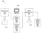
- the semiconductor wafer that is being processed in the processing tool 110 is examined in a review station.
- a review station is a KLA review station.
- One set of data derived from the operation of the review station is a quantitative measure of the amount of misregistration that was caused by the previous exposure process.
- the amount of misregistration relates to the misalignment in the process that occurred between two layers of a semiconductor wafer.
- the amount of misregistration that occurred can be attributed to the control inputs to a particular exposure process.
- the control inputs generally affect the accuracy of the process steps performed by the exposure tools on the semiconductor wafer.
- the control input signals affect the reticle magnification and the position of the semiconductor wafer that is being processed. Modifications of the control inputs can be utilized to improve the performance of the process steps employed in the exposure tool.
- the modifications to the control input signals on the line 120 are based on the effects of external variables on the semiconductor devices being processed.
- FIG. 2 illustrates a first process step 210 , a second process step 220 , a third process step 230 through an Nth process step 240 .
- the latency calculator 158 calculates a latency time (t 1 ) between the first process step 210 and the second process step 220 , as illustrated in FIG. 2 .
- the latency time, t 1 is sent to the feedback/feed-forward controller 160 .
- the feedback/feed-forward controller 160 in conjunction with the computer system 130 and the manufacturing model 140 , utilizes the latency time, t 1 , as a control input parameter.
- the latency time, t 1 is sent to the second through Nth process steps 220 , 230 , 240 to be used as a control input parameter for improving their respective processing quality.
- the second process step 220 is a photoresist material application process, where photoresist material is applied onto the surface of a semiconductor wafer.
- a process light exposure step must be implemented by the third process step 230 within a certain time period that is known by those skilled in the art. Therefore, the latency time, t 1 , can be used as a factor to control the manufacturing process flow while processing the semiconductor wafers.
- the second process step 220 is a wet cleaning process. If the semiconductor wafer is exposed a certain time period before the next process step is implemented, an undesirable oxidation effect may occur on the semiconductor-wafers. Therefore, the known latency time, t 1 , can be used as a control parameter that controls the manufacturing process flow to prevent excessive delay that may cause oxidation on the semiconductor wafers. Furthermore, if oxidation has indeed occurred on the semiconductor wafer being processed, the latency time, t 1 , can be used as a control parameter by the third process step 230 to determine the amount of cleaning to be performed on the semiconductor wafer. The amount of cleaning performed by the third process step 230 will be directly proportional to the latency time, ti. The latency time, t 1 , can be used as a control parameter for other process steps that are known to those skilled in the art.
- FIG. 3 a flowchart depiction of the method of utilizing latency time between manufacturing process steps is illustrated.
- a sequence of at least one manufacturing run of semiconductor wafers is processed, as described in block 310 of FIG. 3 .
- the semiconductor wafers are processed by photolithography processing tools.
- Production data, or metrology data, from the semiconductor wafers is acquired and analyzed, as described in block 320 of Figure.
- at least a sample of the processed semiconductor wafers is sent from the processing tools 110 , 112 to the metrology tool 150 .
- the metrology data processing unit 145 collects and correlates the metrology data with specific semiconductor wafer lot number and manufacturing numbers.
- FIG. 4 illustrates a more detailed description of one embodiment of performing latency analysis.
- production data metalology data
- the production data from the two process steps is collected by the latency calculator 158 .
- the latency calculator 158 uses the production data from the two process steps to calculate the latency time between the two process steps, such as the latency time (t 1 ) between the first process step 210 and the second process step 220 , as described in block 420 of FIG. 4 .
- the latency time calculated by the latency calculator 158 is utilized as a control parameter, as described in block 430 of FIG. 4 .
- the latency time between the two process steps is sent to a feedback/feed-forward controller 160 to be used as a control parameter.
- the latency time is implemented into the manufacturing model 140 , as described in block 440 of FIG. 4 .
- the manufacturing model 140 then analyzes the production data associated with the two process steps and implements the latency time into the control input parameters.
- Error data associated with the processing of semiconductor wafers is calculated, as described in block 510 .
- the error data is acquired from one of a plurality of methods known by those skilled in the art. Once the error data is acquired, a determination is made whether the error data is inside the deadband, as described in block 520 of FIG. 5 .
- the step described in block 520 is performed to determine whether an error is sufficiently significant to warrant a change in the control inputs on the line 120 .
- the errors acquired from product analysis stations (not shown), such as the review station, are compared to a predetermined set of threshold parameters.
- the deadband contains a range of error values associated with control input signals centered proximate to a set of corresponding predetermined target values, for which generally controller action is blocked. If any one of the errors acquired from the product analysis station is smaller than its corresponding predetermined threshold value, that particular error is deemed to be in the deadband.
- One of the primary purposes of the deadband is to prevent excessive control actions, resulting from changes to control input parameters on the line 120 , from causing a semiconductor manufacturing process to be inordinately jittery.
- the principles taught by the present invention can be implemented in an Advanced Process Control (APC) framework.
- the APC framework is a preferred platform from which to implement the overlay control strategy taught by the present invention.
- the APC framework can be a factory-wide software system, therefore, the control strategies taught by the present invention can be applied to virtually any of the semiconductor manufacturing tools on the factory floor.
- the APC framework also allows for remote access and monitoring of the process performance.
- data storage can be more convenient, more flexible, and less expensive than local drives.
- the APC platform allows for more sophisticated types of control because it provides a significant amount of flexibility in writing the necessary software code.
- Deployment of the control strategy taught by the present invention onto the APC framework could require a number of software components.
- a computer script is written for each of the semiconductor manufacturing tools involved in the control system.
- a semiconductor manufacturing tool in the control system When a semiconductor manufacturing tool in the control system is started in the semiconductor manufacturing fab, it generally calls upon a script to initiate the action that is required by the process controller, such as the overlay controller.
- the control methods are generally defined and performed in these scripts.
- the development of these scripts can comprise a significant portion of the development of a control system.
- the principles taught by the present invention can be implemented into other types of manufacturing frameworks.
Abstract
Description
Claims (30)
Priority Applications (1)
| Application Number | Priority Date | Filing Date | Title |
|---|---|---|---|
| US09/749,293 US6571371B1 (en) | 2000-12-27 | 2000-12-27 | Method and apparatus for using latency time as a run-to-run control parameter |
Applications Claiming Priority (1)
| Application Number | Priority Date | Filing Date | Title |
|---|---|---|---|
| US09/749,293 US6571371B1 (en) | 2000-12-27 | 2000-12-27 | Method and apparatus for using latency time as a run-to-run control parameter |
Publications (1)
| Publication Number | Publication Date |
|---|---|
| US6571371B1 true US6571371B1 (en) | 2003-05-27 |
Family
ID=25013130
Family Applications (1)
| Application Number | Title | Priority Date | Filing Date |
|---|---|---|---|
| US09/749,293 Expired - Lifetime US6571371B1 (en) | 2000-12-27 | 2000-12-27 | Method and apparatus for using latency time as a run-to-run control parameter |
Country Status (1)
| Country | Link |
|---|---|
| US (1) | US6571371B1 (en) |
Cited By (11)
| Publication number | Priority date | Publication date | Assignee | Title |
|---|---|---|---|---|
| US20050071038A1 (en) * | 2003-09-30 | 2005-03-31 | Tokyo Electron Limited | System and method for using first-principles simulation to control a semiconductor manufacturing process |
| US20050071034A1 (en) * | 2003-09-30 | 2005-03-31 | Tokyo Electron Limited | System and method for using first-principles simulation to facilitate a semiconductor manufacturing process |
| US20050071035A1 (en) * | 2003-09-30 | 2005-03-31 | Tokyo Electron Limited | System and method for using first-principles simulation to control a semiconductor manufacturing process |
| US20050071037A1 (en) * | 2003-09-30 | 2005-03-31 | Tokyo Electron Limited | System and method for using first-principles simulation to analyze a process performed by a semiconductor processing tool |
| US20050071036A1 (en) * | 2003-09-30 | 2005-03-31 | Tokyo Electron Limited | System and method for using first-principles simulation to characterize a semiconductor manufacturing process |
| US20050106863A1 (en) * | 2003-11-13 | 2005-05-19 | Taiwan Semiconductor Manufacturing Co., Ltd. | Semiconductor wafer manufacturing methods employing cleaning delay period |
| US20050261796A1 (en) * | 2004-05-20 | 2005-11-24 | Taiwan Semiconductor Manufacturing Co., Ltd. | System and method for improving equipment communication in semiconductor manufacturing equipment |
| US6980873B2 (en) | 2004-04-23 | 2005-12-27 | Taiwan Semiconductor Manufacturing Company, Ltd. | System and method for real-time fault detection, classification, and correction in a semiconductor manufacturing environment |
| US20080195857A1 (en) * | 2007-02-09 | 2008-08-14 | Sony Corporation | Techniques For Automatic Registration Of Appliances |
| US20090306941A1 (en) * | 2006-05-15 | 2009-12-10 | Michael Kotelyanskii | Structure Model description and use for scatterometry-based semiconductor manufacturing process metrology |
| US20130064415A1 (en) * | 2011-09-09 | 2013-03-14 | Takumi Ota | Template cleaning apparatus and template cleaning method |
Citations (6)
| Publication number | Priority date | Publication date | Assignee | Title |
|---|---|---|---|---|
| US3845286A (en) * | 1973-02-05 | 1974-10-29 | Ibm | Manufacturing control system for processing workpieces |
| US5375061A (en) * | 1990-11-27 | 1994-12-20 | Kabushiki Kaisha Toshiba | Manufacturing management and apparatus for a semiconductor device |
| US5408405A (en) * | 1993-09-20 | 1995-04-18 | Texas Instruments Incorporated | Multi-variable statistical process controller for discrete manufacturing |
| US5975740A (en) * | 1996-05-28 | 1999-11-02 | Applied Materials, Inc. | Apparatus, method and medium for enhancing the throughput of a wafer processing facility using a multi-slot cool down chamber and a priority transfer scheme |
| US6304999B1 (en) * | 2000-10-23 | 2001-10-16 | Advanced Micro Devices, Inc. | Method and apparatus for embedded process control framework in tool systems |
| US6405144B1 (en) * | 2000-01-18 | 2002-06-11 | Advanced Micro Devices, Inc. | Method and apparatus for programmed latency for improving wafer-to-wafer uniformity |
-
2000
- 2000-12-27 US US09/749,293 patent/US6571371B1/en not_active Expired - Lifetime
Patent Citations (6)
| Publication number | Priority date | Publication date | Assignee | Title |
|---|---|---|---|---|
| US3845286A (en) * | 1973-02-05 | 1974-10-29 | Ibm | Manufacturing control system for processing workpieces |
| US5375061A (en) * | 1990-11-27 | 1994-12-20 | Kabushiki Kaisha Toshiba | Manufacturing management and apparatus for a semiconductor device |
| US5408405A (en) * | 1993-09-20 | 1995-04-18 | Texas Instruments Incorporated | Multi-variable statistical process controller for discrete manufacturing |
| US5975740A (en) * | 1996-05-28 | 1999-11-02 | Applied Materials, Inc. | Apparatus, method and medium for enhancing the throughput of a wafer processing facility using a multi-slot cool down chamber and a priority transfer scheme |
| US6405144B1 (en) * | 2000-01-18 | 2002-06-11 | Advanced Micro Devices, Inc. | Method and apparatus for programmed latency for improving wafer-to-wafer uniformity |
| US6304999B1 (en) * | 2000-10-23 | 2001-10-16 | Advanced Micro Devices, Inc. | Method and apparatus for embedded process control framework in tool systems |
Non-Patent Citations (7)
| Title |
|---|
| Bond et al., "Use of Multiple Lithography Monitors in a Defect Control Strategy for High Volume Manufacturing", 1999 IEEE/SEMI Advanced Semiconductor Manufacturing Conference and Workshop, Sep. 8-10, 1999, pp. 265-269. |
| Herrmann et al., "Evaluating the Impact of Process Changes on Cluster Tool Performance", IEEE Transactions on Semiconductor Manufacturing, vol. 13, No. 2, May 2000, pp. 181-192.* * |
| Lee et al., "Yield Analysis and Data Management Using Yield Manager/sup TM/", 1998 IEEE/SEMI Advanced Semiconductor Manufacturing Conference and Workshop, 23025 Sep. 1998, pp. 19-30. |
| Lu et al., "Education in Semiconductor Manufacturing Processes Through Physically-based Simulation", Proceedings of 26th Annual Conference on Frontiers in Education Conference, Nov. 6-9, 1996, vol. 1, pp. 250-253. |
| Poolsup et al., "Cluster Tool Simulation Assists the System Design", Proceedings of Winter Simulation Conference, vol. 2, Dec. 10-13, 2000, pp. 1443-1448.* * |
| Schaper et al., "Control of MMST RTP: Repeatability, Uniformity, and Integration for Flexible Manufacturing", IEEE Transactions on Semiconductor Manufacturing, vol. 7, No. 2, May 1994, pp. 202-219.* * |
| Warnick et al., "Feedback Synchronization: A Relaxation of Tracking", Proceedings of the American Control Conference, vol. 4, Jun. 28-30, 2000, pp. 2824-2828.* * |
Cited By (22)
| Publication number | Priority date | Publication date | Assignee | Title |
|---|---|---|---|---|
| US8014991B2 (en) * | 2003-09-30 | 2011-09-06 | Tokyo Electron Limited | System and method for using first-principles simulation to characterize a semiconductor manufacturing process |
| US20050071035A1 (en) * | 2003-09-30 | 2005-03-31 | Tokyo Electron Limited | System and method for using first-principles simulation to control a semiconductor manufacturing process |
| US8296687B2 (en) * | 2003-09-30 | 2012-10-23 | Tokyo Electron Limited | System and method for using first-principles simulation to analyze a process performed by a semiconductor processing tool |
| US20050071037A1 (en) * | 2003-09-30 | 2005-03-31 | Tokyo Electron Limited | System and method for using first-principles simulation to analyze a process performed by a semiconductor processing tool |
| US20050071036A1 (en) * | 2003-09-30 | 2005-03-31 | Tokyo Electron Limited | System and method for using first-principles simulation to characterize a semiconductor manufacturing process |
| US20050071039A1 (en) * | 2003-09-30 | 2005-03-31 | Tokyo Electron Limited | System and method for using first-principles simulation to provide virtual sensors that facilitate a semiconductor manufacturing process |
| WO2005034182A2 (en) * | 2003-09-30 | 2005-04-14 | Tokyo Electron Limited | System and method for using first-principles simulation to analyze a process performed by a semiconductor processing tool |
| US8073667B2 (en) * | 2003-09-30 | 2011-12-06 | Tokyo Electron Limited | System and method for using first-principles simulation to control a semiconductor manufacturing process |
| US8050900B2 (en) * | 2003-09-30 | 2011-11-01 | Tokyo Electron Limited | System and method for using first-principles simulation to provide virtual sensors that facilitate a semiconductor manufacturing process |
| WO2005034182A3 (en) * | 2003-09-30 | 2005-09-09 | Tokyo Electron Ltd | System and method for using first-principles simulation to analyze a process performed by a semiconductor processing tool |
| US8036869B2 (en) * | 2003-09-30 | 2011-10-11 | Tokyo Electron Limited | System and method for using first-principles simulation to control a semiconductor manufacturing process via a simulation result or a derived empirical model |
| US20050071034A1 (en) * | 2003-09-30 | 2005-03-31 | Tokyo Electron Limited | System and method for using first-principles simulation to facilitate a semiconductor manufacturing process |
| US8032348B2 (en) * | 2003-09-30 | 2011-10-04 | Tokyo Electron Limited | System and method for using first-principles simulation to facilitate a semiconductor manufacturing process |
| US20050071038A1 (en) * | 2003-09-30 | 2005-03-31 | Tokyo Electron Limited | System and method for using first-principles simulation to control a semiconductor manufacturing process |
| US6933157B2 (en) * | 2003-11-13 | 2005-08-23 | Taiwan Semiconductor Manufacturing Company, Ltd. | Semiconductor wafer manufacturing methods employing cleaning delay period |
| US20050106863A1 (en) * | 2003-11-13 | 2005-05-19 | Taiwan Semiconductor Manufacturing Co., Ltd. | Semiconductor wafer manufacturing methods employing cleaning delay period |
| US6980873B2 (en) | 2004-04-23 | 2005-12-27 | Taiwan Semiconductor Manufacturing Company, Ltd. | System and method for real-time fault detection, classification, and correction in a semiconductor manufacturing environment |
| US7437404B2 (en) | 2004-05-20 | 2008-10-14 | Taiwan Semiconductor Manufacturing Company, Ltd. | System and method for improving equipment communication in semiconductor manufacturing equipment |
| US20050261796A1 (en) * | 2004-05-20 | 2005-11-24 | Taiwan Semiconductor Manufacturing Co., Ltd. | System and method for improving equipment communication in semiconductor manufacturing equipment |
| US20090306941A1 (en) * | 2006-05-15 | 2009-12-10 | Michael Kotelyanskii | Structure Model description and use for scatterometry-based semiconductor manufacturing process metrology |
| US20080195857A1 (en) * | 2007-02-09 | 2008-08-14 | Sony Corporation | Techniques For Automatic Registration Of Appliances |
| US20130064415A1 (en) * | 2011-09-09 | 2013-03-14 | Takumi Ota | Template cleaning apparatus and template cleaning method |
Similar Documents
| Publication | Publication Date | Title |
|---|---|---|
| US6304999B1 (en) | Method and apparatus for embedded process control framework in tool systems | |
| US6556884B1 (en) | Method and apparatus for interfacing a statistical process control system with a manufacturing process control framework | |
| US6442496B1 (en) | Method and apparatus for dynamic sampling of a production line | |
| US6643557B1 (en) | Method and apparatus for using scatterometry to perform feedback and feed-forward control | |
| US6560503B1 (en) | Method and apparatus for monitoring controller performance using statistical process control | |
| US6405144B1 (en) | Method and apparatus for programmed latency for improving wafer-to-wafer uniformity | |
| US6708075B2 (en) | Method and apparatus for utilizing integrated metrology data as feed-forward data | |
| US6427093B1 (en) | Method and apparatus for optimal wafer-by-wafer processing | |
| US6449524B1 (en) | Method and apparatus for using equipment state data for run-to-run control of manufacturing tools | |
| US6773931B2 (en) | Dynamic targeting for a process control system | |
| US6484064B1 (en) | Method and apparatus for running metrology standard wafer routes for cross-fab metrology calibration | |
| EP1208592A1 (en) | Method and apparatus for run-to-run controlling of overlay registration | |
| US6571371B1 (en) | Method and apparatus for using latency time as a run-to-run control parameter | |
| US6645780B1 (en) | Method and apparatus for combining integrated and offline metrology for process control | |
| EP1567920B1 (en) | Secondary process controller for supplementing a primary process controller | |
| US6834213B1 (en) | Process control based upon a metrology delay | |
| US6698009B1 (en) | Method and apparatus for modeling of batch dynamics based upon integrated metrology | |
| US6834211B1 (en) | Adjusting a trace data rate based upon a tool state | |
| US6912436B1 (en) | Prioritizing an application of correction in a multi-input control system | |
| US7797073B1 (en) | Controlling processing of semiconductor wafers based upon end of line parameters | |
| US7120514B1 (en) | Method and apparatus for performing field-to-field compensation | |
| WO2002082534A2 (en) | Method and apparatus for incorporating in-situ sensors |
Legal Events
| Date | Code | Title | Description |
|---|---|---|---|
| AS | Assignment |
Owner name: ADVANCED MICRO DEVICES, INC., TEXAS Free format text: ASSIGNMENT OF ASSIGNORS INTEREST;ASSIGNORS:COSS, JR., ELFIDO;CONBOY, MICHAEL R.;HENDRIX, BRYCE;REEL/FRAME:011424/0428 Effective date: 20001219 |
|
| STCF | Information on status: patent grant |
Free format text: PATENTED CASE |
|
| CC | Certificate of correction | ||
| FPAY | Fee payment |
Year of fee payment: 4 |
|
| AS | Assignment |
Owner name: GLOBALFOUNDRIES INC., CAYMAN ISLANDS Free format text: AFFIRMATION OF PATENT ASSIGNMENT;ASSIGNOR:ADVANCED MICRO DEVICES, INC.;REEL/FRAME:023119/0083 Effective date: 20090630 |
|
| FPAY | Fee payment |
Year of fee payment: 8 |
|
| FPAY | Fee payment |
Year of fee payment: 12 |
|
| AS | Assignment |
Owner name: WILMINGTON TRUST, NATIONAL ASSOCIATION, DELAWARE Free format text: SECURITY AGREEMENT;ASSIGNOR:GLOBALFOUNDRIES INC.;REEL/FRAME:049490/0001 Effective date: 20181127 |
|
| AS | Assignment |
Owner name: GLOBALFOUNDRIES U.S. INC., CALIFORNIA Free format text: ASSIGNMENT OF ASSIGNORS INTEREST;ASSIGNOR:GLOBALFOUNDRIES INC.;REEL/FRAME:054633/0001 Effective date: 20201022 |
|
| AS | Assignment |
Owner name: GLOBALFOUNDRIES INC., CAYMAN ISLANDS Free format text: RELEASE BY SECURED PARTY;ASSIGNOR:WILMINGTON TRUST, NATIONAL ASSOCIATION;REEL/FRAME:054636/0001 Effective date: 20201117 |
|
| AS | Assignment |
Owner name: GLOBALFOUNDRIES U.S. INC., NEW YORK Free format text: RELEASE BY SECURED PARTY;ASSIGNOR:WILMINGTON TRUST, NATIONAL ASSOCIATION;REEL/FRAME:056987/0001 Effective date: 20201117 |