US6589850B1 - Method and system for fabricating a bipolar transistor and related structure - Google Patents
Method and system for fabricating a bipolar transistor and related structure Download PDFInfo
- Publication number
- US6589850B1 US6589850B1 US10/163,661 US16366102A US6589850B1 US 6589850 B1 US6589850 B1 US 6589850B1 US 16366102 A US16366102 A US 16366102A US 6589850 B1 US6589850 B1 US 6589850B1
- Authority
- US
- United States
- Prior art keywords
- chamber
- wafer
- undoped
- base layer
- doped
- Prior art date
- Legal status (The legal status is an assumption and is not a legal conclusion. Google has not performed a legal analysis and makes no representation as to the accuracy of the status listed.)
- Expired - Lifetime
Links
- 238000000034 method Methods 0.000 title claims abstract description 43
- 229910000577 Silicon-germanium Inorganic materials 0.000 claims description 32
- 239000002019 doping agent Substances 0.000 claims description 30
- LEVVHYCKPQWKOP-UHFFFAOYSA-N [Si].[Ge] Chemical compound [Si].[Ge] LEVVHYCKPQWKOP-UHFFFAOYSA-N 0.000 claims description 20
- 230000008569 process Effects 0.000 claims description 14
- ZOXJGFHDIHLPTG-UHFFFAOYSA-N Boron Chemical group [B] ZOXJGFHDIHLPTG-UHFFFAOYSA-N 0.000 claims description 10
- 229910052796 boron Inorganic materials 0.000 claims description 10
- 238000005229 chemical vapour deposition Methods 0.000 claims description 3
- 238000012546 transfer Methods 0.000 abstract description 26
- 235000012431 wafers Nutrition 0.000 description 66
- 239000000463 material Substances 0.000 description 42
- 239000004065 semiconductor Substances 0.000 description 22
- 238000004519 manufacturing process Methods 0.000 description 18
- 229910052710 silicon Inorganic materials 0.000 description 13
- 239000010703 silicon Substances 0.000 description 13
- 229910052732 germanium Inorganic materials 0.000 description 11
- GNPVGFCGXDBREM-UHFFFAOYSA-N germanium atom Chemical compound [Ge] GNPVGFCGXDBREM-UHFFFAOYSA-N 0.000 description 11
- 238000000151 deposition Methods 0.000 description 10
- 238000013459 approach Methods 0.000 description 8
- 230000008021 deposition Effects 0.000 description 7
- 238000012545 processing Methods 0.000 description 7
- OKTJSMMVPCPJKN-UHFFFAOYSA-N Carbon Chemical compound [C] OKTJSMMVPCPJKN-UHFFFAOYSA-N 0.000 description 6
- 229910052799 carbon Inorganic materials 0.000 description 6
- 230000008901 benefit Effects 0.000 description 5
- 239000000758 substrate Substances 0.000 description 5
- 238000005137 deposition process Methods 0.000 description 4
- 230000015572 biosynthetic process Effects 0.000 description 3
- 238000002955 isolation Methods 0.000 description 3
- 230000004044 response Effects 0.000 description 3
- 230000003750 conditioning effect Effects 0.000 description 2
- 238000007796 conventional method Methods 0.000 description 2
- JBRZTFJDHDCESZ-UHFFFAOYSA-N AsGa Chemical compound [As]#[Ga] JBRZTFJDHDCESZ-UHFFFAOYSA-N 0.000 description 1
- 229910001218 Gallium arsenide Inorganic materials 0.000 description 1
- 238000009825 accumulation Methods 0.000 description 1
- 230000002411 adverse Effects 0.000 description 1
- 230000002860 competitive effect Effects 0.000 description 1
- 230000001143 conditioned effect Effects 0.000 description 1
- 239000000470 constituent Substances 0.000 description 1
- 230000008878 coupling Effects 0.000 description 1
- 238000010168 coupling process Methods 0.000 description 1
- 238000005859 coupling reaction Methods 0.000 description 1
- 239000013078 crystal Substances 0.000 description 1
- 238000009792 diffusion process Methods 0.000 description 1
- 230000000694 effects Effects 0.000 description 1
- 238000005516 engineering process Methods 0.000 description 1
- 238000005530 etching Methods 0.000 description 1
- 238000012986 modification Methods 0.000 description 1
- 230000004048 modification Effects 0.000 description 1
- 229910021421 monocrystalline silicon Inorganic materials 0.000 description 1
- 230000037361 pathway Effects 0.000 description 1
- 229910021420 polycrystalline silicon Inorganic materials 0.000 description 1
- 238000002360 preparation method Methods 0.000 description 1
- 238000003672 processing method Methods 0.000 description 1
- 230000008707 rearrangement Effects 0.000 description 1
- 238000006467 substitution reaction Methods 0.000 description 1
Images


Classifications
-
- H—ELECTRICITY
- H01—ELECTRIC ELEMENTS
- H01L—SEMICONDUCTOR DEVICES NOT COVERED BY CLASS H10
- H01L29/00—Semiconductor devices adapted for rectifying, amplifying, oscillating or switching, or capacitors or resistors with at least one potential-jump barrier or surface barrier, e.g. PN junction depletion layer or carrier concentration layer; Details of semiconductor bodies or of electrodes thereof ; Multistep manufacturing processes therefor
- H01L29/66—Types of semiconductor device ; Multistep manufacturing processes therefor
- H01L29/66007—Multistep manufacturing processes
- H01L29/66075—Multistep manufacturing processes of devices having semiconductor bodies comprising group 14 or group 13/15 materials
- H01L29/66227—Multistep manufacturing processes of devices having semiconductor bodies comprising group 14 or group 13/15 materials the devices being controllable only by the electric current supplied or the electric potential applied, to an electrode which does not carry the current to be rectified, amplified or switched, e.g. three-terminal devices
- H01L29/66234—Bipolar junction transistors [BJT]
- H01L29/66242—Heterojunction transistors [HBT]
Definitions
- the present invention is generally in the field of semiconductor fabrication. More particularly, the present invention is in the field of fabrication of bipolar transistors.
- Bipolar transistors are commonly used in electronic devices and, in particular, in radio frequency applications.
- a particular type of bipolar transistor which is used as an example in the present application, is the silicon-germanium (“SiGe”) heterojunction bipolar transistor (“HBT”) in which a thin layer of silicon-germanium is grown over the bipolar transistor's collector region to operate as the base of the bipolar transistor.
- SiGe silicon-germanium
- HBT heterojunction bipolar transistor
- the silicon-germanium HBT has significant advantages in speed, frequency response, and gain when compared to a conventional silicon-only bipolar transistor, for instance. Cutoff frequencies in excess of 100 GHz, which are comparable to the more expensive gallium-arsenide based devices, have been achieved for the silicon-germanium HBT.
- the higher gain, speed and frequency response of the silicon-germanium HBT are possible due to certain advantages of silicon-germaniurn, such as a narrower band gap and reduced resistivity. These advantages make silicon-gernanium devices more competitive than silicon-only devices in areas of technology where superior speed and frequency response are required.
- FIG. 1 illustrates bipolar structure 100 , which in the present example is a silicon-germanium HBT structure.
- structure 100 includes, among other components, collector 130 , silicon-germanium base 120 , and emitter 140 .
- collector 130 is N type single-crystal silicon
- base 120 is P type single-crystal silicon-germanium.
- base 120 can be fabricated epitaxially, for example, in a reduced pressure chemical vapor deposition process (“RPCVD”), to grow a silicon-germanium film over top surface 132 of collector 130 .
- RPCVD reduced pressure chemical vapor deposition process
- a suitable dopant, such as boron is typically introduced during the silicon-germanium film growth to attain the desired electrical properties of the base.
- structure 100 further includes emitter 140 , which is situated above and forms a junction with base 120 , and which is comprised of N type polycrystalline silicon.
- the interface between emitter 140 , base 120 , and collector 130 is the active region of the NPN silicon-germanium HBT, i.e., structure 100 .
- dielectric segments 142 provide electrical isolation to emitter 140 from base 120 .
- buried layer 134 which is composed of N+ type material, is formed in semiconductor substrate 110 .
- Collector sinker 136 also composed of N+ type material, is formed by diffusion of heavily concentrated dopants from the surface of collector sinker 136 down to buried layer 134 .
- Buried layer 134 and collector sinker 136 provide a low resistance electrical pathway from collector 130 through buried layer 134 and collector sinker 136 to a collector contact (not shown).
- Deep trench structures 133 and field oxide regions 138 provide electrical isolation from other devices on semiconductor substrate 110 .
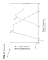
- graph 200 illustrates the doping profile of the base in an exemplary silicon-germanium HBT, such as the NPN silicon-germanium HBT structure of structure 100 in FIG. 1 .
- y-axis 202 plots the concentration level of materials (e.g., germanium and other dopants) that are deposited along with silicon over the collector as part of growing the base
- x-axis 204 plots the thickness of the base as the deposition proceeds.
- the origin (i.e., the intersection of y-axis 202 and x-axis 204 ) of graph 200 corresponds to the top surface of the collector over which the silicon-germanium base is grown, at the point where fabrication of the base is to begin with the deposition of silicon only.
- germanium is introduced into the deposition process and grows along with the silicon over the collector.
- Profile 206 illustrates the doping profile of the germanium.
- a suitable dopant is introduced into the mix with the silicon and germanium, and the concentration level of the dopant is shown by profile 208 .
- the dopant can be boron, for example.
- a wafer having a transistor region over which the silicon-germarnium base is to be grown is initially baked in a reactor chamber at approximately 900° C. for approximately five minutes. Subsequently, the chamber is cooled down to between 600° C. and 750° C. so that the desired base materials, for example silicon-germnanium and boron, can be deposited. According to this method, the formation of the base typically requires between approximately five and ten minutes to complete, after which time the wafer is removed from the reactor chamber.
- the chamber has to undergo extensive conditioning in preparation for the next wafer.
- the conditioning is necessary due to, for instance, the accumulation of materials on the chamber wall from previous deposition procedures that can adversely impact the processing of subsequent wafers. More specifically, a primary concern is the presence of residual dopant materials, such as boron, on the chamber walls which can contaminate subsequent wafers and compromise the electrical properties of the base layer formed on these subsequent wafers.
- a chamber etching step is needed after the processing of each wafer to remove the undesired materials from the chamber.
- the chamber temperature has to be raised to approximately 1100° C., and an etchant, for example HCI gas, is supplied to etch the dopant or undesired materials, along with the silicon and germanium, from the chamber walls.
- an etchant for example HCI gas
- the etchant is evacuated out of the chamber.
- the chamber temperature has to then be lowered to approximately 900° C. before the next wafer can be processed.
- the need to clean the chamber after each wafer introduces a significant time and cost budget on manufacturers.
- the time required to clean the chamber translates to lower throughput and productivity and to higher manufacturing cost.
- Some manufacturers have tried to increase throughput by, for example, baking the wafers in a separate bake chamber and coupling the bake chamber to multiple epi chambers, wherein deposition of the base can occur. In this manner, wafers can be processed more quickly since one epi chamber can be depositing while the other epi chamber is being cleaned.
- the separate bake chamber supplies a steady number of wafers to the epi chambers.
- an epi chamber still needs to be cleaned after every wafer to remove the undesired materials accumulated on the chamber walls.
- the present invention is directed to method and system for fabricating a bipolar transistor and related structure.
- the present invention overcomes the need in the art for an approach for fabricating bipolar transistors, such as a silicon-germanium (“SiGe”) heterojunction bipolar transistor (“HBT”), that is more efficient than conventional approaches, and which will increase throughput without imposing additional significant costs.
- SiGe silicon-germanium
- HBT heterojunction bipolar transistor
- the invention is a method for fabricating the base of a bipolar transistor where the method comprises placing a first wafer in an undoped epi chamber.
- the first wafer is baked in a separate bake chamber prior to placing it (i.e. the first wafer) in the undoped epi chamber.
- a first undoped base layer is grown over the first wafer.
- the first undoped base layer can comprise a SiGe layer when the exemplary bipolar transistor is a SiGe HBT.
- the first wafer is transferred from the undoped epi chamber into a separate doped epi chamber.
- a first doped base layer is then grown over the first undoped based layer in the doped epi chamber.
- the dopant might be boron.
- a second wafer can be processed in the undoped epi chamber.
- the invention is a structure produced by the above method and, in yet another embodiment, the invention comprises a transfer chamber, a transfer arm, a bake chamber, and a separate undoped epi chamber and a doped epi chamber for practicing the invention's method.
- the present invention results in a fabrication approach that is more efficient than conventional fabrication techniques, and which will increase throughput without imposing additional significant costs.
- FIG. 1 illustrates a cross sectional view of some of the features of a bipolar transistor fabricated utilizing conventional methods.
- FIG. 2 shows the doping profile of one type of bipolar transistor.
- FIG. 3 illustrates a system for growing a base in a bipolar transistor in accordance with one embodiment of the present invention.
- FIG. 4 shows a flowchart illustrating some exemplary steps taken to implement an embodiment of the invention.
- FIG. 5 illustrates a cross sectional view of some of the features of a bipolar transistor fabricated in accordance with one embodiment of the present invention.
- the present invention is directed to method and system for fabricating a bipolar transistor and related structure.
- the following description contains specific information pertaining to the implementation of the present invention.
- One skilled in the art will recognize that the present invention may be implemented in a manner different from that specifically discussed in the present application. Moreover, some of the specific details of the invention are not discussed in order not to obscure the invention. The specific details not described in the present application are within the knowledge of a person of ordinary skill in the art.
- FIG. 3 Illustrated in FIG. 3 is exemplary wafer processing system 300 , which is used to describe the fabrication of an exemplary base in an exemplary bipolar transistor, in accordance with one embodiment of the present invention.
- an exemplary silicon-germanium (“SiGe”) base in a SiGe heterojunction bipolar transistor (“HBT”) is used for the purpose of illustrating the invention's concepts by referring to specifics.
- SiGe silicon-germanium
- HBT SiGe heterojunction bipolar transistor
- the concepts and techniques of the present invention applies also to bipolar transistors other than SiGe HBTs and that the invention is not limited to the specific examples provided in the present application.
- certain details and features, which are apparent to a person of ordinary skill in the art, have been left out of FIG. 3 in order not to obscure the concepts of the present invention.
- system 300 includes transfer chamber 310 , in which is situated transfer arm 312 .
- Loadlock 314 is attached to transfer chamber 310 and contains wafers awaiting further processing.
- loadlock 314 may have end-patterned wafers comprising transistor regions over which the base is to be fabricated. It is to be understood that end-patterned wafers comprise, among other features, transistor regions having components of a bipolar transistor prior to the formation of a base layer over the transistor regions.
- the bipolar transistor can include a collector, certain oxide and isolation regions, and other components known generally to those in the art. Wafers in loadlock 314 can be picked up and handled by transfer arm 312 .
- system 300 further includes bake chamber 316 , “undoped” epi chamber 318 , and “doped” epi chamber 320 connected to transfer chamber 310 .
- Bake chamber 316 can be any suitable bake chamber known in the art configured for baking wafers.
- undoped epi chamber 318 and doped epi chamber 320 can be suitable reactors known in the art, in which materials for the base can be deposited.
- undoped epi chamber 318 and doped epi chamber 320 can be configured for chemical vapor deposition (“CVD”) and/or related deposition methods. The temperature of undoped epi chamber 318 and doped epi chamber 320 can be maintained at a desired temperature to facilitate deposition of the base materials.
- CVD chemical vapor deposition
- transfer arm 312 can transfer an end-patterned wafer from loadlock 314 and place the wafer in bake chamber 316 to be baked.
- the temperature of bake chamber 316 can be maintained separately from undoped epi chamber 318 and doped epi chamber 320 .
- the temperature of bake chamber 316 can be maintained at between approximately 800° C. and 1000° C., for example. After a wafer has been in bake chamber 316 for a sufficient length of time, transfer arm 312 can transfer the wafer to undoped epi chamber 318 .
- a first semiconductor such as silicon
- a second semiconductor such as germanium
- the relative concentrations of the first and second semiconductor materials can be controlled in a manner known in the art.
- Other materials, such as carbon, may also be introduced into epi chamber 318 and grown with the semiconductor materials.
- the deposition process in undoped epi chamber 318 ends. In other words, no dopant is introduced into undoped epi chamber 318 .
- the film deposited over the wafer in undoped epi chamber 318 comprises undoped semiconductor material, and the material formed on the walls of undoped epi chamber 318 likewise consists of only semiconductor(s). It is noted that the undoped semiconductor film deposited over the transistor regions of the wafer as part of the base fabrication process is also referred to as an “undoped base layer” in the present application.
- transfer arm 312 can transfer the wafer to doped epi chamber 320 , wherein more materials, including the base dopant, are deposited to complete fabrication of the base.
- doped epi chamber 320 deposition may begin with the introduction of the desired concentrations of semiconductor materials and the dopant into doped epi chamber 320 .
- the semiconductor materials can comprise silicon and germanium, while the dopant can be boron, for example.
- other materials, such as carbon may also be introduced into doped epi chamber 320 and grown with the semiconductor materials and the dopant.
- the relative concentrations of the materials introduced into doped epi chamber 320 can be controlled to achieve the desired electrical properties for the base.
- a second, or “doped,” base layer comprising the semiconductor materials and the dopant material is grown over the undoped base layer formed in undoped epi chamber 318 .
- the doped base layer may also comprise other materials, such as carbon, in some embodiments.
- doped epi chamber 320 As part of the deposition process performed in doped epi chamber 320 , the materials introduced into doped epi chamber 320 accumulate on the walls of doped epi chamber 320 , in addition to growing on the base layer. Consequently, the walls of doped epi chamber 320 may be blanketed with residual dopant material, following formation of the doped base layer. However, because doped epi chamber 320 is used only for growing the doped base layer, and not the undoped base layer, the presence of dopants on the walls of epi chamber 320 has little effect on the processing of a subsequent wafer in doped epi chamber 320 .
- the impact on the resulting base would be minimal, because the dopant is a desired constituent of the doped base layer.
- the present invention achieves greater throughput than conventional bipolar transistor fabrication techniques.
- the increase in throughput is possible because the threat of residual dopant materials on the chamber walls depositing uncontrollably and contaminating the base is averted, since the dopant material is introduced into only the epi chamber where the doped base layer is grown.
- An advantage of the present invention therefore, is that the chambers do not have to be cleaned or conditioned as frequently as conventional fabrication methods. As a result, the present invention achieves greater throughput and substantially reduces manufacturing costs.
- FIG. 4 illustrating exemplary process 400 for fabricating wafers and for growing the base of a bipolar transistor, such as a silicon-germanium HBT, in accordance with one embodiment of the present invention.
- a step may consist of one or more substeps or may involve specialized equipment, as known in the art.
- Process 400 begins at step 410 and continues to step 412 where transfer arm 312 places a first wafer comprising transistor regions over which a base is to be fabricated in bake chamber 316 to be baked.
- a wafer placed in bake chamber 316 can be baked for between approximately one and five minutes at between approximately 800° C. and approximately 1000° C.
- transfer arm 312 removes the first wafer from bake chamber 316 and places it (i.e. the first wafer) in undoped epi chamber 318 , and a second wafer is placed in bake chamber 316 by transfer arm 312 .
- an undoped base layer is deposited over the first wafer in undoped epi chamber 318 .
- the undoped base layer comprises semiconductor materials, such as silicon and germanium, for example. In some embodiments, other materials, such as carbon, may also be deposited as part of the undoped base layer.
- the second wafer is baked in bake chamber 316 .
- transfer arm 312 removes the first wafer from undoped epi chamber 318 and places it (i.e. the first wafer) in doped epi chamber 320 , while the second wafer is transferred into undoped epi chamber 318 by transfer arm 312 , and while a third wafer is placed in bake chamber 316 by transfer arm 312 .
- a doped base layer is then deposited over the undoped base layer of the first wafer in doped epi chamber 320 at step 420 .
- the doped base layer comprises semiconductor materials, such as silicon and germanium, and a desired dopant, such as boron.
- the doped base layer may also comprise other materials, such as carbon.
- an undoped layer is grown over the second wafer in undoped epi chamber 318 , and the third wafer is baked in bake chamber 316 .
- Process 400 then proceeds to step 422 where the first wafer, now having a base comprising an undoped layer and a doped layer, is removed from doped epi chamber 320 by transfer arm 312 .
- step 422 Further processing of the first wafer subsequent to step 422 can be performed in a manner known in the art and is not discussed in detail here.
- the second wafer is removed from undoped epi chamber 318 and transferred to doped epi chamber 320 by transfer arm 312
- the third wafer is removed from bake chamber 316 and placed in undoped epi chamber 318 by transfer arm 312 .
- Process 400 continues at step 424 where a doped base layer is deposited in doped epi chamber 320 over the undoped base layer of the second wafer. Also, at step 424 , an undoped base layer is formed over the third wafer in undoped epi chamber 318 .
- the second wafer having a base comprising an undoped base layer and a doped base layer is removed from doped epi chamber 320 by transfer arm 312 , while the third wafer is transferred from undoped epi chamber 318 to doped epi chamber 320 by transfer arm 312 .
- a doped base layer is deposited over the undoped base layer of the third wafer in doped epi chamber 320 , following which the third wafer is removed from doped epi chamber 320 .
- Process 400 then ends at step 430 .
- exemplary structure 500 is used to describe fabrication of a base in a bipolar transistor, such as a silicon-germanium HBT, in accordance with one embodiment. Certain details and features have been left out of FIG. 5 which are apparent to a person of ordinary skill in the art.
- structure 500 comprises collector 530 having top surface 532 formed in substrate 51 0 .
- Structure 500 further includes field oxides 538 . It is appreciated that collector 530 having top surface 532 , substrate 510 , and field oxides 538 in structure 500 are respectively equivalent to collector 130 having top surface 132 , substrate 110 , and field oxides 138 in structure 100 illustrated in FIG. 1 .
- base 520 is made up of two separate layers, i.e., undoped base layer 522 and doped base layer 524 .
- Undoped base layer 522 in the present embodiment comprises semiconductor materials only, while doped base layer 524 comprises semiconductor materials doped with a desired dopant.
- the semiconductor materials in undoped and doped base layers 522 and 524 can comprise silicon and germanium, while the dopant in doped base layer 524 can be boron, for example.
- base 520 may comprise additional materials, such as carbon.
- base 520 can be fabricated according to the steps of process 400 in FIG. 4, which can be performed by system 300 in FIG. 3 .
- undoped base layer 522 may be formed first in undoped epi chamber 318 wherein only semiconductor materials are deposited, and doped base layer 524 may be separately formed in doped epi chamber 320 , wherein a dopant such as boron is deposited along with the semiconductor materials.
- further processing including the fabrication of an emitter over base 520 , results in a bipolar transistor.
Abstract
Description
Claims (10)
Priority Applications (3)
| Application Number | Priority Date | Filing Date | Title |
|---|---|---|---|
| US10/163,661 US6589850B1 (en) | 2002-06-04 | 2002-06-04 | Method and system for fabricating a bipolar transistor and related structure |
| US10/313,583 US6972442B1 (en) | 2002-06-04 | 2002-12-07 | Efficiently fabricated bipolar transistor |
| US10/313,700 US6830625B1 (en) | 2002-06-04 | 2002-12-07 | System for fabricating a bipolar transistor |
Applications Claiming Priority (1)
| Application Number | Priority Date | Filing Date | Title |
|---|---|---|---|
| US10/163,661 US6589850B1 (en) | 2002-06-04 | 2002-06-04 | Method and system for fabricating a bipolar transistor and related structure |
Related Child Applications (2)
| Application Number | Title | Priority Date | Filing Date |
|---|---|---|---|
| US10/313,583 Division US6972442B1 (en) | 2002-06-04 | 2002-12-07 | Efficiently fabricated bipolar transistor |
| US10/313,700 Division US6830625B1 (en) | 2002-06-04 | 2002-12-07 | System for fabricating a bipolar transistor |
Publications (1)
| Publication Number | Publication Date |
|---|---|
| US6589850B1 true US6589850B1 (en) | 2003-07-08 |
Family
ID=22591010
Family Applications (3)
| Application Number | Title | Priority Date | Filing Date |
|---|---|---|---|
| US10/163,661 Expired - Lifetime US6589850B1 (en) | 2002-06-04 | 2002-06-04 | Method and system for fabricating a bipolar transistor and related structure |
| US10/313,583 Expired - Lifetime US6972442B1 (en) | 2002-06-04 | 2002-12-07 | Efficiently fabricated bipolar transistor |
| US10/313,700 Expired - Lifetime US6830625B1 (en) | 2002-06-04 | 2002-12-07 | System for fabricating a bipolar transistor |
Family Applications After (2)
| Application Number | Title | Priority Date | Filing Date |
|---|---|---|---|
| US10/313,583 Expired - Lifetime US6972442B1 (en) | 2002-06-04 | 2002-12-07 | Efficiently fabricated bipolar transistor |
| US10/313,700 Expired - Lifetime US6830625B1 (en) | 2002-06-04 | 2002-12-07 | System for fabricating a bipolar transistor |
Country Status (1)
| Country | Link |
|---|---|
| US (3) | US6589850B1 (en) |
Cited By (1)
| Publication number | Priority date | Publication date | Assignee | Title |
|---|---|---|---|---|
| US6830625B1 (en) * | 2002-06-04 | 2004-12-14 | Newport Fab, Llc | System for fabricating a bipolar transistor |
Citations (5)
| Publication number | Priority date | Publication date | Assignee | Title |
|---|---|---|---|---|
| US4507169A (en) * | 1981-06-29 | 1985-03-26 | Fujitsu Limited | Method and apparatus for vapor phase growth of a semiconductor |
| US4838201A (en) * | 1986-12-12 | 1989-06-13 | Daido Sanso K. K. | Apparatus and process for vacuum chemical epitaxy |
| US5968279A (en) * | 1997-06-13 | 1999-10-19 | Mattson Technology, Inc. | Method of cleaning wafer substrates |
| US6064081A (en) * | 1994-11-10 | 2000-05-16 | Lawrence Semiconductor Research Laboratory, Inc. | Silicon-germanium-carbon compositions and processes thereof |
| US20020038874A1 (en) * | 2000-09-29 | 2002-04-04 | Kabushiki Kaisha Toshiba | Hetero-bipolar transistor and method of manufacture thereof |
Family Cites Families (7)
| Publication number | Priority date | Publication date | Assignee | Title |
|---|---|---|---|---|
| US5882165A (en) * | 1986-12-19 | 1999-03-16 | Applied Materials, Inc. | Multiple chamber integrated process system |
| JP2569058B2 (en) * | 1987-07-10 | 1997-01-08 | 株式会社日立製作所 | Semiconductor device |
| KR100244041B1 (en) * | 1995-08-05 | 2000-02-01 | 엔도 마코토 | Substrate processing apparatus |
| JP3947761B2 (en) * | 1996-09-26 | 2007-07-25 | 株式会社日立国際電気 | Substrate processing apparatus, substrate transfer machine, and substrate processing method |
| GB2343550A (en) * | 1997-07-29 | 2000-05-10 | Silicon Genesis Corp | Cluster tool method and apparatus using plasma immersion ion implantation |
| US6436194B1 (en) * | 2001-02-16 | 2002-08-20 | Applied Materials, Inc. | Method and a system for sealing an epitaxial silicon layer on a substrate |
| US6589850B1 (en) * | 2002-06-04 | 2003-07-08 | Newport Fab, Llc | Method and system for fabricating a bipolar transistor and related structure |
-
2002
- 2002-06-04 US US10/163,661 patent/US6589850B1/en not_active Expired - Lifetime
- 2002-12-07 US US10/313,583 patent/US6972442B1/en not_active Expired - Lifetime
- 2002-12-07 US US10/313,700 patent/US6830625B1/en not_active Expired - Lifetime
Patent Citations (5)
| Publication number | Priority date | Publication date | Assignee | Title |
|---|---|---|---|---|
| US4507169A (en) * | 1981-06-29 | 1985-03-26 | Fujitsu Limited | Method and apparatus for vapor phase growth of a semiconductor |
| US4838201A (en) * | 1986-12-12 | 1989-06-13 | Daido Sanso K. K. | Apparatus and process for vacuum chemical epitaxy |
| US6064081A (en) * | 1994-11-10 | 2000-05-16 | Lawrence Semiconductor Research Laboratory, Inc. | Silicon-germanium-carbon compositions and processes thereof |
| US5968279A (en) * | 1997-06-13 | 1999-10-19 | Mattson Technology, Inc. | Method of cleaning wafer substrates |
| US20020038874A1 (en) * | 2000-09-29 | 2002-04-04 | Kabushiki Kaisha Toshiba | Hetero-bipolar transistor and method of manufacture thereof |
Cited By (1)
| Publication number | Priority date | Publication date | Assignee | Title |
|---|---|---|---|---|
| US6830625B1 (en) * | 2002-06-04 | 2004-12-14 | Newport Fab, Llc | System for fabricating a bipolar transistor |
Also Published As
| Publication number | Publication date |
|---|---|
| US6972442B1 (en) | 2005-12-06 |
| US6830625B1 (en) | 2004-12-14 |
Similar Documents
| Publication | Publication Date | Title |
|---|---|---|
| US9368608B1 (en) | Heterojunction bipolar transistor with improved performance and breakdown voltage | |
| US7875908B2 (en) | Selective links in silicon hetero-junction bipolar transistors using carbon doping and method of forming same | |
| US9502504B2 (en) | SOI lateral bipolar transistors having surrounding extrinsic base portions | |
| JP4391069B2 (en) | Hetero bipolar transistor and manufacturing method thereof | |
| US7413967B2 (en) | Yield improvement in silicon-germanium epitaxial growth | |
| US7786510B2 (en) | Transistor structure and manufacturing method thereof | |
| US6346452B1 (en) | Method for controlling an N-type dopant concentration depth profile in bipolar transistor epitaxial layers | |
| US7507642B2 (en) | Vapor-phase growth method, semiconductor manufacturing method and semiconductor device manufacturing method | |
| JPH05129319A (en) | Transistor structure with epitaxial-base region and manufacture thereof | |
| US20060163625A1 (en) | Semiconductor layer and forming method thereof, and semiconductor device and manufacturing method thereof technical field | |
| US6861324B2 (en) | Method of forming a super self-aligned hetero-junction bipolar transistor | |
| US6589850B1 (en) | Method and system for fabricating a bipolar transistor and related structure | |
| EP0800705B1 (en) | Manufacture of a semiconductor device with selectively deposited semiconductor zone | |
| US7012009B2 (en) | Method for improving the electrical continuity for a silicon-germanium film across a silicon/oxide/polysilicon surface using a novel two-temperature process | |
| US6744080B2 (en) | Method of manufacturing a bipolar transistor of double-polysilicon, heterojunction-base type and corresponding transistor | |
| US10243065B2 (en) | Method of manufacturing SOI lateral Si-emitter SiGe base HBT | |
| US6660607B2 (en) | Method for fabricating heterojunction bipolar transistors | |
| US6861308B2 (en) | Method for fabrication of SiGe layer having small poly grains and related structure | |
| JP2003514394A (en) | Method of manufacturing semiconductor device having SiGe heterojunction bipolar transistor | |
| US20230088544A1 (en) | Dopant profile control in heterojunction bipolar transistor (hbt) | |
| KR20040029526A (en) | Heterojunction bipolar transistor and method for manufacturing the same | |
| JPH021933A (en) | Manufacture of semiconductor device | |
| WO2004077570A1 (en) | Bipolar transistor and integrated circuit device | |
| KR20050060404A (en) | Fabrication methode of heterojunction bipolar transistor |
Legal Events
| Date | Code | Title | Description |
|---|---|---|---|
| AS | Assignment |
Owner name: CONEXANT SYSTEMS, INC., CALIFORNIA Free format text: ASSIGNMENT OF ASSIGNORS INTEREST;ASSIGNOR:SCHUEGRAF, KLAUS F.;REEL/FRAME:012985/0590 Effective date: 20020522 |
|
| STCF | Information on status: patent grant |
Free format text: PATENTED CASE |
|
| AS | Assignment |
Owner name: NEWPORT FAB, LLC, DBA JAZZ SEMICONDUCTOR, CALIFORN Free format text: ASSIGNMENT OF ASSIGNORS INTEREST;ASSIGNOR:CONEXANT SYSTEMS, INC.;REEL/FRAME:016613/0874 Effective date: 20050525 |
|
| AS | Assignment |
Owner name: WACHOVIA CAPITAL FINANCE CORPORATION (WESTERN), CA Free format text: SECURITY AGREEMENT;ASSIGNOR:NEWPORT FAB, LLC;REEL/FRAME:017223/0083 Effective date: 20060106 |
|
| AS | Assignment |
Owner name: WACHOVIA CAPITAL FINANCE CORPORATION (WESTERN), CA Free format text: SECURITY AGREEMENT;ASSIGNOR:NEWPORT FAB, LLC;REEL/FRAME:017586/0081 Effective date: 20060106 |
|
| FPAY | Fee payment |
Year of fee payment: 4 |
|
| FPAY | Fee payment |
Year of fee payment: 8 |
|
| REMI | Maintenance fee reminder mailed | ||
| FPAY | Fee payment |
Year of fee payment: 12 |
|
| SULP | Surcharge for late payment |
Year of fee payment: 11 |
|
| AS | Assignment |
Owner name: NEWPORT FAB, LLC DBA JAZZ SEMICONDUCTOR OPERATING COMPANY, CALIFORNIA Free format text: RELEASE BY SECURED PARTY;ASSIGNOR:WELLS FARGO CAPITAL FINANCE, LLC, AS SUCCESSOR BY MERGER TO WACHOVIA CAPITAL FINANCE CORPORATION (WESTERN);REEL/FRAME:065284/0123 Effective date: 20230929 |