US6590545B2 - Electrically small planar UWB antenna apparatus and related system - Google Patents
Electrically small planar UWB antenna apparatus and related system Download PDFInfo
- Publication number
- US6590545B2 US6590545B2 US10/054,790 US5479002A US6590545B2 US 6590545 B2 US6590545 B2 US 6590545B2 US 5479002 A US5479002 A US 5479002A US 6590545 B2 US6590545 B2 US 6590545B2
- Authority
- US
- United States
- Prior art keywords
- driven element
- antenna device
- recited
- transmission line
- antenna
- Prior art date
- Legal status (The legal status is an assumption and is not a legal conclusion. Google has not performed a legal analysis and makes no representation as to the accuracy of the status listed.)
- Expired - Fee Related
Links
- 230000005540 biological transmission Effects 0.000 claims description 164
- 239000004020 conductor Substances 0.000 claims description 32
- 239000002184 metal Substances 0.000 claims description 21
- 229910052751 metal Inorganic materials 0.000 claims description 21
- 239000004809 Teflon Substances 0.000 claims description 15
- 229920006362 Teflon® Polymers 0.000 claims description 15
- 239000011152 fibreglass Substances 0.000 claims description 14
- RYGMFSIKBFXOCR-UHFFFAOYSA-N Copper Chemical compound [Cu] RYGMFSIKBFXOCR-UHFFFAOYSA-N 0.000 claims description 13
- 229910052802 copper Inorganic materials 0.000 claims description 13
- 239000010949 copper Substances 0.000 claims description 13
- 239000003570 air Substances 0.000 claims description 10
- 239000000758 substrate Substances 0.000 abstract description 14
- 238000010586 diagram Methods 0.000 description 21
- 239000011810 insulating material Substances 0.000 description 15
- 230000005855 radiation Effects 0.000 description 11
- -1 e.g. Substances 0.000 description 10
- 239000012811 non-conductive material Substances 0.000 description 8
- 238000012546 transfer Methods 0.000 description 8
- 230000004044 response Effects 0.000 description 7
- 239000006185 dispersion Substances 0.000 description 6
- 238000004519 manufacturing process Methods 0.000 description 6
- 238000003491 array Methods 0.000 description 5
- 238000013461 design Methods 0.000 description 5
- 239000000463 material Substances 0.000 description 5
- 238000000034 method Methods 0.000 description 5
- 230000007704 transition Effects 0.000 description 5
- 238000012986 modification Methods 0.000 description 4
- 230000004048 modification Effects 0.000 description 4
- 238000013459 approach Methods 0.000 description 3
- 238000004891 communication Methods 0.000 description 3
- 238000010276 construction Methods 0.000 description 3
- 238000002592 echocardiography Methods 0.000 description 3
- 230000005684 electric field Effects 0.000 description 3
- 230000001965 increasing effect Effects 0.000 description 3
- 230000001788 irregular Effects 0.000 description 3
- 229910000679 solder Inorganic materials 0.000 description 3
- 230000003068 static effect Effects 0.000 description 3
- 235000012489 doughnuts Nutrition 0.000 description 2
- 230000010354 integration Effects 0.000 description 2
- 238000001228 spectrum Methods 0.000 description 2
- 229910000859 α-Fe Inorganic materials 0.000 description 2
- 239000011324 bead Substances 0.000 description 1
- 230000008859 change Effects 0.000 description 1
- 230000008878 coupling Effects 0.000 description 1
- 238000010168 coupling process Methods 0.000 description 1
- 238000005859 coupling reaction Methods 0.000 description 1
- 238000005520 cutting process Methods 0.000 description 1
- 230000009977 dual effect Effects 0.000 description 1
- 238000001914 filtration Methods 0.000 description 1
- 239000003292 glue Substances 0.000 description 1
- 230000001939 inductive effect Effects 0.000 description 1
- 230000003993 interaction Effects 0.000 description 1
- 230000002452 interceptive effect Effects 0.000 description 1
- 238000002955 isolation Methods 0.000 description 1
- 230000010363 phase shift Effects 0.000 description 1
- 230000010287 polarization Effects 0.000 description 1
- 230000009467 reduction Effects 0.000 description 1
- 238000004904 shortening Methods 0.000 description 1
- 239000007787 solid Substances 0.000 description 1
- 239000007921 spray Substances 0.000 description 1
Images


Classifications
-
- H—ELECTRICITY
- H01—ELECTRIC ELEMENTS
- H01Q—ANTENNAS, i.e. RADIO AERIALS
- H01Q9/00—Electrically-short antennas having dimensions not more than twice the operating wavelength and consisting of conductive active radiating elements
- H01Q9/04—Resonant antennas
- H01Q9/30—Resonant antennas with feed to end of elongated active element, e.g. unipole
- H01Q9/40—Element having extended radiating surface
-
- H—ELECTRICITY
- H01—ELECTRIC ELEMENTS
- H01Q—ANTENNAS, i.e. RADIO AERIALS
- H01Q13/00—Waveguide horns or mouths; Slot antennas; Leaky-waveguide antennas; Equivalent structures causing radiation along the transmission path of a guided wave
- H01Q13/08—Radiating ends of two-conductor microwave transmission lines, e.g. of coaxial lines, of microstrip lines
- H01Q13/085—Slot-line radiating ends
-
- H—ELECTRICITY
- H01—ELECTRIC ELEMENTS
- H01Q—ANTENNAS, i.e. RADIO AERIALS
- H01Q15/00—Devices for reflection, refraction, diffraction or polarisation of waves radiated from an antenna, e.g. quasi-optical devices
- H01Q15/0006—Devices acting selectively as reflecting surface, as diffracting or as refracting device, e.g. frequency filtering or angular spatial filtering devices
- H01Q15/0013—Devices acting selectively as reflecting surface, as diffracting or as refracting device, e.g. frequency filtering or angular spatial filtering devices said selective devices working as frequency-selective reflecting surfaces, e.g. FSS, dichroic plates, surfaces being partly transmissive and reflective
Definitions
- the present invention relates generally to antenna apparatuses and systems, and more particularly, to planar antennas with non-dispersive, ultra wide bandwidth (UWB) characteristics.
- UWB ultra wide bandwidth
- antennas operate with only a few percent bandwidth, and bandwidth is defined to be a contiguous band of frequencies in which the VSWR (voltage standing wave ratio) is below 2:1.
- VSWR voltage standing wave ratio
- UWB ultra wide bandwidth
- UWB antennas cover at least 5 or more octaves of bandwidth.
- UWB antennas cover at least 5 or more octaves of bandwidth.
- a discussion of other UWB antennas is found in “Ultra-Wideband Short-Pulse Electromagnetics,” (ed. H. Bertoni, L. Carin, and L. Felsen), Plenum Press New York, 1993 (ISBN 0-306-44530-1).
- UWB antennas As recognized by the present inventor, none of the above UWB antennas, however, provide high performance, non-dispersive characteristics in a cost-effective manner. That is, these antennas are expensive to manufacture and mass-produce.
- the present inventor also has recognized that such conventional antennas are not electrically small, and are not easily arrayed in both 1D (dimension) and 2D configurations on a single planar substrate. Additionally, these conventional antennas do not permit integration of radio transmitting and/or receiving circuitry (e.g., switches, amplifiers, mixers, etc.), thereby causing losses and system ringing (as further described below).
- radio transmitting and/or receiving circuitry e.g., switches, amplifiers, mixers, etc.
- Ultra wide bandwidth is a term of art applied to systems that occupy a bandwidth that is approximately equal to their center frequency (e.g., greater than 50% at the ⁇ 10 dB points).
- a non-dispersive antenna (or general circuit) has a transfer function such that the derivative of phase with respect to frequency is a constant (i.e., it does not change versus frequency). In practice, this means that an impulse remains an impulsive waveform, in contrast to a waveform that is spread in time because the phase of its Fourier components are allowed to be arbitrary (even though the power spectrum is maintained).
- Such antennas are useful in all radio frequency (RF) systems.
- Non-dispersive antennas have particular application in radio and radar systems that require high spatial resolution, and more particularly to those that cannot afford the costs associated with adding inverse filtering components to mitigate non-linear antenna phase distortion.
- balun instead of the antenna, can limit the antenna system bandwidth due to the limited response of ferrite materials used in the balun.
- inductive baluns are both expensive, and bandwidth limiting.
- Ringing is particularly problematic in time domain duplex communication systems and in radar systems because echoes from the high power transmitter obliterate the microwatt signals that must be received nearly immediately after the transmitter finishes sending a burst of energy.
- the duration of the ringing is proportional to the product of the length of the transmission line, the reflection coefficient at the antenna, and the reflection coefficient at the transceiver.
- an object of this invention is to provide a novel apparatus and system for providing an electrically small planar UWB antenna.
- a tapered clearance area (or clearance slot) within a sheet of conductive material, where the feed is across the clearance area.
- a ground element which can be made of a conductive material such copper, has a “hole” cut in it that is defined by the outer edge of the clearance area.
- a driven element which is situated in the clearance area, is defined by the inner edge of the clearance area.
- the clearance area width at any particular point measured as the length of the shortest line connecting the ground and the driven element, roughly determines the instantaneous impedance at that point.
- the clearance area width is tapered to increase as a function of the distance from the feed point, so that the impedance seen at the feed, for example with a time domain reflectometer (TDR), is tapered smoothly in the time domain.
- TDR time domain reflectometer
- the clearance area width has an axis of symmetry about the line cutting through the feed point and the point on the driven element opposite the feed point.
- the driven element can be circular
- the ground “hole” can be a larger circle, wherein the centers are offset, such that the slot-width grows symmetrically about its minimum.
- the feed point is at the minimum width, in which the maximum width is on the opposite side, thus forming an axis of symmetry about the feed.
- the feed is at the minimum width.
- the ground “hole” is oval shaped, and the driven element is oval with a depression in the side opposite the feed element.
- the ground “hole” is oval shaped with a bulge in the side opposite the feed element, and the driven element is oval.
- the ground “hole” is oval shaped with a bulge in the side opposite the feed element, and the driven element is oval with a depression in the side opposite the feed element.
- the antenna can be fed by connecting a coaxial transmission line to the feed point such that the shield of the coaxial cable is connected to the ground at the edge of the clearance area, and the center conductor of the coaxial cable is connected to the driven element also at the edge of the clearance area.
- the ground element is cut to occupy only a thin perimeter so that the entire antenna is electrically small.
- an antenna device having ultra wide bandwidth (UWB) characteristics.
- the antenna device includes a ground element having a cutout section with an inner circumference, the inner circumference having a first shape; and a driven element with an outer circumference having a second shape, the driven element being smaller in size than the cutout section and being situated within the cutout section to define a clearance area between the driven element and the ground element.
- the first shape may be a first simple closed curve having no cusps.
- the second shape may be a second simple closed curve having no cusps, including at least a concave portion and a convex portion.
- the first and second shapes may be formed such that any radial line from the center point of the driven element will intersect the first shape at a single first intersection point, and will intersect the second shape at a single second intersection point, a distance on the radial line between the first and second intersection points being defined as a clearance width between the driven element and the ground element for the radial line.
- the clearance area may be tapered such that a clearance width between the driven element and the ground element is monotonically nondecreasing from a minimum clearance width to a maximum clearance width.
- the antenna device may further include a transmission line for providing an electrical signal to the driven element.
- the transmission line may be connected to a driven element at a feed point proximate to the minimum clearance width of the clearance area.
- the transmission line comprises a metal layer, a magnet wire, a coaxial cable, or other connection device.
- the transmission line may non-coplanar with either the driven element or the ground element.
- the clearance area may be filled with one of FR-4, Teflon, fiberglass, or air.
- the ground element and the driven element may comprise a conductive material, and that conductive material may be copper.
- the first and second shapes may be the same, except in different scale.
- the concave portion of the second shape may be formed proximate to the maximum clearance width.
- the driven element may have an axis of symmetry about a line that passes between the minimum clearance width of the clearance area and the maximum clearance width of the clearance area.
- the concave portion of the second shape may be centered on the axis of symmetry, proximate to the maximum clearance width.
- An antenna device having ultra wide bandwidth (UWB) characteristics including a ground element having a cutout section with an inner circumference, the inner circumference having a first shape; and a driven element with an outer circumference having a second shape, the driven element being smaller in size than the cutout section and being situated within the cutout section to define a clearance area between the driven element and the ground element.
- the first shape may be a first simple closed curve having no cusps, including at least a concave portion and a convex portion.
- the second shape may be a second simple closed curve having no cusps, including at least a concave portion and a convex portion.
- the first and second shapes may be formed such that any radial line from the center point of the driven element will intersect the first shape at a single first intersection point, and will intersect the second shape at a single second intersection point, a distance on the radial line between the first and second intersection points being defined as a clearance width between the driven element and the ground element for the radial line.
- the clearance area may be tapered such that a clearance width between the driven element and the ground element is monotonically nondecreasing from a minimum clearance width to a maximum clearance width.
- the antenna device may further include a transmission line for providing an electrical signal to the driven element.
- the transmission line may be connected to a driven element at a feed point proximate to the minimum clearance width of the clearance area.
- the transmission line comprises a metal layer, a magnet wire, a coaxial cable, or other connection device.
- the transmission line may non-coplanar with either the driven element or the ground element.
- the clearance area may be filled with one of FR-4, Teflon, fiberglass, or air.
- the ground element and the driven element may comprise a conductive material, and that conductive material may be copper.
- the first and second shapes may be the same, except in different scale.
- the concave portion of the second shape may be formed proximate to the maximum clearance width.
- the driven element may have an axis of symmetry about a line that passes between the minimum clearance width of the clearance area and the maximum clearance width of the clearance area.
- the concave portion of the second shape may be centered on the axis of symmetry, proximate to the maximum clearance width.
- FIG. 1 is a diagram of a UWB antenna according to a preferred embodiment of the present invention having an oval shape
- FIG. 2 is a side view of the UWB antenna of FIG. 1 with a metal plate placed behind it to increase its gain.
- FIG. 3 is a diagram of a UWB antenna having an oval shaped driven portion with a depression in one end, fitted into an oval gap in a ground plane, according to a preferred embodiment of the present invention
- FIG. 4 is a diagram of a UWB antenna having an oval shaped driven portion with a depression in one end, fitted into an oval gap in a ground plane, according to another preferred embodiment of the present invention
- FIG. 5 is a diagram of a UWB antenna having an oval shaped driven portion, fitted into an oval gap in a ground plane, with a concave portion connecting the driven portion to a transmission line, according to another preferred embodiment of the present invention
- FIG. 6 is a diagram of a UWB antenna having an oval shaped driven portion with a depression in one end, fitted into an oval gap in a ground plane, with a concave portion connecting the driven portion to a transmission line, according to another preferred embodiment of the present invention
- FIG. 7 is a diagram of a UWB antenna having an oval shaped driven portion, fitted into an oval gap in a ground plane, with a concave portion connecting the driven portion to a transmission line, according to an alternate preferred embodiment of the present invention
- FIG. 8 is a diagram of a UWB antenna having an oval shaped driven portion with a depression in one end, fitted into an oval gap in a ground plane, with a concave portion connecting the driven portion to a transmission line, according to an alternate preferred embodiment of the present invention
- FIG. 9 is a diagram of a UWB antenna having curved corners in a ground plane, according to a preferred embodiment of the present invention.
- FIG. 10 is a diagram of a UWB antenna having a curved ground plane, according to a preferred embodiment of the present invention.
- FIG. 11 is a diagram of a UWB antenna having a partially curved ground plane, according to a preferred embodiment of the present invention.
- FIGS. 12A and 12B are plan views of an antenna according to a preferred embodiment of the present invention.
- FIGS. 13A and 13B are cutaway views of the antennas shown in FIGS. 12A and 12B;
- FIGS. 14A and 14B are plan views of an antenna according to an alternate preferred embodiment of the present invention.
- FIGS. 15A-15C are cutaway views of the antennas shown in FIGS. 14A and 14B;
- FIGS. 16A and 16B are plan views of an antenna according to another preferred embodiment of the present invention.
- FIGS. 17A, 17 B, and 18 are cutaway views of the antennas shown in FIGS. 16A and 16B;
- FIGS. 19A and 19B are plan views of an antenna according to yet another preferred embodiment of the present invention.
- FIGS. 20A and 20B are cutaway views of the antennas shown in FIGS. 19A and 19B;
- FIG. 21 is a plan view of an antenna according to still another preferred embodiment of the present invention.
- FIG. 22 is a graph showing lines that define a cutout for a ground element and a driven element using polar coordinates according to a preferred embodiment of the present invention.
- FIG. 23 is a diagram of general E-plane and H-plane radiation pattern shapes associated with the UWB antenna of FIG. 1, which show that there is no radiation in the plane of the substrate and that maximum radiation occurs perpendicular to the substrate for the fundamental EM mode.
- FIG. 1 is a diagram of a UWB antenna according to an embodiment of the present invention.
- the antenna 100 has a ground element (i.e., a ground plane) 105 , a driven element 110 , a tapered clearance area 115 between the ground element 105 and the driven element 110 , a feed point 120 , a transmission line 125 , and an antenna input 135 .
- the ground element 105 has a simple oval or elliptical cutout section having an inner circumference 107 ; the driven element 110 has an oval shape with an area that that is smaller than the area of the cutout section of the ground element 105 .
- the ground element 105 is preferably cut to occupy only a thin perimeter so that the antenna 100 is electrically small.
- the inner circumference 107 of the cutout section of the ground element 105 is broken by the antenna input 135 , and the circumference of the driven element 110 is broken by the transmission line 125 .
- the driven element 110 and the ground element 105 are preferably formed from any conductive material (e.g., copper). They can be formed on a common plane (or conformal surface) or can be slightly offset, such as the top and bottom of a printed circuit (PC) board.
- conductive material e.g., copper
- PC printed circuit
- the driven element 110 is placed inside the cutout section of the ground element 105 , off center with the cutout section, to form the tapered clearance area 115 .
- the tapered clearance area 115 is preferably symmetrically tapered about the axis A, which passes through the feed point 120 .
- the resulting clearance area 115 resembles a tapered “doughnut” shape.
- Both the driven element 110 and the cutout section of the ground element 105 preferably have an axis of symmetry about the feed point 120 (i.e., axis A).
- the tapered clearance area 115 is preferably non-conductive. This can be, for example, a non-conductive solid such as Teflon or FR-4, or open air.
- the shape of the cutout section and the driven element 110 can be designed in accordance with the desired application.
- the ultimate shape of the tapered clearance area 115 can take many forms, of which a few are discussed herein.
- the clearance area 115 will be monotonically nondecreasing from the feed point 120 to a point opposite the feed point, i.e., it cannot ever reduce in width as it passes from the feed point 120 to the point opposite the feed point.
- the width of the tapered clearance area 115 is the length of the shortest line connecting the ground element 105 to the driven element 110 .
- the taper may not be monotonic in order to create band-rejected regions or otherwise taper the antenna transfer function.
- the feed point 120 is preferably located across the narrowest gap between the ground element 105 and the driven element 110 . In other words, the feed point 120 is located where the clearance area 115 has a minimum width.
- the antenna 100 is driven with the transmission line 125 , which is attached to the driven element 110 .
- the transmission line is a coplanar metal layer formed on a PC board.
- the transmission line could be a magnet wire, a coaxial cable, a line laid over the ground plane, a twin-lead line, a twisted pair line, or any other desired transmission medium.
- the transmission line 125 is coplanar with both the driven element 110 and the ground element 105 .
- a gap 130 is formed in the ground element 105 to allow the transmission line 125 to pass.
- the transmission line 125 and the ground element 105 are not co-planar, no such gap 130 in the ground element 105 is required.
- the transmission line 125 can provide a signal to the driven element 110 in a variety of ways.
- the transmission line 125 is directly connected to the driven element 110 by a set of linear connectors.
- alternate connections are possible.
- the connection could be a curved metal line, a solder connection, etc, as would be well known in the art.
- These connections could be direct connections that are either coplanar or non-coplanar, or could be indirect connections where the transmission line couples the signal through proximity to the driven element 110 .
- the width of the clearance area 115 is tapered according to the function of the distance to the feed point 120 so as to form a smooth impedance transition, as measured, for example, by a time-domain-reflectometer (TDR).
- TDR time-domain-reflectometer
- a transmission line with characteristic impedance Z 0 (e.g., standard 50 ohms) connects to driven element 110 in which case, the clearance width at the feed is made so that its impedance is 2 ⁇ Z 0 (e.g., 100 ohm) to the right side and to the left side.
- the right side and left side slots being in parallel at the feed connection, combine to provide a Z 0 impedance (e.g., 50 ohm) load to energy flowing down the transmission line.
- the impedance increases.
- the taper on the clearance width is designed to obtain the desired bandwidth and VSWR parameters.
- the antenna 100 becomes an open circuit.
- a high impedance load is placed across the slot in order to discharge static, if necessary.
- the bottom center of the antenna 100 constitutes an antenna input 135 .
- the antenna 100 has two terminals; one terminal is the input 135 to the co-planar transmission line 125 , which connects to the driven element 110 .
- the second terminal is the ground element 105 .
- the antenna 100 in its fundamental EM mode, generates or receives an electric field (E-field) in the direction of the arrow 140 .
- the antenna 100 thus, has an unbalanced feed, which advantageously negates the need for baluns, which may limit the effective bandwidth of the antenna 100 .
- the antenna 100 may be formed on a PC board using common PC board construction techniques, which are well known in the art. In the alternative, the antenna may be formed using conductive sprays or films on non-conductive housings so that the integrated antenna can be manufactured at very low cost. In the preferred embodiment the antenna 100 is flat, such as when it is placed on a PC board. Alternatively, however, the antenna 100 could be placed on a curved surface.
- the radiation of the antenna 100 is perpendicular to this surface.
- This radiation pattern is in contrast to the other UWB antennas, which exhibit radiation in the plane (i.e., parallel) of the surface, such as that of Lee (U.S. Pat. No. 5,428,364).
- the perpendicular radiation pattern of antenna 100 advantageously permits the creation of 1-dimensional and 2-dimensional arrays of the antenna 100 onto a common substrate, thus affording high gain and directivity over ultra wide bandwidths, with simple and inexpensive yet mechanically precise and stable construction.
- These arrays can be fed using, for example, a network of coplanar lines, or a network of microstrip or stripline lines on a PC board with each element fed, possibly through a via, to the feed point 120 on the driven element 110 .
- the beam pattern can be steered away from broadside.
- the array can be made to have a beam that is electronically steered.
- the antenna 100 is useful in making large arrays built on a single common substrate.
- Arrays of inverted and non-inverted elements can be implemented with multiple copies of the antenna 100 , connected, for example, to a feed network using with 0 and 180 degree phase shifts to make broadside patterns.
- Dual polarization arrays can be made with elements rotated 90 degrees (e.g. horizontally polarized) connected to second network (e.g. horizontal feed), and the other elements connected to the first network (e.g. vertical feed).
- a metal sheet 101 can be placed behind the antenna 100 .
- the metal sheet 101 can be of any size and may be made of any conductive material.
- the metal sheet 101 is of equal dimensions as the antenna 100 .
- the distance d that the metal sheet 101 is placed behind the antenna 100 is determined by the desired impulse response.
- Each metal sheet may also be used to customize the antenna transfer function.
- Alternative embodiments could also use a driven element of a Yagi-Uda array with directors.
- FIGS. 3-11 show various preferred embodiments of the present invention. Each is similar to the design shown in FIG. 1, and corresponding elements operate in a like manner, except as noted. These preferred embodiments are provided by way of example, however, and should not be interpreted as limiting the present invention. Numerous variations and combinations of these designs are expected and are considered to be within the scope of the present invention.
- FIG. 3 is a diagram of a UWB antenna according to an alternate embodiment of the present invention.
- the antenna 300 has a ground element (i.e., a ground plane) 305 , a driven element 310 , a tapered clearance area 315 between the ground element 305 and the driven element 310 , a feed point 320 , a transmission line 325 , and an antenna input 330 .
- the ground element 305 has a simple oval or elliptical cutout section having an inner circumference 307 and the driven element 310 has an oval shape that is smaller in size than the cutout section of the ground element 305 , and which also has a depression formed in it on the side farthest from the feed point 320 .
- the ground element 305 is preferably cut to occupy only a thin perimeter so that the antenna 300 is electrically small.
- the driven element 310 and the ground element 305 are preferably formed from any conductive material (e.g., copper). They can be formed on a common plane (or conformal surface) or can be slightly offset, such as the top and bottom of a printed circuit (PC) board.
- conductive material e.g., copper
- PC printed circuit
- the driven element 310 is placed inside the cutout section of the ground element 305 to form the tapered clearance area 315 .
- the tapered clearance area 315 is preferably symmetrically tapered about the axis A, which passes through the feed point 320 .
- the tapered clearance area 315 is preferably tapered such that it has a minimum width at the feed point and a maximum width at a point opposite the feed point.
- Both the driven element 310 and the cutout section of the ground element 305 preferably have an axis of symmetry about the feed point 320 (i.e., axis A).
- the tapered clearance area 315 should be non-conductive.
- the shape of the cutout section and the driven element 310 can be designed in accordance with the desired application.
- the ultimate shape of the tapered clearance area 315 can take many forms, of which a few are discussed herein.
- the clearance area 315 should be limited such that it does not ever reduce in width as it passes from the feed point 320 to the point opposite the feed point.
- width reductions can be used to achieve band-stop performance when desired.
- the feed point 320 is preferably located across the narrowest gap between the ground element 305 and the driven element 310 .
- the feed point 320 is located where the clearance area 315 has a minimum width.
- the width of the tapered clearance area 315 is the length of the shortest line connecting the ground element 305 to the driven element 310 .
- the antenna 300 is driven with the transmission line 325 , which is preferably coplanar with and attached to the driven element 310 .
- the transmission line is a metal layer formed on a PC board.
- the transmission line could be a magnet wire, a coaxial cable, a line laid over the ground plane, a twin-lead line, a twisted pair line, or any other desired transmission medium.
- the transmission line 325 is coplanar with both the driven element 310 and the ground element 305 .
- a gap 330 is formed in the ground element 305 to allow the transmission line 325 to pass.
- the transmission line 325 and the ground element 305 are not co-planar, no such gap 330 in the ground element 305 is required.
- the transmission line 325 can be connected to the driven element 310 in a variety of ways. In the embodiment shown in FIG. 3, the transmission line 325 is connected to the driven element 310 by a set of linear connectors. However, alternate connections are possible. For example, the connection could be a curved metal layer, a solder connection, etc.
- the width of the clearance area 315 is tapered according to the function of the distance to the feed point 320 so as to form a smooth impedance transition, as measured, for example, by a time-domain-reflectometer (TDR).
- TDR time-domain-reflectometer
- a transmission line with characteristic impedance Z 0 (e.g., standard 50 ohms) connects to driven element 310 in which case, the clearance width at the feed is made so that its impedance is 2 ⁇ Z 0 (e.g., 100 ohm) to the right side and to the left side.
- the right side and left side slots being in parallel at the feed connection, combine to provide a Z 0 impedance (e.g., 50 ohm) load to energy flowing down the transmission line.
- the impedance increases.
- the taper on the clearance width is designed to obtain the desired bandwidth and VSWR parameters.
- the antenna 300 becomes an open circuit.
- a high impedance load is placed across the slot in order to discharge static, if necessary.
- the bottom center of the antenna 300 constitutes an antenna input 335 .
- the antenna 300 has two terminals; one terminal is the input 335 to the co-planar transmission line 325 , which connects to the driven element 310 .
- the second terminal is the ground element 305 .
- the antenna 300 in its fundamental EM mode, the antenna 300 generates or receives an electric field (E-field) in the direction of the arrow 340 .
- the antenna 300 thus, has an unbalanced feed, which advantageously negates the need for baluns, which may limit the effective bandwidth of the antenna 300 .
- FIG. 4 is a diagram of a UWB antenna according to another alternate embodiment of the present invention.
- the antenna 400 has a ground element (i.e., a ground plane) 405 , a driven element 410 , a tapered clearance area 415 between the ground element 405 and the driven element 410 , a feed point 420 , a transmission line 425 , and an antenna input 430 .
- the ground element 405 has an oval or elliptical cutout section with a bulge in one side having an inner circumference 407 .
- the driven element 410 has an oval shape that is smaller in size than the cutout section of the ground element 405 , and which also has a depression formed in it on the side nearest the bulge in the cutout section. Both the bulge and the depression are located at positions farthest from the feed point 420 .
- the ground element 405 is preferably cut to occupy only a thin perimeter so that the antenna 400 is electrically small.
- the driven element 410 and the ground element 405 are preferably formed from any conductive material (e.g., copper). They can be formed on a common plane (or conformal surface) or can be slightly offset, such as the top and bottom of a printed circuit (PC) board.
- conductive material e.g., copper
- PC printed circuit
- the driven element 410 is placed inside the cutout section of the ground element 405 to form the tapered clearance area 415 .
- the tapered clearance area 415 is preferably symmetrically tapered about the axis A, which passes through the feed point 420 .
- the tapered clearance area is preferably tapered such that it has a minimum width at the feed point and a maximum width at a point opposite the feed point.
- Both the driven element 410 and the cutout section of the ground element 405 preferably have an axis of symmetry about the feed point 420 (i.e., axis A).
- the tapered clearance area 415 should be non-conductive.
- the shape of the cutout section and the driven element 410 can be designed in accordance with the desired application; as a result, the ultimate shape of the tapered clearance area 415 can take many forms, of which a few are discussed herein.
- the clearance area 415 should be limited such that it does not ever reduce in width as it passes from the feed point 420 to the point opposite the feed point.
- the taper may not be monotonic in order to create band-rejected regions or otherwise taper the antenna transfer function.
- the feed point 420 is preferably located across the narrowest gap between the ground element 405 and the driven element 410 . In other words, the feed point 420 is located where the clearance area 415 has a minimum width.
- the antenna 400 is driven with the transmission line 425 , which is preferably coplanar with and attached to the driven element 410 .
- the transmission line is a metal layer formed on a PC board.
- the transmission line could be a magnet wire, a coaxial cable, a line laid over the ground plane, a twin-lead line, a twisted pair line, or any other desired transmission medium.
- the transmission line 425 is coplanar with both the driven element 410 and the ground element 405 .
- a gap 430 is formed in the ground element 405 to allow the transmission line 425 to pass.
- no such gap 430 in the ground element 405 is required.
- the transmission line 425 can be connected to the driven element 410 in a variety of ways. In the embodiment shown in FIG. 4, the transmission line 425 is connected to the driven element 410 by a set of linear connectors. However, alternate connections are possible. For example, the connection could be a curved metal layer, a solder connection, etc.
- the width of the clearance area 415 is tapered according to the function of the distance to the feed point 420 so as to form a smooth impedance transition, as measured, for example, by a time-domain-reflectometer (TDR).
- TDR time-domain-reflectometer
- a transmission line with characteristic impedance Z 0 (e.g., standard 50 ohms) connects to driven element 410 in which case, the clearance width at the feed is made so that its impedance is 2 ⁇ Z 0 (e.g., 100 ohm) to the right side and to the left side.
- the right side and left side slots being in parallel at the feed connection, combine to provide a Z 0 impedance (e.g., 50 ohm) load to energy flowing down the transmission line.
- the impedance increases.
- the taper on the clearance width is designed to obtain the desired bandwidth and VSWR parameters.
- the antenna 400 becomes an open circuit.
- a high impedance load is placed across the slot in order to discharge static, if necessary.
- the bottom center of the antenna 400 constitutes an antenna input 435 .
- the antenna 400 has two terminals; one terminal is the input 435 to the co-planar transmission line 425 , which connects to the driven element 410 .
- the second terminal is the ground element 405 .
- the antenna 400 generates or receives an electric field (E-field) in the direction of the arrow 440 .
- the antenna 400 thus has an unbalanced feed, which advantageously negates the need for baluns, which may limit the effective bandwidth of the antenna 400 .
- FIG. 5 is a diagram of a UWB antenna according to yet another alternate embodiment of the present invention.
- the antenna 500 has a ground element (i.e., a ground plane) 505 having an inner circumference 507 , a driven element 510 , a tapered clearance area 515 between the ground element 505 and the driven element 510 , a feed point 520 , a transmission line 525 , and an antenna input 530 .
- a ground element i.e., a ground plane
- the antenna 500 has a ground element (i.e., a ground plane) 505 having an inner circumference 507 , a driven element 510 , a tapered clearance area 515 between the ground element 505 and the driven element 510 , a feed point 520 , a transmission line 525 , and an antenna input 530 .
- This embodiment is similar to that shown in FIG. 1, except that where the transmission line 525 connects to the driven element 510 the meeting is characterized by two linear concave portions that face the clearance area 515 . Similarly, the portion of the ground element 505 that is removed to allow passage of the transmission line 525 has two linear convex portions that face the clearance area 515 . This smoother transition can improve the voltage standing wave ration (VSWR) as will be more apparent in FIG. 7 . In alternate embodiments where the ground element 505 and the transmission line 525 are not co-planar, such convex portions are not required.
- VSWR voltage standing wave ration
- FIG. 6 is a diagram of a UWB antenna according to still another alternate embodiment of the present invention.
- the antenna 600 has a ground element (i.e., a ground plane) 605 having an inner circumference 607 , a driven element 610 , a tapered clearance area 615 between the ground element 605 and the driven element 610 , a feed point 620 , a transmission line 625 , and an antenna input 630 .
- a ground element i.e., a ground plane
- the antenna 600 has a ground element (i.e., a ground plane) 605 having an inner circumference 607 , a driven element 610 , a tapered clearance area 615 between the ground element 605 and the driven element 610 , a feed point 620 , a transmission line 625 , and an antenna input 630 .
- This embodiment is similar to that shown in FIG. 3, except that where the transmission line 625 connects to the driven element 610 the meeting is characterized by two linear concave portions that face the clearance area 615 . Similarly, the portion of the ground element 605 that is removed to allow passage of the transmission line 625 has two linear convex portions that face the clearance area 615 . This smoother transition can improve the voltage standing wave ration (VSWR) as will be more apparent in FIG. 8 . In alternate embodiments where the ground element 605 and the transmission line 625 are not co-planar, such convex portions are not required.
- VSWR voltage standing wave ration
- FIG. 7 is a diagram of a UWB antenna according to yet another alternate embodiment of the present invention.
- the antenna 700 has a ground element (i.e., a ground plane) 705 having an inner circumference 707 , a driven element 710 , a tapered clearance area 715 between the ground element 705 and the driven element 710 , a feed point 720 , a transmission line 725 , and an antenna input 730 .
- a ground element i.e., a ground plane
- This embodiment is similar to that shown in FIG. 5, except that the two linear concave portions where the transmission line 725 connects to the driven element 710 are more pronounced. Similarly, the two linear convex portions of the ground element 705 are likewise more pronounced. The long taper of the concave portions provides a better VSWR at higher frequencies. As with the embodiment of FIG. 5, in alternate embodiments where the ground element 705 and the transmission line 725 are not co-planar, such convex portions are not required.
- FIG. 8 is a diagram of a UWB antenna according to yet another alternate embodiment of the present invention.
- the antenna 800 has a ground element (i.e., a ground plane) 805 having an inner circumference 807 , a driven element 810 , a tapered clearance area 815 between the ground element 805 and the driven element 810 , a feed point 820 , a transmission line 825 , and an antenna input 830 .
- a ground element i.e., a ground plane
- the antenna 800 has a ground element (i.e., a ground plane) 805 having an inner circumference 807 , a driven element 810 , a tapered clearance area 815 between the ground element 805 and the driven element 810 , a feed point 820 , a transmission line 825 , and an antenna input 830 .
- This embodiment is similar to that shown in FIG. 6, except that the two linear concave portions where the transmission line 825 connects to the driven element 810 are more pronounced.
- the long taper of the concave portions provides for a better impedance match at higher frequencies.
- the two linear convex portions of the ground element 805 are likewise more pronounced.
- such convex portions are not required.
- FIG. 9 is a diagram of a UWB antenna according to yet another alternate embodiment of the present invention.
- the antenna 900 has a ground element (i.e., a ground plane) 905 having an inner circumference 907 , a driven element 910 , a tapered clearance area 915 between the ground element 905 and the driven element 910 , a feed point 920 , a transmission line 925 , and an antenna input 930 .
- a ground element i.e., a ground plane
- the antenna 900 has a ground element (i.e., a ground plane) 905 having an inner circumference 907 , a driven element 910 , a tapered clearance area 915 between the ground element 905 and the driven element 910 , a feed point 920 , a transmission line 925 , and an antenna input 930 .
- This embodiment is similar to that shown in FIG. 6, except that the outside edge of the ground element 905 is formed with convex portions instead of corners at the outside edge. This can reduce the size of the antenna 900 and the amount of material required to form the ground element 905 . It also slightly tunes the frequency response of the antenna.
- the degree of convexity chosen may vary as needed, and need not be identical on each corner. However, preferably the top two corners are similar and the bottom two corners are similar.
- FIG. 10 is a diagram of a UWB antenna according to yet another alternate embodiment of the present invention.
- the antenna 1000 has a ground element (i.e., a ground plane) 1005 having an inner circumference 1007 , a driven element 1010 , a tapered clearance area 1015 between the ground element 1005 and the driven element 1010 , a feed point 1020 , a transmission line 1025 , and an antenna input 1030 .
- a ground element i.e., a ground plane
- This embodiment is similar to that shown in FIG. 6, except that the ground element 1005 is formed to me a narrow band around the cutout portion. This can reduce the size of the antenna 1000 and the amount of material required to form the ground element 1005 .
- the width of the ground element 1005 may vary as needed, and need not be identical throughout the circumference of the ground element 1005 .
- the width of the ground element can be used to adjust the antenna's transfer function.
- FIG. 11 is a diagram of a UWB antenna according to yet another alternate embodiment of the present invention.
- the antenna 1100 has a ground element (i.e., a ground plane) 1105 having an inner circumference 1107 , a driven element 1110 , a tapered clearance area 1115 between the ground element 1105 and the driven element 1110 , a feed point 1120 , a transmission line 1125 , and an antenna input 1130 .
- a ground element i.e., a ground plane
- the antenna 1100 has a ground element (i.e., a ground plane) 1105 having an inner circumference 1107 , a driven element 1110 , a tapered clearance area 1115 between the ground element 1105 and the driven element 1110 , a feed point 1120 , a transmission line 1125 , and an antenna input 1130 .
- This embodiment is similar to that shown in FIGS. 6 and 10, except that the ground element 1105 is formed to be partly rectangular and partly band-shaped.
- the portion of the ground element 1105 closer to the feed point 1120 is rectangular-shaped, while the portion of the ground element 1105 farthest from the fed point 1120 is band-shaped. This can reduce the size of the antenna 1100 and the amount of material required to form the ground element 1105 , and can be used to fit the antenna 1100 into a particular sized or shaped area.
- the width of the ground element in this embodiment can also be used to adjust the antenna's transfer function.
- the size and shape of the ground element can be varied as needed. It should not be limited in size and shape, but may be altered to meet various design requirements. For example a combination of narrow bands, corners, and rounded corners could be used in a single antenna design.
- the ground element preferably substantially surrounds the driven element. However, in some alternate embodiments a gap may be formed in the ground element on the side of the driven element opposite the feed point.
- FIGS. 12A to 20 B show various embodiments that illustrate alternate ways that the transmission line ( 125 in FIG. 1) can be connected to the ground element ( 105 in FIG. 1 ).
- These embodiments are being disclosed by way of example, however, and not by way of limitation. It is understood that various modifications and combinations of the disclosed embodiments are possible and are considered to be within the scope of the present invention.
- FIGS. 12A and 12B are overhead views of the layers of an antenna according to a preferred embodiment of the present invention using a metal layer as a transmission line that connects the antenna to a remote circuit via a connection interface.
- FIGS. 13A and 13B are cutaway views of the antenna of FIGS. 12A and 12B.
- FIG. 12A corresponds to the cutaway arrows XII-A in FIGS. 13A and 13B;
- FIG. 12B corresponds to the cutaway arrows XII-B in FIGS. 13A and 13B;
- FIG. 13A corresponds to the cutaway arrows XIII-A in FIGS. 12A and 12B;
- FIG. 13B corresponds to the cutaway arrows XIII-B in FIGS. 12A and 12B.
- the antenna of this embodiment includes five separate layers: first through third circuit layers 1250 , 1260 , and 1270 , and first and second insulating layers 1255 and 1265 .
- the first circuit layer 1250 includes a ground element 1205 , a driven element 1210 , and a tapered clearance area 1215 ;
- the second circuit layer 1260 includes a transmission line 1235 and an insulating portion 1243 ;
- the third circuit layer 1270 includes a ground plane 1275 ;
- the first insulating layer 1255 includes a transmission via 1280 .
- a plurality of shielding vias 1285 are formed through the first and second insulating layers 1255 and 1265 and the insulating portion 1243 of the second circuit layer 1260 .
- the transmission line 1235 passes over a portion of the ground element 1205 and connects to a transmission interface 1290 that in turn connects to an external circuit (not shown).
- the ground element 1205 is formed with a cutout section having an inner circumference 1207 that is a simple closed curve.
- the driven element 1210 is also a simple closed curve and has a circumference that is less than the inner circumference 1207 of the ground element 1205 .
- the driven element 1210 is formed inside of the cutout section to define a tapered clearance area 1215 between the ground element 1205 and the driven element 1210 .
- This clearance area 1215 is preferably formed such that it is symmetrical around an axis of symmetry A, having a narrow portion at one end and a wide portion at the other end.
- the clearance area 1215 is tapered such that a clearance width between the driven element and the ground element is monotonically nondecreasing as it passes from the narrow portion to the wide portion.
- the transmission line 1235 connects to the driven element 1210 through the transmission via 1280 at a connection point 1245 proximate to the narrow portion of the clearance area 1215 (i.e., the feed point). At the other end the transmission line 1235 connects to the transmission interface 1290 .
- the insulating portion 1243 surrounds the transmission line 1243 to protect it from unwanted connections.
- the plurality of shielding vias 1285 are preferably formed to surround the transmission line 1235 and connect the ground element 1205 to the ground plane 1275 . In this way the ground element 1205 , the ground plane 1275 , and the shielding vias 1280 serve to shield the transmission line 1235 and prevent it from interfering with other elements in the antenna.
- the ground element 1205 , the driven element 1210 , and the transmission line are preferably formed from a conductive material, e.g., copper.
- the transmission via 1280 and the plurality of shielding vias 1285 are preferably filled with a conductive material, which may be the same as the material that forms the ground element 1205 and the driven element 1210 .
- the first and second insulating layers 1255 and 1265 are preferably formed out of a non-conductive material such as FR-4, Teflon, fiberglass, air, or any other suitable insulating material.
- the area in the second circuit layer 1260 surrounding the transmission line 1235 and the shielding vias 1280 is also preferably formed from a non-conductive material such as FR-4, Teflon, fiberglass, air, or any other suitable insulating material.
- the area of the second circuit layer 1260 filled with non-conductive material may be the same as the area of the first and second insulating layers 1255 and 1265 , or may be smaller.
- the tapered clearance area 1215 is also preferably non-conductive, and can be formed out of FR-4, Teflon, fiberglass, or some other suitable insulating material, or can simply be open air.
- first circuit layer 1250 is shown as forming the bottom layer and the third circuit layer 1270 is shown as forming the top layer, the particular orientation of these layers is not important. Variations on the orientation of the layers are possible, with either one being on top or bottom.
- FIGS. 14A and 14B are overhead views of the layers of an antenna according to a preferred embodiment of the present invention using a metal layer as a transmission line to connect the antenna to a circuit attached directly to the antenna.
- FIGS. 15A to 15 C are cutaway views of the antenna of FIGS. 14A and 14B.
- FIG. 14A corresponds to the cutaway arrows XIV-A in FIGS. 15A to 15 C;
- FIG. 14B corresponds to the cutaway arrows XIV-B in FIGS. 15A to 15 C;
- FIG. 15A corresponds to the cutaway arrows XV-A in FIGS. 14A and 14B;
- FIG. 15B corresponds to the cutaway arrows XV-B in FIGS. 14A and 14B;
- FIG. 15C corresponds to the cutaway arrows XV-C in FIGS. 14A and 14B.
- the antenna of this embodiment includes five separate layers: first through third circuit layers 1450 , 1460 , and 1470 , and first and second insulating layers 1455 and 1465 .
- the first circuit layer 1450 includes a ground element 1405 , a driven element 1410 , and a tapered clearance area 1415 ;
- the second circuit layer 1460 includes a transmission line 1425 , a circuit board 1428 and an insulating portion 1443 ;
- the third circuit layer 1470 includes a ground plane 1475 ;
- the first insulating layer 1455 includes a transmission via 1480 .
- the circuit board 1428 is preferably formed over a portion of the ground element 1405 .
- the ground element 1405 is formed with a cutout section having an inner circumference 1407 that is a simple closed curve.
- the driven element 1410 is also a simple closed curve and has a circumference that is less than the inner circumference 1407 of the ground element 1405 .
- the driven element 1410 is formed inside of the cutout section to define a tapered clearance area 1415 between the ground element 1405 and the driven element 1410 .
- This clearance area 1415 is preferably formed such that it is symmetrical around an axis of symmetry A, having a narrow portion at one end and a wide portion at the other end.
- the clearance area 1415 is tapered such that a clearance width between the driven element and the ground element is monotonically nondecreasing as it passes from the narrow portion to the wide portion.
- the transmission line 1425 connects to the driven element 1410 through the transmission via 1480 at a connection point 1445 proximate to the narrow portion of the clearance area 1415 (i.e., the feed point). At the other end the transmission line 1425 connects to the circuit board 1428 .
- the insulating portion 1443 surrounds the transmission line 1443 to protect it from unwanted connections.
- the circuit board 1428 can include traces to connect electronic parts together to make, for example, a transmitter or receiver. This allows low cost integration radio systems. Circuitry on the circuit board is preferably designed to make the antenna shown in FIGS. 14A to 15 C operate as desired. Although not shown, the circuit board 1428 may have external connections for a power supply and to receive and send information to another device it is connected to. The circuit board 1428 may have an insulating portion surrounding it to protect it from harm or such an insulating portion may be omitted.
- the ground element 1405 , the driven element 1410 , and the transmission line are preferably formed from a conductive material, e.g., copper.
- the transmission via 1480 and the plurality of shielding vias 1485 are preferably filled with a conductive material.
- the first and second insulating layer 1455 and 1465 are preferably formed out of a non-conductive material such as FR-4, Teflon, fiberglass, air, or any other suitable insulating material.
- the area in the second circuit layer 1460 surrounding the transmission line 1425 and the shielding vias 1480 is also preferably formed from a non-conductive material such as FR-4, Teflon, fiberglass, air, or any other suitable insulating material.
- the area of the second circuit layer 1460 filled with non-conductive material may be the same as the area of the first and second insulating layers 1455 and 1465 , or may be smaller.
- the tapered clearance area 1415 is also preferably non-conductive, but can be formed out of FR-4, Teflon, fiberglass, or any other suitable insulating material, or can simply be open air.
- first circuit layer 1450 is shown as forming the bottom layer and the third circuit layer 1470 is shown as forming the top layer, the particular orientation of these layers is not important. Variations on the orientation of the layers are possible, with either one being on top or bottom.
- FIGS. 16A and 16B are overhead views of the layers of an antenna according to a preferred embodiment of the present invention using a magnet wire as a transmission line that connects the antenna to a remote circuit via a connection interface.
- FIGS. 17A, 17 B, and 18 are cutaway views of the antenna of FIGS. 16A and 16B.
- FIG. 16A corresponds to the cutaway arrows XVI-A in FIGS. 17A to 18 ;
- FIG. 16B corresponds to the cutaway arrows XVI-B in FIGS. 17A to 18 ;
- FIG. 17A corresponds to the cutaway arrows XVI I-A in FIGS. 16A and 16B;
- FIG. 17B corresponds to the cutaway arrows XVI I-B in FIGS. 16A and 16B;
- FIG. 18 corresponds to the cutaway arrows XVIII-C in FIGS. 16A and 16B.
- the antenna of this embodiment includes two separate layers: a circuit layer 1650 and an insulating layer 1655 .
- a transmission line 1625 passes over a portion of the insulating layer 1655 .
- the circuit layer 1650 includes a ground element 1605 , a driven element 1610 , and a tapered clearance area 1615 ; and the first insulating layer 1655 includes a transmission via 1680 .
- the transmission line 1625 is preferably a magnet wire or other similar wire.
- the magnet wire includes a metal core 1621 surrounded by an insulating material 1623 , and such wires are well known in the art.
- the transmission line 1625 passes over a portion of the ground element 1605 and connects to a transmission interface 1690 that connects to an external circuit (not shown).
- the ground element 1605 is formed with a cutout section having an inner circumference 1607 that is a simple closed curve.
- the driven element 1610 is also a simple closed curve and has a circumference that is less than the inner circumference 1607 of the ground element 1605 .
- the driven element 1610 is formed inside of the cutout section to define a tapered clearance area 1615 between the ground element 1605 and the driven element 1610 .
- This clearance area 1615 is preferably formed such that it is symmetrical around an axis of symmetry A, having a narrow portion at one end and a wide portion at the other end.
- the clearance area 1615 is tapered such that a clearance width between the driven element and the ground element is monotonically nondecreasing as it passes from the narrow portion to the wide portion.
- the transmission line 1625 connects to the driven element 1610 through the transmission via 1680 at a connection point 1645 proximate to the narrow portion of the clearance area 1615 .
- the transmission line 1625 connects to the transmission interface 1690 .
- the transmission via 1680 may be filled with the magnet wire that forms the transmission line
- alternate embodiments may provide alternate connections.
- the transmission via could be filled with a conductive material as in the embodiment of FIGS. 11A and 11B.
- the conductive material in the transmission via would connect to the driven element 1610 at the connection point 1645 and the transmission line 1625 (i.e., the magnet wire) would connect to the conductive material in the transmission via 1680 .
- the ground element 1605 , the driven element 1610 , and the transmission line are preferably formed from a conductive material, e.g., copper.
- the transmission via 1680 and the plurality of shielding vias 1685 are preferably filled with a conductive material.
- the insulating layer 1655 is preferably formed out of a non-conductive material such as FR-4, Teflon, fiberglass, air, or any other suitable insulating material.
- the tapered clearance area 1615 is also preferably non-conductive, but can be formed out of FR-4, Teflon, fiberglass, or any other suitable insulating material, or can simply be open air.
- the insulating layer 1655 is shown as forming the top layer and the circuit layer 1650 is shown as forming the lower layer, the particular orientation of these layers is not important. Variations on the orientation of the layers are possible, with either one being on top or bottom.
- FIGS. 19A and 19B are overhead views of the layers of an antenna according to a preferred embodiment of the present invention using a magnet wire as a transmission line to connect the antenna to a circuit attached directly to the antenna.
- FIGS. 20A and 20B are cutaway views of the antenna of FIGS. 19A and 19B.
- FIG. 19A corresponds to the cutaway arrows XIX-A in FIGS. 20A and 20B;
- FIG. 19B corresponds to the cutaway arrows XIX-B in FIGS. 20A and 20B;
- FIG. 20A corresponds to the cutaway arrows XX-A in FIGS. 19A and 19B;
- FIG. 20B corresponds to the cutaway arrows XX-B in FIGS. 19A and 19B.
- the antenna of this embodiment includes three separate layers: a first circuit layer 1950 , a second circuit layer 1960 , and an insulating layer 1955 .
- the first circuit layer 1950 and the insulating layer 1955 are preferably about the same size and shape, and the second circuit layer 1960 is preferably smaller than either the first circuit layer 1950 or the insulating layer 1955 .
- a transmission line 1925 passes over the portion of the insulating layer 1955 not covered by the second circuit area 1960 .
- the first circuit layer 1950 includes a ground element 1905 , a driven element 1910 , and a tapered clearance area 1915 ; and the second circuit layer 1960 includes a circuit board 1928 .
- the insulating layer 1955 includes a transmission via 1980 located over the driven element 1910 .
- the transmission line 1925 is preferably a magnet wire or other similar wire.
- the magnet wire includes a metal core 1921 surrounded by an insulating material 1923 , and such wires are well known in the art.
- the transmission line 1925 connects the circuit board 1928 to the driven element 1910 through the transmission via 1980 .
- the ground element 1905 is formed with a cutout section having an inner circumference 1907 that is a simple closed curve.
- the driven element 1910 is also a simple closed curve and has a circumference that is less than the inner circumference 1907 of the ground element 1905 .
- the driven element 1910 is formed inside of the cutout section to define a tapered clearance area 1915 between the ground element 1905 and the driven element 1910 .
- This clearance area 1915 is preferably formed such that it is symmetrical around an axis of symmetry A, having a narrow portion at one end and a wide portion at the other end.
- the clearance area 1915 is tapered such that a clearance width between the driven element and the ground element is monotonically nondecreasing as it passes from the narrow portion to the wide portion.
- the transmission line 1925 connects to the driven element 1910 through the transmission via 1980 at a connection point 1945 proximate to the narrow portion of the clearance area 1915 .
- the transmission line 1925 connects to the circuit board 1928 .
- the transmission via 1980 may be filled with the magnet wire that forms the transmission line
- alternate embodiments may provide alternate connections.
- the transmission via could be filled with a conductive material as in the embodiment of FIGS. 12A and 12B.
- the conductive material in the transmission via would connect to the driven element 1910 at the connection point 1945 and the transmission line 1925 (i.e., the magnet wire) would connect to the conductive material in the transmission via 1980 .
- the ground element 1905 and the driven element 1910 are preferably formed from a conductive material, e.g., copper.
- the insulating layer 1955 is preferably formed out of a non-conductive material such as FR-4, Teflon, fiberglass, air, or any other suitable insulating material.
- the tapered clearance area 1915 is also preferably non-conductive, but can be formed out of FR-4, Teflon, fiberglass, or any other suitable insulating material or can simply be open air.
- the second circuit layer 1960 is shown as forming the top layer and the first circuit layer 1950 is shown as forming the lower layer, the particular orientation of these layers is not important. Variations on the orientation of the layers are possible, with either one being on top or bottom.
- the embodiments above are provided by way of example and not limitation. Numerous modifications are possible to the present invention.
- the shape of the driven element and the cutout of the ground element can be varied significantly.
- An important restriction in these altered designs is that the width of the tapered clearance area cannot decrease as it moves from the narrowest point (i.e., the feed point) to the widest point.
- the tapered clearance area should preferably remain symmetrical around an axis of symmetry, unless an asymmetrical beam pattern is desired.
- the relative placement of the ground element, driven element, and transmission line can be varied. For example, all three could be coplanar; any two could be coplanar, with the other on a different plane; or all three could be formed on different planes.
- the inner circumference of the cutout section of the ground element can be a simple closed curve.
- the circumference of the driven element can also be a simple closed curve.
- a coaxial cable could be used in place of the magnet wire as a transmission line.
- the center conductor of the coaxial cable could be connected (with the smallest length line that is mechanically possible) to the driven element at the feed point.
- the coaxial cable can be routed along the lower edge of the antenna, on top of, and connected to the antenna ground area, and brought out to the side where the fields are smaller and less likely to couple to the shield of the coaxial cable.
- sensitive UWB receiver amplifiers and/or transmitter amplifiers can be placed in the ground area and connected directly to the feed points, where the amplifier ground is connected to the ground, and the amplifier input (or output) can be connected to a driven element.
- This placement allows the amplifiers to connect directly to the antenna terminals without a directly connected transmission line.
- Such placement minimizes or eliminates transmission line losses as well as the aforementioned ringing problems.
- other drive configurations such as slotline and aperture coupling can also be used.
- a ferrite bead can be secured to the coaxial cable.
- Alternate embodiments of the UWB antenna according to this invention can have an amplifier of a receiver and/or transmitter mounted on the same substrate as the antenna.
- the amplifier can have an input connected to the driven element and an output connected to a co-planar transmission line, e.g., a metal line, magnet wire, coaxial cable, etc.
- the amplifier can have has a ground terminal connected to the ground element.
- FIG. 21 shows one example of an antenna 2100 that uses an irregular shape for the driven element and cutout of the ground element.
- the antenna 2100 includes a ground element (i.e., a ground plane) 2105 , a driven element 2110 , a tapered clearance area 2115 between the ground element 2105 and the driven element 2110 , and a connection point 2145 .
- a ground element i.e., a ground plane
- the driven element 2110 and the tapered clearance area 2115 are symmetrical around an axis of symmetry A that passes through the connection point 2145 .
- the ground element 2105 has a wavy cutout section having an inner circumference 2107
- the driven element 2110 has a similar wavy shape whose circumference is smaller in size than the cutout section of the ground element 2105 .
- the tapered clearance area 2115 is continually increasing in width as you pass from the narrowest point (preferably the feed point) to the widest point. This may be modified in alternate embodiments, however, when specific transfer functions such as band-stop are desired. In such cases, the width of the tapered clearance area 2115 may be adjusted accordingly.
- the various other elements of the antenna 2100 not shown in FIG. 21 can be inferred based on FIGS. 1-20 and the associated disclosure.
- a more irregular shape such as the one shown in FIG. 21 is used to increase the total circumference of the driven element and therefore increase the distance that an incoming or outgoing signal will travel between the driven element and the ground element.
- This embodiment allows greater control over the transfer function and VSWR versus the frequency.
- FIG. 22 shows a graph defining the tapered clearance area using polar coordinates.
- the inner edge of the tapered clearance area 2202 i.e., the circumference of the driven element
- the outer edge of the tapered clearance area 2203 i.e., the shape of the cutout region in the ground element
- the origin of the polar coordinates will be set at the geometric center of the driven element.
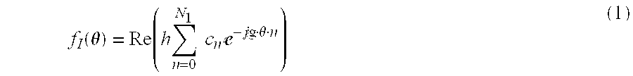
- f I ( ⁇ ) The equation for f I ( ⁇ ) can be considered the sum of a number of simpler equations.
- N 1 is an integer
- h is a size scaling term
- c n is a complex coefficient for the k th term, which coefficient may be ⁇ 1 ⁇
- g is a shape scaling term
- j ⁇ square root over ( ⁇ 1) ⁇ .
- the parameters are chosen such that the function does not have a cusp for any value of ⁇ between 0 and ⁇ , and does not have multiple values for any value of ⁇ between 0 and ⁇ . In graphical terms this means that the line formed by the equation f I ( ⁇ ) (i.e., the circumference of the driven element) cannot have any points or hooks.
- the equation for f O ( ⁇ ) (i.e., the inner circumference of the cutout portion of the ground element) is determined by adding the width of the tapered clearance area at a given angle to the equation f I ( ⁇ ). Since the width of the tapered clearance area W TCA is never zero, but is always some minimum width, the width of the tapered clearance area W TCA for a given angle ⁇ is determined as follows:
- ⁇ is a constant that defines the minimum width of the tapered clearance area at the feed point
- N 2 and N 3 are integers
- ⁇ is a first shape scaling term
- d is a second shape scaling term
- a n is a complex coefficient for the n th term, which coefficient maybe ⁇ 1 ⁇
- ⁇ 1, and j ⁇ square root over ( ⁇ 1) ⁇ .
- Equation f I ( ⁇ ) and f I ( ⁇ ) are preferably symmetric around the line formed at the angles of 0 and ⁇ . If they are not and are only useful between 0 and ⁇ , then the following symmetry equations can supply the other half:
- the slopes of f I ( ⁇ ) and f O ( ⁇ ) are zero with respect to the origin. Since the functions f I ( ⁇ ) and f O ( ⁇ ) are symmetric around the line that travels from 0 to ⁇ , this means that there will be no discontinuity where the two halves of f I ( ⁇ ) and f O ( ⁇ ) meet. Rather, the two halves will meet at either end along contiguous lines.
- the antennas shown in FIGS. 1-22 can be formed by any way that provides the desired layers and elements within the layers.
- a preferred method of fabrication involves the use of boards that comprise an insulating material with two layers of conductive material on either side. During fabrication the two conductive layers are etched as needed to provide the desired circuit layers, and any vias are made in the insulating material of the boards. Then the two boards are sealed together, e.g., using an insulating glue.
- FIG. 23 shows the E-plane and H-plane beam pattern shapes of the antenna of FIG. 1 .
- the pattern in both planes is similar to the E-plane pattern of a dipole, with nulls at the sides and the main beams 2301 orthogonal to the nulls.
- the main beams 2301 are perpendicular to the plane of the antenna 100 .
- the radiation nulls lie in the plane of the substrate. This characteristic advantageously permits arraying of the antenna 100 with low element-to-element mutual interaction.
- the disclosed antenna illustrated in FIGS. 1-22 shows that an extremely high performance UWB antenna, transmitter, and receive front end system can be integrated onto a low-cost PC board.
- the various embodiments of the present invention provide an electrically small planar UWB antenna that can be arrayed on a single substrate.
- the UWB antenna includes a tapered, “doughnut” shape clearance area within a sheet of conductive material (e.g., copper), in which the feed is across the clearance area.
- a ground element has a cutout section that is defined by the outer edge of the clearance area.
- a driven element which is situated in the clearance area, is defined by the inner edge of the clearance area.
- the clearance area width is tapered to increase as a function of the distance from the feed point.
- the clearance area width, as well as the shape of the driven element, has an axis of symmetry about the feed point.
- the antenna can be fed by connecting a transmission line to the feed point such that the shield (or ground) of the transmission line is connected to the ground at the edge of the clearance area, and the center conductor of the transmission line is connected to the driven element also at the edge of the clearance area.
Abstract
Description

Claims (28)
Priority Applications (2)
| Application Number | Priority Date | Filing Date | Title |
|---|---|---|---|
| US10/054,790 US6590545B2 (en) | 2000-08-07 | 2002-01-25 | Electrically small planar UWB antenna apparatus and related system |
| US10/601,308 US6914573B1 (en) | 2000-08-07 | 2003-06-23 | Electrically small planar UWB antenna apparatus and related system |
Applications Claiming Priority (2)
| Application Number | Priority Date | Filing Date | Title |
|---|---|---|---|
| US63381500A | 2000-08-07 | 2000-08-07 | |
| US10/054,790 US6590545B2 (en) | 2000-08-07 | 2002-01-25 | Electrically small planar UWB antenna apparatus and related system |
Related Parent Applications (1)
| Application Number | Title | Priority Date | Filing Date |
|---|---|---|---|
| US63381500A Continuation-In-Part | 2000-08-07 | 2000-08-07 |
Related Child Applications (1)
| Application Number | Title | Priority Date | Filing Date |
|---|---|---|---|
| US10/601,308 Continuation US6914573B1 (en) | 2000-08-07 | 2003-06-23 | Electrically small planar UWB antenna apparatus and related system |
Publications (2)
| Publication Number | Publication Date |
|---|---|
| US20020122010A1 US20020122010A1 (en) | 2002-09-05 |
| US6590545B2 true US6590545B2 (en) | 2003-07-08 |
Family
ID=24541229
Family Applications (1)
| Application Number | Title | Priority Date | Filing Date |
|---|---|---|---|
| US10/054,790 Expired - Fee Related US6590545B2 (en) | 2000-08-07 | 2002-01-25 | Electrically small planar UWB antenna apparatus and related system |
Country Status (3)
| Country | Link |
|---|---|
| US (1) | US6590545B2 (en) |
| AU (1) | AU2001282867A1 (en) |
| WO (1) | WO2002013313A2 (en) |
Cited By (29)
| Publication number | Priority date | Publication date | Assignee | Title |
|---|---|---|---|---|
| US20040100408A1 (en) * | 2002-11-27 | 2004-05-27 | Taiyo Yuden Co., Ltd. | Wide bandwidth antenna |
| US20050042999A1 (en) * | 2003-08-22 | 2005-02-24 | Rappaport Theodore S. | Broadband repeater with security for ultrawideband technologies |
| US20050078042A1 (en) * | 2003-09-22 | 2005-04-14 | Thales Plc | Antenna |
| US20050110687A1 (en) * | 2003-11-21 | 2005-05-26 | Starkie Timothy J.S. | Ultrawideband antenna |
| US20050151693A1 (en) * | 2003-10-20 | 2005-07-14 | Next-Rf, Inc. | Spectral control antenna apparatus and method |
| US20050280580A1 (en) * | 2004-06-21 | 2005-12-22 | Ding-Fu Lin | Ultra wide band planar monopole trapezoidal antenna |
| US20060028388A1 (en) * | 2002-12-16 | 2006-02-09 | Schantz Hans G | Chiral polarization ultrawideband slot antenna |
| US20060119529A1 (en) * | 2004-12-03 | 2006-06-08 | Dragan Krupezevic | Ultra wideband antenna |
| US20060232487A1 (en) * | 2005-04-18 | 2006-10-19 | Universal Scientific Industrial Co., Ltd. | Antenna device having ultra wide bandwidth characteristics |
| WO2006115363A1 (en) | 2005-04-26 | 2006-11-02 | E.M.W. Antenna Co., Ltd. | Ultra-wideband antenna having a band notch characteristic |
| US20070069955A1 (en) * | 2005-09-29 | 2007-03-29 | Freescale Semiconductor, Inc. | Frequency-notching antenna |
| US20070075405A1 (en) * | 2005-09-30 | 2007-04-05 | Xiaoning Ye | System and method to control signal line capacitance |
| US20070085743A1 (en) * | 2005-10-18 | 2007-04-19 | Paul Eberhardt | Antenna system and apparatus |
| US20070109195A1 (en) * | 2005-11-16 | 2007-05-17 | Universal Scientific Industrial Co., Ltd. | Ultra wide bandwidth planar antenna |
| US20070241982A1 (en) * | 2004-09-30 | 2007-10-18 | Alan Stigliani | Contoured triangular dipole antenna |
| US20080094299A1 (en) * | 2006-07-07 | 2008-04-24 | Iti Scotland Limited | Antenna arrangement |
| US20090184880A1 (en) * | 2008-01-17 | 2009-07-23 | Eric Marklein | Ultra Wideband Loop Antenna |
| US20100019979A1 (en) * | 2008-07-25 | 2010-01-28 | The United States of America as represented by the the Attorney General | Tulip antenna with tuning stub |
| US20100045532A1 (en) * | 2005-06-20 | 2010-02-25 | E.M.W. Antenna Co., Ltd. | Antenna using electrically conductive ink and production method thereof |
| US20100256462A1 (en) * | 2007-09-05 | 2010-10-07 | Sensible Medical Innovations Ltd. | Method and system for monitoring thoracic tissue fluid |
| US20110025295A1 (en) * | 2009-07-30 | 2011-02-03 | Sensible Medical Innovations Ltd. | System and method for calibration of measurements of interacted em signals in real time |
| US8489162B1 (en) * | 2010-08-17 | 2013-07-16 | Amazon Technologies, Inc. | Slot antenna within existing device component |
| US20140292595A1 (en) * | 2013-03-29 | 2014-10-02 | Samsung Electronics Co., Ltd. | Antenna device and electronic device including the antenna device |
| US20160191109A1 (en) * | 2014-12-24 | 2016-06-30 | Lg Innotek Co., Ltd. | Single pole double throw switch |
| US9572511B2 (en) | 2007-09-05 | 2017-02-21 | Sensible Medical Innovations Ltd. | Methods and systems for monitoring intrabody tissues |
| US20170324142A1 (en) * | 2016-05-06 | 2017-11-09 | GM Global Technology Operations LLC | Wideband transparent elliptical antenna applique for attachment to glass |
| US10667715B2 (en) | 2008-08-20 | 2020-06-02 | Sensible Medical Innovations Ltd. | Methods and devices of cardiac tissue monitoring and analysis |
| US11095035B2 (en) | 2019-02-14 | 2021-08-17 | Aeroantenna Technology, Inc. | Broad band dipole antenna |
| US11277711B2 (en) | 2019-06-19 | 2022-03-15 | Samsung Electronics Co., Ltd. | Electronic device for determining location information of external device |
Families Citing this family (32)
| Publication number | Priority date | Publication date | Assignee | Title |
|---|---|---|---|---|
| JP4170828B2 (en) * | 2002-11-27 | 2008-10-22 | 太陽誘電株式会社 | Antenna and dielectric substrate for antenna |
| JP2004328694A (en) * | 2002-11-27 | 2004-11-18 | Taiyo Yuden Co Ltd | Antenna and wireless communication card |
| JP2004328693A (en) * | 2002-11-27 | 2004-11-18 | Taiyo Yuden Co Ltd | Antenna and dielectric substrate for antenna |
| US7187329B2 (en) * | 2002-11-27 | 2007-03-06 | Taiyo Yuden Co., Ltd. | Antenna, dielectric substrate for antenna, and wireless communication card |
| KR20050010549A (en) * | 2003-07-21 | 2005-01-28 | 엘지전자 주식회사 | minimum size antenna for UWB communication |
| US7187330B2 (en) | 2004-06-22 | 2007-03-06 | Massachusetts Institute Of Technology | Differential and single ended elliptical antennas |
| EP1615294A1 (en) * | 2004-07-02 | 2006-01-11 | Motorola, Inc. | Ultra wide band antenna |
| WO2006054951A1 (en) * | 2004-11-22 | 2006-05-26 | Agency For Science, Technology And Research | Antennas for ultra-wideband applications |
| JP2006186969A (en) * | 2004-12-01 | 2006-07-13 | Omron Corp | Antenna |
| US7683789B2 (en) * | 2005-03-04 | 2010-03-23 | Intelleflex Corporation | Compact omni-directional RF system |
| US20060208898A1 (en) * | 2005-03-04 | 2006-09-21 | Intelleflex Corporation | Compact omnidirectional RF system |
| CN100369323C (en) * | 2005-03-10 | 2008-02-13 | 上海大学 | Super broad band ladder-shape floor printing single pole antenna |
| DE102005034966B4 (en) * | 2005-07-22 | 2013-10-17 | Universität Kassel | Ultra broadband antenna |
| GB2439110B (en) * | 2006-06-13 | 2009-08-19 | Thales Holdings Uk Plc | An ultra wideband antenna |
| US7453402B2 (en) * | 2006-06-19 | 2008-11-18 | Hong Kong Applied Science And Research Institute Co., Ltd. | Miniature balanced antenna with differential feed |
| US7535431B2 (en) * | 2006-09-28 | 2009-05-19 | Hong Kong Applied Science And Technology Research Institute Co., Ltd. | Antenna systems with ground plane extensions and method for use thereof |
| KR20100064391A (en) * | 2007-10-04 | 2010-06-14 | 콸콤 인코포레이티드 | Antenna having a defined gab between first and second radiating elements |
| EP2068400A1 (en) * | 2007-12-03 | 2009-06-10 | Sony Corporation | Slot antenna for mm-wave signals |
| WO2010095175A1 (en) * | 2009-02-19 | 2010-08-26 | 新興産業株式會社 | Antenna |
| CN101916913A (en) * | 2010-07-26 | 2010-12-15 | 天津职业技术师范大学 | Ultra-wide band microstrip patch antenna |
| US9203456B2 (en) * | 2012-09-25 | 2015-12-01 | Htc Corporation | Mobile device |
| CN103915682A (en) * | 2013-01-06 | 2014-07-09 | 华为技术有限公司 | Printed circuit board antenna and printed circuit board |
| CN103618136A (en) * | 2013-11-07 | 2014-03-05 | 中国计量学院 | Ring-encircled wideband coplanar antenna |
| JP6345529B2 (en) * | 2014-08-01 | 2018-06-20 | スタッフ株式会社 | Antenna device for ultra-wideband communication |
| US9735475B2 (en) | 2014-12-01 | 2017-08-15 | Anderson Contract Engineering, Inc. | Low cost antenna array and methods of manufacture |
| US10530036B2 (en) | 2016-05-06 | 2020-01-07 | Gm Global Technology Operations, Llc | Dualband flexible antenna with segmented surface treatment |
| US10396427B2 (en) * | 2016-05-06 | 2019-08-27 | GM Global Technology Operations LLC | Dual polarized wideband LTE thin film antenna |
| TWI617097B (en) * | 2016-05-10 | 2018-03-01 | S-ring resonant monopole antenna | |
| CN107039729A (en) * | 2017-03-18 | 2017-08-11 | 深圳市景程信息科技有限公司 | Metal ground structure in wideband balun |
| CN107069204B (en) * | 2017-04-21 | 2023-06-13 | 吉林医药学院 | Elliptic gap ultra-wideband planar gap antenna with stepped structure |
| WO2021148051A1 (en) * | 2020-01-20 | 2021-07-29 | 展讯通信(上海)有限公司 | Broadband external antenna and wireless communication device |
| TWI764682B (en) * | 2021-04-22 | 2022-05-11 | 和碩聯合科技股份有限公司 | Antenna module |
Citations (132)
| Publication number | Priority date | Publication date | Assignee | Title |
|---|---|---|---|---|
| US2239724A (en) * | 1938-05-18 | 1941-04-29 | Rca Corp | Wide band antenna |
| US2454766A (en) * | 1943-04-24 | 1948-11-30 | Standard Telephones Cables Ltd | Broad band antenna |
| US2671896A (en) | 1942-12-18 | 1954-03-09 | Itt | Random impulse system |
| US2999128A (en) | 1945-11-14 | 1961-09-05 | Conrad H Hoeppner | Pulse communication system |
| US3364491A (en) * | 1958-12-10 | 1968-01-16 | Siemens Ag | Broadband ellipsoidal dipole antenna |
| US3587107A (en) | 1969-06-11 | 1971-06-22 | Sperry Rand Corp | Time limited impulse response antenna |
| US3612899A (en) | 1970-08-20 | 1971-10-12 | Sperry Rand Corp | Generator for short-duration high-frequency pulse signals |
| US3659203A (en) | 1970-06-15 | 1972-04-25 | Sperry Rand Corp | Balanced radiator system |
| US3662316A (en) | 1971-03-12 | 1972-05-09 | Sperry Rand Corp | Short base-band pulse receiver |
| US3668639A (en) | 1971-05-07 | 1972-06-06 | Itt | Sequency filters based on walsh functions for signals with three space variables |
| US3678204A (en) | 1970-10-26 | 1972-07-18 | Itt | Signal processing and transmission by means of walsh functions |
| US3705981A (en) | 1970-10-05 | 1972-12-12 | Itt | Sequency filters based on walsh functions for signals with two space variables |
| US3728632A (en) | 1971-03-12 | 1973-04-17 | Sperry Rand Corp | Transmission and reception system for generating and receiving base-band pulse duration pulse signals without distortion for short base-band communication system |
| US3739392A (en) | 1971-07-29 | 1973-06-12 | Sperry Rand Corp | Base-band radiation and reception system |
| US3772697A (en) | 1971-04-19 | 1973-11-13 | Sperry Rand Corp | Base-band pulse object sensor system |
| US3794996A (en) | 1972-07-12 | 1974-02-26 | Sperry Rand Corp | Stable base-band superregenerative selective receiver |
| US3806795A (en) | 1972-01-03 | 1974-04-23 | Geophysical Survey Sys Inc | Geophysical surveying system employing electromagnetic impulses |
| US3878749A (en) | 1972-12-12 | 1975-04-22 | Allen Organ Co | Walsh function tone generator and system |
| US3934252A (en) | 1974-04-08 | 1976-01-20 | Sperry Rand Corporation | Closed loop tunnel diode receiver for operation with a base band semiconductor transmitter |
| US3995212A (en) | 1975-04-14 | 1976-11-30 | Sperry Rand Corporation | Apparatus and method for sensing a liquid with a single wire transmission line |
| US4017854A (en) | 1975-08-21 | 1977-04-12 | Sperry Rand Corporation | Apparatus for angular measurement and beam forming with baseband radar systems |
| US4063246A (en) * | 1976-06-01 | 1977-12-13 | Transco Products, Inc. | Coplanar stripline antenna |
| US4072942A (en) | 1976-02-20 | 1978-02-07 | Calspan Corporation | Apparatus for the detection of buried objects |
| US4099118A (en) | 1977-07-25 | 1978-07-04 | Franklin Robert C | Electronic wall stud sensor |
| US4152701A (en) | 1978-04-20 | 1979-05-01 | Sperry Rand Corporation | Base band speed sensor |
| US4254418A (en) | 1978-08-23 | 1981-03-03 | Sperry Corporation | Collision avoidance system using short pulse signal reflectometry |
| US4344705A (en) | 1979-03-07 | 1982-08-17 | Endress U. Hauser Gmbh U. Co. | Distance measuring apparatus based on the pulse travel time method |
| US4473906A (en) | 1980-12-05 | 1984-09-25 | Lord Corporation | Active acoustic attenuator |
| US4506267A (en) | 1983-01-26 | 1985-03-19 | Geophysical Survey Systems, Inc. | Frequency independent shielded loop antenna |
| US4641317A (en) | 1984-12-03 | 1987-02-03 | Charles A. Phillips | Spread spectrum radio transmission system |
| US4651152A (en) | 1983-09-26 | 1987-03-17 | Geophysical Survey Systems, Inc. | Large relative bandwidth radar |
| US4688041A (en) | 1981-10-08 | 1987-08-18 | Sperry Corporation | Baseband detector with anti-jam capability |
| US4695752A (en) | 1982-01-11 | 1987-09-22 | Sperry Corporation | Narrow range gate baseband receiver |
| US4698633A (en) | 1982-05-19 | 1987-10-06 | Sperry Corporation | Antennas for wide bandwidth signals |
| US4743906A (en) | 1984-12-03 | 1988-05-10 | Charles A. Phillips | Time domain radio transmission system |
| US4751515A (en) | 1980-07-09 | 1988-06-14 | Corum James F | Electromagnetic structure and method |
| US4813057A (en) | 1984-12-03 | 1989-03-14 | Charles A. Phillips | Time domain radio transmission system |
| US4862174A (en) | 1986-11-19 | 1989-08-29 | Natio Yoshiyuki | Electromagnetic wave absorber |
| US4907001A (en) | 1987-08-21 | 1990-03-06 | Geophysical Survey Systems, Inc. | Extraction of radar targets from clutter |
| US5057846A (en) | 1990-03-26 | 1991-10-15 | Geophysical Survey Systems, Inc. | Efficient operation of probing radar in absorbing media |
| US5090024A (en) | 1989-08-23 | 1992-02-18 | Intellon Corporation | Spread spectrum communications system for networks |
| US5095312A (en) | 1991-04-12 | 1992-03-10 | The United States Of America As Represented By The Secretary Of The Navy | Impulse transmitter and quantum detection radar system |
| US5134408A (en) | 1991-01-30 | 1992-07-28 | Geophysical Survey Systems, Inc. | Detection of radar signals with large radar signatures |
| US5146616A (en) | 1991-06-27 | 1992-09-08 | Hughes Aircraft Company | Ultra wideband radar transmitter employing synthesized short pulses |
| US5148174A (en) | 1991-02-13 | 1992-09-15 | Geophysical Survey Systems, Inc. | Selective reception of carrier-free radar signals with large relative bandwidth |
| US5153595A (en) | 1990-03-26 | 1992-10-06 | Geophysical Survey Systems, Inc. | Range information from signal distortions |
| US5159343A (en) | 1990-03-26 | 1992-10-27 | Geophysical Survey Systems, Inc. | Range information from signal distortions |
| US5177486A (en) | 1991-11-25 | 1993-01-05 | The United States Of America As Represented By The Secretary Of The Army | Optically activated hybrid pulser with patterned radiating element |
| US5216695A (en) | 1991-06-14 | 1993-06-01 | Anro Engineering, Inc. | Short pulse microwave source with a high prf and low power drain |
| US5216429A (en) | 1991-04-17 | 1993-06-01 | Ricoh Company, Ltd. | Position measuring system using pseudo-noise signal transmission and reception |
| US5223838A (en) | 1992-04-07 | 1993-06-29 | Hughes Aircraft Company | Radar cross section enhancement using phase conjugated impulse signals |
| US5227621A (en) | 1992-09-18 | 1993-07-13 | The United States Of America As Represented By The Secretary Of The Army | Ultra-wideband high power photon triggered frequency independent radiator |
| US5237586A (en) | 1992-03-25 | 1993-08-17 | Ericsson-Ge Mobile Communications Holding, Inc. | Rake receiver with selective ray combining |
| US5239309A (en) | 1991-06-27 | 1993-08-24 | Hughes Aircraft Company | Ultra wideband radar employing synthesized short pulses |
| US5248975A (en) | 1991-06-26 | 1993-09-28 | Geophysical Survey Systems, Inc. | Ground probing radar with multiple antenna capability |
| US5274271A (en) | 1991-07-12 | 1993-12-28 | Regents Of The University Of California | Ultra-short pulse generator |
| US5307081A (en) | 1990-11-27 | 1994-04-26 | Geophysical Survey Systems, Inc. | Radiator for slowly varying electromagnetic waves |
| US5313056A (en) | 1993-08-06 | 1994-05-17 | The United States Of America As Represented By The Secretary Of The Army | Electronically controlled frequency agile impulse device |
| US5319218A (en) | 1993-05-06 | 1994-06-07 | The United States Of America As Represented By The Secretary Of The Army | Pulse sharpening using an optical pulse |
| US5323169A (en) | 1993-01-11 | 1994-06-21 | Voss Scientific | Compact, high-gain, ultra-wide band (UWB) transverse electromagnetic (TEM) planar transmission-line-array horn antenna |
| US5332938A (en) | 1992-04-06 | 1994-07-26 | Regents Of The University Of California | High voltage MOSFET switching circuit |
| US5337054A (en) | 1992-05-18 | 1994-08-09 | Anro Engineering, Inc. | Coherent processing tunnel diode ultra wideband receiver |
| US5345471A (en) | 1993-04-12 | 1994-09-06 | The Regents Of The University Of California | Ultra-wideband receiver |
| US5351053A (en) | 1993-07-30 | 1994-09-27 | The United States Of America As Represented By The Secretary Of The Air Force | Ultra wideband radar signal processor for electronically scanned arrays |
| US5353301A (en) | 1993-09-17 | 1994-10-04 | Motorola, Inc. | Method and apparatus for combining multipath spread-spectrum signals |
| US5352974A (en) | 1992-08-14 | 1994-10-04 | Zircon Corporation | Stud sensor with digital averager and dual sensitivity |
| US5359624A (en) | 1993-06-07 | 1994-10-25 | Motorola, Inc. | System and method for chip timing synchronization in an adaptive direct sequence CDMA communication system |
| US5361070A (en) | 1993-04-12 | 1994-11-01 | Regents Of The University Of California | Ultra-wideband radar motion sensor |
| US5363108A (en) | 1984-12-03 | 1994-11-08 | Charles A. Phillips | Time domain radio transmission system |
| US5365240A (en) | 1992-11-04 | 1994-11-15 | Geophysical Survey Systems, Inc. | Efficient driving circuit for large-current radiator |
| US5377225A (en) | 1993-10-19 | 1994-12-27 | Hughes Aircraft Company | Multiple-access noise rejection filter for a DS-CDMA system |
| US5381151A (en) | 1994-02-02 | 1995-01-10 | Grumman Aerospace Corporation | Signal processing for ultra-wideband impulse radar |
| US5389939A (en) | 1993-03-31 | 1995-02-14 | Hughes Aircraft Company | Ultra wideband phased array antenna |
| US5394163A (en) * | 1992-08-26 | 1995-02-28 | Hughes Missile Systems Company | Annular slot patch excited array |
| US5422607A (en) | 1994-02-09 | 1995-06-06 | The Regents Of The University Of California | Linear phase compressive filter |
| US5426618A (en) | 1993-05-03 | 1995-06-20 | Chen; Hong-Bin | Method of high resolution and high SNR data acquisition for probing using pulse-compression |
| US5455593A (en) | 1994-07-18 | 1995-10-03 | Anro Engineering, Inc. | Efficiently decreasing the bandwidth and increasing the radiated energy of an UWB radar or data link transmission |
| US5457394A (en) | 1993-04-12 | 1995-10-10 | The Regents Of The University Of California | Impulse radar studfinder |
| US5465100A (en) * | 1991-02-01 | 1995-11-07 | Alcatel N.V. | Radiating device for a plannar antenna |
| US5465094A (en) | 1994-01-14 | 1995-11-07 | The Regents Of The University Of California | Two terminal micropower radar sensor |
| US5471162A (en) | 1992-09-08 | 1995-11-28 | The Regents Of The University Of California | High speed transient sampler |
| US5486833A (en) | 1993-04-02 | 1996-01-23 | Barrett; Terence W. | Active signalling systems |
| US5493691A (en) | 1993-12-23 | 1996-02-20 | Barrett; Terence W. | Oscillator-shuttle-circuit (OSC) networks for conditioning energy in higher-order symmetry algebraic topological forms and RF phase conjugation |
| US5495499A (en) | 1990-11-28 | 1996-02-27 | Novatel Communications, Ltd. | Pseudorandom noise ranging receiver which compensates for multipath distortion by dynamically adjusting the time delay spacing between early and late correlators |
| US5506592A (en) * | 1992-05-29 | 1996-04-09 | Texas Instruments Incorporated | Multi-octave, low profile, full instantaneous azimuthal field of view direction finding antenna |
| US5510800A (en) | 1993-04-12 | 1996-04-23 | The Regents Of The University Of California | Time-of-flight radio location system |
| US5517198A (en) | 1993-04-12 | 1996-05-14 | The Regents Of The University Of California | Ultra-wideband directional sampler |
| US5519400A (en) | 1993-04-12 | 1996-05-21 | The Regents Of The University Of California | Phase coded, micro-power impulse radar motion sensor |
| US5521600A (en) | 1994-09-06 | 1996-05-28 | The Regents Of The University Of California | Range-gated field disturbance sensor with range-sensitivity compensation |
| US5523760A (en) | 1993-04-12 | 1996-06-04 | The Regents Of The University Of California | Ultra-wideband receiver |
| US5523758A (en) | 1990-01-25 | 1996-06-04 | Geophysical Survey Systems, Inc. | Sliding correlator for nanosecond pulses |
| US5526299A (en) | 1990-05-18 | 1996-06-11 | Yale University | Method and apparatus for encoding and decoding using wavelet-packets |
| US5533046A (en) | 1992-10-08 | 1996-07-02 | Lund; Vanmetre | Spread spectrum communication system |
| US5543799A (en) | 1994-09-02 | 1996-08-06 | Zircon Corporation | Swept range gate radar system for detection of nearby objects |
| US5563605A (en) | 1995-08-02 | 1996-10-08 | The Regents Of The University Of California | Precision digital pulse phase generator |
| US5568522A (en) | 1995-03-20 | 1996-10-22 | General Electric Company | Correction of multipath distortion in wideband carrier signals |
| US5573012A (en) | 1994-08-09 | 1996-11-12 | The Regents Of The University Of California | Body monitoring and imaging apparatus and method |
| US5576627A (en) | 1994-09-06 | 1996-11-19 | The Regents Of The University Of California | Narrow field electromagnetic sensor system and method |
| US5581256A (en) | 1994-09-06 | 1996-12-03 | The Regents Of The University Of California | Range gated strip proximity sensor |
| US5586145A (en) | 1993-01-11 | 1996-12-17 | Morgan; Harry C. | Transmission of electronic information by pulse position modulation utilizing low average power |
| US5589838A (en) | 1994-09-06 | 1996-12-31 | The Regents Of The University Of California | Short range radio locator system |
| US5592177A (en) | 1993-06-11 | 1997-01-07 | Autometric, Incorporated | Polarization-rotation modulated, spread polarization-rotation, wide-bandwidth radio-wave communications system |
| US5594456A (en) | 1994-09-07 | 1997-01-14 | Patriot Scientific Corporation | Gas tube RF antenna |
| US5596601A (en) | 1994-08-30 | 1997-01-21 | Lucent Technologies Inc. | Method and apparatus for spread spectrum code pulse position modulation |
| US5602964A (en) | 1993-05-21 | 1997-02-11 | Autometric, Incorporated | Automata networks and methods for obtaining optimized dynamically reconfigurable computational architectures and controls |
| US5609059A (en) | 1994-12-19 | 1997-03-11 | The Regents Of The University Of California | Electronic multi-purpose material level sensor |
| US5610611A (en) | 1994-12-19 | 1997-03-11 | The Regents Of The University Of California | High accuracy electronic material level sensor |
| US5610907A (en) | 1994-07-29 | 1997-03-11 | Barrett; Terence W. | Ultrafast time hopping CDMA-RF communications: code-as-carrier, multichannel operation, high data rate operation and data rate on demand |
| US5623511A (en) | 1994-08-30 | 1997-04-22 | Lucent Technologies Inc. | Spread spectrum code pulse position modulated receiver having delay spread compensation |
| US5627856A (en) | 1994-09-09 | 1997-05-06 | Omnipoint Corporation | Method and apparatus for receiving and despreading a continuous phase-modulated spread spectrum signal using self-synchronizing correlators |
| US5630216A (en) | 1994-09-06 | 1997-05-13 | The Regents Of The University Of California | Micropower RF transponder with superregenerative receiver and RF receiver with sampling mixer |
| US5640419A (en) | 1994-07-19 | 1997-06-17 | Grumman Aerospace Corporation | Covert communication system |
| US5648787A (en) | 1994-11-29 | 1997-07-15 | Patriot Scientific Corporation | Penetrating microwave radar ground plane antenna |
| US5654978A (en) | 1993-11-01 | 1997-08-05 | Omnipoint Corporation | Pulse position modulation with spread spectrum |
| US5659572A (en) | 1993-11-22 | 1997-08-19 | Interdigital Technology Corporation | Phased array spread spectrum system and method |
| US5661490A (en) | 1993-04-12 | 1997-08-26 | The Regents Of The University Of California | Time-of-flight radio location system |
| US5661385A (en) | 1994-12-19 | 1997-08-26 | The Regents Of The University Of California | Window-closing safety system |
| US5663889A (en) | 1993-12-28 | 1997-09-02 | Fujitsu Limited | Apparatus for computing delay time of integrated circuit |
| US5673050A (en) | 1996-06-14 | 1997-09-30 | Moussally; George | Three-dimensional underground imaging radar system |
| US5673286A (en) | 1995-01-04 | 1997-09-30 | Interdigital Technology Corporation | Spread spectrum multipath processor system and method |
| US5677927A (en) | 1994-09-20 | 1997-10-14 | Pulson Communications Corporation | Ultrawide-band communication system and method |
| US5682164A (en) | 1994-09-06 | 1997-10-28 | The Regents Of The University Of California | Pulse homodyne field disturbance sensor |
| US5687169A (en) | 1995-04-27 | 1997-11-11 | Time Domain Systems, Inc. | Full duplex ultrawide-band communication system and method |
| US5748891A (en) | 1994-07-22 | 1998-05-05 | Aether Wire & Location | Spread spectrum localizers |
| US5872545A (en) * | 1996-01-03 | 1999-02-16 | Agence Spatiale Europeene | Planar microwave receive and/or transmit array antenna and application thereof to reception from geostationary television satellites |
| US5898408A (en) * | 1995-10-25 | 1999-04-27 | Larsen Electronics, Inc. | Window mounted mobile antenna system using annular ring aperture coupling |
| US5956624A (en) | 1994-07-12 | 1999-09-21 | Usa Digital Radio Partners Lp | Method and system for simultaneously broadcasting and receiving digital and analog signals |
| US6144344A (en) * | 1997-12-10 | 2000-11-07 | Samsung Electronics Co., Ltd. | Antenna apparatus for base station |
| US6198437B1 (en) * | 1998-07-09 | 2001-03-06 | The United States Of America As Represented By The Secretary Of The Air Force | Broadband patch/slot antenna |
| US6278410B1 (en) | 1999-11-29 | 2001-08-21 | Interuniversitair Microelektronica Centrum | Wide frequency band planar antenna |
| US6300908B1 (en) | 1998-09-09 | 2001-10-09 | Centre National De La Recherche Scientifique (Cnrs) | Antenna |
| US6351256B1 (en) * | 1997-08-29 | 2002-02-26 | Sharp Kabushiki Kaisha | Addressing method and apparatus |
-
2001
- 2001-07-31 WO PCT/US2001/021125 patent/WO2002013313A2/en active Application Filing
- 2001-07-31 AU AU2001282867A patent/AU2001282867A1/en not_active Abandoned
-
2002
- 2002-01-25 US US10/054,790 patent/US6590545B2/en not_active Expired - Fee Related
Patent Citations (138)
| Publication number | Priority date | Publication date | Assignee | Title |
|---|---|---|---|---|
| US2239724A (en) * | 1938-05-18 | 1941-04-29 | Rca Corp | Wide band antenna |
| US2671896A (en) | 1942-12-18 | 1954-03-09 | Itt | Random impulse system |
| US2454766A (en) * | 1943-04-24 | 1948-11-30 | Standard Telephones Cables Ltd | Broad band antenna |
| US2999128A (en) | 1945-11-14 | 1961-09-05 | Conrad H Hoeppner | Pulse communication system |
| US3364491A (en) * | 1958-12-10 | 1968-01-16 | Siemens Ag | Broadband ellipsoidal dipole antenna |
| US3587107A (en) | 1969-06-11 | 1971-06-22 | Sperry Rand Corp | Time limited impulse response antenna |
| US3659203A (en) | 1970-06-15 | 1972-04-25 | Sperry Rand Corp | Balanced radiator system |
| US3612899A (en) | 1970-08-20 | 1971-10-12 | Sperry Rand Corp | Generator for short-duration high-frequency pulse signals |
| US3705981A (en) | 1970-10-05 | 1972-12-12 | Itt | Sequency filters based on walsh functions for signals with two space variables |
| US3678204A (en) | 1970-10-26 | 1972-07-18 | Itt | Signal processing and transmission by means of walsh functions |
| US3662316A (en) | 1971-03-12 | 1972-05-09 | Sperry Rand Corp | Short base-band pulse receiver |
| US3728632A (en) | 1971-03-12 | 1973-04-17 | Sperry Rand Corp | Transmission and reception system for generating and receiving base-band pulse duration pulse signals without distortion for short base-band communication system |
| US3772697A (en) | 1971-04-19 | 1973-11-13 | Sperry Rand Corp | Base-band pulse object sensor system |
| US3668639A (en) | 1971-05-07 | 1972-06-06 | Itt | Sequency filters based on walsh functions for signals with three space variables |
| US3739392A (en) | 1971-07-29 | 1973-06-12 | Sperry Rand Corp | Base-band radiation and reception system |
| US3806795A (en) | 1972-01-03 | 1974-04-23 | Geophysical Survey Sys Inc | Geophysical surveying system employing electromagnetic impulses |
| US3794996A (en) | 1972-07-12 | 1974-02-26 | Sperry Rand Corp | Stable base-band superregenerative selective receiver |
| US3878749A (en) | 1972-12-12 | 1975-04-22 | Allen Organ Co | Walsh function tone generator and system |
| US3934252A (en) | 1974-04-08 | 1976-01-20 | Sperry Rand Corporation | Closed loop tunnel diode receiver for operation with a base band semiconductor transmitter |
| US3995212A (en) | 1975-04-14 | 1976-11-30 | Sperry Rand Corporation | Apparatus and method for sensing a liquid with a single wire transmission line |
| US4017854A (en) | 1975-08-21 | 1977-04-12 | Sperry Rand Corporation | Apparatus for angular measurement and beam forming with baseband radar systems |
| US4072942A (en) | 1976-02-20 | 1978-02-07 | Calspan Corporation | Apparatus for the detection of buried objects |
| US4063246A (en) * | 1976-06-01 | 1977-12-13 | Transco Products, Inc. | Coplanar stripline antenna |
| US4099118A (en) | 1977-07-25 | 1978-07-04 | Franklin Robert C | Electronic wall stud sensor |
| US4152701A (en) | 1978-04-20 | 1979-05-01 | Sperry Rand Corporation | Base band speed sensor |
| US4254418A (en) | 1978-08-23 | 1981-03-03 | Sperry Corporation | Collision avoidance system using short pulse signal reflectometry |
| US4344705A (en) | 1979-03-07 | 1982-08-17 | Endress U. Hauser Gmbh U. Co. | Distance measuring apparatus based on the pulse travel time method |
| US4751515A (en) | 1980-07-09 | 1988-06-14 | Corum James F | Electromagnetic structure and method |
| US4473906A (en) | 1980-12-05 | 1984-09-25 | Lord Corporation | Active acoustic attenuator |
| US4688041A (en) | 1981-10-08 | 1987-08-18 | Sperry Corporation | Baseband detector with anti-jam capability |
| US4695752A (en) | 1982-01-11 | 1987-09-22 | Sperry Corporation | Narrow range gate baseband receiver |
| US4698633A (en) | 1982-05-19 | 1987-10-06 | Sperry Corporation | Antennas for wide bandwidth signals |
| US4506267A (en) | 1983-01-26 | 1985-03-19 | Geophysical Survey Systems, Inc. | Frequency independent shielded loop antenna |
| US4651152A (en) | 1983-09-26 | 1987-03-17 | Geophysical Survey Systems, Inc. | Large relative bandwidth radar |
| US4641317A (en) | 1984-12-03 | 1987-02-03 | Charles A. Phillips | Spread spectrum radio transmission system |
| US4743906A (en) | 1984-12-03 | 1988-05-10 | Charles A. Phillips | Time domain radio transmission system |
| US4813057A (en) | 1984-12-03 | 1989-03-14 | Charles A. Phillips | Time domain radio transmission system |
| US5363108A (en) | 1984-12-03 | 1994-11-08 | Charles A. Phillips | Time domain radio transmission system |
| US4979186A (en) | 1984-12-03 | 1990-12-18 | Charles A. Phillips | Time domain radio transmission system |
| US4862174A (en) | 1986-11-19 | 1989-08-29 | Natio Yoshiyuki | Electromagnetic wave absorber |
| US4907001A (en) | 1987-08-21 | 1990-03-06 | Geophysical Survey Systems, Inc. | Extraction of radar targets from clutter |
| US5090024A (en) | 1989-08-23 | 1992-02-18 | Intellon Corporation | Spread spectrum communications system for networks |
| US5523758A (en) | 1990-01-25 | 1996-06-04 | Geophysical Survey Systems, Inc. | Sliding correlator for nanosecond pulses |
| US5153595A (en) | 1990-03-26 | 1992-10-06 | Geophysical Survey Systems, Inc. | Range information from signal distortions |
| US5159343A (en) | 1990-03-26 | 1992-10-27 | Geophysical Survey Systems, Inc. | Range information from signal distortions |
| US5057846A (en) | 1990-03-26 | 1991-10-15 | Geophysical Survey Systems, Inc. | Efficient operation of probing radar in absorbing media |
| US5526299A (en) | 1990-05-18 | 1996-06-11 | Yale University | Method and apparatus for encoding and decoding using wavelet-packets |
| US5307081A (en) | 1990-11-27 | 1994-04-26 | Geophysical Survey Systems, Inc. | Radiator for slowly varying electromagnetic waves |
| US5495499A (en) | 1990-11-28 | 1996-02-27 | Novatel Communications, Ltd. | Pseudorandom noise ranging receiver which compensates for multipath distortion by dynamically adjusting the time delay spacing between early and late correlators |
| US5134408A (en) | 1991-01-30 | 1992-07-28 | Geophysical Survey Systems, Inc. | Detection of radar signals with large radar signatures |
| US5465100A (en) * | 1991-02-01 | 1995-11-07 | Alcatel N.V. | Radiating device for a plannar antenna |
| US5148174A (en) | 1991-02-13 | 1992-09-15 | Geophysical Survey Systems, Inc. | Selective reception of carrier-free radar signals with large relative bandwidth |
| US5095312A (en) | 1991-04-12 | 1992-03-10 | The United States Of America As Represented By The Secretary Of The Navy | Impulse transmitter and quantum detection radar system |
| US5216429A (en) | 1991-04-17 | 1993-06-01 | Ricoh Company, Ltd. | Position measuring system using pseudo-noise signal transmission and reception |
| US5307079A (en) | 1991-06-14 | 1994-04-26 | Anro Engineering, Inc. | Short pulse microwave source with a high PRF and low power drain |
| US5216695A (en) | 1991-06-14 | 1993-06-01 | Anro Engineering, Inc. | Short pulse microwave source with a high prf and low power drain |
| US5248975A (en) | 1991-06-26 | 1993-09-28 | Geophysical Survey Systems, Inc. | Ground probing radar with multiple antenna capability |
| US5239309A (en) | 1991-06-27 | 1993-08-24 | Hughes Aircraft Company | Ultra wideband radar employing synthesized short pulses |
| US5146616A (en) | 1991-06-27 | 1992-09-08 | Hughes Aircraft Company | Ultra wideband radar transmitter employing synthesized short pulses |
| US5274271A (en) | 1991-07-12 | 1993-12-28 | Regents Of The University Of California | Ultra-short pulse generator |
| US5177486A (en) | 1991-11-25 | 1993-01-05 | The United States Of America As Represented By The Secretary Of The Army | Optically activated hybrid pulser with patterned radiating element |
| US5237586A (en) | 1992-03-25 | 1993-08-17 | Ericsson-Ge Mobile Communications Holding, Inc. | Rake receiver with selective ray combining |
| US5332938A (en) | 1992-04-06 | 1994-07-26 | Regents Of The University Of California | High voltage MOSFET switching circuit |
| US5223838A (en) | 1992-04-07 | 1993-06-29 | Hughes Aircraft Company | Radar cross section enhancement using phase conjugated impulse signals |
| US5337054A (en) | 1992-05-18 | 1994-08-09 | Anro Engineering, Inc. | Coherent processing tunnel diode ultra wideband receiver |
| US5506592A (en) * | 1992-05-29 | 1996-04-09 | Texas Instruments Incorporated | Multi-octave, low profile, full instantaneous azimuthal field of view direction finding antenna |
| US5352974A (en) | 1992-08-14 | 1994-10-04 | Zircon Corporation | Stud sensor with digital averager and dual sensitivity |
| US5394163A (en) * | 1992-08-26 | 1995-02-28 | Hughes Missile Systems Company | Annular slot patch excited array |
| US5519342A (en) | 1992-09-08 | 1996-05-21 | The Regents Of The University Of California | Transient digitizer with displacement current samplers |
| US5471162A (en) | 1992-09-08 | 1995-11-28 | The Regents Of The University Of California | High speed transient sampler |
| US5479120A (en) | 1992-09-08 | 1995-12-26 | The Regents Of The University Of California | High speed sampler and demultiplexer |
| US5227621A (en) | 1992-09-18 | 1993-07-13 | The United States Of America As Represented By The Secretary Of The Army | Ultra-wideband high power photon triggered frequency independent radiator |
| US5533046A (en) | 1992-10-08 | 1996-07-02 | Lund; Vanmetre | Spread spectrum communication system |
| US5365240A (en) | 1992-11-04 | 1994-11-15 | Geophysical Survey Systems, Inc. | Efficient driving circuit for large-current radiator |
| US5586145A (en) | 1993-01-11 | 1996-12-17 | Morgan; Harry C. | Transmission of electronic information by pulse position modulation utilizing low average power |
| US5323169A (en) | 1993-01-11 | 1994-06-21 | Voss Scientific | Compact, high-gain, ultra-wide band (UWB) transverse electromagnetic (TEM) planar transmission-line-array horn antenna |
| US5389939A (en) | 1993-03-31 | 1995-02-14 | Hughes Aircraft Company | Ultra wideband phased array antenna |
| US5486833A (en) | 1993-04-02 | 1996-01-23 | Barrett; Terence W. | Active signalling systems |
| US5361070A (en) | 1993-04-12 | 1994-11-01 | Regents Of The University Of California | Ultra-wideband radar motion sensor |
| US5517198A (en) | 1993-04-12 | 1996-05-14 | The Regents Of The University Of California | Ultra-wideband directional sampler |
| US5361070B1 (en) | 1993-04-12 | 2000-05-16 | Univ California | Ultra-wideband radar motion sensor |
| US5457394A (en) | 1993-04-12 | 1995-10-10 | The Regents Of The University Of California | Impulse radar studfinder |
| US5661490A (en) | 1993-04-12 | 1997-08-26 | The Regents Of The University Of California | Time-of-flight radio location system |
| US5345471A (en) | 1993-04-12 | 1994-09-06 | The Regents Of The University Of California | Ultra-wideband receiver |
| US5523760A (en) | 1993-04-12 | 1996-06-04 | The Regents Of The University Of California | Ultra-wideband receiver |
| US5519400A (en) | 1993-04-12 | 1996-05-21 | The Regents Of The University Of California | Phase coded, micro-power impulse radar motion sensor |
| US5510800A (en) | 1993-04-12 | 1996-04-23 | The Regents Of The University Of California | Time-of-flight radio location system |
| US5426618A (en) | 1993-05-03 | 1995-06-20 | Chen; Hong-Bin | Method of high resolution and high SNR data acquisition for probing using pulse-compression |
| US5319218A (en) | 1993-05-06 | 1994-06-07 | The United States Of America As Represented By The Secretary Of The Army | Pulse sharpening using an optical pulse |
| US5512834A (en) | 1993-05-07 | 1996-04-30 | The Regents Of The University Of California | Homodyne impulse radar hidden object locator |
| US5602964A (en) | 1993-05-21 | 1997-02-11 | Autometric, Incorporated | Automata networks and methods for obtaining optimized dynamically reconfigurable computational architectures and controls |
| US5359624A (en) | 1993-06-07 | 1994-10-25 | Motorola, Inc. | System and method for chip timing synchronization in an adaptive direct sequence CDMA communication system |
| US5592177A (en) | 1993-06-11 | 1997-01-07 | Autometric, Incorporated | Polarization-rotation modulated, spread polarization-rotation, wide-bandwidth radio-wave communications system |
| US5351053A (en) | 1993-07-30 | 1994-09-27 | The United States Of America As Represented By The Secretary Of The Air Force | Ultra wideband radar signal processor for electronically scanned arrays |
| US5313056A (en) | 1993-08-06 | 1994-05-17 | The United States Of America As Represented By The Secretary Of The Army | Electronically controlled frequency agile impulse device |
| US5353301A (en) | 1993-09-17 | 1994-10-04 | Motorola, Inc. | Method and apparatus for combining multipath spread-spectrum signals |
| US5377225A (en) | 1993-10-19 | 1994-12-27 | Hughes Aircraft Company | Multiple-access noise rejection filter for a DS-CDMA system |
| US5654978A (en) | 1993-11-01 | 1997-08-05 | Omnipoint Corporation | Pulse position modulation with spread spectrum |
| US5659572A (en) | 1993-11-22 | 1997-08-19 | Interdigital Technology Corporation | Phased array spread spectrum system and method |
| US5493691A (en) | 1993-12-23 | 1996-02-20 | Barrett; Terence W. | Oscillator-shuttle-circuit (OSC) networks for conditioning energy in higher-order symmetry algebraic topological forms and RF phase conjugation |
| US5663889A (en) | 1993-12-28 | 1997-09-02 | Fujitsu Limited | Apparatus for computing delay time of integrated circuit |
| US5465094A (en) | 1994-01-14 | 1995-11-07 | The Regents Of The University Of California | Two terminal micropower radar sensor |
| US5381151A (en) | 1994-02-02 | 1995-01-10 | Grumman Aerospace Corporation | Signal processing for ultra-wideband impulse radar |
| US5422607A (en) | 1994-02-09 | 1995-06-06 | The Regents Of The University Of California | Linear phase compressive filter |
| US5956624A (en) | 1994-07-12 | 1999-09-21 | Usa Digital Radio Partners Lp | Method and system for simultaneously broadcasting and receiving digital and analog signals |
| US5455593A (en) | 1994-07-18 | 1995-10-03 | Anro Engineering, Inc. | Efficiently decreasing the bandwidth and increasing the radiated energy of an UWB radar or data link transmission |
| US5640419A (en) | 1994-07-19 | 1997-06-17 | Grumman Aerospace Corporation | Covert communication system |
| US5748891A (en) | 1994-07-22 | 1998-05-05 | Aether Wire & Location | Spread spectrum localizers |
| US5610907A (en) | 1994-07-29 | 1997-03-11 | Barrett; Terence W. | Ultrafast time hopping CDMA-RF communications: code-as-carrier, multichannel operation, high data rate operation and data rate on demand |
| US5573012A (en) | 1994-08-09 | 1996-11-12 | The Regents Of The University Of California | Body monitoring and imaging apparatus and method |
| US5623511A (en) | 1994-08-30 | 1997-04-22 | Lucent Technologies Inc. | Spread spectrum code pulse position modulated receiver having delay spread compensation |
| US5596601A (en) | 1994-08-30 | 1997-01-21 | Lucent Technologies Inc. | Method and apparatus for spread spectrum code pulse position modulation |
| US5543799A (en) | 1994-09-02 | 1996-08-06 | Zircon Corporation | Swept range gate radar system for detection of nearby objects |
| US5589838A (en) | 1994-09-06 | 1996-12-31 | The Regents Of The University Of California | Short range radio locator system |
| US5581256A (en) | 1994-09-06 | 1996-12-03 | The Regents Of The University Of California | Range gated strip proximity sensor |
| US5630216A (en) | 1994-09-06 | 1997-05-13 | The Regents Of The University Of California | Micropower RF transponder with superregenerative receiver and RF receiver with sampling mixer |
| US5521600A (en) | 1994-09-06 | 1996-05-28 | The Regents Of The University Of California | Range-gated field disturbance sensor with range-sensitivity compensation |
| US5576627A (en) | 1994-09-06 | 1996-11-19 | The Regents Of The University Of California | Narrow field electromagnetic sensor system and method |
| US5682164A (en) | 1994-09-06 | 1997-10-28 | The Regents Of The University Of California | Pulse homodyne field disturbance sensor |
| US5594456A (en) | 1994-09-07 | 1997-01-14 | Patriot Scientific Corporation | Gas tube RF antenna |
| US5627856A (en) | 1994-09-09 | 1997-05-06 | Omnipoint Corporation | Method and apparatus for receiving and despreading a continuous phase-modulated spread spectrum signal using self-synchronizing correlators |
| US5677927A (en) | 1994-09-20 | 1997-10-14 | Pulson Communications Corporation | Ultrawide-band communication system and method |
| US5648787A (en) | 1994-11-29 | 1997-07-15 | Patriot Scientific Corporation | Penetrating microwave radar ground plane antenna |
| US5609059A (en) | 1994-12-19 | 1997-03-11 | The Regents Of The University Of California | Electronic multi-purpose material level sensor |
| US5661385A (en) | 1994-12-19 | 1997-08-26 | The Regents Of The University Of California | Window-closing safety system |
| US5610611A (en) | 1994-12-19 | 1997-03-11 | The Regents Of The University Of California | High accuracy electronic material level sensor |
| US5673286A (en) | 1995-01-04 | 1997-09-30 | Interdigital Technology Corporation | Spread spectrum multipath processor system and method |
| US5568522A (en) | 1995-03-20 | 1996-10-22 | General Electric Company | Correction of multipath distortion in wideband carrier signals |
| US5687169A (en) | 1995-04-27 | 1997-11-11 | Time Domain Systems, Inc. | Full duplex ultrawide-band communication system and method |
| US5563605A (en) | 1995-08-02 | 1996-10-08 | The Regents Of The University Of California | Precision digital pulse phase generator |
| US5898408A (en) * | 1995-10-25 | 1999-04-27 | Larsen Electronics, Inc. | Window mounted mobile antenna system using annular ring aperture coupling |
| US5872545A (en) * | 1996-01-03 | 1999-02-16 | Agence Spatiale Europeene | Planar microwave receive and/or transmit array antenna and application thereof to reception from geostationary television satellites |
| US5673050A (en) | 1996-06-14 | 1997-09-30 | Moussally; George | Three-dimensional underground imaging radar system |
| US6351256B1 (en) * | 1997-08-29 | 2002-02-26 | Sharp Kabushiki Kaisha | Addressing method and apparatus |
| US6144344A (en) * | 1997-12-10 | 2000-11-07 | Samsung Electronics Co., Ltd. | Antenna apparatus for base station |
| US6198437B1 (en) * | 1998-07-09 | 2001-03-06 | The United States Of America As Represented By The Secretary Of The Air Force | Broadband patch/slot antenna |
| US6300908B1 (en) | 1998-09-09 | 2001-10-09 | Centre National De La Recherche Scientifique (Cnrs) | Antenna |
| US6278410B1 (en) | 1999-11-29 | 2001-08-21 | Interuniversitair Microelektronica Centrum | Wide frequency band planar antenna |
Non-Patent Citations (6)
| Title |
|---|
| Chen Q et al: "Time-Domain Diakoptics Active Slot-Ring Antena Analysis Using FDTD", Proceedings of the 26th European Microwave Conference 1996. Prague, Sep. 9-13, 1996, Proceedings of the European Microwave Conference, Swnley, Nexus Media, GB, vol. 1 conf. 26, Sep. 9, 1996, pp. 440-443, XP000876059 ISBN:1-899919-08-2. |
| Low-Power, Miniature, Distributed Position Location And Communication Devices Using Ultra-Wideband, Nonsinusoidal Communication Technology, Advanced Research Projects Agancy/Federal Bureau of Investigation, Jul. 1995, pp. 1-40. |
| Radar Technology May Held Improve Automobile Safety, Tuesday's Newsline, Tuesday, Mar. 29, 1994, vol. 19, No. 22. |
| Single-Shot Transient Digitizer (1993), Inventor Thomas McEwan Motion Detector Technology, Inventor Thomas McEwan. |
| Soliman E A et al: "Coplanar versus slotline mode in exciting CPW-fed planar atennas", 29th European Microwave Conference 99. Incorporating MIOP '99. Conference Proceedings, Proceedings of 29th European Microwave Conference, Munich, Germany, Oct. 5-7, 1999, pp. 150-153 vol. 3, XP002187453 1999, London, UK, Microwave Eng. Eur, UK ISBN: 0-86213-152-9. |
| World's Fastest Solid-State Digitizer, Energy & Technology Review, Apr., 1994, McEwan et al., pp. 1-6. |
Cited By (68)
| Publication number | Priority date | Publication date | Assignee | Title |
|---|---|---|---|---|
| US20040100408A1 (en) * | 2002-11-27 | 2004-05-27 | Taiyo Yuden Co., Ltd. | Wide bandwidth antenna |
| US7075483B2 (en) * | 2002-11-27 | 2006-07-11 | Taiyo Yuden Co., Ltd. | Wide bandwidth antenna |
| US20060028388A1 (en) * | 2002-12-16 | 2006-02-09 | Schantz Hans G | Chiral polarization ultrawideband slot antenna |
| US7391383B2 (en) * | 2002-12-16 | 2008-06-24 | Next-Rf, Inc. | Chiral polarization ultrawideband slot antenna |
| US7676194B2 (en) | 2003-08-22 | 2010-03-09 | Rappaport Theodore S | Broadband repeater with security for ultrawideband technologies |
| US8600295B2 (en) | 2003-08-22 | 2013-12-03 | Theodore S. Rappaport | Networking method with broadband relay |
| US20050042999A1 (en) * | 2003-08-22 | 2005-02-24 | Rappaport Theodore S. | Broadband repeater with security for ultrawideband technologies |
| US10224999B2 (en) | 2003-08-22 | 2019-03-05 | Theodore S. Rappaport | Broadband repeater with security for ultrawideband technologies |
| US9667337B2 (en) | 2003-08-22 | 2017-05-30 | Theodore S. Rappaport | Intelligent broadband relay for wireless networks for connectivity to mobile or portable devices |
| US10797783B2 (en) | 2003-08-22 | 2020-10-06 | Theodore S. Rappaport | Broadband repeater with security for ultrawideband technologies |
| US9722690B2 (en) | 2003-08-22 | 2017-08-01 | Theodore S. Rappaport | Network and networking method with intelligent broadband wireless relay for connectivity to mobile or portable devices |
| US8611812B2 (en) | 2003-08-22 | 2013-12-17 | Theodore S. Rappaport | Broadband wireless relay |
| US20100120361A1 (en) * | 2003-08-22 | 2010-05-13 | Rappaport Theodore S | Broadband Repeater with Security for Ultrawideband Technologies |
| US8331854B2 (en) | 2003-08-22 | 2012-12-11 | Rappaport Theodore S | Broadband repeater with security for ultrawideband technologies |
| US7983613B2 (en) | 2003-08-22 | 2011-07-19 | Rappaport Theodore S | Broadband repeater with security for ultrawideband technologies |
| US8918049B2 (en) | 2003-08-22 | 2014-12-23 | Theodore S. Rappaport | Network with intelligent broadband wireless relay |
| US8923754B2 (en) | 2003-08-22 | 2014-12-30 | Theodore S. Rappaport | Intelligent broadband relay for wireless networks |
| US20050078042A1 (en) * | 2003-09-22 | 2005-04-14 | Thales Plc | Antenna |
| US7239283B2 (en) * | 2003-09-22 | 2007-07-03 | Thales Plc | Antenna |
| US7064723B2 (en) | 2003-10-20 | 2006-06-20 | Next-Rf, Inc. | Spectral control antenna apparatus and method |
| US20050151693A1 (en) * | 2003-10-20 | 2005-07-14 | Next-Rf, Inc. | Spectral control antenna apparatus and method |
| US7327315B2 (en) * | 2003-11-21 | 2008-02-05 | Artimi Ltd. | Ultrawideband antenna |
| US20050110687A1 (en) * | 2003-11-21 | 2005-05-26 | Starkie Timothy J.S. | Ultrawideband antenna |
| US20050280580A1 (en) * | 2004-06-21 | 2005-12-22 | Ding-Fu Lin | Ultra wide band planar monopole trapezoidal antenna |
| US20070241982A1 (en) * | 2004-09-30 | 2007-10-18 | Alan Stigliani | Contoured triangular dipole antenna |
| US7262741B2 (en) * | 2004-12-03 | 2007-08-28 | Sony Deutschland Gmbh | Ultra wideband antenna |
| US20060119529A1 (en) * | 2004-12-03 | 2006-06-08 | Dragan Krupezevic | Ultra wideband antenna |
| US7170451B2 (en) | 2005-04-18 | 2007-01-30 | Universal Scientific Industrial Co., Ltd. | Antenna device having ultra wide bandwidth characteristics |
| US20060232487A1 (en) * | 2005-04-18 | 2006-10-19 | Universal Scientific Industrial Co., Ltd. | Antenna device having ultra wide bandwidth characteristics |
| US20100182210A1 (en) * | 2005-04-26 | 2010-07-22 | Byung-Hoon Ryou | Ultra-wideband antenna having a band notch characteristic |
| WO2006115363A1 (en) | 2005-04-26 | 2006-11-02 | E.M.W. Antenna Co., Ltd. | Ultra-wideband antenna having a band notch characteristic |
| US8115681B2 (en) | 2005-04-26 | 2012-02-14 | Emw Co., Ltd. | Ultra-wideband antenna having a band notch characteristic |
| US20100045532A1 (en) * | 2005-06-20 | 2010-02-25 | E.M.W. Antenna Co., Ltd. | Antenna using electrically conductive ink and production method thereof |
| US8106830B2 (en) | 2005-06-20 | 2012-01-31 | Emw Co., Ltd. | Antenna using electrically conductive ink and production method thereof |
| US7352333B2 (en) * | 2005-09-29 | 2008-04-01 | Freescale Semiconductor, Inc. | Frequency-notching antenna |
| US20070069955A1 (en) * | 2005-09-29 | 2007-03-29 | Freescale Semiconductor, Inc. | Frequency-notching antenna |
| US20070075405A1 (en) * | 2005-09-30 | 2007-04-05 | Xiaoning Ye | System and method to control signal line capacitance |
| US7361994B2 (en) * | 2005-09-30 | 2008-04-22 | Intel Corporation | System to control signal line capacitance |
| US7358901B2 (en) | 2005-10-18 | 2008-04-15 | Pulse-Link, Inc. | Antenna system and apparatus |
| US20070085743A1 (en) * | 2005-10-18 | 2007-04-19 | Paul Eberhardt | Antenna system and apparatus |
| US20070109195A1 (en) * | 2005-11-16 | 2007-05-17 | Universal Scientific Industrial Co., Ltd. | Ultra wide bandwidth planar antenna |
| US7307588B2 (en) * | 2005-11-16 | 2007-12-11 | Universal Scientific Industrial Co., Ltd. | Ultra wide bandwidth planar antenna |
| US7898492B2 (en) * | 2006-07-07 | 2011-03-01 | Iti Scotland Limited | Antenna arrangement |
| US20080094299A1 (en) * | 2006-07-07 | 2008-04-24 | Iti Scotland Limited | Antenna arrangement |
| US20100256462A1 (en) * | 2007-09-05 | 2010-10-07 | Sensible Medical Innovations Ltd. | Method and system for monitoring thoracic tissue fluid |
| US11564586B2 (en) | 2007-09-05 | 2023-01-31 | Sensible Medical Innovations Ltd. | Method and system for monitoring thoracic tissue fluid |
| US20110160549A1 (en) * | 2007-09-05 | 2011-06-30 | Saroka Amir | Method, system and apparatus for using electromagnetic radiation for monitoring a tissue of a user |
| US10758150B2 (en) | 2007-09-05 | 2020-09-01 | Sensible Medical lnnovations Ltd. | Method, system and apparatus for using electromagnetic radiation for monitoring a tissue of a user |
| US11944419B2 (en) | 2007-09-05 | 2024-04-02 | Sensible Medical Innovations Ltd. | Method and system for monitoring thoracic tissue fluid |
| US10561336B2 (en) | 2007-09-05 | 2020-02-18 | Sensible Medical Innovations Ltd. | Method and system for monitoring thoracic tissue fluid |
| US9572511B2 (en) | 2007-09-05 | 2017-02-21 | Sensible Medical Innovations Ltd. | Methods and systems for monitoring intrabody tissues |
| US10506943B2 (en) | 2007-09-05 | 2019-12-17 | Sensible Medical Innovations Ltd. | Methods and systems for monitoring intrabody tissues |
| US7639201B2 (en) | 2008-01-17 | 2009-12-29 | University Of Massachusetts | Ultra wideband loop antenna |
| US20090184880A1 (en) * | 2008-01-17 | 2009-07-23 | Eric Marklein | Ultra Wideband Loop Antenna |
| US7791554B2 (en) | 2008-07-25 | 2010-09-07 | The United States Of America As Represented By The Attorney General | Tulip antenna with tuning stub |
| US20100019979A1 (en) * | 2008-07-25 | 2010-01-28 | The United States of America as represented by the the Attorney General | Tulip antenna with tuning stub |
| US11529065B2 (en) | 2008-08-20 | 2022-12-20 | Sensible Medical Innovations Ltd. | Methods and devices of cardiac tissue monitoring and analysis |
| US10667715B2 (en) | 2008-08-20 | 2020-06-02 | Sensible Medical Innovations Ltd. | Methods and devices of cardiac tissue monitoring and analysis |
| US20110025295A1 (en) * | 2009-07-30 | 2011-02-03 | Sensible Medical Innovations Ltd. | System and method for calibration of measurements of interacted em signals in real time |
| US8907682B2 (en) | 2009-07-30 | 2014-12-09 | Sensible Medical Innovations Ltd. | System and method for calibration of measurements of interacted EM signals in real time |
| US8489162B1 (en) * | 2010-08-17 | 2013-07-16 | Amazon Technologies, Inc. | Slot antenna within existing device component |
| US9293829B2 (en) * | 2013-03-29 | 2016-03-22 | Samsung Electronics Co., Ltd | Antenna device and electronic device including the antenna device |
| US20140292595A1 (en) * | 2013-03-29 | 2014-10-02 | Samsung Electronics Co., Ltd. | Antenna device and electronic device including the antenna device |
| US20160191109A1 (en) * | 2014-12-24 | 2016-06-30 | Lg Innotek Co., Ltd. | Single pole double throw switch |
| US20170324142A1 (en) * | 2016-05-06 | 2017-11-09 | GM Global Technology Operations LLC | Wideband transparent elliptical antenna applique for attachment to glass |
| US10707554B2 (en) * | 2016-05-06 | 2020-07-07 | GM Global Technology Operations LLC | Wideband transparent elliptical antenna applique for attachment to glass |
| US11095035B2 (en) | 2019-02-14 | 2021-08-17 | Aeroantenna Technology, Inc. | Broad band dipole antenna |
| US11277711B2 (en) | 2019-06-19 | 2022-03-15 | Samsung Electronics Co., Ltd. | Electronic device for determining location information of external device |
Also Published As
| Publication number | Publication date |
|---|---|
| WO2002013313A2 (en) | 2002-02-14 |
| US20020122010A1 (en) | 2002-09-05 |
| WO2002013313A3 (en) | 2003-01-03 |
| AU2001282867A1 (en) | 2002-02-18 |
Similar Documents
| Publication | Publication Date | Title |
|---|---|---|
| US6590545B2 (en) | Electrically small planar UWB antenna apparatus and related system | |
| US6914573B1 (en) | Electrically small planar UWB antenna apparatus and related system | |
| US7324049B2 (en) | Miniaturized ultra-wideband microstrip antenna | |
| EP1279202B1 (en) | Planar ultra wide band antenna with integrated electronics | |
| US6292153B1 (en) | Antenna comprising two wideband notch regions on one coplanar substrate | |
| US6246377B1 (en) | Antenna comprising two separate wideband notch regions on one coplanar substrate | |
| US8395552B2 (en) | Antenna module having reduced size, high gain, and increased power efficiency | |
| US7589686B2 (en) | Small ultra wideband antenna having unidirectional radiation pattern | |
| US6281843B1 (en) | Planar broadband dipole antenna for linearly polarized waves | |
| US4843403A (en) | Broadband notch antenna | |
| JP4390651B2 (en) | Antenna for UWB (Ultra-WideBand) communication | |
| US7271776B2 (en) | Device for the reception and/or the transmission of multibeam signals | |
| WO1997025755A1 (en) | Slot spiral antenna with integrated balun and feed | |
| US11258171B2 (en) | Antenna | |
| NZ272910A (en) | Multiple beam antenna: simultaneous circular and linear polarisation signalling | |
| Wójcik et al. | High port-to-port isolation dual-polarized antenna array dedicated for full-duplex base stations | |
| US6335710B1 (en) | Tuneable spiral antenna | |
| KR100535255B1 (en) | Small planar antenna with ultra wide bandwidth and manufacturing method thereof | |
| WO2019223318A1 (en) | Indoor base station and pifa antenna thereof | |
| GB2453778A (en) | An ultra wideband antenna with a high impedance surface reflector | |
| US4987423A (en) | Wide band loop antenna with disymmetrical feeding, notably antenna for transmission, and array antenna formed by several such antennas | |
| KR100449857B1 (en) | Wideband Printed Dipole Antenna | |
| Mozharovskiy et al. | Dual-Polarized Integrated Lens Antenna for Outdoor 60 GHz Point-to-Point Systems | |
| CN218569225U (en) | Ultra-wideband antenna and communication equipment | |
| US20230420858A1 (en) | End-fire tapered slot antenna |
Legal Events
| Date | Code | Title | Description |
|---|---|---|---|
| AS | Assignment |
Owner name: XTREMESPECTRUM, INC., VIRGINIA Free format text: ASSIGNMENT OF ASSIGNORS INTEREST;ASSIGNOR:MCCORKLE, JOHN W.;REEL/FRAME:012576/0105 Effective date: 20020125 |
|
| AS | Assignment |
Owner name: GRANITE VENTURES, LLC, CALIFORNIA Free format text: SECURITY INTEREST;ASSIGNOR:XTREMESPECTRUM, INC.;REEL/FRAME:013452/0732 Effective date: 20030228 Owner name: SILICON VALLEY BANK, MASSACHUSETTS Free format text: SECURITY INTEREST;ASSIGNOR:XTREME SPECTRUM, INC.;REEL/FRAME:013452/0597 Effective date: 20030228 |
|
| AS | Assignment |
Owner name: XTREMESPECTRUM, INC., VIRGINIA Free format text: TERMINATION OF SECURITY AGREEMENT;ASSIGNOR:GRANITE VENTURES, LLC;REEL/FRAME:014141/0449 Effective date: 20031110 |
|
| AS | Assignment |
Owner name: MOTOROLA, INC., ILLINOIS Free format text: ASSIGNMENT OF ASSIGNORS INTEREST;ASSIGNOR:XTREMESPECTRUM, INC.;REEL/FRAME:014815/0242 Effective date: 20031113 Owner name: MOTOROLA, INC.,ILLINOIS Free format text: ASSIGNMENT OF ASSIGNORS INTEREST;ASSIGNOR:XTREMESPECTRUM, INC.;REEL/FRAME:014815/0242 Effective date: 20031113 |
|
| AS | Assignment |
Owner name: FREESCALE SEMICONDUCTOR, INC., TEXAS Free format text: ASSIGNMENT OF ASSIGNORS INTEREST;ASSIGNOR:MOTOROLA, INC.;REEL/FRAME:015698/0657 Effective date: 20040404 Owner name: FREESCALE SEMICONDUCTOR, INC.,TEXAS Free format text: ASSIGNMENT OF ASSIGNORS INTEREST;ASSIGNOR:MOTOROLA, INC.;REEL/FRAME:015698/0657 Effective date: 20040404 |
|
| AS | Assignment |
Owner name: FREESCALE SEMICONDUCTOR, INC., TEXAS Free format text: ASSIGNMENT OF ASSIGNORS INTEREST;ASSIGNOR:MOTOROLA, INC.;REEL/FRAME:015603/0299 Effective date: 20041210 |
|
| AS | Assignment |
Owner name: XTREMESPECTRUM, INC., VIRGINIA Free format text: INTELLECTUAL PROPERTY SECURITY AGREEMENT TERMINATION;ASSIGNOR:SILICON VALLEY BANK;REEL/FRAME:018584/0147 Effective date: 20031120 |
|
| FPAY | Fee payment |
Year of fee payment: 4 |
|
| AS | Assignment |
Owner name: CITIBANK, N.A. AS COLLATERAL AGENT, NEW YORK Free format text: SECURITY AGREEMENT;ASSIGNORS:FREESCALE SEMICONDUCTOR, INC.;FREESCALE ACQUISITION CORPORATION;FREESCALE ACQUISITION HOLDINGS CORP.;AND OTHERS;REEL/FRAME:018855/0129 Effective date: 20061201 Owner name: CITIBANK, N.A. AS COLLATERAL AGENT,NEW YORK Free format text: SECURITY AGREEMENT;ASSIGNORS:FREESCALE SEMICONDUCTOR, INC.;FREESCALE ACQUISITION CORPORATION;FREESCALE ACQUISITION HOLDINGS CORP.;AND OTHERS;REEL/FRAME:018855/0129 Effective date: 20061201 |
|
| AS | Assignment |
Owner name: CITIBANK, N.A., AS COLLATERAL AGENT,NEW YORK Free format text: SECURITY AGREEMENT;ASSIGNOR:FREESCALE SEMICONDUCTOR, INC.;REEL/FRAME:024397/0001 Effective date: 20100413 Owner name: CITIBANK, N.A., AS COLLATERAL AGENT, NEW YORK Free format text: SECURITY AGREEMENT;ASSIGNOR:FREESCALE SEMICONDUCTOR, INC.;REEL/FRAME:024397/0001 Effective date: 20100413 |
|
| REMI | Maintenance fee reminder mailed | ||
| LAPS | Lapse for failure to pay maintenance fees | ||
| STCH | Information on status: patent discontinuation |
Free format text: PATENT EXPIRED DUE TO NONPAYMENT OF MAINTENANCE FEES UNDER 37 CFR 1.362 |
|
| FP | Lapsed due to failure to pay maintenance fee |
Effective date: 20110708 |
|
| AS | Assignment |
Owner name: FREESCALE SEMICONDUCTOR, INC., TEXAS Free format text: PATENT RELEASE;ASSIGNOR:CITIBANK, N.A., AS COLLATERAL AGENT;REEL/FRAME:037354/0225 Effective date: 20151207 Owner name: FREESCALE SEMICONDUCTOR, INC., TEXAS Free format text: PATENT RELEASE;ASSIGNOR:CITIBANK, N.A., AS COLLATERAL AGENT;REEL/FRAME:037356/0553 Effective date: 20151207 Owner name: FREESCALE SEMICONDUCTOR, INC., TEXAS Free format text: PATENT RELEASE;ASSIGNOR:CITIBANK, N.A., AS COLLATERAL AGENT;REEL/FRAME:037356/0143 Effective date: 20151207 |