US6611640B2 - Optical dispersion compensator - Google Patents
Optical dispersion compensator Download PDFInfo
- Publication number
- US6611640B2 US6611640B2 US09/781,984 US78198401A US6611640B2 US 6611640 B2 US6611640 B2 US 6611640B2 US 78198401 A US78198401 A US 78198401A US 6611640 B2 US6611640 B2 US 6611640B2
- Authority
- US
- United States
- Prior art keywords
- optical
- dispersion compensator
- saturable absorber
- peak
- pulse
- Prior art date
- Legal status (The legal status is an assumption and is not a legal conclusion. Google has not performed a legal analysis and makes no representation as to the accuracy of the status listed.)
- Expired - Lifetime
Links
Images


Classifications
-
- G—PHYSICS
- G02—OPTICS
- G02B—OPTICAL ELEMENTS, SYSTEMS OR APPARATUS
- G02B6/00—Light guides; Structural details of arrangements comprising light guides and other optical elements, e.g. couplings
- G02B6/24—Coupling light guides
- G02B6/26—Optical coupling means
- G02B6/28—Optical coupling means having data bus means, i.e. plural waveguides interconnected and providing an inherently bidirectional system by mixing and splitting signals
- G02B6/293—Optical coupling means having data bus means, i.e. plural waveguides interconnected and providing an inherently bidirectional system by mixing and splitting signals with wavelength selective means
- G02B6/29371—Optical coupling means having data bus means, i.e. plural waveguides interconnected and providing an inherently bidirectional system by mixing and splitting signals with wavelength selective means operating principle based on material dispersion
- G02B6/29374—Optical coupling means having data bus means, i.e. plural waveguides interconnected and providing an inherently bidirectional system by mixing and splitting signals with wavelength selective means operating principle based on material dispersion in an optical light guide
- G02B6/29376—Optical coupling means having data bus means, i.e. plural waveguides interconnected and providing an inherently bidirectional system by mixing and splitting signals with wavelength selective means operating principle based on material dispersion in an optical light guide coupling light guides for controlling wavelength dispersion, e.g. by concatenation of two light guides having different dispersion properties
-
- B—PERFORMING OPERATIONS; TRANSPORTING
- B82—NANOTECHNOLOGY
- B82Y—SPECIFIC USES OR APPLICATIONS OF NANOSTRUCTURES; MEASUREMENT OR ANALYSIS OF NANOSTRUCTURES; MANUFACTURE OR TREATMENT OF NANOSTRUCTURES
- B82Y20/00—Nanooptics, e.g. quantum optics or photonic crystals
-
- H—ELECTRICITY
- H04—ELECTRIC COMMUNICATION TECHNIQUE
- H04B—TRANSMISSION
- H04B10/00—Transmission systems employing electromagnetic waves other than radio-waves, e.g. infrared, visible or ultraviolet light, or employing corpuscular radiation, e.g. quantum communication
- H04B10/25—Arrangements specific to fibre transmission
- H04B10/2507—Arrangements specific to fibre transmission for the reduction or elimination of distortion or dispersion
- H04B10/2513—Arrangements specific to fibre transmission for the reduction or elimination of distortion or dispersion due to chromatic dispersion
- H04B10/25133—Arrangements specific to fibre transmission for the reduction or elimination of distortion or dispersion due to chromatic dispersion including a lumped electrical or optical dispersion compensator
-
- H—ELECTRICITY
- H01—ELECTRIC ELEMENTS
- H01S—DEVICES USING THE PROCESS OF LIGHT AMPLIFICATION BY STIMULATED EMISSION OF RADIATION [LASER] TO AMPLIFY OR GENERATE LIGHT; DEVICES USING STIMULATED EMISSION OF ELECTROMAGNETIC RADIATION IN WAVE RANGES OTHER THAN OPTICAL
- H01S3/00—Lasers, i.e. devices using stimulated emission of electromagnetic radiation in the infrared, visible or ultraviolet wave range
- H01S3/05—Construction or shape of optical resonators; Accommodation of active medium therein; Shape of active medium
- H01S3/06—Construction or shape of active medium
- H01S3/063—Waveguide lasers, i.e. whereby the dimensions of the waveguide are of the order of the light wavelength
- H01S3/067—Fibre lasers
- H01S3/06754—Fibre amplifiers
- H01S3/06758—Tandem amplifiers
Definitions
- the present invention is directed to optical communications. More particularly, the present invention is directed to an optical dispersion compensator.
- optical pulse dispersion in an optical communication network causes optical signal pulses to spread out in the time domain.
- Optical pulse dispersion is primarily caused by the differences of the propagation velocity of wavelength components, optical modes, or polarization comprising the optical pulse. Dispersion leads to intersymbol interference in which the optical pulses spread out and overlap one another, thus making it impossible for the detection of the individual pulses. In order to counter the effects of intersymbol interference it is required that the pulses be spaced further apart, which directly limits the possible data rate.
- dispersion shifted fiber that prevents dispersion at a certain wavelength.
- most dispersion shifted fiber is designed with a dispersion zero point around 1550 nm.
- the main drawback with dispersion shifted fiber is that it cannot be used where the fiber has already been installed. Digging up a few hundred kilometers of roadway to replace fiber types is extremely costly. Further, if wavelength division multiplexing (“WDM”) is being used, the problems of four-wave mixing effectively prohibit the use of dispersion shifted fiber.
- WDM wavelength division multiplexing
- Dispersion compensating fiber has its core profile controlled to counteract dispersion. For example, in order to equalize an installed fiber link with dispersion at 1550 nm of 17 ps/nm/km (standard fiber) a shorter length of compensating fiber can be placed in series with it.
- the compensating fiber typically has a dispersion of ⁇ 100 ps/nm/km in the 1550 nm wavelength band. Because the dispersion acts in the opposite direction to the dispersion of the standard fiber the compensating fiber “undisperses” the signal. Therefore, a 100 km length of standard fiber for operation at 1550 nm can be compensated by connecting it to 17 km of compensating fiber.
- Compensating fiber has typical attenuation of 0.5 dB/km.
- the narrow core of dispersion compensating fiber makes it more susceptible to non-linear high power effects than standard fiber and it is also polarization sensitive.
- mid-span spectral inversion One problem with mid-span spectral inversion is that it is difficult to implement in all situations because an active device has to be placed into the middle of the fiber link. This may or may not be practical. In addition, mid-span spectral inversion “undoes” the effect of stimulated Raman scattering in WDM links, thus causing amplification problems.
- Another know method for reducing optical dispersion is the use of chirped Fiber Bragg Gratings.
- a chirped Fiber Bragg Grating the spacing of the lines on the gratings vary continuously over a small range. Shorter wavelength light entering the grating travels along it almost to the end before being reflected. Longer wavelength light is reflected close to the start of the grating. Therefore, short wavelengths are delayed in relation to longer ones. Since the pulse has been dispersed such that short wavelengths arrive before the long ones, the grating can restore the original pulse shape and undo the effects of dispersion.
- chirped Fiber Bragg Gratings need to be quite long. For single-channel application, up to 20 cm is commonly required. In a WDM system a fully continuous chirp would require a very long grating. To compensate for 100 km of standard (17 ps/nm/km) fiber the chirped grating needs to be 17 cm long for every nm of signal bandwidth. Therefore, a WDM system with channels spread over 20 nm would need a chirped Fiber Bragg Grating 340 cm long. Long Fiber Bragg Gratings are very difficult to construct.
- Fiber Bragg Gratings Another problem with chirped Fiber Bragg Gratings is that they have a ripple characteristic in the Group Velocity Dispersion they produce. This ripple can be a source of transmission system noise. The longer the grating the larger the problem with ripple and its resultant noise. In addition, short Fiber Bragg Gratings are filters. When a signal is processed through many stages of filtering, the signal gets very narrow and distorted, and can also have increased noise.
- One embodiment of the present invention is an optical dispersion compensator that includes a saturable absorber. Coupled to the saturable absorber is a pre-amplifier and a post-amplifier.
- FIG. 1 is a perspective view of an optical dispersion compensator in accordance with one embodiment of the present invention.
- FIG. 2 is a graph illustrating a Gaussian shaped optical pulse.
- FIG. 3 is a graph illustrating the relation between optical intensity and absorption coefficient.
- FIG. 4 is a graph illustrating the shape of an input optical pulse and the shape of an optical pulse after the input optical pulse passes through a saturable absorber.
- FIG. 5 illustrates a surface plot of the output intensity of the peak of the optical pulse as a function of I peak /I sat and ⁇ 0 L assuming the background absorption ⁇ b is equal to zero.
- FIG. 6 is a graph illustrating the initial input optical pulse and an output optical pulse after post-amplification.
- FIG. 7 is a graph illustrating the compression ratio vs. ⁇ 0 L for various values of I peak /I sat .
- FIG. 8 is a graph illustrating the compression ratio vs. I peak /I sat for various values of ⁇ 0 L.
- FIG. 9 is a surface plot of the compression ratio vs. ⁇ 0 L and I peak /I sat .
- FIG. 10 is a perspective view of an optical dispersion compensator in accordance with another embodiment of the present invention.
- FIG. 11 is a side view of an optical dispersion compensator in accordance with another embodiment of the present invention.
- FIG. 12 is a side view of an optical dispersion compensator in accordance with another embodiment of the present invention.
- FIG. 13 is a side view of an optical dispersion compensator in accordance with another embodiment of the present invention.
- One embodiment of the present invention is an optical dispersion compensator that includes a saturable absorber.
- the present invention operates independently of the wavelength composition of the optical pulse. Instead, the present invention utilizes the saturable absorber to compress signals based upon the amplitude envelope of the optical pulse.
- FIG. 1 is a perspective view of an optical dispersion compensator in accordance with one embodiment of the present invention.
- Optical dispersion compensator 10 includes saturable absorber material (“SA material”) 25 formed on a substrate 20 as a linear waveguide using conventional thin film processing techniques. Coupled to an input of SA material 25 is an optical pre-amplifier 22 . Coupled to an output of SA material 25 is an optical post-amplifier 24 . The input signal is carried on an input optical fiber 26 coupled to pre-amplifier 22 . The output signal is carried on an output optical fiber 28 coupled to post-amplifier 24 .
- SA material saturated absorber material
- the input signal is a light source carrying optical information in the 1550 or 1300 nm wavelength regions.
- Amplifiers 22 and 24 are rare-earth doped fiber-type amplifiers (e.g., Erbium-doped Fiber Amplifiers (“EDFAs”)), Semiconductor optical amplifiers (“SOAs”) or Raman fiber amplifiers.
- EDFAs Erbium-doped Fiber Amplifiers
- SOAs Semiconductor optical amplifiers
- Raman fiber amplifiers Raman fiber amplifiers.
- Pre-amplifier 22 operates in the linear regime, which is in the unsaturated mode whereby the input optical signal is be amplified but not distorted.
- Post-amplifier 24 also operates in the linear regime.
- SA material 25 has the property that high intensity light is absorbed less than low intensity light. Therefore, SA material 25 acts on an optical signal comprised of a Gaussian shaped pulse by absorbing the tails of the pulse more than the central region, effectively reducing the width of the pulse.
- a saturable absorber such as SA material 25 is a material that displays a reduction in the absorption coefficient at the operational wavelength with increased incident light intensity.
- the behavior of such a material can be modeled as a two state system, i.e., a system possessing two quantum states of different energies that an electron can exist in. In the natural state of the material, one in which no light is incident upon the material, all electrons lie in the lower energy state. An incident photon having a wavelength (hence energy) that corresponds to the energy difference between the quantum states will be absorbed if it excites an electron from the lower energy level to the upper energy level.
- An electron in the upper state will drop back to the lower energy level in one of two ways. It can (1) spontaneously drop back and release energy as heat (referred to as “nonradiative recombination”) or as a photon of the same wavelength that originally excited it (referred to as “spontaneous radiative recombination” or “spontaneous emission”) or (2) interact with another photon, having the wavelength corresponding to the energy difference between quantum states, that forces the electron down to the lower energy level by the release of two photons (referred to as “spontaneous emission”).
- the average time the electron remains in the upper level is given by the relaxation constant ( ⁇ ).
- a saturable absorber such as SA material 25 differs from, for example, a non-linear material.
- a saturable absorber involves the transitions of electrons between quantum states.
- non-linear materials instead of relying on transitions, involve the non-linear reaction due to the electric field of the photons at high photon fluxes (i.e., high light intensity). This reaction is called the electric polarization (P).
- P electric polarization
- optical dispersion compensator 10 can best be explained by describing the action of SA material 25 on input optical signals and optical pulses.
- Input optical signals are typically comprised of a series train in time traveling down input fiber 26 of Gaussian (i.e., bell curved) shaped optical pulses, in which the presence of an optical pulse in a given time slot represents a logical “1” and the lack of an optical pulse in a given time slot represents a logical “0”.
- Gaussian i.e., bell curved
- the representation of the information is dependent upon the coding scheme. This description is of a typical on/off keying code.
- I(t) is the intensity envelope of the optical pulse
- I max is the maximum intensity at the center of the pulse
- t is time
- ⁇ is the standard deviation in units of time.
- FIG. 2 is a graph illustrating a Gaussian shaped optical pulse 40 .
- a saturable absorber such as SA material 25 is an absorbing material in which the absorption coefficient of the material decreases as the intensity of the incident light increases.
- ⁇ 0 is the low field absorption
- ⁇ 0 is the optical cross section
- ⁇ is the relaxation time
- I is the light intensity
- h is Planck's constant
- ⁇ is the incident light frequency
- Eq. 2 illustrates that the intensity dependent absorption coefficient can be improved either by increasing the light intensity of the pulse (I) or by increasing the optical cross section of the saturable absorber material ( ⁇ 0 ).
- the intensity of the input optical signal can be increased by the use of an optical pre-amplifier such as optical pre-amplifier 22 .
- Equally important is the improvement of the saturable absorber material by increasing the optical cross section.
- An increased cross section directly reduces the intensity required for a given level of saturation thus reducing the intensity required of the amplified signal and hence reducing the power demands and cost of the pre-amplifier.
- Eq. 2 can be further simplified by the insertion of the term I sat defined as the intensity at which the absorption coefficient drops to 1 ⁇ 2 its low field value and through the assumption that the response time of the saturable absorber is much less than the rise and fall times of the Gaussian shaped pulse.
- the response times for saturable absorbers can range from less than 1 ps to greater than several hundred picoseconds.
- SA material 25 includes Lead Sulphide quantum dot doped glass and has a typical response time on the order of 2 picoseconds.
- FIG. 3 is a graph illustrating the relation between optical intensity and absorption coefficient.
- I out is the intensity profile of the Gaussian shaped optical pulse after passing through the saturable absorber
- I in is the intensity profile of the Gaussian shaped optical pulse before propagating through the saturable absorber
- L is the length of the saturable absorber medium.
- I out ⁇ ( t ) ( I peak ) ⁇ ⁇ ( - t 2 2 ⁇ ⁇ 2 ) ⁇ ⁇ ( - ⁇ 0 ⁇ L 1 + ( I peak ) ⁇ ⁇ ( - t 2 2 ⁇ ⁇ 2 ) I sat - ⁇ b ⁇ L ) Eq . ⁇ 5
- FIG. 4 is a graph illustrating the shape of an input optical pulse 42 and the shape of an optical pulse 44 after input optical pulse 42 passes through the saturable absorber. Because all of the optical signal (center region and tails) are attenuated in the saturable absorber (although the central region is attenuated less than the tails) an optical post-amplifier such as optical post-amplifier 24 is used to boost the peak of the optical signal back up to point at which it was before passing through the saturable absorber.
- an optical post-amplifier such as optical post-amplifier 24 is used to boost the peak of the optical signal back up to point at which it was before passing through the saturable absorber.
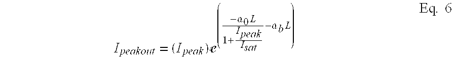
- I peakout ( I peak ) ⁇ ⁇ ( - ⁇ 0 ⁇ L 1 + I peak I sat - ⁇ b ⁇ L ) Eq . ⁇ 6
- FIG. 5 illustrates a surface plot of the output intensity of the peak of the optical pulse as a function of I peak /I sat and ⁇ 0 L assuming the background absorption ⁇ b is equal to zero. If the optical pulse is amplified by the same amount that the peak of the optical pulse was attenuated, Eq.
- I out ⁇ ⁇ ( I peak ) ⁇ ⁇ ⁇ ( - t 2 2 ⁇ ⁇ ⁇ 2 ) ⁇ ⁇ ⁇ ( - ⁇ 0 ⁇ ⁇ L 1 ⁇ + ⁇ ( I peak ) ⁇ ⁇ ⁇ ( - t 2 2 ⁇ ⁇ ⁇ 2 ) I sat ⁇ - ⁇ ⁇ b ⁇ ⁇ L ) ⁇ ⁇ ⁇ ( ⁇ 0 ⁇ ⁇ L 1 ⁇ + ⁇ I peak I sat ) Eq ⁇ . ⁇ 7
- FIG. 6 is a graph illustrating the initial input optical pulse 42 and the output optical pulse 48 after post-amplification.
- the output optical pulse has been compressed compared with the input optical pulse.
- the compression ratio is defined as the factor by which the Full Width Half Maximum (“FWHM”) of the input optical pulse is multiplied by in order to obtain the FWHM of the output pulse.
- the FWHM is defined as the full width of the optical pulse at half the peak of the same pulse.
- FIG. 7 is a graph illustrating the compression ratio vs. ⁇ 0 L for various values of I peak /I sat .
- FIG. 8 is a graph illustrating the compression ratio vs. I peak /I sat for various values of ⁇ 0 L.
- SA material 25 of FIG. 1 is a composite material containing semiconductor nanocrystals (referred to as “quantum dots”) contained in a glass or silicon matrix.
- Quantum dots interspersed within a matrix material offer an opportunity for an ideal saturable absorber for multiple reasons.
- the quantum states of the quantum dots can be engineered to correspond to any wavelength simply by altering their size.
- the density of quantum states i.e., the number of electrons per unit volume that are able to jump from one quantum state to another
- quantum dots eliminate slower excitations that occur at high light intensities such as a two photon absorption that exists in bulk semiconductors. Therefore, the use of quantum dots enables a fast, low power (low intensity), and tunable saturable absorber.
- the quantum dots are comprised of Lead Sulfide, Lead Selenide, Indium Phosphide, Indium Arsenide, etc., and are approximately 5 nanometers in diameter. In a further embodiment, the quantum dots are 5.7 nanometers in diameter. This size of the dots results in a large change of absorption intensity while maintaining fast switching speed.
- the intensity of light required to saturate SA material 25 depends on the size and composition of the dots, as characterized by the optical cross section of SA material 25 .
- the concentration of dots determines how thick a slab of material (quantum dots in glass) is required to produce a given change in intensity of the signal. In one embodiment, a thickness of 0.1 cm is required to arrive at a 20 dB signal change (assuming 50% saturation). Increasing the dot density allows the same change with a thinner device.
- the absorption length ( ⁇ 0 ⁇ 1 ) is related to the optical cross section ( ⁇ 0 )and the number density (dots per volume) of dots N d by:
- the densest packing configuration is the face-centered cubic (“FCC”) lattice which has a packing density of 0.7.
- the quantum dots are produced in a glass matrix.
- the glass matrix material is beneficial because it is transparent to the light which is to be absorbed by the dots, and it acts to confine the electron-hole pairs because it has a much larger band gap than the quantum dot material. This quantum confinement allows the requisite absorption spectrum to be obtained.
- the matrix material is a plastic, or a semiconductor that is transparent to the operational wavelengths.
- matrix materials include Silicate, Borosilicate, and Phosphosilicate glasses, Polymethyl methacrylate (PMMA), Acrylic, polyamine polymers, and semiconductors including Silicon, Silicon Carbide, Cadmium Sulphide, Cadmiun Selenide, Cadmium Telluride, Zinc Sulphide, Aluminum Arsenide, Aluminum Phosphide and Gallium Arsenide.
- PMMA Polymethyl methacrylate
- semiconductors including Silicon, Silicon Carbide, Cadmium Sulphide, Cadmiun Selenide, Cadmium Telluride, Zinc Sulphide, Aluminum Arsenide, Aluminum Phosphide and Gallium Arsenide.
- cladding is added to the quantum dots.
- the purpose of the cladding is to greatly increase the optical cross-section of the core semiconductor quantum dot, thus decreasing the optical power required for saturation as well as decreasing the relaxation time.
- An electrically conducting cladding material (like a metal) locally increases the light intensity within the core semiconductor, thus enhancing the absorption cross section.
- a semiconductor cladding material acts as a surface passivating agent and reduces the number of trapped states, which increases the absorption cross section.
- suitable semiconductor cladding materials include Silicon (Si), Silicon Carbide (SiC), Cadmium Sulfide (CdS), Cadmium Selenide (CdSe), Zinc Sulfide (ZnS), Zinc Selenide (ZnSe), Zinc Telluride (ZnTe), AlAs, AlP, AlSb, GaAs and InP.
- other materials that include metals such as Ag, Au and Al are appropriate for use as cladding materials.
- the thickness of the cladding coating determines the enhancement of the absorption coefficient of the quantum dot material.
- the parameter describing the coating thickness is the ratio of the core radius to the shell radius (“arat”). Typical values of arat are between 0.7 and 0.85. Thus for core radii between 2.5 nm and 5.0 nm (appropriate for PbS), a shell thickness between 0.5 nm and 2.5 nm gives the desired enhancement.
- the quantum dots are manufactured using a thermal precipitation process that involves dissolving some amount of semiconductor material in a molten glass.
- the melt is controllably cooled until the quantum dots begin to precipitate out in the form of nano-crystals.
- a method for manufacturing quantum dots using a thermal precipitation process is disclosed in, for example, P. T. Guerreiro et al., “PbS Quantum-Dot Doped Glasses as Saturable Absorbers for Mode Locking of a Cr:Forsterite Laser”, Appl. Phys. Lett. 71 (12), Sep. 22, 1997 at 1595.
- SA material 25 of FIG. 1 is manufactured using a colloidal growth process that involves growing nano-crystal quantum dots in a solution.
- semiconductor precursors are introduced into a heated surfactant solution.
- the precursors crack in the solution and the semiconductors combine to form the nano-crystals.
- the quantum dots can then be removed from the solution and combined with a powdered glass solution.
- the powdered glass referred to as a “sol-gel” can be shaped into a variety of forms.
- the sol-gel can be sintered into a large block, drawn and sintered into a fiber, or spun on a substrate and sintered to form a thin film.
- a method for manufacturing quantum dots using a colloidal growth process is disclosed in, for example: (1) U.S. Pat. No.
- FIG. 10 is a perspective view of an optical dispersion compensator in accordance with another embodiment of the present invention.
- a saturable absorber material 125 an optical pre-amplifier 128 and an optical post-amplifier 130 are all formed on the same substrate 20 .
- An input fiber 134 is coupled to optical pre-amplifier 128
- an output fiber 132 is coupled to post-amplifier 130 .
- FIG. 11 is a side view of an optical dispersion compensator in accordance with another embodiment of the present invention.
- Optical dispersion compensator 110 includes a third continuous wave laser 138 (in addition to optical amplifiers 128 and 130 ).
- Bias laser 138 emits at the operational wavelength of dispersion compensator 110 .
- Bias laser 138 can constantly illuminate saturable absorber 125 in order to effectively reduce the saturation intensity of saturable absorber 125 , thus reducing the required intensity of optical pre-amplifier 128 .
- Bias laser 138 is coupled perpendicular to saturable absorber 125 , either in the plane of the substrate or out of the substrate plane. In another embodiment, shown in FIG. 12, bias laser 138 is coupled directly into the saturable absorber waveguide through an optical coupler 140 .
- the peak pulse intensity generated by pre-amplifier 22 of FIG. 1 is equivalent to the saturation intensity of SA material 25 (i.e., the intensity at which the absorption coefficient falls to one half the low-field value) in order to achieve the lowest compression ratio.
- a lower compression ratio is desirable because it narrows the input pulse the most.
- the ⁇ 0 L term is high enough to achieve sufficient pulse compression but not high enough to reduce the peak of the optical pulse below the noise floor.
- Typical gains exhibited by EDFAs are between 25 and 50 dB with a gain saturation power of 100-200 mW.
- the gain saturation corresponds to an intensity of 0.5-1 Megawatts per square centimeter.
- the noise floor due to amplified spontaneous emission of the EDFA is approximately ⁇ 20 to ⁇ 30 dBm (0.01 to 0.001 milliwatts).
- the gain exhibited by Semiconductor Optical Amplifiers is approximately 25 dB with a saturation power of only a few milliwatts.
- Raman amplifiers have similar characteristics as Erbium-Doped Fiber Amplifiers.
- the index of refraction of saturable absorber 25 is greater than that of substrate 20 .
- the cross section of saturable absorber 25 is equivalent to that of the core of fiber amplifiers 22 and 24 to which it is coupled. Typical dimension range spans from 1-10 microns on a side.
- the length of saturable absorber 25 is such that the peak intensity of the optical pulse does not fall below the noise floor of ⁇ 20 to ⁇ 30 dBm, thus the actual length is governed by the low field absorption coefficient and the peak intensity of the optical pulse after passing through the pre-amplifier.
- Typical low field absorption coefficients of quantum dot saturable absorber material range from 1 cm-1 to 1000 cm-1, therefore, given a peak intensity of 200 mW, the length will range from 10 microns up to 10 cm.
- the greater the ⁇ 0 L term is of Eq. 5 above, the greater the optical pulse is compressed, there is a practical limit to the size of that term. Because optical amplifiers emit noise due to Amplified Spontaneous Emission (“ASE”), the input optical signal can only be attenuated so much by the saturable absorber. In other words, the optical signal entering the saturable absorber cannot be attenuated below that of the noise floor without becoming unrecoverable in the following post-amplification step.
- the noise floor of an EDFA is approximately ⁇ 20 dBm to ⁇ 30 dBm.
- FIG. 13 is a side view of an optical dispersion compensator in accordance with another embodiment of the present invention that achieves this.
- Optical dispersion compensator 200 combines three elements of dispersion compensator 10 (optical pre-amplifier 22 , saturable absorber 25 and optical post-amplifier 24 ) into a single element 240 .
- the front of element 240 is coupled to a input light source (i.e., an optical fiber 214 ) and the rear is coupled to an optical output (i.e., an output optical fiber 220 ).
- Element 240 includes Quantum dot semiconductor nanoparticles 212 within an optically pumped erbium-doped fiber 210 or other rare earth doped fiber or fiber that is doped to provide an amplifying medium.
- a pump laser 218 and a coupler 216 provide pump power to fiber 210 .
- Compensator 200 can achieve pulse compression without reducing the intensity of the peak of the optical pulse, thus circumventing the noise floor limitation described in the previous embodiments.
- quantum dots 212 consist of small-bandgap semiconductors (including Lead Sulphide, Lead Selenide, etc.) having diameters of approximately 5 nm such that the absorption peak of the quantum dots is that of the operational wavelength of dispersion compensator 200 (i.e., 1550 nm or 1300 nm).
- Quantum dots 212 are designed to not absorb the optical beam of pump 218 .
- the optical pump beam for an EDFA is either a 980 nm or 1480 nm beam.
- the concentration of the quantum dots 212 within the fiber are such that the peak power of the optical pulse does not attenuate, thus the concentration of the dots should be high enough that the absorption coefficient of the peak pulse intensity equals the gain coefficient of the fiber amplifier. Therefore, the concentration of the quantum dot particles is governed by the gain of the fiber, the pumping power, and the optical cross section of the quantum dots.
- the present invention uses a saturable absorber to compress optical pulse signals and thus provide optical dispersion compensation to the signals.
- the use of a saturable absorber operates independently of the wavelength composition of the optical pulse, and therefore avoids some of the problems with prior art optical dispersion compensators.
Abstract
Description


Claims (23)


Priority Applications (1)
| Application Number | Priority Date | Filing Date | Title |
|---|---|---|---|
| US09/781,984 US6611640B2 (en) | 2000-10-03 | 2001-02-14 | Optical dispersion compensator |
Applications Claiming Priority (2)
| Application Number | Priority Date | Filing Date | Title |
|---|---|---|---|
| US23764400P | 2000-10-03 | 2000-10-03 | |
| US09/781,984 US6611640B2 (en) | 2000-10-03 | 2001-02-14 | Optical dispersion compensator |
Publications (2)
| Publication Number | Publication Date |
|---|---|
| US20020041736A1 US20020041736A1 (en) | 2002-04-11 |
| US6611640B2 true US6611640B2 (en) | 2003-08-26 |
Family
ID=26930884
Family Applications (1)
| Application Number | Title | Priority Date | Filing Date |
|---|---|---|---|
| US09/781,984 Expired - Lifetime US6611640B2 (en) | 2000-10-03 | 2001-02-14 | Optical dispersion compensator |
Country Status (1)
| Country | Link |
|---|---|
| US (1) | US6611640B2 (en) |
Cited By (34)
| Publication number | Priority date | Publication date | Assignee | Title |
|---|---|---|---|---|
| US20030142944A1 (en) * | 2001-09-17 | 2003-07-31 | Sundar Vikram C. | Semiconductor nanocrystal composite |
| US20040004982A1 (en) * | 2001-11-16 | 2004-01-08 | Eisler Hans J. | Nanocrystal structures |
| US20050064185A1 (en) * | 2003-08-04 | 2005-03-24 | Nanosys, Inc. | System and process for producing nanowire composites and electronic substrates therefrom |
| US20050157996A1 (en) * | 2001-08-14 | 2005-07-21 | Mccarthy Wil | Fiber incorporating quantum dots as programmable dopants |
| US20060049394A1 (en) * | 2004-06-04 | 2006-03-09 | Snyder Gary E | Layered composite film incorporating a quantum dot shift register |
| US20060060862A1 (en) * | 2001-02-09 | 2006-03-23 | Massachusetts Institute Of Technology | Composite material including nanocrystals and methods of making |
| US20060148103A1 (en) * | 2004-12-30 | 2006-07-06 | Yin-Peng Chen | Highly sensitive biological assays |
| US20060222024A1 (en) * | 2005-03-15 | 2006-10-05 | Gray Allen L | Mode-locked semiconductor lasers with quantum-confined active region |
| US20060227825A1 (en) * | 2005-04-07 | 2006-10-12 | Nl-Nanosemiconductor Gmbh | Mode-locked quantum dot laser with controllable gain properties by multiple stacking |
| US20060227818A1 (en) * | 2005-04-12 | 2006-10-12 | Nl-Nanosemiconductor Gmbh | Fundamental-frequency monolithic mode-locked laser including multiple gain absorber pairs |
| US20070194297A1 (en) * | 2006-02-17 | 2007-08-23 | The Programmable Matter Corporation | Quantum Dot Switching Device |
| US20080061222A1 (en) * | 2006-09-12 | 2008-03-13 | The Programmable Matter Corporation | Electromagnetic sensor incorporating quantum confinement structures |
| US20080204383A1 (en) * | 2007-02-28 | 2008-08-28 | Ravenbrick, Llc | Multicolor Light Emitting Device Incorporating Tunable Quantum Confinement Devices |
| US20080279231A1 (en) * | 2002-01-10 | 2008-11-13 | Allan Farber | Optical limiter |
| US20090059406A1 (en) * | 2007-03-02 | 2009-03-05 | Ravenbrick, Llc | Wavelength-specific optical switch |
| US20100195193A1 (en) * | 2008-03-24 | 2010-08-05 | Olympus Corporation | Optical pulse source device |
| WO2010124212A2 (en) | 2009-04-23 | 2010-10-28 | The University Of Chicago | Materials and methods for the preparation of nanocomposites |
| US20100278199A1 (en) * | 2009-05-04 | 2010-11-04 | Ipg Photonics Corporation | Pulsed Laser System With Optimally Configured Saturable Absorber |
| US20110163280A1 (en) * | 2006-08-31 | 2011-07-07 | Cambridge Enterprise Limited | Optical Nanomaterial Compositions |
| US20110170159A1 (en) * | 2008-06-24 | 2011-07-14 | Kilolambda Technologies Ltd. | Light limiting window |
| US8323789B2 (en) | 2006-08-31 | 2012-12-04 | Cambridge Enterprise Limited | Nanomaterial polymer compositions and uses thereof |
| US8593581B2 (en) | 2007-01-24 | 2013-11-26 | Ravenbrick Llc | Thermally switched optical downconverting filter |
| US8634137B2 (en) | 2008-04-23 | 2014-01-21 | Ravenbrick Llc | Glare management of reflective and thermoreflective surfaces |
| US8643795B2 (en) | 2009-04-10 | 2014-02-04 | Ravenbrick Llc | Thermally switched optical filter incorporating a refractive optical structure |
| US8665414B2 (en) | 2008-08-20 | 2014-03-04 | Ravenbrick Llc | Methods for fabricating thermochromic filters |
| US8699114B2 (en) | 2010-06-01 | 2014-04-15 | Ravenbrick Llc | Multifunctional building component |
| US8755105B2 (en) | 2007-07-11 | 2014-06-17 | Ravenbrick Llc | Thermally switched reflective optical shutter |
| US8760750B2 (en) | 2007-12-20 | 2014-06-24 | Ravenbrick Llc | Thermally switched absorptive window shutter |
| US8828176B2 (en) | 2010-03-29 | 2014-09-09 | Ravenbrick Llc | Polymer stabilized thermotropic liquid crystal device |
| US8867132B2 (en) | 2009-10-30 | 2014-10-21 | Ravenbrick Llc | Thermochromic filters and stopband filters for use with same |
| US8908267B2 (en) | 2007-09-19 | 2014-12-09 | Ravenbrick, Llc | Low-emissivity window films and coatings incorporating nanoscale wire grids |
| US8947760B2 (en) | 2009-04-23 | 2015-02-03 | Ravenbrick Llc | Thermotropic optical shutter incorporating coatable polarizers |
| US9116302B2 (en) | 2008-06-19 | 2015-08-25 | Ravenbrick Llc | Optical metapolarizer device |
| US10247936B2 (en) | 2009-04-10 | 2019-04-02 | Ravenbrick Llc | Thermally switched optical filter incorporating a guest-host architecture |
Families Citing this family (6)
| Publication number | Priority date | Publication date | Assignee | Title |
|---|---|---|---|---|
| JP2003348021A (en) * | 2002-05-28 | 2003-12-05 | Sumitomo Electric Ind Ltd | Optical transmitter and optical communication system |
| US7102812B2 (en) * | 2002-10-15 | 2006-09-05 | Corning Incorporated | Devices and methods for raman amplification and dispersion compensation |
| US7054513B2 (en) * | 2003-06-09 | 2006-05-30 | Virginia Tech Intellectual Properties, Inc. | Optical fiber with quantum dots |
| FR2896315B1 (en) * | 2005-11-08 | 2010-09-17 | Cit Alcatel | AMPLIFIER OPTICAL FIBER |
| JP5407242B2 (en) * | 2007-09-28 | 2014-02-05 | 大日本印刷株式会社 | Electroluminescence element |
| US11567206B1 (en) * | 2019-05-17 | 2023-01-31 | Insight Lidar, Inc. | Chip-scale coherent lidar utilizing quantum dots |
Citations (11)
| Publication number | Priority date | Publication date | Assignee | Title |
|---|---|---|---|---|
| US4750802A (en) | 1986-08-08 | 1988-06-14 | Corning Glass Works | Optical fiber dispersion compensator |
| US5222161A (en) * | 1992-02-24 | 1993-06-22 | Hughes Aircraft Company | Method and apparatus for compressing a light pulse |
| US5361319A (en) | 1992-02-04 | 1994-11-01 | Corning Incorporated | Dispersion compensating devices and systems |
| US5473719A (en) | 1993-11-15 | 1995-12-05 | At&T Corp. | Optical dispersion compensator |
| US5802234A (en) | 1997-03-21 | 1998-09-01 | Lucent Technologies, Inc | Dispersion compensating optical fiber, and communication system comprising same |
| US6055081A (en) | 1995-03-15 | 2000-04-25 | Sumitomo Electric Industries, Ltd. | Chromatic dispersion compensator and chromatic dispersion compensating optical communication system |
| US6128118A (en) | 1997-07-22 | 2000-10-03 | British Telecommunications | Optical transmission systems using spectral inversion for dispersion and non-linearities compensation |
| US6137604A (en) | 1996-12-04 | 2000-10-24 | Tyco Submarine Systems, Ltd. | Chromatic dispersion compensation in wavelength division multiplexed optical transmission systems |
| US6148127A (en) | 1998-09-23 | 2000-11-14 | Lucent Technologies Inc. | Tunable dispersion compensator and optical system comprising same |
| US6274323B1 (en) | 1999-05-07 | 2001-08-14 | Quantum Dot Corporation | Method of detecting an analyte in a sample using semiconductor nanocrystals as a detectable label |
| US6288835B1 (en) * | 1996-12-04 | 2001-09-11 | Lars Johan Albinsson Nilsson | Optical amplifiers and light source |
-
2001
- 2001-02-14 US US09/781,984 patent/US6611640B2/en not_active Expired - Lifetime
Patent Citations (11)
| Publication number | Priority date | Publication date | Assignee | Title |
|---|---|---|---|---|
| US4750802A (en) | 1986-08-08 | 1988-06-14 | Corning Glass Works | Optical fiber dispersion compensator |
| US5361319A (en) | 1992-02-04 | 1994-11-01 | Corning Incorporated | Dispersion compensating devices and systems |
| US5222161A (en) * | 1992-02-24 | 1993-06-22 | Hughes Aircraft Company | Method and apparatus for compressing a light pulse |
| US5473719A (en) | 1993-11-15 | 1995-12-05 | At&T Corp. | Optical dispersion compensator |
| US6055081A (en) | 1995-03-15 | 2000-04-25 | Sumitomo Electric Industries, Ltd. | Chromatic dispersion compensator and chromatic dispersion compensating optical communication system |
| US6137604A (en) | 1996-12-04 | 2000-10-24 | Tyco Submarine Systems, Ltd. | Chromatic dispersion compensation in wavelength division multiplexed optical transmission systems |
| US6288835B1 (en) * | 1996-12-04 | 2001-09-11 | Lars Johan Albinsson Nilsson | Optical amplifiers and light source |
| US5802234A (en) | 1997-03-21 | 1998-09-01 | Lucent Technologies, Inc | Dispersion compensating optical fiber, and communication system comprising same |
| US6128118A (en) | 1997-07-22 | 2000-10-03 | British Telecommunications | Optical transmission systems using spectral inversion for dispersion and non-linearities compensation |
| US6148127A (en) | 1998-09-23 | 2000-11-14 | Lucent Technologies Inc. | Tunable dispersion compensator and optical system comprising same |
| US6274323B1 (en) | 1999-05-07 | 2001-08-14 | Quantum Dot Corporation | Method of detecting an analyte in a sample using semiconductor nanocrystals as a detectable label |
Cited By (65)
| Publication number | Priority date | Publication date | Assignee | Title |
|---|---|---|---|---|
| US7326365B2 (en) | 2001-02-09 | 2008-02-05 | Massachusetts Institute Of Technology | Composite material including nanocrystals and methods of making |
| US20060060862A1 (en) * | 2001-02-09 | 2006-03-23 | Massachusetts Institute Of Technology | Composite material including nanocrystals and methods of making |
| US20080090385A1 (en) * | 2001-02-09 | 2008-04-17 | Massachusetts Insitute Of Technology | Composite material including nanocrystals and methods of making |
| US7690842B2 (en) | 2001-02-09 | 2010-04-06 | Massachusetts Institute Of Technology | Composite material including nanocrystals and methods of making |
| US7655942B2 (en) | 2001-08-14 | 2010-02-02 | Ravenbrick Llc | Fiber incorporating quantum dots as programmable dopants |
| US20050157996A1 (en) * | 2001-08-14 | 2005-07-21 | Mccarthy Wil | Fiber incorporating quantum dots as programmable dopants |
| US7276432B2 (en) | 2001-08-14 | 2007-10-02 | The Programmable Matter Corporation | Fiber incorporating quantum dots as programmable dopants |
| US20050157997A1 (en) * | 2001-08-14 | 2005-07-21 | Mccarthy Wil | Fiber incorporating quantum dots as programmable dopants |
| US7190870B2 (en) * | 2001-09-17 | 2007-03-13 | Massachusetts Institute Of Technology | Semiconductor nanocrystal composite |
| US20030142944A1 (en) * | 2001-09-17 | 2003-07-31 | Sundar Vikram C. | Semiconductor nanocrystal composite |
| US7150910B2 (en) | 2001-11-16 | 2006-12-19 | Massachusetts Institute Of Technology | Nanocrystal structures |
| US20070071062A1 (en) * | 2001-11-16 | 2007-03-29 | Massachusetts Institute Of Technology | Nanocrystal structures |
| US7470473B2 (en) | 2001-11-16 | 2008-12-30 | Massachusetts Institute Of Technology | Nanocrystal structures |
| US20090253224A1 (en) * | 2001-11-16 | 2009-10-08 | Massachusetts Institute Of Technology | Nanocrystal structures |
| US8121162B2 (en) | 2001-11-16 | 2012-02-21 | Massachusetts Institute Of Technology | Nanocrystal structures |
| US20040004982A1 (en) * | 2001-11-16 | 2004-01-08 | Eisler Hans J. | Nanocrystal structures |
| US8478087B2 (en) * | 2002-01-10 | 2013-07-02 | Kilolambda Technologies Ltd. | Optical limiter |
| US20080279231A1 (en) * | 2002-01-10 | 2008-11-13 | Allan Farber | Optical limiter |
| US20070238314A1 (en) * | 2003-08-04 | 2007-10-11 | Nanosys, Inc. | System and process for producing nanowire composites and electronic substrates therefrom |
| US20090075468A1 (en) * | 2003-08-04 | 2009-03-19 | Nanosys, Inc. | System and Process for Producing Nanowire Composites and Electronic Substrates Therefrom |
| US7091120B2 (en) | 2003-08-04 | 2006-08-15 | Nanosys, Inc. | System and process for producing nanowire composites and electronic substrates therefrom |
| US7795125B2 (en) | 2003-08-04 | 2010-09-14 | Nanosys, Inc. | System and process for producing nanowire composites and electronic substrates therefrom |
| US20100323500A1 (en) * | 2003-08-04 | 2010-12-23 | Nanosys, Inc. | System and Process for Producing Nanowire Composites and Electronic Substrates Therefrom |
| US7468315B2 (en) | 2003-08-04 | 2008-12-23 | Nanosys, Inc. | System and process for producing nanowire composites and electronic substrates therefrom |
| US20050064185A1 (en) * | 2003-08-04 | 2005-03-24 | Nanosys, Inc. | System and process for producing nanowire composites and electronic substrates therefrom |
| US7659538B2 (en) | 2004-06-04 | 2010-02-09 | Ravenbrick, Llc | Layered composite film incorporating a quantum dot shift register |
| US7692180B2 (en) | 2004-06-04 | 2010-04-06 | Ravenbrick Llc | Layered composite film incorporating quantum dots as programmable dopants |
| US20060049394A1 (en) * | 2004-06-04 | 2006-03-09 | Snyder Gary E | Layered composite film incorporating a quantum dot shift register |
| US20060148103A1 (en) * | 2004-12-30 | 2006-07-06 | Yin-Peng Chen | Highly sensitive biological assays |
| US20060222024A1 (en) * | 2005-03-15 | 2006-10-05 | Gray Allen L | Mode-locked semiconductor lasers with quantum-confined active region |
| US20060227825A1 (en) * | 2005-04-07 | 2006-10-12 | Nl-Nanosemiconductor Gmbh | Mode-locked quantum dot laser with controllable gain properties by multiple stacking |
| US20060227818A1 (en) * | 2005-04-12 | 2006-10-12 | Nl-Nanosemiconductor Gmbh | Fundamental-frequency monolithic mode-locked laser including multiple gain absorber pairs |
| US20070194297A1 (en) * | 2006-02-17 | 2007-08-23 | The Programmable Matter Corporation | Quantum Dot Switching Device |
| US20110163280A1 (en) * | 2006-08-31 | 2011-07-07 | Cambridge Enterprise Limited | Optical Nanomaterial Compositions |
| US8323789B2 (en) | 2006-08-31 | 2012-12-04 | Cambridge Enterprise Limited | Nanomaterial polymer compositions and uses thereof |
| US20100027099A1 (en) * | 2006-09-12 | 2010-02-04 | Ravenbrick Llc | Thermochromic Optical Filter Incorporating Quantum Confinement Devices |
| US20080061222A1 (en) * | 2006-09-12 | 2008-03-13 | The Programmable Matter Corporation | Electromagnetic sensor incorporating quantum confinement structures |
| US7601946B2 (en) | 2006-09-12 | 2009-10-13 | Ravenbrick, Llc | Electromagnetic sensor incorporating quantum confinement structures |
| US7977621B2 (en) | 2006-09-12 | 2011-07-12 | Ravenbrick Llc | Thermochromic optical filter in which transition wavelength is variable and controllable by adjustable temperature of a chosen quantum well layer |
| US8593581B2 (en) | 2007-01-24 | 2013-11-26 | Ravenbrick Llc | Thermally switched optical downconverting filter |
| US8363307B2 (en) | 2007-02-28 | 2013-01-29 | Ravenbrick, Llc | Multicolor light emitting device incorporating tunable quantum confinement devices |
| US20080204383A1 (en) * | 2007-02-28 | 2008-08-28 | Ravenbrick, Llc | Multicolor Light Emitting Device Incorporating Tunable Quantum Confinement Devices |
| US20090059406A1 (en) * | 2007-03-02 | 2009-03-05 | Ravenbrick, Llc | Wavelength-specific optical switch |
| US7936500B2 (en) | 2007-03-02 | 2011-05-03 | Ravenbrick Llc | Wavelength-specific optical switch |
| US8755105B2 (en) | 2007-07-11 | 2014-06-17 | Ravenbrick Llc | Thermally switched reflective optical shutter |
| US8908267B2 (en) | 2007-09-19 | 2014-12-09 | Ravenbrick, Llc | Low-emissivity window films and coatings incorporating nanoscale wire grids |
| US8760750B2 (en) | 2007-12-20 | 2014-06-24 | Ravenbrick Llc | Thermally switched absorptive window shutter |
| US20100195193A1 (en) * | 2008-03-24 | 2010-08-05 | Olympus Corporation | Optical pulse source device |
| US8634137B2 (en) | 2008-04-23 | 2014-01-21 | Ravenbrick Llc | Glare management of reflective and thermoreflective surfaces |
| US9116302B2 (en) | 2008-06-19 | 2015-08-25 | Ravenbrick Llc | Optical metapolarizer device |
| US20110170159A1 (en) * | 2008-06-24 | 2011-07-14 | Kilolambda Technologies Ltd. | Light limiting window |
| US9188804B2 (en) | 2008-08-20 | 2015-11-17 | Ravenbrick Llc | Methods for fabricating thermochromic filters |
| US8665414B2 (en) | 2008-08-20 | 2014-03-04 | Ravenbrick Llc | Methods for fabricating thermochromic filters |
| US8643795B2 (en) | 2009-04-10 | 2014-02-04 | Ravenbrick Llc | Thermally switched optical filter incorporating a refractive optical structure |
| US10247936B2 (en) | 2009-04-10 | 2019-04-02 | Ravenbrick Llc | Thermally switched optical filter incorporating a guest-host architecture |
| US8947760B2 (en) | 2009-04-23 | 2015-02-03 | Ravenbrick Llc | Thermotropic optical shutter incorporating coatable polarizers |
| WO2010124212A2 (en) | 2009-04-23 | 2010-10-28 | The University Of Chicago | Materials and methods for the preparation of nanocomposites |
| US9346998B2 (en) | 2009-04-23 | 2016-05-24 | The University Of Chicago | Materials and methods for the preparation of nanocomposites |
| US10121952B2 (en) | 2009-04-23 | 2018-11-06 | The University Of Chicago | Materials and methods for the preparation of nanocomposites |
| US8275007B2 (en) * | 2009-05-04 | 2012-09-25 | Ipg Photonics Corporation | Pulsed laser system with optimally configured saturable absorber |
| US20100278199A1 (en) * | 2009-05-04 | 2010-11-04 | Ipg Photonics Corporation | Pulsed Laser System With Optimally Configured Saturable Absorber |
| US8867132B2 (en) | 2009-10-30 | 2014-10-21 | Ravenbrick Llc | Thermochromic filters and stopband filters for use with same |
| US8828176B2 (en) | 2010-03-29 | 2014-09-09 | Ravenbrick Llc | Polymer stabilized thermotropic liquid crystal device |
| US8699114B2 (en) | 2010-06-01 | 2014-04-15 | Ravenbrick Llc | Multifunctional building component |
| US9256085B2 (en) | 2010-06-01 | 2016-02-09 | Ravenbrick Llc | Multifunctional building component |
Also Published As
| Publication number | Publication date |
|---|---|
| US20020041736A1 (en) | 2002-04-11 |
Similar Documents
| Publication | Publication Date | Title |
|---|---|---|
| US6611640B2 (en) | Optical dispersion compensator | |
| US6710911B2 (en) | Optical wavelength converter | |
| JP2971561B2 (en) | Erbium-doped fiber amplifier | |
| EP0783784B1 (en) | Optical fibre with quantum dots | |
| US5058974A (en) | Distributed amplification for lightwave transmission system | |
| US6496634B1 (en) | Holey fibers filled with raman active fluid | |
| Nakazawa et al. | Observation of the trapping of an optical soliton by adiabatic gain narrowing and its escape | |
| US20030174391A1 (en) | Gain flattened optical amplifier | |
| US20020196497A1 (en) | Optical time division multiplexing/demultiplexing system | |
| EP1056169B1 (en) | Optical pulse source and method for compressing optical pulses | |
| US6278719B1 (en) | Lasers, optical amplifiers, and amplification methods | |
| Ben-Ezra et al. | Acceleration of gain recovery and dynamics of electrons in QD-SOA | |
| EP1712020A1 (en) | Optical pulse regenerator | |
| Wiesenfeld et al. | High-speed multiple-quantum-well optical power amplifier | |
| US5195160A (en) | Amplified optical fibre systems | |
| US20080100908A1 (en) | Structure with saturable optical absorbent for device for regenerating optical signals | |
| Kuindersma et al. | 10 Gbit/s RZ transmission at 1309 nm over 420 km using a chain of multiple quantum well semiconductor optical amplifier modules at 38 km intervals | |
| JP3745938B2 (en) | Raman amplification method and optical signal transmission method using the same | |
| US6552844B2 (en) | Passively output flattened optical amplifier | |
| Meidanchi et al. | Effects of inhomogeneous distribution of Si–Nc and Er ions on optical amplification in Si–Nc Er doped fiber | |
| Rostami et al. | Investigation of light amplification in Si-nanocrystal-Er doped optical fiber | |
| US6714345B2 (en) | Semiconductor optical amplifier providing high gain, high power and low noise figure | |
| Gaurav et al. | Performance Analysis of EDFA Gain using FBG for WDM Transmission | |
| JP3499631B2 (en) | Semiconductor wavelength converter | |
| Gay et al. | Regeneration and cascadability assessment of a new passive 2R regenerator based on a dual-stage saturable absorber gate |
Legal Events
| Date | Code | Title | Description |
|---|---|---|---|
| AS | Assignment |
Owner name: EVIDENT TECHNOLOGIES, NEW YORK Free format text: ASSIGNMENT OF ASSIGNORS INTEREST;ASSIGNORS:LOCASCIO, MICHAEL;BALLINGER, CLINTON T.;LANDRY, DANIEL P.;REEL/FRAME:011578/0533 Effective date: 20010213 |
|
| FEPP | Fee payment procedure |
Free format text: PAYOR NUMBER ASSIGNED (ORIGINAL EVENT CODE: ASPN); ENTITY STATUS OF PATENT OWNER: SMALL ENTITY |
|
| STCF | Information on status: patent grant |
Free format text: PATENTED CASE |
|
| FPAY | Fee payment |
Year of fee payment: 4 |
|
| AS | Assignment |
Owner name: JOHN JOSEPH GORMAN V TRUST, TEXAS Free format text: PATENT COLLATERAL SECURITY AGREEMENT;ASSIGNOR:EVIDENT TECHNOLOGIES, INC.;REEL/FRAME:020339/0174 Effective date: 20080109 Owner name: TEJAS SECURITIES GROUP, INC. 401K PLAN AND TRUST F Free format text: PATENT COLLATERAL SECURITY AGREEMENT;ASSIGNOR:EVIDENT TECHNOLOGIES, INC.;REEL/FRAME:020339/0174 Effective date: 20080109 Owner name: RYLEIGH GORMAN TRUST, TEXAS Free format text: PATENT COLLATERAL SECURITY AGREEMENT;ASSIGNOR:EVIDENT TECHNOLOGIES, INC.;REEL/FRAME:020339/0174 Effective date: 20080109 Owner name: GREYWOLF CAPITAL PARTNERS II, LP, NEW YORK Free format text: PATENT COLLATERAL SECURITY AGREEMENT;ASSIGNOR:EVIDENT TECHNOLOGIES, INC.;REEL/FRAME:020339/0174 Effective date: 20080109 Owner name: LC CAPITAL MASTER FUND, LTD, NEW YORK Free format text: PATENT COLLATERAL SECURITY AGREEMENT;ASSIGNOR:EVIDENT TECHNOLOGIES, INC.;REEL/FRAME:020339/0174 Effective date: 20080109 Owner name: MILLENIUM FIXED INCOME, LP, NEW YORK Free format text: PATENT COLLATERAL SECURITY AGREEMENT;ASSIGNOR:EVIDENT TECHNOLOGIES, INC.;REEL/FRAME:020339/0174 Effective date: 20080109 Owner name: OPALKA FAMILY INVESTMENT PARTNERS, LP, NEW YORK Free format text: PATENT COLLATERAL SECURITY AGREEMENT;ASSIGNOR:EVIDENT TECHNOLOGIES, INC.;REEL/FRAME:020339/0174 Effective date: 20080109 Owner name: ROBB, WALTER L., NEW YORK Free format text: PATENT COLLATERAL SECURITY AGREEMENT;ASSIGNOR:EVIDENT TECHNOLOGIES, INC.;REEL/FRAME:020339/0174 Effective date: 20080109 Owner name: NICKOLL, BENJAMIN E., NEW YORK Free format text: PATENT COLLATERAL SECURITY AGREEMENT;ASSIGNOR:EVIDENT TECHNOLOGIES, INC.;REEL/FRAME:020339/0174 Effective date: 20080109 Owner name: WAHL, FREDERICK, NEW YORK Free format text: PATENT COLLATERAL SECURITY AGREEMENT;ASSIGNOR:EVIDENT TECHNOLOGIES, INC.;REEL/FRAME:020339/0174 Effective date: 20080109 Owner name: COLTON, JOHN J., NEW YORK Free format text: PATENT COLLATERAL SECURITY AGREEMENT;ASSIGNOR:EVIDENT TECHNOLOGIES, INC.;REEL/FRAME:020339/0174 Effective date: 20080109 Owner name: WOLF, MICHAEL, NEW YORK Free format text: PATENT COLLATERAL SECURITY AGREEMENT;ASSIGNOR:EVIDENT TECHNOLOGIES, INC.;REEL/FRAME:020339/0174 Effective date: 20080109 Owner name: WEISS, MORRIS, TEXAS Free format text: PATENT COLLATERAL SECURITY AGREEMENT;ASSIGNOR:EVIDENT TECHNOLOGIES, INC.;REEL/FRAME:020339/0174 Effective date: 20080109 Owner name: PASSARETTI, ZACHARY, MD, NEW YORK Free format text: PATENT COLLATERAL SECURITY AGREEMENT;ASSIGNOR:EVIDENT TECHNOLOGIES, INC.;REEL/FRAME:020339/0174 Effective date: 20080109 Owner name: CHALIS CAPITAL LLC, CONNECTICUT Free format text: PATENT COLLATERAL SECURITY AGREEMENT;ASSIGNOR:EVIDENT TECHNOLOGIES, INC.;REEL/FRAME:020339/0174 Effective date: 20080109 Owner name: BAZCO, LLC, NEW YORK Free format text: PATENT COLLATERAL SECURITY AGREEMENT;ASSIGNOR:EVIDENT TECHNOLOGIES, INC.;REEL/FRAME:020339/0174 Effective date: 20080109 Owner name: BIRCH HOLDINGS, LLC, NEW YORK Free format text: PATENT COLLATERAL SECURITY AGREEMENT;ASSIGNOR:EVIDENT TECHNOLOGIES, INC.;REEL/FRAME:020339/0174 Effective date: 20080109 Owner name: SOLA LTD, NEW YORK Free format text: PATENT COLLATERAL SECURITY AGREEMENT;ASSIGNOR:EVIDENT TECHNOLOGIES, INC.;REEL/FRAME:020339/0174 Effective date: 20080109 Owner name: SINGER CHILDREN'S MANAGEMENT TRUST, NEW JERSEY Free format text: PATENT COLLATERAL SECURITY AGREEMENT;ASSIGNOR:EVIDENT TECHNOLOGIES, INC.;REEL/FRAME:020339/0174 Effective date: 20080109 Owner name: SINGER CHILDREN'S MANAGEMENT TRUST,NEW JERSEY Free format text: PATENT COLLATERAL SECURITY AGREEMENT;ASSIGNOR:EVIDENT TECHNOLOGIES, INC.;REEL/FRAME:020339/0174 Effective date: 20080109 Owner name: JOHN JOSEPH GORMAN V TRUST,TEXAS Free format text: PATENT COLLATERAL SECURITY AGREEMENT;ASSIGNOR:EVIDENT TECHNOLOGIES, INC.;REEL/FRAME:020339/0174 Effective date: 20080109 Owner name: RYLEIGH GORMAN TRUST,TEXAS Free format text: PATENT COLLATERAL SECURITY AGREEMENT;ASSIGNOR:EVIDENT TECHNOLOGIES, INC.;REEL/FRAME:020339/0174 Effective date: 20080109 Owner name: GREYWOLF CAPITAL PARTNERS II, LP,NEW YORK Free format text: PATENT COLLATERAL SECURITY AGREEMENT;ASSIGNOR:EVIDENT TECHNOLOGIES, INC.;REEL/FRAME:020339/0174 Effective date: 20080109 Owner name: LC CAPITAL MASTER FUND, LTD,NEW YORK Free format text: PATENT COLLATERAL SECURITY AGREEMENT;ASSIGNOR:EVIDENT TECHNOLOGIES, INC.;REEL/FRAME:020339/0174 Effective date: 20080109 Owner name: MILLENIUM FIXED INCOME, LP,NEW YORK Free format text: PATENT COLLATERAL SECURITY AGREEMENT;ASSIGNOR:EVIDENT TECHNOLOGIES, INC.;REEL/FRAME:020339/0174 Effective date: 20080109 Owner name: OPALKA FAMILY INVESTMENT PARTNERS, LP,NEW YORK Free format text: PATENT COLLATERAL SECURITY AGREEMENT;ASSIGNOR:EVIDENT TECHNOLOGIES, INC.;REEL/FRAME:020339/0174 Effective date: 20080109 Owner name: ROBB, WALTER L.,NEW YORK Free format text: PATENT COLLATERAL SECURITY AGREEMENT;ASSIGNOR:EVIDENT TECHNOLOGIES, INC.;REEL/FRAME:020339/0174 Effective date: 20080109 Owner name: NICKOLL, BENJAMIN E.,NEW YORK Free format text: PATENT COLLATERAL SECURITY AGREEMENT;ASSIGNOR:EVIDENT TECHNOLOGIES, INC.;REEL/FRAME:020339/0174 Effective date: 20080109 Owner name: WAHL, FREDERICK,NEW YORK Free format text: PATENT COLLATERAL SECURITY AGREEMENT;ASSIGNOR:EVIDENT TECHNOLOGIES, INC.;REEL/FRAME:020339/0174 Effective date: 20080109 Owner name: COLTON, JOHN J.,NEW YORK Free format text: PATENT COLLATERAL SECURITY AGREEMENT;ASSIGNOR:EVIDENT TECHNOLOGIES, INC.;REEL/FRAME:020339/0174 Effective date: 20080109 Owner name: WOLF, MICHAEL,NEW YORK Free format text: PATENT COLLATERAL SECURITY AGREEMENT;ASSIGNOR:EVIDENT TECHNOLOGIES, INC.;REEL/FRAME:020339/0174 Effective date: 20080109 Owner name: WEISS, MORRIS,TEXAS Free format text: PATENT COLLATERAL SECURITY AGREEMENT;ASSIGNOR:EVIDENT TECHNOLOGIES, INC.;REEL/FRAME:020339/0174 Effective date: 20080109 Owner name: PASSARETTI, ZACHARY, MD,NEW YORK Free format text: PATENT COLLATERAL SECURITY AGREEMENT;ASSIGNOR:EVIDENT TECHNOLOGIES, INC.;REEL/FRAME:020339/0174 Effective date: 20080109 Owner name: CHALIS CAPITAL LLC,CONNECTICUT Free format text: PATENT COLLATERAL SECURITY AGREEMENT;ASSIGNOR:EVIDENT TECHNOLOGIES, INC.;REEL/FRAME:020339/0174 Effective date: 20080109 Owner name: BAZCO, LLC,NEW YORK Free format text: PATENT COLLATERAL SECURITY AGREEMENT;ASSIGNOR:EVIDENT TECHNOLOGIES, INC.;REEL/FRAME:020339/0174 Effective date: 20080109 Owner name: BIRCH HOLDINGS, LLC,NEW YORK Free format text: PATENT COLLATERAL SECURITY AGREEMENT;ASSIGNOR:EVIDENT TECHNOLOGIES, INC.;REEL/FRAME:020339/0174 Effective date: 20080109 Owner name: SOLA LTD,NEW YORK Free format text: PATENT COLLATERAL SECURITY AGREEMENT;ASSIGNOR:EVIDENT TECHNOLOGIES, INC.;REEL/FRAME:020339/0174 Effective date: 20080109 |
|
| AS | Assignment |
Owner name: SINGER CHILDREN'S MANAGEMENT TRUST C/O ROMULUS HOL Free format text: SECURITY AGREEMENT;ASSIGNOR:EVIDENT TECHNOLOGIES;REEL/FRAME:024434/0534 Effective date: 20100524 Owner name: LC CAPITAL MASTER FUND, LTD,NEW YORK Free format text: SECURITY AGREEMENT;ASSIGNOR:EVIDENT TECHNOLOGIES;REEL/FRAME:024434/0534 Effective date: 20100524 Owner name: OPALKA FAMILY INVESTMENT PARTNERS, LP,NEW YORK Free format text: SECURITY AGREEMENT;ASSIGNOR:EVIDENT TECHNOLOGIES;REEL/FRAME:024434/0534 Effective date: 20100524 Owner name: WALTER L. ROBB C/O VANTAGE MANAGEMENT, INC.,NEW YO Free format text: SECURITY AGREEMENT;ASSIGNOR:EVIDENT TECHNOLOGIES;REEL/FRAME:024434/0534 Effective date: 20100524 Owner name: CHALIS CAPITAL LLC,CONNECTICUT Free format text: SECURITY AGREEMENT;ASSIGNOR:EVIDENT TECHNOLOGIES;REEL/FRAME:024434/0534 Effective date: 20100524 Owner name: BAZCO, LLC,NEW YORK Free format text: SECURITY AGREEMENT;ASSIGNOR:EVIDENT TECHNOLOGIES;REEL/FRAME:024434/0534 Effective date: 20100524 Owner name: BIRCH HOLDINGS, LLC,NEW YORK Free format text: SECURITY AGREEMENT;ASSIGNOR:EVIDENT TECHNOLOGIES;REEL/FRAME:024434/0534 Effective date: 20100524 Owner name: SOLA LTD C/O SOLUS ALTERNATIVE ASSET MANAGEMENT LP Free format text: SECURITY AGREEMENT;ASSIGNOR:EVIDENT TECHNOLOGIES;REEL/FRAME:024434/0534 Effective date: 20100524 Owner name: LC CAPITAL MASTER FUND, LTD, NEW YORK Free format text: SECURITY AGREEMENT;ASSIGNOR:EVIDENT TECHNOLOGIES;REEL/FRAME:024434/0534 Effective date: 20100524 Owner name: OPALKA FAMILY INVESTMENT PARTNERS, LP, NEW YORK Free format text: SECURITY AGREEMENT;ASSIGNOR:EVIDENT TECHNOLOGIES;REEL/FRAME:024434/0534 Effective date: 20100524 Owner name: WALTER L. ROBB C/O VANTAGE MANAGEMENT, INC., NEW Y Free format text: SECURITY AGREEMENT;ASSIGNOR:EVIDENT TECHNOLOGIES;REEL/FRAME:024434/0534 Effective date: 20100524 Owner name: CHALIS CAPITAL LLC, CONNECTICUT Free format text: SECURITY AGREEMENT;ASSIGNOR:EVIDENT TECHNOLOGIES;REEL/FRAME:024434/0534 Effective date: 20100524 Owner name: BAZCO, LLC, NEW YORK Free format text: SECURITY AGREEMENT;ASSIGNOR:EVIDENT TECHNOLOGIES;REEL/FRAME:024434/0534 Effective date: 20100524 Owner name: BIRCH HOLDINGS, LLC, NEW YORK Free format text: SECURITY AGREEMENT;ASSIGNOR:EVIDENT TECHNOLOGIES;REEL/FRAME:024434/0534 Effective date: 20100524 |
|
| AS | Assignment |
Owner name: EVIDENT TECHNOLOGIES, INC., NEW YORK Free format text: RELEASE BY SECURED PARTY;ASSIGNORS:JOHN JOSEPH GORMAN V TRUST;TEJAS SECURITIES GROUP, INC. 401K PLAN AND TRUST FBO JOHN J. GORMAN, JOHN GORMAN TRUSTEE;RYLEIGH GORMAN TRUST;AND OTHERS;REEL/FRAME:025320/0871 Effective date: 20101105 Owner name: EVIDENT TECHNOLOGIES, INC., NEW YORK Free format text: RELEASE BY SECURED PARTY;ASSIGNORS:JOHN JOSEPH GORMAN V TRUST;TEJAS SECURITIES GROUP, INC.;RYLEIGH GORMAN TRUST;AND OTHERS;REEL/FRAME:025321/0665 Effective date: 20101105 |
|
| AS | Assignment |
Owner name: EVIDENT TECHNOLOGIES, INC., NEW YORK Free format text: RELEASE BY SECURED PARTY;ASSIGNORS:LC CAPITAL MASTER FUND, LTD;OPALKA FAMILY INVESTMENT PARTNERS, LP;ROBB, WALTER L.;AND OTHERS;REEL/FRAME:025521/0260 Effective date: 20101217 |
|
| FPAY | Fee payment |
Year of fee payment: 8 |
|
| REMI | Maintenance fee reminder mailed | ||
| FPAY | Fee payment |
Year of fee payment: 12 |
|
| SULP | Surcharge for late payment |
Year of fee payment: 11 |