US6630783B1 - Electroluminescent panel with folded light emitting body - Google Patents
Electroluminescent panel with folded light emitting body Download PDFInfo
- Publication number
- US6630783B1 US6630783B1 US09/639,460 US63946000A US6630783B1 US 6630783 B1 US6630783 B1 US 6630783B1 US 63946000 A US63946000 A US 63946000A US 6630783 B1 US6630783 B1 US 6630783B1
- Authority
- US
- United States
- Prior art keywords
- conductive
- transparent electrode
- fluorescent layer
- low
- layer
- Prior art date
- Legal status (The legal status is an assumption and is not a legal conclusion. Google has not performed a legal analysis and makes no representation as to the accuracy of the status listed.)
- Expired - Fee Related, expires
Links
Images


Classifications
-
- F—MECHANICAL ENGINEERING; LIGHTING; HEATING; WEAPONS; BLASTING
- F21—LIGHTING
- F21K—NON-ELECTRIC LIGHT SOURCES USING LUMINESCENCE; LIGHT SOURCES USING ELECTROCHEMILUMINESCENCE; LIGHT SOURCES USING CHARGES OF COMBUSTIBLE MATERIAL; LIGHT SOURCES USING SEMICONDUCTOR DEVICES AS LIGHT-GENERATING ELEMENTS; LIGHT SOURCES NOT OTHERWISE PROVIDED FOR
- F21K2/00—Non-electric light sources using luminescence; Light sources using electrochemiluminescence
- F21K2/06—Non-electric light sources using luminescence; Light sources using electrochemiluminescence using chemiluminescence
- F21K2/08—Non-electric light sources using luminescence; Light sources using electrochemiluminescence using chemiluminescence activated by an electric field, i.e. electrochemiluminescence
-
- H—ELECTRICITY
- H05—ELECTRIC TECHNIQUES NOT OTHERWISE PROVIDED FOR
- H05B—ELECTRIC HEATING; ELECTRIC LIGHT SOURCES NOT OTHERWISE PROVIDED FOR; CIRCUIT ARRANGEMENTS FOR ELECTRIC LIGHT SOURCES, IN GENERAL
- H05B33/00—Electroluminescent light sources
- H05B33/12—Light sources with substantially two-dimensional radiating surfaces
-
- H—ELECTRICITY
- H05—ELECTRIC TECHNIQUES NOT OTHERWISE PROVIDED FOR
- H05B—ELECTRIC HEATING; ELECTRIC LIGHT SOURCES NOT OTHERWISE PROVIDED FOR; CIRCUIT ARRANGEMENTS FOR ELECTRIC LIGHT SOURCES, IN GENERAL
- H05B33/00—Electroluminescent light sources
Definitions
- This invention relates to an electroluminescent device and, more particularly, to an electroluminescent panel for emitting light through the electroluminescence and a lighting device using the electroluminescent panel.
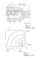
- FIG. 1 of the drawings A typical example of the electroluminescent panel is shown in FIG. 1 of the drawings.
- the prior art electroluminescent panel largely comprises a transparent package films 6 and light emitting body.
- the transparent package films 6 are laminated on each other, and are bonded to each other along the periphery 7 thereof (see FIG. 2 ).
- an inner space is defined between the transparent package films 6 , and the light emitting body is provided in the inner space.
- the light emitting body includes a non-transparent back electrode 1 , a transparent electrode 2 and a fluorescent layer 3 .
- the transparent electrode 2 is formed on the front surface of the fluorescent layer 3 , and the back surface of the fluorescent layer 3 is covered with the non-transparent back electrode 1 .
- the transparent electrode 2 is formed of indium tin oxide, and the back electrode 1 is formed of conventional conductive metal. When the transparent electrode 2 is biased with respect to the non-transparent back electrode 1 , the fluorescent layer 3 emits light as indicated by arrow in FIG. 2 .
- the electric power is supplied through a pair of power supply lines 4 to the transparent/back electrodes 2 / 1 .
- One of the power supply lines 4 is directly connected to the back electrode 1 .
- the other of the power supply lines 4 is connected to a non-transparent power feeding layer 5 , which is held in contact with the transparent electrode 2 .
- the non-transparent power feeding layer 5 is formed of silver paste.
- the non-transparent power feeding layer 5 is patterned like capital letter “I”, and extends along a side line of the transparent electrode 2 . The reason why the non-transparent power feeding layer 5 is required is that the silver paste is much smaller in resistivity than the indium tin oxide.
- the non-transparent power feeding layer 5 makes the transparent electrode 2 equal in potential level along the side line, and the gradation is moderated (see FIG. 4 ).
- the non-transparent power feeding layer 5 is desirable for the light emitting body in so far as the highly-resistive non-transparent electrode 2 is used for the light emitting body.
- the non-transparent power feeding layer 5 makes the light emitting surface narrow. In other words, dark area takes place in the prior art electroluminescent panel from the inner edge of the non-transparent power feeding layer 5 to the outer edge of the transparent package film 6 as indicated by hatching lines in FIG. 1 .
- the non-transparent power feeding layer 5 is patterned like capital letter “L”, i.e., extending along two end lines of the transparent electrode 2 , the gradation is further moderated. However, the dark area is widened. Thus, there is a trade-off between the gradation of brightness and the dark area.
- Research and development efforts have been made for an electroluminescent panel free from the problems.
- a solution is disclosed in Japanese Utility Model Publication of Unexamined Application No. 5-55494.
- the prior art electroluminescent panel disclosed therein has a light emitting body wrapped in package films.
- the light emitting body includes a fluorescent layer sandwiched between a transparent electrode and a back electrode.
- a difference from the light emitting body shown in FIG. 2 is an elongated transparent electrode.
- the transparent electrode of the light emitting body extends over the side line of the fluorescent layer, and is folded down under the back electrode.
- a power supply lead is held in contact with the back electrode, and the back electrode and the power supply lead are covered with a water absorbing layer.
- the folded portion of the transparent electrode is held in contact with the water absorbing layer.
- a non-transparent conductive metallic layer is patterned on the folded portion of the transparent electrode, and a power supply lead is connected to the non-transparent conductive metallic layer.
- the light emitting body When a bias voltage is applied between the transparent electrode and the back electrode, the light emitting body radiates light through the transparent electrode and the package film to the outside thereof. There is not any obstacle on the optical path from the light emitting body toward the outside. This results in that the dark area is narrowed.
- the present invention proposes to sideward radiate light from a folded portion of a light emitting body.
- an electroluminescent panel comprising a package having an inner space, a light emitting body accommodated in the inner space and including a fluorescent layer for emitting light, a high-conductive non-transparent electrode formed on one major surface of the fluorescent layer and a low-conductive transparent electrode formed on the other major surface of the fluorescent layer, at least a part of the fluorescent layer and an associated part of the low-conductive transparent electrode being folded so as to overlap the aforesaid one major surface therewith, and a power supply system including a first power supply lead connected to the high-conductive non-transparent electrode, a high-conductive power feeding layer formed on the associated part of the low-conductive transparent electrode and a second power supply lead connected to the high-conductive power feeding layer.
- a lighting device comprising plural electroluminescent panels for providing light emitting surface, and each of the electroluminescent panels comprising a package having an inner space, a light emitting body accommodated in the inner space and including a fluorescent layer for emitting light, a high-conductive non-transparent electrode formed on one major surface of the fluorescent layer and a low-conductive transparent electrode formed on the other major surface of the fluorescent layer, at least a part of the fluorescent layer and an associated part of the low-conductive transparent electrode being folded so as to overlap the aforesaid one major surface therewith and a power supply system including a first power supply lead connected to the high-conductive non-transparent electrode, a high-conductive power feeding layer formed on the associated part of the low-conductive transparent electrode and a second power supply lead connected to the high-conductive power feeding layer.
- FIG. 1 is a perspective view showing the prior art electroluminescent panel
- FIG. 2 is a cross sectional view taken along line B—B of FIG. 1 and showing the structure of the prior art electroluminescent panel;
- FIG. 3 is a plane view showing the brightness varied over the prior art electroluminescent panel
- FIG. 4 is a plane view showing another prior art electroluminescent panel
- FIG. 5 is a perspective view showing an electroluminescent panel according to the present invention.
- FIG. 6 is a cross sectional view taken along line A—A of FIG. 5 and showing the structure of the electroluminescent panel;
- FIG. 7 is a perspective view showing another electroluminescent panel according to the present invention.
- FIG. 8 is a perspective view showing yet another electroluminescent panel according to the present invention.
- FIG. 9 is a perspective view showing still another electroluminescent panel according to the present invention.
- FIG. 10 is a cross sectional view showing yet another electroluminescent panel according to the present invention.
- FIG. 11 is a cross sectional view showing still another electroluminescent panel according to the present invention.
- FIG. 12 is a plane view showing a lighting device according to the present invention.
- FIG. 13 is a cross sectional view taken along line C—C of FIG. 12 and showing the structure of the lighting device.
- an electroluminescent panel embodying the present invention largely comprises a pair of package films 6 , a light emitting body and a power supply system.
- One of the package films 6 is removed from the electroluminescent panel shown in FIG. 5 for clearly showing the light emitting body.
- the package films 6 are formed of synthetic resin, and are transparent.
- the package films 6 are bonded to one another along the periphery 7 thereof, and define an inner space (see figure 6 ).
- the package films 6 are moisture proof, and prevent the inner space from water and water vapor.
- the light emitting body includes a back electrode 1 , a transparent electrode 2 and a fluorescent layer 3 , and wider than the inner space.
- the light emitting body 1 / 2 / 3 is folded down, and has a flat portion and a folded portion.
- the folded portion emits light as well as the flat portion, and the light is radiated as indicated by arrows in FIG. 6 .
- the flat portion radiates the light in the normal direction
- the folded portion radiates the light toward the space over the periphery 7 , and makes the peripheral area 7 bright.
- the fluorescent layer 3 is formed like a sheet, and contains fluorescent substance.
- the back electrode 1 is, by way of example, formed of aluminum.
- the back electrode 1 is as wide as the fluorescent layer 3 , and the back surface of the fluorescent layer 3 is covered with the back electrode 1 .
- the transparent electrode 2 is formed of transparent conductive material such as, for example, indium tin oxide.
- the transparent electrode 2 is also as wide as the fluorescent layer 3 , and the front surface of the fluorescent layer 3 is covered with the transparent electrode 2 .
- the power supply system biases the light emitting body with alternating current voltage.
- the power supply system includes a pair of power supply lines 4 and a non-transparent power feeding layer 5 .
- Silver paste is printed on the transparent electrode 2 , and is fired so as to form the non-transparent power feeding layer 5 .
- the non-transparent power feeding layer 5 is formed on the transparent electrode 2 of the folded portion, and is patterned like capital letter “I” (see FIG. 5 ). In other words, the non-transparent power feeding layer 5 has a stripe shape, and extends along a side line of the light emitting body.
- the non-transparent power feeding layer 5 makes the potential level uniform along the side line of the folded portion.
- One of the power supply lines 4 is directly connected to the back electrode 1 .
- the other of the power supply lines 4 is held in contact with the non-transparent power feeding layer 5 , and is electrically connected through the non-transparent power feeding layer 5 to the transparent electrode 2 . Only the power supply lines 4 project into the inner space, and package films 6 are partially separated for passing the power supply lines 4 . However, the package films 6 hermetically seals the light emitting body inside thereof.
- the alternating current voltage is propagated from the side portion of the folded portion beneath the non-transparent power feeding layer 5 toward the other side line of the transparent electrode 2 , and the potential drop is smaller than that in the light emitting body of the prior art electroluminescent panel shown in FIG. 3, because the distance between the side lines is shorter than the distance between two corners.
- Light is radiated from the electroluminescent panel according to the present invention as follows. Alternating current voltage is supplied between the transparent electrode 2 and the back electrode 1 . The alternating current voltage ranges from 50 volts to 100 volts, and the frequency is fallen within the range between 50 Hz and 1000 Hz. The alternating current voltage creates an alternating electric field across the fluorescent layer 3 , and causes the fluorescent layer 3 to emit the light. The light is radiated from the fluorescent layer 3 through the entire surface of the transparent electrode 2 . Although any light emitting mean is not inserted between the package films 6 in the peripheral area 7 , the light is radiated from the folded portion through the transparent package film 6 toward the space over the peripheral area 7 as indicated by the right arrow in FIG. 6, and makes the space over the peripheral area 7 bright as if the light emitting body is sandwiched between the package films 6 in the peripheral area 7 .
- the back electrode 1 and the transparent electrode 2 are formed on both surfaces of the fluorescent layer 3 , and, thereafter, the non-transparent power feeding layer 5 is patterned on the transparent electrode 2 along the side line. Subsequently, the lamination 1 / 2 / 3 is folded along the side line, and the power supply leads 4 are connected to the back electrode 1 and the non-transparent power feeding layer 5 . Finally, light emitting body 1 / 2 / 3 / is sealed in the inner space between the package films 6 .
- the non-transparent power feeding layer 5 may be patterned on the transparent electrode 2 of the folded portion after the folding work.
- the non-transparent power feeding layer 5 is exactly located on the transparent electrode 2 of the folded portion.
- the light emitting body per se is folded down, and the light is emitted from the folded portion as well as the flat portion, and the light from the folded portion makes the space over the peripheral area bright.
- the non-transparent power feeding layer 5 and the back electrode 1 are provided on the same side with respect to the fluorescent layer 3 of the flat portion, and there is not any obstacle against the radiated light on the transparent electrode 2 of the flat portion. This results in that the dark area is substantially eliminated from the electroluminescent panel according to the present invention.
- another electroluminescent panel embodying the present invention also largely comprises a pair of package films 6 , a light emitting body 21 and a power supply system 4 / 51 .
- the light emitting body 21 is scaled in an inner space between the package films, the upper package film 6 is removed from the electroluminescent panel shown in FIG. 7 .
- the removal of the upper package film 6 makes the light emitting body 21 clear.
- the light emitting body 21 is a lamination of a back electrode, a fluorescent layer and a transparent electrode as similar to the first embodiment.
- a difference between the light emitting bodies 21 and 1 / 2 / 3 is the folded portion.
- the light emitting body 1 / 2 / 3 is folded down along one of the side lines.
- the light emitting body 21 is folded down along one side line and one end line, and has a flat portion and an L-shaped folded portion.
- the non-transparent power feeding layer 51 is patterned like capital letter “L”, and extends on the folded portion along the side line and the end line.
- the folded portion of the light emitting body 51 radiates the light toward the space over the L-shaped peripheral area, and makes the space over the L-shaped peripheral area bright.
- the electroluminescent panel implementing the second embodiment reduces the dark area.
- the L-shaped power feeding layer 51 further reduces the potential drop on the transparent electrode, and the gradation of brightness is further improved.
- the electroluminescent panel implementing the second embodiment is fabricated as similar to the first embodiment.
- FIG. 8 illustrates yet another electroluminescent panel embodying the present invention
- the electroluminescent panel implementing the third embodiment also largely comprises a pair of package films 6 , a light emitting body 22 and a power supply system 4 / 61 .
- the light emitting body 22 is scaled in an inner space between the package films, the upper package film 6 is removed from the electroluminescent panel shown in FIG. 8 .
- the removal of the upper package film 6 makes the light emitting body 22 clear.
- the light emitting body 22 is a lamination of a back electrode, a fluorescent layer and a transparent electrode as similar to the first embodiment.
- a difference between the light emitting bodies 22 and 1 / 2 / 3 is the folded portion.
- the light emitting body 1 / 2 / 3 is only folded down along one of the side lines.
- the light emitting body 22 is folded down along two side line and one end line, and has a flat portion and a U-shaped folded portion.
- the non-transparent power feeding layer 61 is patterned like capital letter “U”, and extends on the folded portion along the two side lines and the end line.
- the folded portion of the light emitting body 61 radiates the light toward the space over the U-shaped peripheral area, and makes the space over the U-shaped peripheral area bright.
- the electroluminescent panel implementing the second embodiment reduces the dark area.
- the U-shaped power feeding layer 61 reduces the potential drop on the transparent electrode and, accordingly, the gradation of brightness.
- the electroluminescent panel implementing the third embodiment is fabricated as similar to the first embodiment.
- FIG. 9 illustrates still another electroluminescent panel embodying the present invention, and the electroluminescent panel implementing the fourth embodiment also largely comprises a pair of package films 6 , a light emitting body 23 and a power supply system 4 / 71 .
- the light emitting body 23 is sealed in an inner space between the package films, the upper package film 6 is removed from the electroluminescent panel shown in FIG. 9 .
- the removal of the upper package film 6 makes the light emitting body 23 clear.
- the light emitting body 23 is a lamination of a back electrode, a fluorescent layer and a transparent electrode as similar to the first embodiment.
- a difference between the light emitting bodies 23 and 1 / 2 / 3 is the folded portion.
- the light emitting body 1 / 2 / 3 is only folded down along one of the side lines.
- the light emitting body 23 is folded down along the entire periphery, i.e., two side lines and two end lines, and has a fiat portion and a looped folded portion.
- the non-transparent power feeding layer 71 is looped, and extends on the folded portion along the periphery.
- the folded portion of the light emitting body 71 radiates the light toward the space over the looped peripheral area, and makes the space over the looped peripheral area bright.
- the electroluminescent panel implementing the second embodiment perfectly reduces the dark area.
- the U-shaped power feeding layer 71 reduces the potential drop on the transparent electrode and, accordingly, the gradation of brightness.
- the electroluminescent panel implementing the fourth embodiment is fabricated as similar to the first embodiment.
- FIG. 10 illustrates yet another electroluminescent panel embodying the present invention.
- the electroluminescent panel implementing the fifth embodiment also largely comprises a pair of package films 6 , a light emitting body 81 and a power supply system 4 / 5 .
- the light emitting body 81 is sealed in an inner space between the package films 6 .
- the light emitting body 81 includes a back electrode 14 , a fluorescent layer 3 and a transparent electrode 2 .
- the light emitting body is folded down along one side line, and the non transparent power feeding layer 5 is patterned like capital letter “I” on the transparent electrode of the folded portion along the side line.
- the electroluminescent panel implementing the fifth embodiment achieves all the advantages of the first embodiment.
- a difference between the light emitting body 1 / 2 / 3 and 81 is the back electrode 14 .
- the back electrode 1 is as wide as the transparent electrode 2 and the fluorescent layer 3 , and is folded down.
- the back electrode 1 of the folded portion is laminated on that of the flat portion. This results in increase in thickness of the electroluminescent panel.
- the back electrode 14 is narrower than the transparent electrode 2 and the fluorescent layer 3 . In other words, the back electrode 14 is removed from the folded portion of the light emitting body 81 , and the fluorescent layer 3 of the folded portion is directly held in contact with the back electrode 14 of the flat portion. This results in decrease in thickness of the electroluminescent panel.
- the electroluminescent panel implementing the fifth embodiment is fabricated as similar to the first embodiment.
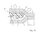
- FIG. 11 illustrates still another electroluminescent panel embodying the present invention.
- the electroluminescent panel embodying the present invention largely comprises a pair of package films 6 , a light emitting body 91 and a power supply system 4 / 5 .
- the light emitting body 91 is sealed in an inner space between the package films 6 , and is biased through the power supply system 4 / 5 .
- the light emitting body 91 radiates light toward the space over the peripheral area 7 , and the light makes the space over the peripheral area 7 bright.
- the light emitting body 91 includes the back electrode 14 , the transparent electrode 2 and a fluorescent layer 34 .
- the back electrode 14 is narrower than the transparent electrode 2 and the fluorescent layer 34 as similar to that of the fifth embodiment.
- the fluorescent layer 34 is partially reduced in thickness. Namely, the fluorescent layer 34 of the flat portion is relatively thick, and the fluorescent layer 34 of the folded portion is relatively thin. When the light emitting body 91 is folded down, the relatively thin fluorescent layer 34 is held in contact with the back electrode 14 . The total thickness is further reduced.
- the fluorescent layer 34 is desirable for the electroluminescent panels implementing the second, third and fourth embodiments. If the fluorescent layer is constant in thickness, the light emitting body 21 / 23 / 24 is increased in thickness at the corner or corners thereof, because the light emitting body 21 / 23 / 24 is folded twice at the corner or corners. Even if the fluorescent layer is laminated twice or thrice, the fluorescent layer 34 of the folded portion prevents the corner or corners from increase of thickness.
- the electroluminescent panel implementing the sixth embodiment is fabricated as similar to the first embodiment.
- the electroluminescent panel according to the present invention reduces the dark with the light radiated from the folded portion. Moreover, the non-transparent power feeding layer is patterned on the transparent electrode of the folded portion along one or more than one side line, and the uniformity of brightness is improved.
- the electroluminescent panels are arranged in matrix for forming a lighting device appropriate for a panel display as shown in FIGS. 12 and 13. Any one of the electroluminescent panels shown in FIGS. 5 to 11 is available for the lighting device. In this instance, the electroluminescent panel implementing the second embodiment is used for the lighting device.
- Plural electroluminescent panels are arranged in matrix for forming the light device.
- the upper package films 6 are removed from the electroluminescent panels so as to clearly show the light emitting bodies 21 .
- the array of plural electroluminescent panels measures 250 millimeters by 250 millimeters. However, it is possible to form a lighting device wider than that shown in FIG. 12 .
- Each of the electroluminescent panels has the L-shaped non-transparent power feeding layer 51 on the folded portion of the light emitting body 21 .
- the electroluminescent panels are arranged in such a manner that each of the L-shaped non-transparent power feeding layers 51 is opposed to those of the adjacent L-shaped non-transparent power feeding layers 51 .
- the location of the L-shaped non-transparent power feeding layers 51 are indicated by hatching lines in FIG. 12, and the L-shaped non-transparent power feeding layers 51 form a large cross. Accordingly, the folded portions of the light emitting bodies 51 are located like the large cross.
- the light emitting bodies 21 When the light emitting bodies 21 are biased with the alternating current voltage, light is emitted from the folded portions of the light emitting bodies 21 as well as the flat portions thereof (see FIG. 13 ).
- the folded portions illuminate the space over the peripheral areas, and the lighting device makes the entire surface thereof bright without any dark area.
- the lighting device is appropriate for a display panel such as, for example, a liquid crystal display panel.
- the electroluminescent panel according to the present invention is available for a wide lighting device uniform in brightness.
- an electroluminescent panel according to the present invention may be biased with direct current voltage.
- the transparent electrode 2 may be patterned into a certain image.
- a light emitting body is partially cut away at the corner or corners before being folded. In this instance, there is not any corner folded twice. For this reason, the electroluminescent panel is constant in thickness along the periphery thereof.
Abstract
Description
Claims (5)
Applications Claiming Priority (2)
| Application Number | Priority Date | Filing Date | Title |
|---|---|---|---|
| JP23319799A JP3538080B2 (en) | 1999-08-19 | 1999-08-19 | Electroluminescent lighting device |
| JP11-233197 | 1999-08-19 |
Publications (1)
| Publication Number | Publication Date |
|---|---|
| US6630783B1 true US6630783B1 (en) | 2003-10-07 |
Family
ID=16951280
Family Applications (1)
| Application Number | Title | Priority Date | Filing Date |
|---|---|---|---|
| US09/639,460 Expired - Fee Related US6630783B1 (en) | 1999-08-19 | 2000-08-16 | Electroluminescent panel with folded light emitting body |
Country Status (4)
| Country | Link |
|---|---|
| US (1) | US6630783B1 (en) |
| JP (1) | JP3538080B2 (en) |
| KR (1) | KR100434622B1 (en) |
| TW (1) | TW471236B (en) |
Cited By (4)
| Publication number | Priority date | Publication date | Assignee | Title |
|---|---|---|---|---|
| US20090179322A1 (en) * | 2007-12-12 | 2009-07-16 | International Business Machines Corporation | Electronic package method and structure with cure-melt hierarchy |
| US20110216520A1 (en) * | 2010-03-02 | 2011-09-08 | Erik Sowder | Photographic system |
| EP2133854A4 (en) * | 2007-03-30 | 2011-11-30 | Pioneer Corp | Light emitting device |
| US9111470B2 (en) | 2011-07-13 | 2015-08-18 | Lori Anderson | Retractable electroluminescent display system |
Families Citing this family (1)
| Publication number | Priority date | Publication date | Assignee | Title |
|---|---|---|---|---|
| CN103299714B (en) * | 2010-12-28 | 2016-01-20 | 夏普株式会社 | The manufacture method of organic EL display unit, organic EL display and organic EL display unit |
Citations (12)
| Publication number | Priority date | Publication date | Assignee | Title |
|---|---|---|---|---|
| US3252035A (en) * | 1963-02-25 | 1966-05-17 | Westinghouse Electric Corp | Electroluminescent lamp with built-in rearwardly-disposed input terminals |
| US3384770A (en) * | 1966-07-18 | 1968-05-21 | Gen Electric | Electroluminescent display device having folded elements |
| US3497750A (en) * | 1966-12-02 | 1970-02-24 | Westinghouse Electric Corp | Flexible electroluminescent lamp with dual-purpose metallized plastic film component |
| US3509401A (en) * | 1967-08-24 | 1970-04-28 | Sylvania Electric Prod | Encapsulated electroluminescent device |
| US4730146A (en) * | 1986-10-21 | 1988-03-08 | W. H. Brady Co. | Folded electroluminescent lamp assembly |
| US4914348A (en) * | 1987-12-03 | 1990-04-03 | Ricoh Company, Ltd. | Electroluminescence multi-color display device |
| US5120618A (en) * | 1989-03-09 | 1992-06-09 | Stanley Electric Co., Ltd. | Electroluminescent panel |
| JPH0555494A (en) | 1991-08-22 | 1993-03-05 | Yokogawa Electric Corp | High-voltage mos ic |
| US5302468A (en) * | 1992-01-28 | 1994-04-12 | Pioneer Electronic Corporation | Organic electroluminescent display apparatus |
| US5786664A (en) * | 1995-03-27 | 1998-07-28 | Youmin Liu | Double-sided electroluminescent device |
| US6091192A (en) * | 1998-02-02 | 2000-07-18 | Winsor Corporation | Stress-relieved electroluminescent panel |
| US6124672A (en) * | 1995-03-30 | 2000-09-26 | Dynamic Brilliance Corporation | Electroluminescent device with a secure contact |
-
1999
- 1999-08-19 JP JP23319799A patent/JP3538080B2/en not_active Expired - Fee Related
-
2000
- 2000-08-15 TW TW089116425A patent/TW471236B/en not_active IP Right Cessation
- 2000-08-16 US US09/639,460 patent/US6630783B1/en not_active Expired - Fee Related
- 2000-08-18 KR KR10-2000-0047815A patent/KR100434622B1/en not_active IP Right Cessation
Patent Citations (12)
| Publication number | Priority date | Publication date | Assignee | Title |
|---|---|---|---|---|
| US3252035A (en) * | 1963-02-25 | 1966-05-17 | Westinghouse Electric Corp | Electroluminescent lamp with built-in rearwardly-disposed input terminals |
| US3384770A (en) * | 1966-07-18 | 1968-05-21 | Gen Electric | Electroluminescent display device having folded elements |
| US3497750A (en) * | 1966-12-02 | 1970-02-24 | Westinghouse Electric Corp | Flexible electroluminescent lamp with dual-purpose metallized plastic film component |
| US3509401A (en) * | 1967-08-24 | 1970-04-28 | Sylvania Electric Prod | Encapsulated electroluminescent device |
| US4730146A (en) * | 1986-10-21 | 1988-03-08 | W. H. Brady Co. | Folded electroluminescent lamp assembly |
| US4914348A (en) * | 1987-12-03 | 1990-04-03 | Ricoh Company, Ltd. | Electroluminescence multi-color display device |
| US5120618A (en) * | 1989-03-09 | 1992-06-09 | Stanley Electric Co., Ltd. | Electroluminescent panel |
| JPH0555494A (en) | 1991-08-22 | 1993-03-05 | Yokogawa Electric Corp | High-voltage mos ic |
| US5302468A (en) * | 1992-01-28 | 1994-04-12 | Pioneer Electronic Corporation | Organic electroluminescent display apparatus |
| US5786664A (en) * | 1995-03-27 | 1998-07-28 | Youmin Liu | Double-sided electroluminescent device |
| US6124672A (en) * | 1995-03-30 | 2000-09-26 | Dynamic Brilliance Corporation | Electroluminescent device with a secure contact |
| US6091192A (en) * | 1998-02-02 | 2000-07-18 | Winsor Corporation | Stress-relieved electroluminescent panel |
Cited By (10)
| Publication number | Priority date | Publication date | Assignee | Title |
|---|---|---|---|---|
| EP2133854A4 (en) * | 2007-03-30 | 2011-11-30 | Pioneer Corp | Light emitting device |
| US20090179322A1 (en) * | 2007-12-12 | 2009-07-16 | International Business Machines Corporation | Electronic package method and structure with cure-melt hierarchy |
| US7834442B2 (en) | 2007-12-12 | 2010-11-16 | International Business Machines Corporation | Electronic package method and structure with cure-melt hierarchy |
| US20110216520A1 (en) * | 2010-03-02 | 2011-09-08 | Erik Sowder | Photographic system |
| US20110217028A1 (en) * | 2010-03-02 | 2011-09-08 | Erik Sowder | Formable photographic device |
| US20110216519A1 (en) * | 2010-03-02 | 2011-09-08 | Erik Sowder | Photographic devices |
| US8457483B2 (en) | 2010-03-02 | 2013-06-04 | Expolmaging, Inc. | Photographic system |
| US8591049B2 (en) | 2010-03-02 | 2013-11-26 | ExpoImaging, Inc. | Photographic devices |
| US8774612B2 (en) | 2010-03-02 | 2014-07-08 | ExpoImaging, Inc. | Formable photographic device |
| US9111470B2 (en) | 2011-07-13 | 2015-08-18 | Lori Anderson | Retractable electroluminescent display system |
Also Published As
| Publication number | Publication date |
|---|---|
| KR100434622B1 (en) | 2004-06-05 |
| KR20010021354A (en) | 2001-03-15 |
| TW471236B (en) | 2002-01-01 |
| JP2001057288A (en) | 2001-02-27 |
| JP3538080B2 (en) | 2004-06-14 |
Similar Documents
| Publication | Publication Date | Title |
|---|---|---|
| US20030227767A1 (en) | Backlight assembly and liquid crystal display apparatus | |
| US8536568B2 (en) | Display device | |
| EP1662301A1 (en) | Lighting device and reflective liquid crystal display with the lighting device | |
| JPH05205875A (en) | Organic electroluminescent display unit | |
| KR100623845B1 (en) | Backlight assembly and liquid crystal display device having thereof | |
| JP4711273B2 (en) | Illuminated liquid crystal display device | |
| US6043605A (en) | Plasma display device with auxiliary electrodes and protective layer | |
| JP2000207917A (en) | Backlight assembly for liquid crystal display device module | |
| JP2831730B2 (en) | Contact image sensor | |
| US6630783B1 (en) | Electroluminescent panel with folded light emitting body | |
| KR20180001464A (en) | Light emitting device | |
| US6107735A (en) | Electroluminescent lamp | |
| CN110908192B (en) | Backlight module and display device | |
| US20050083712A1 (en) | Backlight unit | |
| KR101631617B1 (en) | Liquid crystal display device | |
| US7378786B2 (en) | Surface light source device and liquid crystal display apparatus having the same | |
| JP3821239B2 (en) | Liquid crystal display | |
| JPH074793Y2 (en) | EL element structure | |
| JP5704290B1 (en) | Light emitting device | |
| JP3065082U (en) | Mirror device with luminescence display function | |
| JP3247910B2 (en) | Display device | |
| JPH088066A (en) | Electroluminescent lamp | |
| KR0147547B1 (en) | Electroluminescence element | |
| JP2000003792A (en) | Electroluminescent lamp | |
| KR20070079175A (en) | Flat fluorescent lamp and liquid crystal display having the same |
Legal Events
| Date | Code | Title | Description |
|---|---|---|---|
| AS | Assignment |
Owner name: NEC CORPORATION, JAPAN Free format text: ASSIGNMENT OF ASSIGNORS INTEREST;ASSIGNOR:ONO, SHINICHIROU;REEL/FRAME:011013/0298 Effective date: 20000807 |
|
| AS | Assignment |
Owner name: NEC LCD TECHNOLOGIES, LTD., JAPAN Free format text: ASSIGNMENT OF ASSIGNORS INTEREST;ASSIGNOR:NEC CORPORATION;REEL/FRAME:013577/0142 Effective date: 20030401 |
|
| FEPP | Fee payment procedure |
Free format text: PAYOR NUMBER ASSIGNED (ORIGINAL EVENT CODE: ASPN); ENTITY STATUS OF PATENT OWNER: LARGE ENTITY |
|
| FPAY | Fee payment |
Year of fee payment: 4 |
|
| AS | Assignment |
Owner name: NEC CORPORATION,JAPAN Free format text: ASSIGNMENT OF ASSIGNORS INTEREST;ASSIGNOR:NEC LCD TECHNOLOGIES, LTD.;REEL/FRAME:024492/0176 Effective date: 20100301 Owner name: NEC CORPORATION, JAPAN Free format text: ASSIGNMENT OF ASSIGNORS INTEREST;ASSIGNOR:NEC LCD TECHNOLOGIES, LTD.;REEL/FRAME:024492/0176 Effective date: 20100301 |
|
| FEPP | Fee payment procedure |
Free format text: PAYER NUMBER DE-ASSIGNED (ORIGINAL EVENT CODE: RMPN); ENTITY STATUS OF PATENT OWNER: LARGE ENTITY Free format text: PAYOR NUMBER ASSIGNED (ORIGINAL EVENT CODE: ASPN); ENTITY STATUS OF PATENT OWNER: LARGE ENTITY |
|
| FPAY | Fee payment |
Year of fee payment: 8 |
|
| AS | Assignment |
Owner name: GETNER FOUNDATION LLC, DELAWARE Free format text: ASSIGNMENT OF ASSIGNORS INTEREST;ASSIGNOR:NEC CORPORATION;REEL/FRAME:026254/0381 Effective date: 20110418 |
|
| REMI | Maintenance fee reminder mailed | ||
| LAPS | Lapse for failure to pay maintenance fees | ||
| STCH | Information on status: patent discontinuation |
Free format text: PATENT EXPIRED DUE TO NONPAYMENT OF MAINTENANCE FEES UNDER 37 CFR 1.362 |
|
| FP | Lapsed due to failure to pay maintenance fee |
Effective date: 20151007 |
|
| AS | Assignment |
Owner name: VISTA PEAK VENTURES, LLC, TEXAS Free format text: ASSIGNMENT OF ASSIGNORS INTEREST;ASSIGNOR:GETNER FOUNDATION LLC;REEL/FRAME:045469/0164 Effective date: 20180213 |