US6633365B2 - Projection optical system and exposure apparatus having the projection optical system - Google Patents
Projection optical system and exposure apparatus having the projection optical system Download PDFInfo
- Publication number
- US6633365B2 US6633365B2 US10/006,667 US666701A US6633365B2 US 6633365 B2 US6633365 B2 US 6633365B2 US 666701 A US666701 A US 666701A US 6633365 B2 US6633365 B2 US 6633365B2
- Authority
- US
- United States
- Prior art keywords
- lens
- lens group
- optical system
- projection optical
- mask
- Prior art date
- Legal status (The legal status is an assumption and is not a legal conclusion. Google has not performed a legal analysis and makes no representation as to the accuracy of the status listed.)
- Expired - Lifetime
Links
- 230000003287 optical effect Effects 0.000 title claims abstract description 159
- 238000000034 method Methods 0.000 claims description 49
- 239000000758 substrate Substances 0.000 claims description 28
- 238000004519 manufacturing process Methods 0.000 claims description 15
- 238000005286 illumination Methods 0.000 claims description 9
- 239000007788 liquid Substances 0.000 claims description 8
- 230000015572 biosynthetic process Effects 0.000 claims description 7
- 230000002265 prevention Effects 0.000 claims description 5
- 230000005499 meniscus Effects 0.000 description 51
- 230000004075 alteration Effects 0.000 description 34
- 239000004973 liquid crystal related substance Substances 0.000 description 14
- 239000000463 material Substances 0.000 description 10
- 239000004065 semiconductor Substances 0.000 description 9
- 206010073261 Ovarian theca cell tumour Diseases 0.000 description 8
- 208000001644 thecoma Diseases 0.000 description 8
- 238000000206 photolithography Methods 0.000 description 4
- 206010010071 Coma Diseases 0.000 description 3
- 210000004027 cell Anatomy 0.000 description 3
- 210000002858 crystal cell Anatomy 0.000 description 3
- 230000006866 deterioration Effects 0.000 description 3
- 239000011521 glass Substances 0.000 description 3
- 230000007261 regionalization Effects 0.000 description 3
- 230000000452 restraining effect Effects 0.000 description 3
- XLYOFNOQVPJJNP-UHFFFAOYSA-N water Substances O XLYOFNOQVPJJNP-UHFFFAOYSA-N 0.000 description 3
- VYPSYNLAJGMNEJ-UHFFFAOYSA-N Silicium dioxide Chemical compound O=[Si]=O VYPSYNLAJGMNEJ-UHFFFAOYSA-N 0.000 description 2
- 230000018109 developmental process Effects 0.000 description 2
- 238000005530 etching Methods 0.000 description 2
- 238000007654 immersion Methods 0.000 description 2
- 229920002120 photoresistant polymer Polymers 0.000 description 2
- 230000004304 visual acuity Effects 0.000 description 2
- 238000005452 bending Methods 0.000 description 1
- 238000010276 construction Methods 0.000 description 1
- 230000000694 effects Effects 0.000 description 1
- 238000010348 incorporation Methods 0.000 description 1
- 230000010354 integration Effects 0.000 description 1
- 239000011159 matrix material Substances 0.000 description 1
- 238000010943 off-gassing Methods 0.000 description 1
- 239000010453 quartz Substances 0.000 description 1
- 238000004904 shortening Methods 0.000 description 1
- 239000000126 substance Substances 0.000 description 1
- 239000008400 supply water Substances 0.000 description 1
- 239000010409 thin film Substances 0.000 description 1
- 238000007740 vapor deposition Methods 0.000 description 1
Images


Classifications
-
- G—PHYSICS
- G03—PHOTOGRAPHY; CINEMATOGRAPHY; ANALOGOUS TECHNIQUES USING WAVES OTHER THAN OPTICAL WAVES; ELECTROGRAPHY; HOLOGRAPHY
- G03F—PHOTOMECHANICAL PRODUCTION OF TEXTURED OR PATTERNED SURFACES, e.g. FOR PRINTING, FOR PROCESSING OF SEMICONDUCTOR DEVICES; MATERIALS THEREFOR; ORIGINALS THEREFOR; APPARATUS SPECIALLY ADAPTED THEREFOR
- G03F7/00—Photomechanical, e.g. photolithographic, production of textured or patterned surfaces, e.g. printing surfaces; Materials therefor, e.g. comprising photoresists; Apparatus specially adapted therefor
- G03F7/70—Microphotolithographic exposure; Apparatus therefor
- G03F7/70216—Mask projection systems
- G03F7/70241—Optical aspects of refractive lens systems, i.e. comprising only refractive elements
-
- G—PHYSICS
- G02—OPTICS
- G02B—OPTICAL ELEMENTS, SYSTEMS OR APPARATUS
- G02B13/00—Optical objectives specially designed for the purposes specified below
- G02B13/14—Optical objectives specially designed for the purposes specified below for use with infrared or ultraviolet radiation
- G02B13/143—Optical objectives specially designed for the purposes specified below for use with infrared or ultraviolet radiation for use with ultraviolet radiation
-
- G—PHYSICS
- G02—OPTICS
- G02B—OPTICAL ELEMENTS, SYSTEMS OR APPARATUS
- G02B27/00—Optical systems or apparatus not provided for by any of the groups G02B1/00 - G02B26/00, G02B30/00
- G02B27/18—Optical systems or apparatus not provided for by any of the groups G02B1/00 - G02B26/00, G02B30/00 for optical projection, e.g. combination of mirror and condenser and objective
-
- G—PHYSICS
- G03—PHOTOGRAPHY; CINEMATOGRAPHY; ANALOGOUS TECHNIQUES USING WAVES OTHER THAN OPTICAL WAVES; ELECTROGRAPHY; HOLOGRAPHY
- G03F—PHOTOMECHANICAL PRODUCTION OF TEXTURED OR PATTERNED SURFACES, e.g. FOR PRINTING, FOR PROCESSING OF SEMICONDUCTOR DEVICES; MATERIALS THEREFOR; ORIGINALS THEREFOR; APPARATUS SPECIALLY ADAPTED THEREFOR
- G03F7/00—Photomechanical, e.g. photolithographic, production of textured or patterned surfaces, e.g. printing surfaces; Materials therefor, e.g. comprising photoresists; Apparatus specially adapted therefor
- G03F7/70—Microphotolithographic exposure; Apparatus therefor
- G03F7/70216—Mask projection systems
- G03F7/70341—Details of immersion lithography aspects, e.g. exposure media or control of immersion liquid supply
Definitions
- the present invention relates to a projection optical system and to an exposure apparatus to which such a projection optical system is fitted, and more particularly relates to a projection optical system which is suitable for an exposure apparatus which is used for the manufacture of semiconductor elements or liquid crystal display elements and the like by a process of photolithography.
- the resolving power which is required from the projection optical system is increasing along with increase of the degree of integration of the semiconductor elements or the like. Due to this, along with shortening the wavelength of the illumination light (the exposure light), a compelling necessity is experienced for raising the image side numerical aperture (NA) of the projection optical system to the ultimate limit, in order to satisfy this requirement for resolving power of the projection optical system.
- NA numerical aperture
- the lens outer diameter is increased in proportion to the size of the numerical aperture.
- the outer diameter (the glass material diameter) of the block of optical material from which this lens is manufactured also becomes great, and it becomes difficult to obtain an optical material block of the required homogeneity, and therefore it is hard to manufacture an optical system of good performance.
- the lens outer diameter becomes great, the lens can easily be influenced by bending or distortion due to its weight, which also makes it difficult to manufacture an optical system of good performance.
- the objective of the present invention is to provide a high resolution projection optical system, and an exposure apparatus to which such a projection optical system is fitted, which are capable of ensuring a large image side numerical aperture, while restraining increase in the size of the lens outer diameter. Furthermore, it is another objective of the present invention to provide a method of microdevice manufacture, which can manufacture a good quality microdevice at high accuracy by utilizing an exposure apparatus according to the present invention as defined above, to which is fitted a high resolution projection optical system which has a large image side numerical aperture.
- a projection optical system whose image side numerical aperture is greater than or equal to 0.75, and which forms an image of a first object upon a second object using light of a predetermined wavelength less than or equal to 300 nm, comprises: a first lens group G 1 of positive refractive power; a second lens group G 2 of negative refractive power; a third lens group G 3 of positive refractive power; and a fourth lens group G 4 of positive refractive power, and: the first lens group G 1 , the second lens group G 2 , the third lens group G 3 and the fourth lens group G 4 are arranged in order from a side of the first object; and a distance D in mm along an optical axis between an optical surface of the fourth lens group G 4 closest to the second object, and the second object, satisfies a condition of 0.1 ⁇ D ⁇ 5.
- the projection optical system has an image side numerical aperture greater than or equal to 0.8.
- T being a sum of thicknesses along the optical axis of all optical members included in the fourth lens group G 4
- D being the distance along the optical axis between the optical surface of the fourth lens group G 4 closest to the second object, and the second object
- T being a sum of the thicknesses along the optical axis of all optical members included in the fourth lens group G 4
- L being a distance along the optical axis between the first object and the second object
- a distance L in mm along the optical axis between the first object and the second object satisfies a condition of 800 ⁇ L ⁇ 1600.
- a focal length F 2 of the second lens group G 2 and a distance L in mm along the optical axis between the first object and the second object satisfy a condition of 0.01 ⁇
- At least one of a plurality of optical surfaces comprised in the projection optical system is formed in an aspherical shape.
- An exposure apparatus comprises: an illumination system for illuminating a mask as a first object; a projection optical system described above that forms an image of a pattern which is formed upon the mask upon a photosensitive substrate as the second object; and a prevention device that prevents gas which is generated from the photosensitive substrate from adhering to the optical surface closest to the second object of the fourth lens group G 4 of the projection optical system.
- the prevention device comprises a flow forming device that forms a predetermined flow of gas or liquid in a optical path between the optical surface closest to the second object of the fourth lens group G 4 and the photosensitive substrate.
- An exposure method comprises: an illumination process of illuminating a mask as a first object; and an exposure process of exposing, via a projection optical system described above, an image of a pattern which is formed upon the mask upon a photosensitive substrate as the second object, and the exposure process comprises a flow formation process of forming a predetermined flow of gas or liquid in a optical path between the optical surface closest to the second object of the fourth lens group G 4 and the photosensitive substrate, in order to prevent gas which is generated from the photosensitive substrate from adhering to the optical surface closest to the second object of the fourth lens group G 4 .
- a method according to the present invention for manufacturing a microdevice comprises: an exposure process of exposing a pattern on a mask upon a photosensitive substrate, using an exposure method described above; and a development process of developing the photosensitive substrate which has been exposed by the exposure process.
- FIG. 1 is a figure schematically showing the structure of an exposure apparatus equipped with a projection optical system which is a preferred embodiment of the present invention.
- FIG. 2 is a figure showing the structure of lenses of a projection optical system according to a first preferred embodiment of the present invention.
- FIG. 3 is a figure showing the coma aberration of this projection optical system according to the first preferred embodiment of the present invention.
- FIG. 4 is a figure showing the structure of lenses of a projection optical system according to a second preferred embodiment of the present invention.
- FIG. 5 is a figure showing the coma aberration of this projection optical system according to the second preferred embodiment of the present invention.
- FIG. 6 is a figure showing the structure of lenses of a projection optical system according to a third preferred embodiment of the present invention.
- FIG. 7 is a figure showing the coma aberration of this projection optical system according to the third preferred embodiment of the present invention.
- FIG. 8 is a flow chart showing a procedure when manufacturing a semiconductor device which is a microdevice.
- FIG. 9 is a flow chart showing a procedure when manufacturing a liquid crystal display element which is a microdevice.
- the lens outer diameter also becomes greater in proportion to the increase of the image side numerical aperture.
- the lens surface of a projection optical system which is closest to the image side is formed in a shape which has small curvature and is close to a plane.
- the amount of high order spherical aberration which is generated is nearly proportional to the above described working distance D.
- the working distance D is set to be small, it is possible to suppress the generation of high order spherical aberration to a low level, and it is possible to restrain the lens outer diameter to be comparatively small, even if the image side numerical aperture is made large.
- the working distance D is set within a relatively small predetermined range according to the following condition (1), with a basic construction which comprises, in order from the object side (the mask side): a first lens group G 1 of positive refractive power; a second lens group G 2 of negative refractive power; a third lens group of positive refractive power; and a fourth lens group G 4 also of positive refractive power.
- a basic construction which comprises, in order from the object side (the mask side): a first lens group G 1 of positive refractive power; a second lens group G 2 of negative refractive power; a third lens group of positive refractive power; and a fourth lens group G 4 also of positive refractive power.
- the working distance D (units mm) along the optical axis between the optical surface of the fourth lens group G 4 which is closest to the second object (which is closest to the image side: which in the case of an exposure apparatus is the extreme optical surface in the direction of the wafer) and the second object (which in the case of an exposure apparatus is the wafer) should satisfy the following condition (1):
- the working distance D exceeds the upper limit value of the above condition (1), the working distance D becomes too large, and the incidence of high order spherical aberration becomes great, so that a requirement arises to correct this high order spherical aberration in advance with a lens which is positioned more to the object side than the lens which is closest to the image side.
- the structure of the optical system becomes complicated and the lens outer diameter becomes large, and it becomes difficult to implement an optical system of a realistic size.
- T is the sum of the thicknesses along the optical axis of all the optical members which make up the fourth lens group G 4 , in other words, the total lens thickness of the fourth lens group G 4 .
- D is the working distance.
- L is the distance along the optical axis from the first object (in the case of an exposure apparatus, the mask) to the second object, in other words the distance between the objective and the image.
- T is the total lens thickness of the fourth lens group G 4 .
- This condition (3) is a condition for proper correction for spherical aberration and coma aberration.
- the total lens thickness T of the fourth lens group G 4 is sufficiently great, the generation of spherical aberration and coma aberration becomes small, and the corresponding correction is easy.
- the lower limit value of condition (3) is dropped below, the total lens thickness T of the fourth lens group G 4 has become too small, and, with the constant positive refractive power being kept the same, problems arise in properly correcting the spherical aberration and the coma aberration, and an undesirable deterioration takes place in the focusing performance.
- Condition (4) is a condition for proper correction of total aberration while maintaining a wide projection field of view (in the case of an exposure apparatus, a wide exposure area). If the upper limit of condition (4) is exceeded, then the distance L between the object and the image points becomes too great, and this is undesirable because the size of the optical system is increased. In particular, in the case of application to an exposure apparatus, the optical system becomes too high, and this is undesirable, because it cannot then be conveniently employed as a component of an exposure apparatus. On the other hand, if the lower limit of condition (4) is dropped below, then difficulties arise with proper correction for coma aberration, and as a result this leads to an undesirable deterioration of focusing performance.
- the generation of high order spherical aberration is kept low if the above described conditions (1) and (2) are satisfied, the amount thereof which is generated cannot be kept completely to zero. Accordingly, with the present invention, it is desirable to form at least one of the plurality of optical surfaces which make up the optical system in an aspherical shape, in other words to introduce an aspherical lens surface into the optical system; and thereby it is possible almost completely to correct high order spherical aberration.
- F 2 is the focal length of the second lens group G 2 .
- L is the distance between the objective and the image.
- This condition (5) is a condition relating to correction of Petzval sum in order to obtain flatness of the image plane. If the upper limit value for this condition (5) is exceeded, correction of Petzval sum becomes insufficient, and the flatness of the image plane is lost, which is undesirable. On the other hand, if the lower limit value for this condition (5) is dropped below, a remarkable amount of positive spherical aberration is generated, and it becomes difficult to correct this aberration even by using an aspherical surface as described above, so that this leads to a deterioration of focusing performance, which is undesirable.
- FIG. 1 is a figure schematically showing the structure of an exposure apparatus equipped with a projection optical system 6 which is a preferred embodiment of the present invention.
- the Z-axis is set as parallel to the optical axis AX of the projection optical system 6
- the Y-axis is set as parallel to the plane of the drawing paper of FIG. 1 in the plane perpendicular to the optical axis AX
- the X-axis is set as perpendicular to the plane of the drawing paper.
- the exposure apparatus shown in the drawing comprises a KrF excimer laser light source 1 (which generates light of a central wavelength of 248.40 nm) which serves as a light source for supplying illumination light.
- the light which is emitted from the light source 1 illuminates, via an illumination optical system 2 , a mask (reticle) 3 upon which a predetermined pattern is formed.
- the mask 3 is maintained parallel to the X-Y plane upon a mask stage 5 by a mask holder 4 .
- the mask stage 5 is made to be shiftable in the mask plane (in other words the X-Y plane) and position controlled by the action of a drive system which has been omitted from the drawing, and its positional coordinates are measured by mask interferometers (not shown in the drawing either).
- a mask pattern image upon a wafer 7 which is a photosensitive substrate is maintained parallel to the X-Y plane upon a wafer stage 9 by a wafer table (wafer holder) 8 .
- the wafer stage 9 is made to be shiftable in the wafer plane (in other words the X-Y plane) and position controlled by the action of a drive system which has been omitted from the drawing, and its positional coordinates are measured by wafer interferometers (not shown in the drawing either).
- the pattern upon the mask 3 is successively exposed upon each exposure region of the wafer 7 by performing a single exposure or by performing scanning exposure while drive controlling the wafer 7 two dimensionally in the X-Y plane which is perpendicular to the optical axis AX of the 5 projection optical system 6 .
- a supply section 10 is provided for supplying gas or liquid, so as to create a predetermined flow of gas or liquid in the narrow optical path between the projection optical system 6 and the wafer 7 .
- this supply section 10 constitutes a prevention means for preventing adherence of outgassed material from the resist which is coated upon the wafer 7 upon the lens surface in the projection optical system 6 which is closest to the wafer side.
- the supply section 10 supplies a gaseous substance such as air, it is desirable to provide a suction section 11 for sucking away the air including the outgassed material, in order reliably to keep the outgassed material away from the optical path.
- the projection optical system according to the present invention comprises, in order from the mask side, a first lens group G 1 which has a positive refractive power, a second lens group G 2 which has a negative refractive power, a third lens group G 3 which has a positive refractive power, and a fourth lens group G 4 which has a positive refractive power.
- a quartz glass which has a refractive index of 1.50839 at the central wavelength of 248.40 nm.
- the aspherical surface is defined in the following Equation (a), where y is the height in the direction perpendicular to the optical axis, z is the distance (the sag amount) along the optical axis from the plane which contacts the summit of the aspherical surface to the position upon the aspherical surface which has the height y, r is the radius of curvature at the summit (the standard radius of curvature), k is the constant of the cone, and Cn is the aspherical coefficient of the nth order.
- Equation (a) Equation (a), where y is the height in the direction perpendicular to the optical axis, z is the distance (the sag amount) along the optical axis from the plane which contacts the summit of the aspherical surface to the position upon the aspherical surface which has the height y, r is the radius of curvature at the summit (the standard radius of curvature), k is the constant of the cone, and Cn is the aspherical
- FIG. 2 is a figure showing the structure of lenses of a projection optical system according to the first preferred embodiment of the present invention.
- a first lens group G 1 comprises, in order from the mask side: a parallel plane plate P 1 ; a positive meniscus lens L 11 which presents its concave surface to the mask side; a positive meniscus lens L 12 which presents its concave surface to the mask side; a biconvex lens L 13 ; another biconvex lens L 14 ; a biconcave lens L 15 ; another biconcave lens L 16 ; another biconcave lens L 17 ; a biconcave lens L 18 whose surface on the mask side is formed in an aspherical shape; a negative meniscus lens L 19 which presents its concave surface to the mask side; a positive meniscus lens L 110 which presents its concave surface which is formed in an aspherical shape to the mask side; a positive meniscus lens L 111 which presents its concave surface to the mask side; another positive meniscus lens
- a second lens group G 2 comprises, in order from the mask side: a negative meniscus lens L 21 which presents its concave surface which is formed in an aspherical shape to the wafer side; a biconcave lens L 22 of which both the surface towards the mask side and the surface towards the wafer side are formed in an aspherical shape; another biconcave lens L 23 of which the surface towards the mask side is formed in an aspherical shape; and a negative meniscus lens L 24 which presents its convex surface which is formed in an aspherical shape to the wafer side.
- a third lens group G 3 comprises, in order from the mask side: a positive meniscus lens L 31 which presents its concave surface to the mask side; another positive meniscus lens L 32 which presents its concave surface to the mask side; a biconvex lens L 33 of which the surface towards the mask side is formed in an aspherical shape; another biconvex lens L 34 ; a negative meniscus lens L 35 which presents its concave surface to the mask side; a positive meniscus lens L 36 which presents its convex surface to the mask side; another positive meniscus lens L 37 which presents its convex surface to the mask side; and yet another positive meniscus lens L 38 which presents its convex surface to the mask side.
- a fourth lens group G 4 comprises, in order from the mask side: a positive meniscus lens L 41 which presents its convex surface to the mask side; a negative meniscus lens L 42 which presents its convex surface to the mask side; and a positive meniscus lens L 43 which presents its convex surface to the mask side.
- the supply section 1 is made so as to supply water (which has an index of refraction of 1.38 at the central wavelength of 248.40 nm), and it directs a flow of water so as to fill the narrow optical path between the projection optical system 6 and the wafer 7 .
- the projection optical system 6 of this first preferred embodiment of the present invention is made as a water immersion type optical system.
- Table 1 specifies all the data or parameters of the projection optical system according to this first preferred embodiment of the present invention.
- ⁇ is the central wavelength of the exposure light
- ⁇ is the projection magnification
- Ym is the maximum image height
- NA is the image side numerical aperture
- D is the working distance.
- Table 1 shows all the optical members in order from the wafer side, and in this table: the surface number in the first column is the sequential order of the surface from the wafer side; r in the second column is the radius of curvature of each surface in mm (in the case of an aspherical surface, this is the radius of curvature of the summit); d in the third column is the gap in mm along the optical axis between the surfaces, in other words the interval between the surfaces; and n in the fourth column is the index of refraction at the central wavelength ⁇ .
- the radius of curvature r is a positive radius of curvature for a surface which is convex towards the wafer side, and is a negative radius of curvature for a surface which is concave towards the wafer side.
- FIG. 3 is a figure showing the coma aberration of this projection optical system according to the first preferred embodiment of the present invention.
- the aberration is given by the scale on the reticle side.
- the image side numerical aperture has been implemented as 0.89 which is extremely high, nevertheless it will be understood that the aberration is properly corrected.
- FIG. 4 is a figure showing the structure of lenses of a projection optical system according to the second preferred embodiment of the present invention.
- a first lens group G 1 comprises, in order from the mask side: a parallel plane plate P 1 ; a biconvex lens L 11 ; another biconvex lens L 12 ; yet another biconvex lens L 13 ; still yet another biconvex lens L 14 ; a negative meniscus lens L 15 which presents its convex surface to the mask side; a biconvex lens L 16 ; another biconvex lens L 17 ; yet another biconvex lens L 18 ; a negative meniscus lens L 19 which presents its concave surface to the mask side; a positive meniscus lens L 110 which presents its concave surface to the mask side; another positive meniscus lens L 111 which presents its concave surface to the mask side; a biconvex lens L 112 ; another biconvex lens L 113 ; a positive meniscus lens L 114 which presents its convex
- a second lens group G 2 comprises, in order from the mask side: a negative meniscus lens L 21 which presents its convex surface to the mask side; a negative meniscus lens L 22 which whose concave surface on the wafer side is formed in an aspherical shape; a biconvex lens L 23 whose surface on the mask side is formed in an aspherical shape; and a negative meniscus lens L 24 whose convex surface on the wafer side is formed in an aspherical shape.
- a third lens group G 3 comprises, in order from the mask side: a positive meniscus lens L 31 which presents its concave surface to the mask side; a biconvex lens L 32 ; another biconvex lens L 33 ; yet another biconvex lens L 34 ; a negative meniscus lens L 35 whose concave surface on the mask side is formed in an aspherical shape; a positive meniscus lens L 36 which presents its convex surface to the mask side; another positive meniscus lens L 37 which presents its convex surface to the mask side; and yet another positive meniscus lens L 38 which presents its convex surface to the mask side.
- a fourth lens group G 4 comprises, in order from the mask side: a positive meniscus lens L 41 which presents its convex surface to the mask side; a negative meniscus lens L 42 which presents its convex surface to the mask side; and a positive meniscus lens L 43 which presents its convex surface to the mask side.
- the supply section 10 is made so as to supply air, so that a flow of air is generated in the narrow optical path between the projection optical system 6 and the wafer 7 . It should be understood that, since the refractive index of air is 1.0, it is omitted from Table 1 and Table 2.
- ⁇ is the central wavelength of the exposure light
- ⁇ is the projection magnification
- Ym is the maximum image height
- NA is the image side numerical aperture
- D is the working distance.
- Table 2 shows all the optical members, and in this table: the surface number in the first column is the sequential order of the surface from the wafer side; r in the second column is the radius of curvature of each surface in mm (in the case of an aspherical surface, this is the radius of curvature of the summit); d in the third column is the gap in mm along the optical axis between the surfaces, in other words the interval between the surfaces; and n in the fourth column is the index of refraction at the central wavelength ⁇ .
- the radius of curvature r is a positive radius of curvature for a surface which is convex towards the wafer side, and is a negative radius of curvature for a surface which is concave towards the wafer side.
- FIG. 5 is a figure showing the coma aberration of this projection optical system according to the second preferred embodiment of the present invention.
- the aberration is given by the scale on the reticle side.
- the image side numerical aperture has been implemented as 0.88 which is extremely high, nevertheless it will be understood that the aberration is properly corrected.
- FIG. 6 is a figure showing the structure of lenses of a projection optical system according to the third preferred embodiment of the present invention.
- a first lens group G 1 comprises, in order from the mask side: a biconcave lens L 11 ; a biconvex lens L 12 ; another biconvex lens L 13 ; a positive meniscus lens L 14 which presents its convex surface to the mask side; a negative meniscus lens L 15 which presents its convex surface to the mask side; a biconcave lens L 16 ; another biconcave lens L 17 ; a positive meniscus lens L 18 which presents its concave surface to the mask side; a biconvex lens L 19 ; another biconvex lens L 20 ; a positive meniscus lens L 21 which presents its convex surface to the mask side; and another positive meniscus lens L 22 which presents its convex surface to the mask side.
- a second lens group G 2 comprises, in order from the mask side: a negative meniscus lens L 23 which presents its convex surface to the mask side; another negative meniscus lens L 24 which presents its convex surface to the mask side; a biconcave lens L 25 ; and a negative meniscus lens L 26 which presents its concave surface to the mask side.
- a third lens group G 3 comprises, in order from the mask side: a positive meniscus lens L 27 which presents its concave surface to the mask side; a biconvex lens L 28 ; another biconvex lens L 29 ; a negative meniscus lens L 30 which presents its convex surface to the mask side; a biconvex lens L 31 ; and a positive meniscus lens L 32 which presents its convex surface to the mask side.
- a fourth lens group G 4 comprises, in order from the mask side: a positive meniscus lens L 33 which presents its convex surface to the mask side; another positive meniscus lens L 34 which presents its convex surface to the mask side; yet another positive meniscus lens L 35 which presents its convex surface to the mask side; and a parallel plane plate P 1 .
- ⁇ is the central wavelength of the exposure light
- ⁇ is the projection magnification
- Ym is the maximum image height
- NA is the image side numerical aperture
- D is the working distance.
- Table 3 shows all the optical members, and in this table: the surface number in the first column is the sequential order of the surface from the wafer side; r in the second column is the radius of curvature of each surface in mm (in the case of an aspherical surface, this is the radius of curvature of the summit); d in the third column is the gap in mm along the optical axis between the surfaces, in other words the interval between the surfaces; and n in the fourth column is the index of refraction at the central wavelength ⁇ .
- the radius of curvature r is a positive radius of curvature for a surface which is convex towards the wafer side, and is a negative radius of curvature for a surface which is concave towards the wafer side.
- FIG. 7 is a figure showing the coma aberration of this projection optical system according to the third preferred embodiment of the present invention.
- the coma aberration is given by the scale on the reticle side.
- the image side numerical aperture has been implemented as 0.85 which is quite high, nevertheless it will be understood that the aberration is properly corrected.
- the projection optical systems according to the various preferred embodiments of the present invention explained above it is possible to keep the image side numerical aperture extremely high, along with restraining increase of the lens outer diameter. Accordingly, with the exposure apparatuses according to the first and second preferred embodiments of the present invention explained above, it is possible to perform projection exposure at high accuracy using a projection optical system of high resolution, based upon the use of KrF excimer laser beams. Furthermore, with the exposure apparatus according to the third preferred embodiment as described above, it is likewise possible to perform projection exposure at high accuracy using a projection optical system of high resolution, based upon the use of ArF excimer laser beams.
- a microdevice such as a semiconductor element, an image capturing element, a liquid crystal display element, a thin film magnetic head or the like
- illuminating the mask (reticle) via the illumination optical system a so called illumination process
- exposing a pattern which is formed upon the mask and which is to be transferred onto a photosensitive substrate via the projection optical system a so called exposure process
- a metallic layer is formed by vapor deposition upon a wafer in one lot
- a photoresist is coated upon this metallic layer upon the wafer in one lot.
- an image of a pattern upon a mask is exposed and transferred onto each shot region upon this wafer in one lot in order, using an exposure apparatus according to any of the preferred embodiments of the present invention as described above, via the projection optical system of this exposure apparatus.
- a step 304 the photoresist upon this wafer in one lot is developed, and then in a step 305 etching is performed upon the wafer in one lot with this resist pattern as a mask, so that a circuit pattern is formed upon each shot region of the wafer corresponding to the pattern upon the mask.
- devices such as semiconductor elements or the like are manufactured by forming circuit patterns on further upper layers or the like. According to the above described method of semiconductor device manufacture, it is possible to obtain semiconductor devices having an extremely minute circuit pattern with good throughput.
- a microdevice which in this case is a liquid crystal display element, by forming predetermined patterns (a circuit pattern, an electrode pattern, and the like) upon a plate (a glass substrate).
- predetermined patterns a circuit pattern, an electrode pattern, and the like
- a plate a glass substrate.
- an example of the procedure utilized in this case will be explained with reference to the flow chart of FIG. 9 .
- a so called photolithography process is performed by exposing and transferring an image of a pattern upon a mask onto a photosensitive substrate (a glass substrate or the like which is coated with a resist), using an exposure apparatus according to any of the preferred embodiments of the present invention as described above, via the projection optical system of this exposure apparatus.
- a predetermined pattern including a large number of electrodes or the like is formed upon the photosensitive substrate by this photolithography process. After this, various processes such as a development process, an etching process, a resist removing process and the like are performed upon this substrate which has been exposed, so that the predetermined pattern is formed upon the substrate, and next a color filter formation process 402 is started.
- a color filter is formed in which a large number of groups of three dots which correspond to R (red), G (green), and B (blue) are arranged in a matrix pattern, or a plurality of groups of three R, G, and B filter stripes are arranged in the horizontal scan line direction.
- a cell assembly process 403 is performed.
- a liquid crystal panel liquid crystal cell
- a quantity of liquid crystal material is introduced between the substrate having the predetermined pattern which was produced in the pattern formation process 401 , and the color filter which was produced in the color filter formation process 402 , and thereby a liquid crystal panel (a liquid crystal cell) is manufactured.
- a module assembly process 404 various further elements such as an electrical circuit which performs display operation for this liquid crystal panel (liquid crystal cell) which has been thus assembled, a backlight, and the like are fitted thereto, and thereby the manufacture of the liquid crystal display element is completed. It is possible to manufacture liquid crystal display elements having an extremely fine circuit pattern with good throughput, according to the above described method for liquid crystal display element manufacture.
Abstract
A projection optical system according to the present invention whose image side numerical aperture is greater than or equal to 0.75, and which forms an image of a first object upon a second object using light of a predetermined wavelength less than or equal to 300 nm, comprises: a first lens group G1 of positive refractive power; a second lens group G2 of negative refractive power; a third lens group G3 of positive refractive power; and a fourth lens group G4 of positive refractive power, and: the first lens group G1, the second lens group G2, the third lens group G3 and the fourth lens group G4 are arranged in order from a side of the first object; and a distance D in mm along an optical axis between an optical surface of the fourth lens group G4 closest to the second object, and the second object, satisfies a condition of 0.1<D<5.
Description
The disclosure of the following priority application is herein incorporated by reference:
Japanese Patent Application No. 2000-375992 filed Dec. 11, 2000.
1. Field of the Invention
The present invention relates to a projection optical system and to an exposure apparatus to which such a projection optical system is fitted, and more particularly relates to a projection optical system which is suitable for an exposure apparatus which is used for the manufacture of semiconductor elements or liquid crystal display elements and the like by a process of photolithography.
2. Description of the Related Art
In a photolithography process for manufacture of semiconductor elements or the like, there is employed an exposure apparatus for projecting and exposing an image of a pattern upon a mask via a projection optical system onto a photosensitive substrate such as a wafer with this type of exposure apparatus, the resolving power which is required from the projection optical system is increasing along with increase of the degree of integration of the semiconductor elements or the like. Due to this, along with shortening the wavelength of the illumination light (the exposure light), a compelling necessity is experienced for raising the image side numerical aperture (NA) of the projection optical system to the ultimate limit, in order to satisfy this requirement for resolving power of the projection optical system.
However, when the numerical aperture of the projection optical system is increased, the lens outer diameter is increased in proportion to the size of the numerical aperture. As a result, the outer diameter (the glass material diameter) of the block of optical material from which this lens is manufactured also becomes great, and it becomes difficult to obtain an optical material block of the required homogeneity, and therefore it is hard to manufacture an optical system of good performance. Furthermore, when the lens outer diameter becomes great, the lens can easily be influenced by bending or distortion due to its weight, which also makes it difficult to manufacture an optical system of good performance.
The objective of the present invention is to provide a high resolution projection optical system, and an exposure apparatus to which such a projection optical system is fitted, which are capable of ensuring a large image side numerical aperture, while restraining increase in the size of the lens outer diameter. Furthermore, it is another objective of the present invention to provide a method of microdevice manufacture, which can manufacture a good quality microdevice at high accuracy by utilizing an exposure apparatus according to the present invention as defined above, to which is fitted a high resolution projection optical system which has a large image side numerical aperture.
A projection optical system according to the present invention whose image side numerical aperture is greater than or equal to 0.75, and which forms an image of a first object upon a second object using light of a predetermined wavelength less than or equal to 300 nm, comprises: a first lens group G1 of positive refractive power; a second lens group G2 of negative refractive power; a third lens group G3 of positive refractive power; and a fourth lens group G4 of positive refractive power, and: the first lens group G1, the second lens group G2, the third lens group G3 and the fourth lens group G4 are arranged in order from a side of the first object; and a distance D in mm along an optical axis between an optical surface of the fourth lens group G4 closest to the second object, and the second object, satisfies a condition of 0.1<D<5.
In this projection optical system, it is preferred that the projection optical system has an image side numerical aperture greater than or equal to 0.8.
Also, it is preferred that with T being a sum of thicknesses along the optical axis of all optical members included in the fourth lens group G4, and with D being the distance along the optical axis between the optical surface of the fourth lens group G4 closest to the second object, and the second object, a condition of 0.001<D/T<0.2 is satisfied.
Also, it is preferred that with T being a sum of the thicknesses along the optical axis of all optical members included in the fourth lens group G4, and with L being a distance along the optical axis between the first object and the second object, a condition of 0.02<T/L is satisfied.
Also, it is preferred that a distance L in mm along the optical axis between the first object and the second object satisfies a condition of 800<L<1600.
Also, it is preferred that a focal length F2 of the second lens group G2 and a distance L in mm along the optical axis between the first object and the second object satisfy a condition of 0.01<|F2|/L<0.15.
Also, it is preferred that at least one of a plurality of optical surfaces comprised in the projection optical system is formed in an aspherical shape.
An exposure apparatus according to the present invention, comprises: an illumination system for illuminating a mask as a first object; a projection optical system described above that forms an image of a pattern which is formed upon the mask upon a photosensitive substrate as the second object; and a prevention device that prevents gas which is generated from the photosensitive substrate from adhering to the optical surface closest to the second object of the fourth lens group G4 of the projection optical system.
In this exposure apparatus, it is preferred that the prevention device comprises a flow forming device that forms a predetermined flow of gas or liquid in a optical path between the optical surface closest to the second object of the fourth lens group G4 and the photosensitive substrate.
An exposure method according to the present invention, comprises: an illumination process of illuminating a mask as a first object; and an exposure process of exposing, via a projection optical system described above, an image of a pattern which is formed upon the mask upon a photosensitive substrate as the second object, and the exposure process comprises a flow formation process of forming a predetermined flow of gas or liquid in a optical path between the optical surface closest to the second object of the fourth lens group G4 and the photosensitive substrate, in order to prevent gas which is generated from the photosensitive substrate from adhering to the optical surface closest to the second object of the fourth lens group G4.
A method according to the present invention for manufacturing a microdevice, comprises: an exposure process of exposing a pattern on a mask upon a photosensitive substrate, using an exposure method described above; and a development process of developing the photosensitive substrate which has been exposed by the exposure process.
FIG. 1 is a figure schematically showing the structure of an exposure apparatus equipped with a projection optical system which is a preferred embodiment of the present invention.
FIG. 2 is a figure showing the structure of lenses of a projection optical system according to a first preferred embodiment of the present invention.
FIG. 3 is a figure showing the coma aberration of this projection optical system according to the first preferred embodiment of the present invention.
FIG. 4 is a figure showing the structure of lenses of a projection optical system according to a second preferred embodiment of the present invention.
FIG. 5 is a figure showing the coma aberration of this projection optical system according to the second preferred embodiment of the present invention.
FIG. 6 is a figure showing the structure of lenses of a projection optical system according to a third preferred embodiment of the present invention.
FIG. 7 is a figure showing the coma aberration of this projection optical system according to the third preferred embodiment of the present invention.
FIG. 8 is a flow chart showing a procedure when manufacturing a semiconductor device which is a microdevice.
FIG. 9 is a flow chart showing a procedure when manufacturing a liquid crystal display element which is a microdevice.
Generally, with a projection optical system which is fitted to an exposure apparatus, when the image side numerical aperture is increased with the distance between the lens surface which is closest to the image side (the wafer side) and the wafer, in other words the working distance, being kept constant, the lens outer diameter also becomes greater in proportion to the increase of the image side numerical aperture. One reason for this is that generation of negative high order spherical aberration is promoted. This point will now be explained.
It often happens that the lens surface of a projection optical system which is closest to the image side is formed in a shape which has small curvature and is close to a plane. In this case, when light is emitted from the projection optical system towards the wafer with a large numerical aperture, it experiences a large refraction effect at this lens surface which is closest to the image side which is formed in a shape close to a plane, and accordingly is subjected to high order spherical aberration. Here, the amount of high order spherical aberration which is generated is nearly proportional to the above described working distance D. Accordingly, if the working distance D is set to be small, it is possible to suppress the generation of high order spherical aberration to a low level, and it is possible to restrain the lens outer diameter to be comparatively small, even if the image side numerical aperture is made large.
Thus, in the present invention, the working distance D is set within a relatively small predetermined range according to the following condition (1), with a basic construction which comprises, in order from the object side (the mask side): a first lens group G1 of positive refractive power; a second lens group G2 of negative refractive power; a third lens group of positive refractive power; and a fourth lens group G4 also of positive refractive power. As a result, with the present invention, it is possible to ensure a large image side numerical aperture along with restraining increase in the size of the lens outer diameter. In the following, the structure of the present invention will be described in more detail with reference to various conditions appertaining thereto.
With the present invention, the working distance D (units mm) along the optical axis between the optical surface of the fourth lens group G4 which is closest to the second object (which is closest to the image side: which in the case of an exposure apparatus is the extreme optical surface in the direction of the wafer) and the second object (which in the case of an exposure apparatus is the wafer) should satisfy the following condition (1):
When the working distance D exceeds the upper limit value of the above condition (1), the working distance D becomes too large, and the incidence of high order spherical aberration becomes great, so that a requirement arises to correct this high order spherical aberration in advance with a lens which is positioned more to the object side than the lens which is closest to the image side. As a result the structure of the optical system becomes complicated and the lens outer diameter becomes large, and it becomes difficult to implement an optical system of a realistic size.
On the other hand, when the working distance D drops below the lower limit value of the above condition (1), the working distance D becomes too small, and the operability and so on of the optical system is remarkable deteriorated. In particular, in the case of an exposure apparatus, it becomes difficult to prevent gas generated due to irradiation from the resist which is coated upon the wafer (in the following this phenomenon is termed “out-gassing”) from adhering to the surface of the lens which is closest to the image side. Furthermore, along with it becoming difficult to perform autofocusing upon the wafer surface, the danger of contacting the wafer against the projection optical system when changing the wafer becomes very high.
Further, with the present invention, it is desirable for the following condition (2) to be satisfied:
Here T is the sum of the thicknesses along the optical axis of all the optical members which make up the fourth lens group G4, in other words, the total lens thickness of the fourth lens group G4. Furthermore, as described above, D is the working distance.
When the upper limit value of the above condition (2) is exceeded, just as in the above case when the upper limit value of the condition (1) is exceeded, the working distance D becomes too large, and the incidence of high order spherical aberration becomes great, so that the structure of the optical system becomes complicated and the lens outer diameter becomes undesirable large. On the other hand, when the lower limit value of the above condition (2) is dropped below, just as in the above case when the lower limit value of the above condition (1) is dropped below, the working distance D becomes too small, and, along with it becoming difficult to prevent adherence of outgassed material (maybe called as just outgas) and to perform autofocusing upon the wafer surface, an undesirable high danger arises of contacting the wafer against the projection optical system when changing the wafer.
Further, with the present invention, it is desirable for the following condition (3) to be satisfied:
Here L is the distance along the optical axis from the first object (in the case of an exposure apparatus, the mask) to the second object, in other words the distance between the objective and the image. Furthermore, as described above, T is the total lens thickness of the fourth lens group G4.
This condition (3) is a condition for proper correction for spherical aberration and coma aberration. In more detail, if the total lens thickness T of the fourth lens group G4 is sufficiently great, the generation of spherical aberration and coma aberration becomes small, and the corresponding correction is easy. However, if the lower limit value of condition (3) is dropped below, the total lens thickness T of the fourth lens group G4 has become too small, and, with the constant positive refractive power being kept the same, problems arise in properly correcting the spherical aberration and the coma aberration, and an undesirable deterioration takes place in the focusing performance.
Further, with the present invention, it is desirable for the distance L (units mm) between the objective and the image point of the projection optical system to satisfy the following condition (4):
Condition (4) is a condition for proper correction of total aberration while maintaining a wide projection field of view (in the case of an exposure apparatus, a wide exposure area). If the upper limit of condition (4) is exceeded, then the distance L between the object and the image points becomes too great, and this is undesirable because the size of the optical system is increased. In particular, in the case of application to an exposure apparatus, the optical system becomes too high, and this is undesirable, because it cannot then be conveniently employed as a component of an exposure apparatus. On the other hand, if the lower limit of condition (4) is dropped below, then difficulties arise with proper correction for coma aberration, and as a result this leads to an undesirable deterioration of focusing performance.
Now, although the generation of high order spherical aberration is kept low if the above described conditions (1) and (2) are satisfied, the amount thereof which is generated cannot be kept completely to zero. Accordingly, with the present invention, it is desirable to form at least one of the plurality of optical surfaces which make up the optical system in an aspherical shape, in other words to introduce an aspherical lens surface into the optical system; and thereby it is possible almost completely to correct high order spherical aberration.
Further, with the present invention, it is desirable for the following condition (5) to be satisfied:
Here, F2 is the focal length of the second lens group G2. Furthermore, as described above, L is the distance between the objective and the image.
This condition (5) is a condition relating to correction of Petzval sum in order to obtain flatness of the image plane. If the upper limit value for this condition (5) is exceeded, correction of Petzval sum becomes insufficient, and the flatness of the image plane is lost, which is undesirable. On the other hand, if the lower limit value for this condition (5) is dropped below, a remarkable amount of positive spherical aberration is generated, and it becomes difficult to correct this aberration even by using an aspherical surface as described above, so that this leads to a deterioration of focusing performance, which is undesirable.
It should be understood that, as described above, if the working distance D for this exposure apparatus is comparatively small, material which is outgassed from the resist can easily become adhered to the extreme lens surface towards the image side. As a result, the transparency of the extreme lens towards the image side is deteriorated, and along with this the optical performance of the projection optical system becomes worse. To combat this, with the present invention, it is desirable to prevent adherence of outgassed material to this optical surface by providing a predetermined flow of gas or liquid in the optical path between the optical surface closest to the image side of the fourth lens group G4, and the wafer.
The preferred embodiments of the present invention will now be explained with reference to the appended drawings. FIG. 1 is a figure schematically showing the structure of an exposure apparatus equipped with a projection optical system 6 which is a preferred embodiment of the present invention. It should be understood that, in FIG. 1, the Z-axis is set as parallel to the optical axis AX of the projection optical system 6, the Y-axis is set as parallel to the plane of the drawing paper of FIG. 1 in the plane perpendicular to the optical axis AX, and the X-axis is set as perpendicular to the plane of the drawing paper.
The exposure apparatus shown in the drawing comprises a KrF excimer laser light source 1 (which generates light of a central wavelength of 248.40 nm) which serves as a light source for supplying illumination light. The light which is emitted from the light source 1 illuminates, via an illumination optical system 2, a mask (reticle) 3 upon which a predetermined pattern is formed. The mask 3 is maintained parallel to the X-Y plane upon a mask stage 5 by a mask holder 4. Furthermore, the mask stage 5 is made to be shiftable in the mask plane (in other words the X-Y plane) and position controlled by the action of a drive system which has been omitted from the drawing, and its positional coordinates are measured by mask interferometers (not shown in the drawing either).
Light from the pattern which is formed upon the mask 3 forms, via the projection optical system 6, a mask pattern image upon a wafer 7 which is a photosensitive substrate. This wafer 7 is maintained parallel to the X-Y plane upon a wafer stage 9 by a wafer table (wafer holder) 8. Furthermore, the wafer stage 9 is made to be shiftable in the wafer plane (in other words the X-Y plane) and position controlled by the action of a drive system which has been omitted from the drawing, and its positional coordinates are measured by wafer interferometers (not shown in the drawing either). In this manner, the pattern upon the mask 3 is successively exposed upon each exposure region of the wafer 7 by performing a single exposure or by performing scanning exposure while drive controlling the wafer 7 two dimensionally in the X-Y plane which is perpendicular to the optical axis AX of the 5 projection optical system 6.
Furthermore, with this exposure apparatus, a supply section 10 is provided for supplying gas or liquid, so as to create a predetermined flow of gas or liquid in the narrow optical path between the projection optical system 6 and the wafer 7. In other words, this supply section 10 constitutes a prevention means for preventing adherence of outgassed material from the resist which is coated upon the wafer 7 upon the lens surface in the projection optical system 6 which is closest to the wafer side. It should be understood that, if the supply section 10 supplies a gaseous substance such as air, it is desirable to provide a suction section 11 for sucking away the air including the outgassed material, in order reliably to keep the outgassed material away from the optical path.
Moreover, in each of the preferred embodiments which will be described hereinafter, the projection optical system according to the present invention comprises, in order from the mask side, a first lens group G1 which has a positive refractive power, a second lens group G2 which has a negative refractive power, a third lens group G3 which has a positive refractive power, and a fourth lens group G4 which has a positive refractive power. Furthermore, in each of the preferred embodiments, for all of the optical members which constitute the projection optical system 6, there is used a quartz glass which has a refractive index of 1.50839 at the central wavelength of 248.40 nm.
Furthermore, in each of the preferred embodiments of the present invention, the aspherical surface is defined in the following Equation (a), where y is the height in the direction perpendicular to the optical axis, z is the distance (the sag amount) along the optical axis from the plane which contacts the summit of the aspherical surface to the position upon the aspherical surface which has the height y, r is the radius of curvature at the summit (the standard radius of curvature), k is the constant of the cone, and Cn is the aspherical coefficient of the nth order. It should be noted that, in each of the preferred embodiments, an asterisk is appended to the right of the surface number of each lens surface which is formed in an aspherical shape. 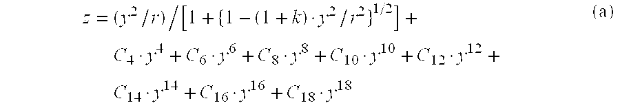
FIG. 2 is a figure showing the structure of lenses of a projection optical system according to the first preferred embodiment of the present invention. In the lenses of FIG. 2, a first lens group G1 comprises, in order from the mask side: a parallel plane plate P1; a positive meniscus lens L11 which presents its concave surface to the mask side; a positive meniscus lens L12 which presents its concave surface to the mask side; a biconvex lens L13; another biconvex lens L14; a biconcave lens L15; another biconcave lens L16; another biconcave lens L17; a biconcave lens L18 whose surface on the mask side is formed in an aspherical shape; a negative meniscus lens L19 which presents its concave surface to the mask side; a positive meniscus lens L110 which presents its concave surface which is formed in an aspherical shape to the mask side; a positive meniscus lens L111 which presents its concave surface to the mask side; another positive meniscus lens L112 which presents its concave surface to the mask side; a positive meniscus lens L113 which presents its convex surface to the mask side; another positive meniscus lens L114 which presents its convex surface to the mask side; and yet another positive meniscus lens L115 which presents its convex surface to the mask side.
Furthermore, a second lens group G2 comprises, in order from the mask side: a negative meniscus lens L21 which presents its concave surface which is formed in an aspherical shape to the wafer side; a biconcave lens L22 of which both the surface towards the mask side and the surface towards the wafer side are formed in an aspherical shape; another biconcave lens L23 of which the surface towards the mask side is formed in an aspherical shape; and a negative meniscus lens L24 which presents its convex surface which is formed in an aspherical shape to the wafer side.
Yet further, a third lens group G3 comprises, in order from the mask side: a positive meniscus lens L31 which presents its concave surface to the mask side; another positive meniscus lens L32 which presents its concave surface to the mask side; a biconvex lens L33 of which the surface towards the mask side is formed in an aspherical shape; another biconvex lens L34; a negative meniscus lens L35 which presents its concave surface to the mask side; a positive meniscus lens L36 which presents its convex surface to the mask side; another positive meniscus lens L37 which presents its convex surface to the mask side; and yet another positive meniscus lens L38 which presents its convex surface to the mask side.
Moreover, a fourth lens group G4 comprises, in order from the mask side: a positive meniscus lens L41 which presents its convex surface to the mask side; a negative meniscus lens L42 which presents its convex surface to the mask side; and a positive meniscus lens L43 which presents its convex surface to the mask side. In this first preferred embodiment of the present invention, the supply section 1 is made so as to supply water (which has an index of refraction of 1.38 at the central wavelength of 248.40 nm), and it directs a flow of water so as to fill the narrow optical path between the projection optical system 6 and the wafer 7. In other words, the projection optical system 6 of this first preferred embodiment of the present invention is made as a water immersion type optical system.
The following Table 1 specifies all the data or parameters of the projection optical system according to this first preferred embodiment of the present invention. In the main data of Table 1, λ is the central wavelength of the exposure light, β is the projection magnification, Ym is the maximum image height, NA is the image side numerical aperture, and D is the working distance. Furthermore, Table 1 shows all the optical members in order from the wafer side, and in this table: the surface number in the first column is the sequential order of the surface from the wafer side; r in the second column is the radius of curvature of each surface in mm (in the case of an aspherical surface, this is the radius of curvature of the summit); d in the third column is the gap in mm along the optical axis between the surfaces, in other words the interval between the surfaces; and n in the fourth column is the index of refraction at the central wavelength λ. It should be understood that the radius of curvature r is a positive radius of curvature for a surface which is convex towards the wafer side, and is a negative radius of curvature for a surface which is concave towards the wafer side.
| TABLE 1 |
| (Main data) |
| λ = 248.40 nm |
| β = 1/5 |
| Ym = 11.6 mm |
| NA = 0.89 |
| D = 0.5 mm |
| (Optical member data) |
| surface | ||||
| number | r | d | n | |
| (wafer surface) | ||||
| 1 | ∞ | 0.500000 | 1.38000 | (immersion liquid: water) |
| 2 | −278.38803 | 81.380761 | 1.50839 | (lens L43) |
| 3 | −144.83885 | 1.000000 | ||
| 4 | −184.30485 | 18.915187 | 1.50839 | (lens L42) |
| 5 | −704.03874 | 4.822898 | ||
| 6 | −487.23542 | 38.288622 | 1.50839 | (lens L41) |
| 7 | −163.51870 | 1.068326 | ||
| 8 | −316.44413 | 39.899826 | 1.50839 | (lens L38) |
| 9 | −173.82425 | 1.166541 | ||
| 10 | −514.79368 | 38.713118 | 1.50839 | (lens L37) |
| 11 | −256.84706 | 2.993584 | ||
| 12 | −1486.19304 | 39.000000 | 1.50839 | (lens L36) |
| 13 | −349.92079 | 5.231160 | ||
| 14 | 684.32388 | 30.000000 | 1.50839 | (lens L35) |
| 15 | 535.80500 | 16.111594 | ||
| 16 | 1423.09713 | 49.000000 | 1.50839 | (lens L34) |
| 17 | −417.61955 | 1.000000 | ||
| 18 | 534.19578 | 48.373958 | 1.50839 | (lens L33) |
| 19* | −1079.65640 | 3.793818 | ||
| 20 | 363.41400 | 41.353623 | 1.50839 | (lens L32) |
| 21 | 11327.06579 | 1.000000 | ||
| 22 | 221.09486 | 38.438778 | 1.50839 | (lens L31) |
| 23 | 576.34104 | 13.483698 | ||
| 24* | 72641.42689 | 14.000000 | 1.50839 | (lens L24) |
| 25 | 169.78783 | 36.502361 | ||
| 26 | −721.39710 | 14.000000 | 1.50839 | (lens L23) |
| 27* | 163.09868 | 55.546840 | ||
| 28* | −154.09821 | 14.000000 | 1.50839 | (lens L22) |
| 29* | 4602.19163 | 36.940676 | ||
| 30* | −162.70945 | 24.726155 | 1.50839 | (lens L21) |
| 31 | −277.47625 | 9.365299 | ||
| 32 | −233.72917 | 35.657146 | 1.50839 | (lens L115) |
| 33 | −199.92054 | 3.651342 | ||
| 34 | −760.94438 | 50.681020 | 1.50839 | (lens L114) |
| 35 | −267.98451 | 1.000000 | ||
| 36 | −8019.33680 | 51.000000 | 1.50839 | (lens L113) |
| 37 | −361.32067 | 1.000000 | ||
| 38 | 359.57299 | 51.000000 | 1.50839 | (lens L112) |
| 39 | 22205.61483 | 1.000000 | ||
| 40 | 254.06189 | 53.118722 | 1.50839 | (lens L111) |
| 41 | 814.49441 | 2.310847 | ||
| 42 | 207.87392 | 41.299164 | 1.50839 | (lens L110) |
| 43* | 325.56504 | 2.944573 | ||
| 44 | 227.90224 | 30.090705 | 1.50839 | (lens L19) |
| 45 | 176.14016 | 30.818682 | ||
| 46 | −1560.80134 | 14.019437 | 1.50839 | (lens L18) |
| 47* | 211.19874 | 18.615775 | ||
| 48 | −419.25972 | 14.000000 | 1.50839 | (lens L17) |
| 49 | 162.14317 | 19.137169 | ||
| 50 | −385.99461 | 14.000000 | 1.50839 | (lens L16) |
| 51 | 377.23568 | 16.483492 | ||
| 52 | −192.32222 | 14.000000 | 1.50839 | (lens L15) |
| 53 | 577.40909 | 1.000000 | ||
| 54 | 347.51785 | 23.387796 | 1.50839 | (lens L14) |
| 55 | −746.67387 | 1.000000 | ||
| 56 | 230.21868 | 28.789242 | 1.50839 | (lens L13) |
| 57 | −632.24530 | 1.987632 | ||
| 58 | 366.04498 | 19.840462 | 1.50839 | (lens L12) |
| 59 | 658.39254 | 1.000136 | ||
| 60 | 436.06541 | 17.664657 | 1.50839 | (lens L11) |
| 61 | 1827.22708 | 2.355320 | ||
| 62 | ∞ | 8.000000 | 1.50839 | (parallel plane plate P1) |
| 63 | ∞ | 31.664788 | ||
| (mask surface) | ||||
| (aspherical data) | |
| surface 19 | |
| k = 0.000000 | |
| C4 = 0.108661 × 10⁻¹¹ | C6 = 0.115990 × 10⁻¹³ |
| C8 = −0.252101 × 10⁻¹⁸ | C10 = 0.326093 × 10⁻²² |
| C12 = −0.249918 × 10⁻²⁶ | C14 = 0.826218 × 10⁻³¹ |
| C16 = −0.105890 × 10⁻³⁵ | C18 = 0.000000 |
| surface 24 | |
| k = 0.000000 | |
| C4 = −0.666892 × 10⁻⁸ | C6 = −0.834628 × 10⁻¹³ |
| C8 = 0.905999 × 10⁻¹⁷ | C10 = −0.275733 × 10⁻²¹ |
| C12 = −0.577535 × 10⁻²⁵ | C14 = 0.700442 × 10⁻²⁹ |
| C16 = −0.229827 × 10⁻³³ | C18 = 0.000000 |
| surface 27 | |
| k = 0.000000 | |
| C4 = 0.741662 × 10⁻⁹ | C6 = −0.603176 × 10⁻¹² |
| C8 = −0.996260 × 10⁻¹⁷ | C10 = 0.500372 × 10⁻²⁰ |
| C12 = −0.274589 × 10⁻²³ | C14 = 0.173610 × 10⁻²⁷ |
| C16 = 0.556996 × 10⁻³² | C18 = 0.000000 |
| surface 28 | |
| k = 0.000000 | |
| C4 = 0.398482 × 10⁻⁸ | C6 = 0.375195 × 10⁻¹² |
| C8 = −0.609480 × 10⁻¹⁶ | C10 = −0.178686 × 10⁻¹⁹ |
| C12 = −0.112080 × 10⁻²⁴ | C14 = −0.141732 × 10⁻²⁷ |
| C16 = 0.314821 × 10⁻³¹ | C18 = 0.000000 |
| surface 29 | |
| k = 0.000000 | |
| C4 = −0.891861 × 10⁻⁸ | C6 = 0.359788 × 10⁻¹² |
| C8 = −0.218558 × 10⁻¹⁶ | C10 = −0.633586 × 10⁻²⁰ |
| C12 = −0.317617 × 10⁻²⁴ | C14 = 0.914859 × 10⁻²⁸ |
| C16 = −0.392754 × 10⁻³² | C18 = 0.000000 |
| surface 30 | |
| k = 0.000000 | |
| C4 = 0.217828 × 10⁻⁸ | C6 = 0.199483 × 10⁻¹² |
| C8 = 0.346439 × 10⁻¹⁶ | C10 = 0.816535 × 10⁻²¹ |
| C12 = 0.143334 × 10⁻²⁴ | C14 = −0.229911 × 10⁻²⁸ |
| C16 = −0.164178 × 10⁻³² | C18 = 0.000000 |
| surface 43 | |
| k = 0.000000 | |
| C4 = 0.826617 × 10⁻⁹ | C6 = −0.152893 × 10⁻¹² |
| C8 = −0.105637 × 10⁻¹⁷ | C10 = −0.904672 × 10⁻²³ |
| C12 = −0.326047 × 10⁻²⁵ | C14 = −0.178192 × 10⁻³⁰ |
| C16 = 0.656718 × 10⁻³⁴ | C18 = 0.000000 |
| surface 47 | |
| k = 0.000000 | |
| C4 = −0.374153 × 10⁻⁷ | C6 = 0.139807 × 10⁻¹¹ |
| C8 = −0.602273 × 10⁻¹⁶ | C10 = −0.289281 × 10⁻¹⁹ |
| C12 = 0.109996 × 10⁻²² | C14 = −0.966189 × 10⁻²⁷ |
| C16 = 0.000000 | C18 = 0.000000 |
| (values in the conditions) | |
| T = 138.58 mm | |
| L = 1323.13 mm | |
| F2 = −68.34 mm | |
| (1) D = 0.5 | |
| (2) D/T = 0.003608 | |
| (3) T/L = 0.1047 | |
| (4) L = 1323.13 | |
| (5) |F2|/L = 0.05165 | |
FIG. 3 is a figure showing the coma aberration of this projection optical system according to the first preferred embodiment of the present invention. The aberration is given by the scale on the reticle side. As will be clear from this aberration figure, in this first preferred embodiment, even though the image side numerical aperture has been implemented as 0.89 which is extremely high, nevertheless it will be understood that the aberration is properly corrected.
FIG. 4 is a figure showing the structure of lenses of a projection optical system according to the second preferred embodiment of the present invention. In the lenses of FIG. 4, a first lens group G1 comprises, in order from the mask side: a parallel plane plate P1; a biconvex lens L11; another biconvex lens L12; yet another biconvex lens L13; still yet another biconvex lens L14; a negative meniscus lens L15 which presents its convex surface to the mask side; a biconvex lens L16; another biconvex lens L17; yet another biconvex lens L18; a negative meniscus lens L19 which presents its concave surface to the mask side; a positive meniscus lens L110 which presents its concave surface to the mask side; another positive meniscus lens L111 which presents its concave surface to the mask side; a biconvex lens L112; another biconvex lens L113; a positive meniscus lens L114 which presents its convex surface to the mask side; and another positive meniscus lens L115 which presents its convex surface to the mask side.
Furthermore, a second lens group G2 comprises, in order from the mask side: a negative meniscus lens L21 which presents its convex surface to the mask side; a negative meniscus lens L22 which whose concave surface on the wafer side is formed in an aspherical shape; a biconvex lens L23 whose surface on the mask side is formed in an aspherical shape; and a negative meniscus lens L24 whose convex surface on the wafer side is formed in an aspherical shape.
Yet further, a third lens group G3 comprises, in order from the mask side: a positive meniscus lens L31 which presents its concave surface to the mask side; a biconvex lens L32; another biconvex lens L33; yet another biconvex lens L34; a negative meniscus lens L35 whose concave surface on the mask side is formed in an aspherical shape; a positive meniscus lens L36 which presents its convex surface to the mask side; another positive meniscus lens L37 which presents its convex surface to the mask side; and yet another positive meniscus lens L38 which presents its convex surface to the mask side.
Finally, a fourth lens group G4 comprises, in order from the mask side: a positive meniscus lens L41 which presents its convex surface to the mask side; a negative meniscus lens L42 which presents its convex surface to the mask side; and a positive meniscus lens L43 which presents its convex surface to the mask side. In this second preferred embodiment of the present invention, the supply section 10 is made so as to supply air, so that a flow of air is generated in the narrow optical path between the projection optical system 6 and the wafer 7. It should be understood that, since the refractive index of air is 1.0, it is omitted from Table 1 and Table 2.
In the following Table 2, the various data or parameters of the projection optical system according to this second preferred embodiment of the present invention are detailed. In the main data of Table 2, λ is the central wavelength of the exposure light, β is the projection magnification, Ym is the maximum image height, NA is the image side numerical aperture, and D is the working distance. Furthermore, Table 2 shows all the optical members, and in this table: the surface number in the first column is the sequential order of the surface from the wafer side; r in the second column is the radius of curvature of each surface in mm (in the case of an aspherical surface, this is the radius of curvature of the summit); d in the third column is the gap in mm along the optical axis between the surfaces, in other words the interval between the surfaces; and n in the fourth column is the index of refraction at the central wavelength λ. It should be understood that the radius of curvature r is a positive radius of curvature for a surface which is convex towards the wafer side, and is a negative radius of curvature for a surface which is concave towards the wafer side.
| TABLE 2 |
| (Main data) |
| λ = 248.40 nm |
| β = 1/5 |
| Ym = 11.6 mm |
| NA = 0.88 |
| D = 2.5 mm |
| (Optical member data) |
| Surface | ||||
| number | r | d | n | |
| (wafer surface) | ||||
| 1 | ∞ | 2.500000 | ||
| 2 | −1270.40584 | 77.251684 | 1.50839 | (lens L43) |
| 3 | −110.72777 | 1.000000 | ||
| 4 | −132.78132 | 18.339030 | 1.50839 | (lens L42) |
| 5 | −1152.71012 | 4.938823 | ||
| 6 | −723.27523 | 38.179053 | 1.50839 | (lens L41) |
| 7 | −181.43794 | 1.050956 | ||
| 8 | −297.93827 | 41.055103 | 1.50839 | (lens L38) |
| 9 | −166.87288 | 2.382931 | ||
| 10 | −427.65954 | 40.104060 | 1.50839 | (lens L37) |
| 11 | −244.29595 | 4.903887 | ||
| 12 | −3387.32378 | 39.000000 | 1.50839 | (lens L36) |
| 13 | −420.50275 | 7.614732 | ||
| 14 | 540.89354 | 29.000000 | 1.50839 | (lens L35) |
| 15* | 474.45854 | 15.158591 | ||
| 16 | 897.00143 | 50.000000 | 1.50839 | (lens L34) |
| 17 | −506.01529 | 1.138429 | ||
| 18 | 570.25291 | 48.910744 | 1.50839 | (lens L33) |
| 19 | −952.62514 | 5.055203 | ||
| 20 | 378.82882 | 43.067991 | 1.50839 | (lens L32) |
| 21 | −78415.53819 | 1.000000 | ||
| 22 | 258.78592 | 40.107177 | 1.50839 | (lens L31) |
| 23 | 1095.44138 | 10.651612 | ||
| 24* | 4500.00000 | 14.000000 | 1.50839 | (lens L24) |
| 25 | 189.07807 | 34.499414 | ||
| 26 | −808.48380 | 14.000000 | 1.50839 | (lens L23) |
| 27* | 177.87730 | 56.721169 | ||
| 28* | −143.78515 | 14.000000 | 1.50839 | (lens L22) |
| 29 | −2706.72147 | 35.781478 | ||
| 30 | −159.97919 | 24.199673 | 1.50839 | (lens L21) |
| 31 | −298.84455 | 8.626663 | ||
| 32 | −239.84826 | 35.242789 | 1.50839 | (lens L115) |
| 33 | −180.77301 | 1.706975 | ||
| 34 | −521.24921 | 49.373247 | 1.50839 | (lens L114) |
| 35 | −258.27460 | 1.000000 | ||
| 36 | 8792.77756 | 51.000000 | 1.50839 | (lens L113) |
| 37 | −481.86914 | 1.000000 | ||
| 38 | 336.67038 | 51.000000 | 1.50839 | (lens L112) |
| 39 | 1368401.4891 | 5.064530 | ||
| 40 | 261.20998 | 49.550014 | 1.50839 | (lens L111) |
| 41 | 1066.67182 | 2.872022 | ||
| 42 | 222.75670 | 41.276937 | 1.50839 | (lens L110) |
| 43 | 309.81127 | 2.988277 | ||
| 44 | 224.97144 | 30.049724 | 1.50839 | (lens L19) |
| 45 | 178.92869 | 24.175760 | ||
| 46 | −4551.95559 | 14.140578 | 1.50839 | (lens L18) |
| 47 | 163.47384 | 23.589033 | ||
| 48 | −435.59405 | 14.000000 | 1.50839 | (lens L17) |
| 49 | 212.20765 | 20.350602 | ||
| 50 | −255.41661 | 14.000000 | 1.50839 | (lens L16) |
| 51 | 476.81062 | 19.854085 | ||
| 52 | −166.35775 | 14.000000 | 1.50839 | (lens L15) |
| 53 | −3092.07241 | 1.000000 | ||
| 54 | 1013.37837 | 21.280878 | 1.50839 | (lens L14) |
| 55 | −649.18244 | 14.095688 | ||
| 56 | 562.23230 | 28.026479 | 1.50839 | (lens L13) |
| 57 | −495.38628 | 1.000000 | ||
| 58 | 400.84453 | 30.179322 | 1.50839 | (lens L12) |
| 59 | −861.42926 | 1.000000 | ||
| 60 | 1152.72543 | 51.631197 | 1.50839 | (lens L11) |
| 61 | −1403.48221 | 1.000057 | ||
| 62 | ∞ | 8.000000 | 1.50839 | (parallel plane plate P1) |
| 63 | ∞ | 59.860116 | ||
| (mask surface) | ||||
| (aspherical data) | |
| surface 15 | |
| k = 0.135621 | |
| C4 = 0.132068 × 10⁻⁹ | C6 = 0.254077 × 10⁻¹⁴ |
| C8 = 0.520547 × 10⁻¹⁸ | C10 = −0.100941 × 10⁻²² |
| C12 = 0.104925 × 10⁻²⁷ | C14 = 0.102740 × 10⁻³¹ |
| C16 = −0.510544 × 10−36 | C18 = 0.909690 × 10−41 |
| surface 24 | |
| k = 0.000000 | |
| C4 = −0.757298 × 10⁻⁸ | C6 = −0.194318 × 10⁻¹² |
| C8 = 0.114312 × 10⁻¹⁶ | C10 = 0.325024 × 10⁻²¹ |
| C12 = −0.811964 × 10⁻²⁵ | C14 = 0.733478 × 10⁻²⁹ |
| C16 = −0.344978 × 10⁻³³ | C18 = 0.593551 × 10−38 |
| surface 27 | |
| k = 0.000000 | |
| C4 = 0.274792 × 10⁻⁸ | C6 = −0.591295 × 10⁻¹² |
| C8 = −0.101460 × 10⁻¹⁶ | C10 = 0.649406 × 10⁻²⁰ |
| C12 = −0.146673 × 10⁻²³ | C14 = 0.199948 × 10⁻²⁷ |
| C16 = −0.110641 × 10⁻³¹ | C18 = 0.153140 × 10−36 |
| surface 28 | |
| k = 0.000000 | |
| C4 = 0.181334 × 10⁻⁸ | C6 = 0.386127 × 10⁻¹² |
| C8 = 0.250729 × 10⁻¹⁶ | C10 = −0.340803 × 10⁻²⁰ |
| C12 = 0.956332 × 10⁻²⁴ | C14 = −0.123696 × 10⁻²⁷ |
| C16 = 0.102868 × 10⁻³¹ | C18 = −0.312692 × 10−36 |
| (values in the conditions) | |
| T = 133.77 mm | |
| L = 1407.55 mm | |
| F2 = −72.10 mm | |
| (1) D = 2.5 | |
| (2) D/T = 0.01869 | |
| (3) T/L = 0.09504 | |
| (4) L = 1407.55 | |
| (5) |F2|/L = 0.05122 | |
FIG. 5 is a figure showing the coma aberration of this projection optical system according to the second preferred embodiment of the present invention. The aberration is given by the scale on the reticle side. As will be clear from this aberration figure, in this second preferred embodiment, even though the image side numerical aperture has been implemented as 0.88 which is extremely high, nevertheless it will be understood that the aberration is properly corrected.
FIG. 6 is a figure showing the structure of lenses of a projection optical system according to the third preferred embodiment of the present invention. In the lens of FIG. 6, a first lens group G1 comprises, in order from the mask side: a biconcave lens L11; a biconvex lens L12; another biconvex lens L13; a positive meniscus lens L14 which presents its convex surface to the mask side; a negative meniscus lens L15 which presents its convex surface to the mask side; a biconcave lens L16; another biconcave lens L17; a positive meniscus lens L18 which presents its concave surface to the mask side; a biconvex lens L19; another biconvex lens L20; a positive meniscus lens L21 which presents its convex surface to the mask side; and another positive meniscus lens L22 which presents its convex surface to the mask side.
Furthermore, a second lens group G2 comprises, in order from the mask side: a negative meniscus lens L23 which presents its convex surface to the mask side; another negative meniscus lens L24 which presents its convex surface to the mask side; a biconcave lens L25; and a negative meniscus lens L26 which presents its concave surface to the mask side.
Yet further, a third lens group G3 comprises, in order from the mask side: a positive meniscus lens L27 which presents its concave surface to the mask side; a biconvex lens L28; another biconvex lens L29; a negative meniscus lens L30 which presents its convex surface to the mask side; a biconvex lens L31; and a positive meniscus lens L32 which presents its convex surface to the mask side.
Finally, a fourth lens group G4 comprises, in order from the mask side: a positive meniscus lens L33 which presents its convex surface to the mask side; another positive meniscus lens L34 which presents its convex surface to the mask side; yet another positive meniscus lens L35 which presents its convex surface to the mask side; and a parallel plane plate P1.
In the following Table 3, the various data or parameters of the projection optical system according to this third preferred embodiment of the present invention are detailed. In the main data of Table 3, λ is the central wavelength of the exposure light, β is the projection magnification, Ym is the maximum image height, NA is the image side numerical aperture, and D is the working distance. Furthermore, Table 3 shows all the optical members, and in this table: the surface number in the first column is the sequential order of the surface from the wafer side; r in the second column is the radius of curvature of each surface in mm (in the case of an aspherical surface, this is the radius of curvature of the summit); d in the third column is the gap in mm along the optical axis between the surfaces, in other words the interval between the surfaces; and n in the fourth column is the index of refraction at the central wavelength λ. It should be understood that the radius of curvature r is a positive radius of curvature for a surface which is convex towards the wafer side, and is a negative radius of curvature for a surface which is concave towards the wafer side.
| TABLE 3 |
| (Main data) |
| λ = 193.31 nm |
| β = 1/4 |
| Ym = 11.6 mm |
| NA = 0.85 |
| D = 4.8 mm |
| (Optical member data) |
| n = 1.560353 (quartz), n = 1.501474 (fluor) |
| Surface | ||||
| number | r | d | n | |
| (wafer surface) | ||||
| 1 | ∞ | 4.800000 | ||
| 2 | ∞ | 4.000000 | 1.501474 | (parallel plane plate P1) |
| 3 | ∞ | 1.516803 | ||
| 4 | −347.07689 | 59.005134 | 1.560353 | (lens L35) |
| 5* | −147.42602 | 24.672134 | ||
| 6 | −155.30862 | 36.048560 | 1.560353 | (lens L34) |
| 7* | −127.29829 | 3.818982 | ||
| 8 | −495.00000 | 41.252390 | 1.560353 | (lens L33) |
| 9 | −186.65984 | 1.837210 | ||
| 10 | −8649.91361 | 41.354410 | 1.560353 | (lens L32) |
| 11 | −338.42422 | 7.812864 | ||
| 12 | 3117.31974 | 56.482714 | 1.501474 | (lens L31) |
| 13 | −242.28533 | 6.259672 | ||
| 14 | −219.07804 | 22.000000 | 1.560353 | (lens L30) |
| 15 | −295.48408 | 1.000000 | ||
| 16 | 982.58745 | 35.100000 | 1.560353 | (lens L29) |
| 17 | −717.19251 | 1.027505 | ||
| 18* | 345.99292 | 35.100000 | 1.501474 | (lens L28) |
| 19 | −1657.34210 | 4.870546 | ||
| 20 | 170.09691 | 43.238577 | 1.501474 | (lens L27) |
| 21* | 1247.60125 | 3.728285 | ||
| 22 | 2570.01253 | 12.600000 | 1.560353 | (lens L26) |
| 23* | 140.20387 | 38.046549 | ||
| 24 | −302.07583 | 9.000000 | 1.560353 | (lens L25) |
| 25 | 174.63448 | 47.228736 | ||
| 26* | −110.02031 | 11.990000 | 1.560353 | (lens L24) |
| 27 | −227.61981 | 19.287967 | ||
| 28 | −145.96360 | 13.625000 | 1.560353 | (lens L23) |
| 29 | −993.54187 | 2.180979 | ||
| 30 | −926.50000 | 49.004494 | 1.501474 | (lens L22) |
| 31 | −211.89314 | 1.805004 | ||
| 32 | −1634.25815 | 46.870000 | 1.560353 | (lens L21) |
| 33 | −309.72040 | 1.090000 | ||
| 34 | 1870.87868 | 44.992783 | 1.560353 | (lens L20) |
| 35 | −397.39272 | 1.090000 | ||
| 36 | 310.83083 | 46.730190 | 1.560353 | (lens L19) |
| 37 | −12381.83318 | 1.065257 | ||
| 38 | 219.21300 | 43.890391 | 1.560353 | (lens L18) |
| 39 | 459.28473 | 62.355122 | ||
| 40* | −1607.04793 | 23.010030 | 1.560353 | (lens L17) |
| 41* | 210.26262 | 27.392360 | ||
| 42 | −182.19964 | 11.990000 | 1.560353 | (lens L16) |
| 43 | 397.04358 | 31.491045 | ||
| 44 | −126.09618 | 12.834065 | 1.560353 | (lens L15) |
| 45 | −4686.72757 | 31.683354 | ||
| 46 | −7627.00504 | 35.000000 | 1.560353 | (lens L14) |
| 47 | −178.80540 | 1.090000 | ||
| 48 | 362.15153 | 35.000000 | 1.560353 | (lens L13) |
| 49 | −434.88773 | 1.000000 | ||
| 50 | 217.92403 | 34.335000 | 1.560353 | (lens L12) |
| 51 | −854.29087 | 44.741881 | ||
| 52 | −293.27068 | 11.083963 | 1.560353 | (lens L11) |
| 53 | 198.96759 | 58.442143 | ||
| (mask surface) | ||||
| (aspherical data) | |
| surface 5 | |
| k = 0.000000 | |
| C4 = −0.717239 × 10−08 | C6 = −0.101122 × 10⁻¹¹ |
| C8 = 0.181395 × 10⁻¹⁶ | C10 = 0.626626 × 10⁻²⁰ |
| C12 = 0.124335 × 10⁻²³ | C14 = 0.306352 × 10⁻²⁷ |
| C16 = −0.451516 × 10⁻³¹ | C18 = 0.000000 |
| surface 7 | |
| k = 0.000000 | |
| C4 = −0.171015 × 10−09 | C6 = −0.130062 × 10⁻¹² |
| C8 = −0.919066 × 10⁻¹⁷ | C10 = −0.567556 × 10⁻²² |
| C12 = 0.169635 × 10⁻²⁵ | C14 = 0.232608 × 10⁻³⁰ |
| C16 = 0.300428 × 10⁻³⁵ | C18 = 0.285031 × 10−38 |
| surface 18 | |
| k = 0.000000 | |
| C4 = 0.360694 × 10−09 | C6 = 0.338660 × 10⁻¹³ |
| C8 = 0.880881 × 10⁻¹⁸ | C10 = −0.289409 × 10⁻²² |
| C12 = −0.909784 × 10⁻²⁷ | C14 = 0.759036 × 10⁻³¹ |
| C16 = −0.400220 × 10⁻³⁵ | C18 = 0.235613 × 10−39 |
| surface 21 | |
| k = 0.000000 | |
| C4 = −0.139770 × 10−08 | C6 = −0.642555 × 10⁻¹³ |
| C8 = 0.410206 × 10⁻¹⁷ | C10 = 0.559358 × 10⁻²¹ |
| C12 = −0.314678 × 10⁻²⁵ | C14 = −0.577909 × 10⁻³⁰ |
| C16 = 0.154846 × 10⁻³³ | C18 = −0.130804 × 10−37 |
| surface 23 | |
| k = 0.000000 | |
| C4 = −0.206235 × 10−08 | C6 = −0.790155 × 10⁻¹³ |
| C8 = −0.830872 × 10⁻¹⁷ | C10 = −0.678238 × 10⁻²⁰ |
| C12 = −0.145920 × 10⁻²³ | C14 = −0.234851 × 10⁻²⁸ |
| C16 = 0.259860 × 10⁻³¹ | C18 = −0.223564 × 10⁻³⁵ |
| surface 26 | |
| k = 0.000000 | |
| C4 = 0.226273 × 10−08 | C6 = −0.406498 × 10⁻¹² |
| C8 = −0.357047 × 10⁻¹⁷ | C10 = −0.897263 × 10⁻²¹ |
| C12 = −0.510647 × 10⁻²⁴ | C14 = −0.322709 × 10⁻²⁹ |
| C16 = 0.480022 × 10⁻³² | C18 = −0.529104 × 10−36 |
| surface 40 | |
| k = 0.000000 | |
| C4 = −0.309170 × 10−08 | C6 = −0.215102 × 10⁻¹² |
| C8 = −0.403443 × 10⁻¹⁶ | C10 = 0.485396 × 10⁻²⁰ |
| C12 = 0.676821 × 10⁻²⁵ | C14 = −0.456289 × 10⁻²⁸ |
| C16 = 0.323963 × 10⁻³¹ | C18 = −0.337348 × 10−36 |
| surface 41 | |
| k = 0.000000 | |
| C4 = −0.156117 × 10−07 | C6 = 0.118556 × 10⁻¹¹ |
| C8 = −0.440276 × 10⁻¹⁶ | C10 = −0.123461 × 10⁻¹⁹ |
| C12 = 0.933626 × 10⁻²⁴ | C14 = 0.134725 × 10⁻²⁷ |
| C16 = −0.261036 × 10⁻³¹ | C18 = 0.000000 |
| (values in the conditions) | |
| T = 172.15 mm | |
| L = 1246.87 mm | |
| F2 = −49.585 mm | |
| (1) D = 4.8 | |
| (2) D/T = 0.02788 | |
| (3) T/L = 0.13807 | |
| (4) L = 1246.87 | |
| (5) |F2|/L = 0.03977 | |
FIG. 7 is a figure showing the coma aberration of this projection optical system according to the third preferred embodiment of the present invention. The coma aberration is given by the scale on the reticle side. As will be clear from this aberration figure, in this third preferred embodiment, even though the image side numerical aperture has been implemented as 0.85 which is quite high, nevertheless it will be understood that the aberration is properly corrected.
As described above, with the projection optical systems according to the various preferred embodiments of the present invention explained above, it is possible to keep the image side numerical aperture extremely high, along with restraining increase of the lens outer diameter. Accordingly, with the exposure apparatuses according to the first and second preferred embodiments of the present invention explained above, it is possible to perform projection exposure at high accuracy using a projection optical system of high resolution, based upon the use of KrF excimer laser beams. Furthermore, with the exposure apparatus according to the third preferred embodiment as described above, it is likewise possible to perform projection exposure at high accuracy using a projection optical system of high resolution, based upon the use of ArF excimer laser beams.
With the exposure apparatus according to the present invention as described above, it is possible to manufacture a microdevice (such as a semiconductor element, an image capturing element, a liquid crystal display element, a thin film magnetic head or the like) by illuminating the mask (reticle) via the illumination optical system (a so called illumination process), and by exposing a pattern which is formed upon the mask and which is to be transferred onto a photosensitive substrate via the projection optical system (a so called exposure process). In the following, an example of the procedure utilized when producing a micro device, which in this case is a semiconductor device, by forming a predetermined circuit pattern upon a wafer or the like, which serves as the photosensitive substrate, using the exposure apparatus according to the present invention as described above, will be explained with reference to the flow chart of FIG. 8.
First, in a step 301 of FIG. 8, a metallic layer is formed by vapor deposition upon a wafer in one lot Next, in a step 302, a photoresist is coated upon this metallic layer upon the wafer in one lot. After this, in a step 303, an image of a pattern upon a mask is exposed and transferred onto each shot region upon this wafer in one lot in order, using an exposure apparatus according to any of the preferred embodiments of the present invention as described above, via the projection optical system of this exposure apparatus. After this, in a step 304, the photoresist upon this wafer in one lot is developed, and then in a step 305 etching is performed upon the wafer in one lot with this resist pattern as a mask, so that a circuit pattern is formed upon each shot region of the wafer corresponding to the pattern upon the mask. After this, devices such as semiconductor elements or the like are manufactured by forming circuit patterns on further upper layers or the like. According to the above described method of semiconductor device manufacture, it is possible to obtain semiconductor devices having an extremely minute circuit pattern with good throughput.
Furthermore it is possible, by utilizing the exposure apparatus according to the present invention as described above, to obtain a microdevice, which in this case is a liquid crystal display element, by forming predetermined patterns (a circuit pattern, an electrode pattern, and the like) upon a plate (a glass substrate). In the following, an example of the procedure utilized in this case will be explained with reference to the flow chart of FIG. 9. Referring to this figure, first in a pattern formation process 401 a so called photolithography process is performed by exposing and transferring an image of a pattern upon a mask onto a photosensitive substrate (a glass substrate or the like which is coated with a resist), using an exposure apparatus according to any of the preferred embodiments of the present invention as described above, via the projection optical system of this exposure apparatus. A predetermined pattern including a large number of electrodes or the like is formed upon the photosensitive substrate by this photolithography process. After this, various processes such as a development process, an etching process, a resist removing process and the like are performed upon this substrate which has been exposed, so that the predetermined pattern is formed upon the substrate, and next a color filter formation process 402 is started.
In this color filter formation process 402, a color filter is formed in which a large number of groups of three dots which correspond to R (red), G (green), and B (blue) are arranged in a matrix pattern, or a plurality of groups of three R, G, and B filter stripes are arranged in the horizontal scan line direction. And after this color filter formation process, a cell assembly process 403 is performed. In this cell assembly process, a liquid crystal panel (liquid crystal cell) is assembled using the substrate having the predetermined pattern which was produced in the pattern formation process 401, and the color filter which was produced in the color filter formation process 402. In this cell assembly process, for example, a quantity of liquid crystal material is introduced between the substrate having the predetermined pattern which was produced in the pattern formation process 401, and the color filter which was produced in the color filter formation process 402, and thereby a liquid crystal panel (a liquid crystal cell) is manufactured.
After this, in a module assembly process 404, various further elements such as an electrical circuit which performs display operation for this liquid crystal panel (liquid crystal cell) which has been thus assembled, a backlight, and the like are fitted thereto, and thereby the manufacture of the liquid crystal display element is completed. It is possible to manufacture liquid crystal display elements having an extremely fine circuit pattern with good throughput, according to the above described method for liquid crystal display element manufacture.
It should be understood that, although the above explanation of various preferred embodiments of the present invention was made in terms of the use of a KrF excimer laser light source as the light source, this is not to be considered as being limitative of the present invention; for example, it would also be possible to utilize an ArF excimer laser light source (of wavelength 193 nm) as the light source; and other suitable possibilities could also be exploited.
Furthemore, although the above explanation of various preferred embodiments of the projection optical system of the present invention was made, by way of example, in terms of the projection optical system being fitted to an exposure apparatus, it will be clearly understood that it is possible to apply the present invention to any projection optical system for forming an image of a first object upon a second object.
Claims (11)
1. A projection optical system whose image side numerical aperture is greater than or equal to 0.75, and which forms an image of a first object upon a second object using light of a predetermined wavelength less than or equal to 300 nm, comprising:
a first lens group G1 of positive refractive power;
a second lens group G2 of negative refractive power;
a third lens group G3 of positive refractive power; and
a fourth lens group G4 of positive refractive power, wherein:
the first lens group G1, the second lens group G2, the third lens group G3 and the fourth lens group G4 are arranged in order from a side of the first object; and
a distance D in mm along an optical axis between an optical surface of the fourth lens group G4 closest to the second object, and the second object, satisfies a condition of 0.1<D<5.
2. A projection optical system according to claim 1 , wherein the projection optical system has an image side numerical aperture greater than or equal to 0.8.
3. A projection optical system according to claim 1 , wherein, with T being a sum of thicknesses along the optical axis of all optical members included in the fourth lens group G4, and with D being the distance along the optical axis between the optical surface of the fourth lens group G4 closest to the second object, and the second object, a condition of 0.001<D/T<0.2 is satisfied.
4. A projection optical system according to claim 1 , wherein, with T being a sum of the thicknesses along the optical axis of all optical members included in the fourth lens group G4, and with L being a distance along the optical axis between the first object and the second object, a condition of 0.02<T/L is satisfied.
5. A projection optical system according to claim 1 , wherein a distance L in mm along the optical axis between the first object and the second object satisfies a condition of 800<L<1600.
6. A projection optical system according to claim 1 , wherein a focal length F2 of the second lens group G2 and a distance L in mm along the optical axis between the first object and the second object satisfy a condition of 0.01<|F2|/L<0.15.
7. A projection optical system according to claim 1 , wherein at least one of a plurality of optical surfaces comprised in the projection optical system is formed in an aspherical shape.
8. An exposure apparatus, comprising:
an illumination system for illuminating a mask as a first object;
a projection optical system according to claim 1 , that forms an image of a pattern which is formed upon the mask upon a photosensitive substrate as the second object; and
a prevention device that prevents gas which is generated from the photosensitive substrate from adhering to the optical surface closest to the second object of the fourth lens group G4 of the projection optical system.
9. An exposure apparatus according to claim 8 , wherein the prevention device comprises a flow forming device that forms a predetermined flow of gas or liquid in a optical path between the optical surface closest to the second object of the fourth lens group G4 and the photosensitive substrate.
10. An exposure method, comprising:
an illumination process of illuminating a mask as a first object; and
an exposure process of exposing, via a projection optical system according to claim 1 , an image of a pattern which is formed upon the mask upon a photosensitive substrate as the second object, wherein
the exposure process comprises a flow formation process of forming a predetermined flow of gas or liquid in a optical path between the optical surface closest to the second object of the fourth lens group G4 and the photosensitive substrate, in order to prevent gas which is generated from the photosensitive substrate from adhering to the optical surface closest to the second object of the fourth lens group G4.
11. A method for manufacturing a microdevice, comprising:
an exposure process of exposing a pattern on a mask upon a photosensitive substrate, using an exposure method according to claim 10 ; and
a development process of developing the photosensitive substrate which has been exposed by the exposure process.
Priority Applications (2)
| Application Number | Priority Date | Filing Date | Title |
|---|---|---|---|
| US10/628,744 US6844919B2 (en) | 2000-12-11 | 2003-07-30 | Projection optical system and exposure apparatus having the projection optical system |
| US10/925,965 US20050024617A1 (en) | 2000-12-11 | 2004-08-26 | Projection optical system and exposure apparatus having the projection optical system |
Applications Claiming Priority (2)
| Application Number | Priority Date | Filing Date | Title |
|---|---|---|---|
| JP2000375992 | 2000-12-11 | ||
| JP2000-375992 | 2000-12-11 |
Related Child Applications (1)
| Application Number | Title | Priority Date | Filing Date |
|---|---|---|---|
| US10/628,744 Continuation US6844919B2 (en) | 2000-12-11 | 2003-07-30 | Projection optical system and exposure apparatus having the projection optical system |
Publications (2)
| Publication Number | Publication Date |
|---|---|
| US20030030916A1 US20030030916A1 (en) | 2003-02-13 |
| US6633365B2 true US6633365B2 (en) | 2003-10-14 |
Family
ID=18844916
Family Applications (3)
| Application Number | Title | Priority Date | Filing Date |
|---|---|---|---|
| US10/006,667 Expired - Lifetime US6633365B2 (en) | 2000-12-11 | 2001-12-10 | Projection optical system and exposure apparatus having the projection optical system |
| US10/628,744 Expired - Fee Related US6844919B2 (en) | 2000-12-11 | 2003-07-30 | Projection optical system and exposure apparatus having the projection optical system |
| US10/925,965 Abandoned US20050024617A1 (en) | 2000-12-11 | 2004-08-26 | Projection optical system and exposure apparatus having the projection optical system |
Family Applications After (2)
| Application Number | Title | Priority Date | Filing Date |
|---|---|---|---|
| US10/628,744 Expired - Fee Related US6844919B2 (en) | 2000-12-11 | 2003-07-30 | Projection optical system and exposure apparatus having the projection optical system |
| US10/925,965 Abandoned US20050024617A1 (en) | 2000-12-11 | 2004-08-26 | Projection optical system and exposure apparatus having the projection optical system |
Country Status (3)
| Country | Link |
|---|---|
| US (3) | US6633365B2 (en) |
| KR (1) | KR100866818B1 (en) |
| TW (1) | TW512237B (en) |
Cited By (98)
| Publication number | Priority date | Publication date | Assignee | Title |
|---|---|---|---|---|
| US20040114117A1 (en) * | 2002-11-18 | 2004-06-17 | Asml Netherlands B.V. | Lithographic apparatus and device manufacturing method |
| US20040135099A1 (en) * | 2002-11-29 | 2004-07-15 | Asml Netherlands B.V. | Lithographic apparatus and device manufacturing method |
| US20040136494A1 (en) * | 2002-11-12 | 2004-07-15 | Asml Netherlands B.V. | Lithographic apparatus and device manufacturing method |
| US20040160582A1 (en) * | 2002-11-12 | 2004-08-19 | Asml Netherlands B.V. | Lithographic apparatus and device manufacturing method |
| US20040207824A1 (en) * | 2002-11-12 | 2004-10-21 | Asml Netherlands B.V. | Lithographic apparatus and device manufacturing method |
| WO2004095135A3 (en) * | 2003-04-17 | 2004-12-09 | Nippon Kogaku Kk | Optical arrangement of autofocus elements for use with immersion lithography |
| US20050002004A1 (en) * | 2003-06-27 | 2005-01-06 | Asml Nitherlands B.V. | Lithographic apparatus and device manufacturing method |
| US20050007570A1 (en) * | 2003-05-30 | 2005-01-13 | Asml Netherlands B.V. | Lithographic apparatus and device manufacturing method |
| US20050018155A1 (en) * | 2003-06-27 | 2005-01-27 | Asml Netherlands B. V. | Lithographic apparatus and device manufacturing method |
| US20050018156A1 (en) * | 2003-06-30 | 2005-01-27 | Asml Netherlands B.V. | Lithographic apparatus and device manufacturing method |
| US20050024609A1 (en) * | 2003-06-11 | 2005-02-03 | Asml Netherlands B.V. | Lithographic apparatus and device manufacturing method |
| US20050030501A1 (en) * | 2003-06-30 | 2005-02-10 | Asml Netherlands B.V. | Lithographic apparatus and device manufacturing method |
| US20050030498A1 (en) * | 2003-07-28 | 2005-02-10 | Asml Netherlands B.V. | Lithographic projection apparatus and device manufacturing method |
| US20050036121A1 (en) * | 2002-11-12 | 2005-02-17 | Asml Netherlands B.V. | Lithographic apparatus and device manufacturing method |
| US20050042554A1 (en) * | 2003-07-28 | 2005-02-24 | Asml Netherlands B.V. | Lithographic apparatus, device manufacturing method and a substrate |
| US20050041225A1 (en) * | 2003-07-24 | 2005-02-24 | Asml Netherlands B.V. | Lithographic apparatus and device manufacturing method |
| US20050046813A1 (en) * | 2003-07-16 | 2005-03-03 | Asmil Netherlands B.V. | Lithographic apparatus and device manufacturing method |
| US20050048220A1 (en) * | 2003-07-31 | 2005-03-03 | Asml Netherlands B.V. | Lithographic apparatus and device manufacturing method |
| US20050088635A1 (en) * | 2003-09-29 | 2005-04-28 | Asml Netherlands B.V. | Lithographic apparatus and device manufacturing method |
| US20050094114A1 (en) * | 2003-09-29 | 2005-05-05 | Asml Netherlands B.V. | Lithographic apparatus and device manufacturing method |
| US20050094116A1 (en) * | 2003-08-29 | 2005-05-05 | Asml Netherlands B.V. | Gradient immersion lithography |
| US20050110973A1 (en) * | 2003-11-24 | 2005-05-26 | Asml Netherlands B.V. | Lithographic apparatus and device manufacturing method |
| US20050128445A1 (en) * | 2003-10-28 | 2005-06-16 | Asml Netherlands B.V. | Lithographic apparatus and device manufacturing method |
| US20050132914A1 (en) * | 2003-12-23 | 2005-06-23 | Asml Netherlands B.V. | Lithographic apparatus, alignment apparatus, device manufacturing method, and a method of converting an apparatus |
| US20050134815A1 (en) * | 2003-12-23 | 2005-06-23 | Asml Netherlands B.V. | Lithographic apparatus and device manufacturing method |
| US20050168713A1 (en) * | 2003-06-19 | 2005-08-04 | Asml Holding N.V. | Immersion photolithography system and method using microchannel nozzles |
| US20050174550A1 (en) * | 2003-10-15 | 2005-08-11 | Asml Netherlands B.V. | Lithographic apparatus and device manufacturing method |
| US20050175940A1 (en) * | 2004-02-11 | 2005-08-11 | Asml Netherlands B.V. | Device manufacturing method and a substrate |
| US20050179877A1 (en) * | 2003-10-15 | 2005-08-18 | Asml Netherlands B.V. | Lithographic apparatus and device manufacturing method |
| US20050219481A1 (en) * | 2004-04-02 | 2005-10-06 | Asml Netherlands B.V. | Lithographic apparatus and device manufacturing method |
| US20050219489A1 (en) * | 2002-12-10 | 2005-10-06 | Nikon Corporation | Exposure apparatus and method for producing device |
| US20050219482A1 (en) * | 2004-04-01 | 2005-10-06 | Asml Netherlands B.V. | Lithographic apparatus, device manufacturing method and device manufactured thereby |
| US20050219499A1 (en) * | 2004-04-01 | 2005-10-06 | Asml Netherlands B.V. | Lithographic apparatus and device manufacturing method |
| US20050225737A1 (en) * | 2003-12-19 | 2005-10-13 | Carl Zeiss Smt Ag | Projection objective for immersion lithography |
| US20050231814A1 (en) * | 2002-03-08 | 2005-10-20 | Carl Zeiss Smt Ag | Refractive projection objective for immersion lithography |
| US20050231694A1 (en) * | 2004-04-14 | 2005-10-20 | Asml Netherlands B.V. | Lithographic apparatus and device manufacturing method |
| US20050243292A1 (en) * | 2004-05-03 | 2005-11-03 | Asml Netherlands B.V. | Lithographic apparatus and device manufacturing method |
| US20050254031A1 (en) * | 2003-06-27 | 2005-11-17 | Asml Holding N.V. | Immersion photolithography system and method using inverted wafer-projection optics interface |
| US20050259233A1 (en) * | 2004-05-21 | 2005-11-24 | Asml Netherlands B.V. | Lithographic apparatus and device manufacturing method |
| US20050259236A1 (en) * | 2003-09-29 | 2005-11-24 | Asml Netherlands B.V. | Lithographic apparatus and device manufacturing method |
| US20050259232A1 (en) * | 2004-05-18 | 2005-11-24 | Asml Netherlands B.V. | Lithographic apparatus and device manufacturing method |
| US20050264778A1 (en) * | 2003-06-09 | 2005-12-01 | Asml Netherlands B.V. | Lithographic apparatus and device manufacturing method |
| US20050263068A1 (en) * | 2003-10-28 | 2005-12-01 | Asml Netherlands B.V. | Lithographic apparatus |
| US20050273590A1 (en) * | 2004-06-04 | 2005-12-08 | Asustek Computer Inc. | Multiple over-clocking main board and control method thereof |
| US20060007558A1 (en) * | 2004-07-06 | 2006-01-12 | Tadashi Hirata | Liquid-immersion objective optical system |
| US20060007421A1 (en) * | 2003-10-31 | 2006-01-12 | Asml Netherlands B.V. | Lithographic apparatus and device manufacturing method |
| US20060007419A1 (en) * | 2004-07-07 | 2006-01-12 | Asml Netherlands B.V. | Lithographic apparatus and device manufacturing method |
| US20060017893A1 (en) * | 2004-07-22 | 2006-01-26 | Asml Netherlands B.V. | Lithographic apparatus |
| US20060033892A1 (en) * | 2004-08-13 | 2006-02-16 | Asml Netherlands B.V. | Lithographic apparatus and device manufacturing method |
| US20060036005A1 (en) * | 2004-08-11 | 2006-02-16 | Fuji Photo Film Co., Ltd. | Protective film-forming composition for immersion exposure and pattern forming method using the same |
| US20060038968A1 (en) * | 2004-08-19 | 2006-02-23 | Asml Netherlands B.V. | Lithographic apparatus and device manufacturing method |
| US20060044533A1 (en) * | 2004-08-27 | 2006-03-02 | Asmlholding N.V. | System and method for reducing disturbances caused by movement in an immersion lithography system |
| US20060061739A1 (en) * | 2004-09-20 | 2006-03-23 | Asml Netherlands B.V. | Lithographic apparatus and device manufacturing method |
| US20060060653A1 (en) * | 2004-09-23 | 2006-03-23 | Carl Wittenberg | Scanner system and method for simultaneously acquiring data images from multiple object planes |
| US20060066826A1 (en) * | 2004-09-24 | 2006-03-30 | Asml Netherlands B.V. | Lithographic apparatus and device manufacturing method |
| US20060072088A1 (en) * | 2004-10-05 | 2006-04-06 | Asml Netherlands B.V. | Lithographic apparatus and device manufacturing method |
| US20060077369A1 (en) * | 2004-10-07 | 2006-04-13 | Asml Netherlands B.V. | Lithographic apparatus and device manufacturing method |
| US20060082746A1 (en) * | 2004-10-18 | 2006-04-20 | Asml Netherlands B.V. | Lithographic apparatus and device manufacturing method |
| US20060082741A1 (en) * | 2004-10-18 | 2006-04-20 | Asml Netherlands B.V. | Lithographic apparatus and device manufacturing method |
| US20060103820A1 (en) * | 2004-11-12 | 2006-05-18 | Asml Netherlands B.V. | Lithographic apparatus and device manufacturing method |
| US20060103821A1 (en) * | 2004-11-12 | 2006-05-18 | Asml Netherlands B.V. | Lithographic apparatus and device manufacturing method |
| US20060103816A1 (en) * | 2004-11-12 | 2006-05-18 | Asml Netherlands B.V. | Lithographic apparatus and device manufacturing method |
| US7050146B2 (en) | 2004-02-09 | 2006-05-23 | Asml Netherlands B.V. | Lithographic apparatus and device manufacturing method |
| US20060109447A1 (en) * | 2004-11-23 | 2006-05-25 | Asml Netherlands | Lithographic apparatus and device manufacturing method |
| US20060119816A1 (en) * | 2004-12-07 | 2006-06-08 | Asml Netherlands B.V. | Sensor shield |
| US20060119807A1 (en) * | 2004-12-02 | 2006-06-08 | Asml Netherlands B.V. | Lithographic apparatus and device manufacturing method |
| US20060119809A1 (en) * | 2004-12-07 | 2006-06-08 | Asml Netherlands B.V. | Lithographic apparatus and device manufacturing method |
| US20060119817A1 (en) * | 2004-12-08 | 2006-06-08 | Asml Netherlands B.V. | Lithographic apparatus and device manufacturing method |
| US20060132736A1 (en) * | 2002-12-10 | 2006-06-22 | Nikon Corporation | Exposure apparatus, exposure method, and method for producing device |
| US7075616B2 (en) | 2002-11-12 | 2006-07-11 | Asml Netherlands B.V. | Lithographic apparatus and device manufacturing method |
| US7081943B2 (en) | 2002-11-12 | 2006-07-25 | Asml Netherlands B.V. | Lithographic apparatus and device manufacturing method |
| US20060203218A1 (en) * | 2003-08-26 | 2006-09-14 | Nikon Corporation | Optical element and exposure apparatus |
| US20060232756A1 (en) * | 2002-11-12 | 2006-10-19 | Asml Netherlands B.V. | Lithographic apparatus and device manufacturing method |
| US20060232753A1 (en) * | 2005-04-19 | 2006-10-19 | Asml Holding N.V. | Liquid immersion lithography system with tilted liquid flow |
| US20070035845A1 (en) * | 2005-08-12 | 2007-02-15 | Asml Netherlands B.V. | Lens element, lithographic apparatus, device manufacturing method, and device manufactured thereby |
| US20070122561A1 (en) * | 2005-11-29 | 2007-05-31 | Asml Holding N.V. | System and method to increase surface tension and contact angle in immersion lithography |
| US20070132971A1 (en) * | 2003-08-29 | 2007-06-14 | Asml Netherlands B.V. | Lithographic apparatus and device manufacturing method |
| US7251013B2 (en) | 2004-11-12 | 2007-07-31 | Asml Netherlands B.V. | Lithographic apparatus and device manufacturing method |
| US20070201012A1 (en) * | 2003-08-29 | 2007-08-30 | Asml Netherlands B.V. | Lithographic apparatus and device manufacturing method |
| US20070258065A1 (en) * | 2003-02-26 | 2007-11-08 | Nikon Corporation | Exposure apparatus, exposure method, and method for producing device |
| US20080002162A1 (en) * | 2004-12-20 | 2008-01-03 | Asml Netherlands B.V. | Lithographic apparatus and device manufacturing method |
| US7317504B2 (en) | 2004-04-08 | 2008-01-08 | Asml Netherlands B.V. | Lithographic apparatus and device manufacturing method |
| US7352434B2 (en) | 2003-05-13 | 2008-04-01 | Asml Netherlands B.V. | Lithographic apparatus and device manufacturing method |
| US7355674B2 (en) | 2004-09-28 | 2008-04-08 | Asml Netherlands B.V. | Lithographic apparatus, device manufacturing method and computer program product |
| US20080252866A1 (en) * | 2004-12-15 | 2008-10-16 | Asml Netherlands B.V. | Lithographic apparatus and device manufacturing method |
| US20090103070A1 (en) * | 2003-08-26 | 2009-04-23 | Nikon Corporation | Optical element and exposure apparatus |
| US20090201471A1 (en) * | 2004-06-16 | 2009-08-13 | Asml Netherlands B.V. | Vacuum system for immersion photolithography |
| US7733459B2 (en) | 2003-08-29 | 2010-06-08 | Asml Netherlands B.V. | Lithographic apparatus and device manufacturing method |
| US20100182576A1 (en) * | 2003-12-23 | 2010-07-22 | Asml Netherlands B.V. | Lithographic apparatus and device manufacturing method |
| US7855777B2 (en) | 2003-07-09 | 2010-12-21 | Nikon Corporation | Exposure apparatus and method for manufacturing device |
| US8654305B2 (en) | 2007-02-15 | 2014-02-18 | Asml Holding N.V. | Systems and methods for insitu lens cleaning in immersion lithography |
| US8692973B2 (en) | 2005-01-31 | 2014-04-08 | Nikon Corporation | Exposure apparatus and method for producing device |
| US8817226B2 (en) | 2007-02-15 | 2014-08-26 | Asml Holding N.V. | Systems and methods for insitu lens cleaning using ozone in immersion lithography |
| US8941810B2 (en) | 2005-12-30 | 2015-01-27 | Asml Netherlands B.V. | Lithographic apparatus and device manufacturing method |
| US9256136B2 (en) | 2010-04-22 | 2016-02-09 | Asml Netherlands B.V. | Fluid handling structure, lithographic apparatus and device manufacturing method involving gas supply |
| US9482966B2 (en) | 2002-11-12 | 2016-11-01 | Asml Netherlands B.V. | Lithographic apparatus and device manufacturing method |
| US9746781B2 (en) | 2005-01-31 | 2017-08-29 | Nikon Corporation | Exposure apparatus and method for producing device |
| US10503084B2 (en) | 2002-11-12 | 2019-12-10 | Asml Netherlands B.V. | Lithographic apparatus and device manufacturing method |
Families Citing this family (82)
| Publication number | Priority date | Publication date | Assignee | Title |
|---|---|---|---|---|
| DE10064685A1 (en) * | 2000-12-22 | 2002-07-04 | Zeiss Carl | Lithography lens with a first lens group consisting exclusively of lenses with positive refractive power |
| JP2005536775A (en) * | 2002-08-23 | 2005-12-02 | 株式会社ニコン | Projection optical system, photolithography method and exposure apparatus, and method using exposure apparatus |
| KR20130010039A (en) * | 2002-12-10 | 2013-01-24 | 가부시키가이샤 니콘 | Exposure system and device producing method |
| KR20120127755A (en) * | 2002-12-10 | 2012-11-23 | 가부시키가이샤 니콘 | Exposure apparatus and method for manufacturing device |
| TW200421444A (en) * | 2002-12-10 | 2004-10-16 | Nippon Kogaku Kk | Optical device and projecting exposure apparatus using such optical device |
| JP4352874B2 (en) * | 2002-12-10 | 2009-10-28 | 株式会社ニコン | Exposure apparatus and device manufacturing method |
| WO2004053952A1 (en) * | 2002-12-10 | 2004-06-24 | Nikon Corporation | Exposure apparatus and method for manufacturing device |
| US7948604B2 (en) * | 2002-12-10 | 2011-05-24 | Nikon Corporation | Exposure apparatus and method for producing device |
| DE10261775A1 (en) * | 2002-12-20 | 2004-07-01 | Carl Zeiss Smt Ag | Device for the optical measurement of an imaging system |
| JPWO2004084281A1 (en) * | 2003-03-17 | 2006-06-29 | 株式会社ニコン | Projection optical system, exposure apparatus, and exposure method |
| JP4353179B2 (en) | 2003-03-25 | 2009-10-28 | 株式会社ニコン | Exposure apparatus, exposure method, and device manufacturing method |
| ATE426914T1 (en) * | 2003-04-07 | 2009-04-15 | Nikon Corp | EXPOSURE APPARATUS AND METHOD FOR PRODUCING AN APPARATUS |
| WO2004093159A2 (en) * | 2003-04-09 | 2004-10-28 | Nikon Corporation | Immersion lithography fluid control system |
| EP2921905B1 (en) * | 2003-04-10 | 2017-12-27 | Nikon Corporation | Run-off path to collect liquid for an immersion lithography apparatus |
| WO2004090633A2 (en) * | 2003-04-10 | 2004-10-21 | Nikon Corporation | An electro-osmotic element for an immersion lithography apparatus |
| KR20180089562A (en) | 2003-04-10 | 2018-08-08 | 가부시키가이샤 니콘 | Environmental system including vaccum scavange for an immersion lithography apparatus |
| KR101323993B1 (en) * | 2003-04-10 | 2013-10-30 | 가부시키가이샤 니콘 | Environmental system including a transport region for an immersion lithography apparatus |
| SG194264A1 (en) * | 2003-04-11 | 2013-11-29 | Nikon Corp | Apparatus having an immersion fluid system configured to maintain immersion fluid in a gap adjacent an optical assembly |
| WO2004092830A2 (en) | 2003-04-11 | 2004-10-28 | Nikon Corporation | Liquid jet and recovery system for immersion lithography |
| ATE449982T1 (en) * | 2003-04-11 | 2009-12-15 | Nikon Corp | CLEANING PROCESS FOR OPTICS IN IMMERSION LITHOGRAPHY |
| KR101516140B1 (en) | 2003-05-06 | 2015-05-04 | 가부시키가이샤 니콘 | Projection optical system, and exposure apparatus and exposure method |
| US7348575B2 (en) * | 2003-05-06 | 2008-03-25 | Nikon Corporation | Projection optical system, exposure apparatus, and exposure method |
| WO2004102646A1 (en) * | 2003-05-15 | 2004-11-25 | Nikon Corporation | Exposure apparatus and method for manufacturing device |
| TWI518742B (en) * | 2003-05-23 | 2016-01-21 | 尼康股份有限公司 | A method of manufacturing an exposure apparatus and an element |
| TW201515064A (en) | 2003-05-23 | 2015-04-16 | 尼康股份有限公司 | Exposure device, exposure method, and device manufacturing method |
| KR101548832B1 (en) * | 2003-05-28 | 2015-09-01 | 가부시키가이샤 니콘 | Exposure method, exposure device, and device manufacturing method |
| KR101729866B1 (en) * | 2003-06-13 | 2017-04-24 | 가부시키가이샤 니콘 | Exposure method, substrate stage, exposure apparatus and method for manufacturing device |
| TWI515769B (en) * | 2003-06-19 | 2016-01-01 | 尼康股份有限公司 | An exposure apparatus, an exposure method, and an element manufacturing method |
| EP1639391A4 (en) * | 2003-07-01 | 2009-04-29 | Nikon Corp | Using isotopically specified fluids as optical elements |
| EP1652003B1 (en) * | 2003-07-08 | 2015-01-07 | Nikon Corporation | Wafer table for immersion lithography |
| EP1643543B1 (en) * | 2003-07-09 | 2010-11-24 | Nikon Corporation | Exposure apparatus and method for manufacturing device |
| EP1646075B1 (en) | 2003-07-09 | 2011-06-15 | Nikon Corporation | Exposure apparatus and device manufacturing method |
| EP3346485A1 (en) * | 2003-07-25 | 2018-07-11 | Nikon Corporation | Projection optical system inspecting method and inspection apparatus, and a projection optical system manufacturing method |
| WO2005010962A1 (en) | 2003-07-28 | 2005-02-03 | Nikon Corporation | Exposure apparatus, device producing method, and exposure apparatus controlling method |
| EP1670039B1 (en) * | 2003-08-29 | 2014-06-04 | Nikon Corporation | Exposure apparatus and device producing method |
| KR101238114B1 (en) | 2003-09-03 | 2013-02-27 | 가부시키가이샤 니콘 | Apparatus and method for providing fluid for immersion lithography |
| US7551361B2 (en) * | 2003-09-09 | 2009-06-23 | Carl Zeiss Smt Ag | Lithography lens system and projection exposure system provided with at least one lithography lens system of this type |
| JP4444920B2 (en) * | 2003-09-19 | 2010-03-31 | 株式会社ニコン | Exposure apparatus and device manufacturing method |
| US8208198B2 (en) | 2004-01-14 | 2012-06-26 | Carl Zeiss Smt Gmbh | Catadioptric projection objective |
| KR101335736B1 (en) | 2003-09-29 | 2013-12-02 | 가부시키가이샤 니콘 | Exposure apparatus, exposure method, and device manufacturing method |
| US7369217B2 (en) * | 2003-10-03 | 2008-05-06 | Micronic Laser Systems Ab | Method and device for immersion lithography |
| EP1672681B8 (en) | 2003-10-08 | 2011-09-21 | Miyagi Nikon Precision Co., Ltd. | Exposure apparatus, substrate carrying method, exposure method, and method for producing device |
| WO2005036623A1 (en) | 2003-10-08 | 2005-04-21 | Zao Nikon Co., Ltd. | Substrate transporting apparatus and method, exposure apparatus and method, and device producing method |
| JP2005136364A (en) * | 2003-10-08 | 2005-05-26 | Zao Nikon Co Ltd | Substrate carrying device, exposure device and device manufacturing method |
| TW201738932A (en) | 2003-10-09 | 2017-11-01 | Nippon Kogaku Kk | Exposure apparatus, exposure method, and device producing method |
| KR101129946B1 (en) | 2003-10-22 | 2012-03-27 | 칼 짜이스 에스엠티 게엠베하 | Refractive projection objective for immersion lithography |
| US7528929B2 (en) * | 2003-11-14 | 2009-05-05 | Asml Netherlands B.V. | Lithographic apparatus and device manufacturing method |
| WO2005054956A2 (en) * | 2003-12-02 | 2005-06-16 | Carl Zeiss Smt Ag | Projection optical system |
| KR101442448B1 (en) * | 2003-12-03 | 2014-09-22 | 가부시키가이샤 니콘 | Exposure apparatus, exposure method, device producing method, and optical component |
| KR101111363B1 (en) * | 2003-12-15 | 2012-04-12 | 가부시키가이샤 니콘 | Projection exposure apparatus, stage apparatus, and exposure method |
| JP4720506B2 (en) * | 2003-12-15 | 2011-07-13 | 株式会社ニコン | Stage apparatus, exposure apparatus, and exposure method |
| US20070081133A1 (en) * | 2004-12-14 | 2007-04-12 | Niikon Corporation | Projection exposure apparatus and stage unit, and exposure method |
| US20080151364A1 (en) | 2004-01-14 | 2008-06-26 | Carl Zeiss Smt Ag | Catadioptric projection objective |
| KR101204157B1 (en) * | 2004-01-20 | 2012-11-22 | 칼 짜이스 에스엠테 게엠베하 | Microlithographic projection exposure apparatus and measuring device for a projection lens |
| US7589822B2 (en) | 2004-02-02 | 2009-09-15 | Nikon Corporation | Stage drive method and stage unit, exposure apparatus, and device manufacturing method |
| KR101276392B1 (en) | 2004-02-03 | 2013-06-19 | 가부시키가이샤 니콘 | Exposure apparatus and method of producing device |
| EP1714192A1 (en) * | 2004-02-13 | 2006-10-25 | Carl Zeiss SMT AG | Projection objective for a microlithographic projection exposure apparatus |
| KR101707294B1 (en) | 2004-03-25 | 2017-02-15 | 가부시키가이샤 니콘 | Exposure apparatus and method for manufacturing device |
| WO2005111722A2 (en) | 2004-05-04 | 2005-11-24 | Nikon Corporation | Apparatus and method for providing fluid for immersion lithography |
| KR101376931B1 (en) | 2004-05-17 | 2014-03-25 | 칼 짜이스 에스엠티 게엠베하 | Catadioptric projection objective with intermediate images |
| KR101368523B1 (en) | 2004-06-04 | 2014-02-27 | 칼 짜이스 에스엠테 게엠베하 | System for measuring the image quality of an optical imaging system |
| US8520184B2 (en) * | 2004-06-09 | 2013-08-27 | Nikon Corporation | Immersion exposure apparatus and device manufacturing method with measuring device |
| EP1768171A4 (en) * | 2004-06-10 | 2008-01-09 | Nikon Corp | Exposure apparatus, exposure method, and device producing method |
| KR101202230B1 (en) | 2004-07-12 | 2012-11-16 | 가부시키가이샤 니콘 | Exposure equipment and device manufacturing method |
| KR20070048164A (en) * | 2004-08-18 | 2007-05-08 | 가부시키가이샤 니콘 | Exposure apparatus and device manufacturing method |
| US20060119811A1 (en) * | 2004-12-07 | 2006-06-08 | Asml Netherlands B.V. | Radiation exposure apparatus comprising a gas flushing system |
| CN101107570B (en) * | 2004-12-30 | 2011-02-09 | 卡尔蔡司Smt股份公司 | Projection optical system |
| SG124351A1 (en) | 2005-01-14 | 2006-08-30 | Asml Netherlands Bv | Lithographic apparatus and device manufacturing method |
| US7282701B2 (en) * | 2005-02-28 | 2007-10-16 | Asml Netherlands B.V. | Sensor for use in a lithographic apparatus |
| USRE43576E1 (en) | 2005-04-08 | 2012-08-14 | Asml Netherlands B.V. | Dual stage lithographic apparatus and device manufacturing method |
| US7357768B2 (en) * | 2005-09-22 | 2008-04-15 | William Marshall | Recliner exerciser |
| US20070124987A1 (en) * | 2005-12-05 | 2007-06-07 | Brown Jeffrey K | Electronic pest control apparatus |
| KR100768849B1 (en) * | 2005-12-06 | 2007-10-22 | 엘지전자 주식회사 | Power supply apparatus and method for line conection type fuel cell system |
| WO2007071569A1 (en) * | 2005-12-23 | 2007-06-28 | Carl Zeiss Smt Ag | Projection objective of a microlithographic projection exposure apparatus |
| DE102006021797A1 (en) | 2006-05-09 | 2007-11-15 | Carl Zeiss Smt Ag | Optical imaging device with thermal damping |
| US8237911B2 (en) * | 2007-03-15 | 2012-08-07 | Nikon Corporation | Apparatus and methods for keeping immersion fluid adjacent to an optical assembly during wafer exchange in an immersion lithography machine |
| TWI389551B (en) * | 2007-08-09 | 2013-03-11 | Mstar Semiconductor Inc | Gamma correction apparatus |
| KR101448152B1 (en) * | 2008-03-26 | 2014-10-07 | 삼성전자주식회사 | Distance measuring sensor having vertical photogate and three dimensional color image sensor having the same |
| EP2128703A1 (en) | 2008-05-28 | 2009-12-02 | ASML Netherlands BV | Lithographic Apparatus and a Method of Operating the Apparatus |
| CA2784148A1 (en) * | 2009-12-28 | 2011-07-28 | Pioneer Hi-Bred International, Inc. | Sorghum fertility restorer genotypes and methods of marker-assisted selection |
| CN103278912B (en) * | 2013-06-19 | 2015-07-08 | 中国科学院光电技术研究所 | Reflective type ultra-violet lithography objective lens |
| RU177949U1 (en) * | 2017-05-31 | 2018-03-16 | федеральное государственное автономное образовательное учреждение высшего образования "Санкт-Петербургский национальный исследовательский университет информационных технологий, механики и оптики" (Университет ИТМО) | PHOTOLITOGRAPHIC PROJECTION LENS |
Citations (6)
| Publication number | Priority date | Publication date | Assignee | Title |
|---|---|---|---|---|
| US5781278A (en) * | 1996-04-25 | 1998-07-14 | Nikon Corporation | Projection optical system and exposure apparatus with the same |
| US5856884A (en) * | 1997-09-05 | 1999-01-05 | Nikon Corporation | Projection lens systems |
| US5973764A (en) * | 1997-06-19 | 1999-10-26 | Svg Lithography Systems, Inc. | Vacuum assisted debris removal system |
| US6252662B1 (en) * | 1997-10-14 | 2001-06-26 | Canon Kabushiki Kaisha | Projection exposure apparatus and device manufacturing method using the same |
| US6259508B1 (en) | 1998-01-22 | 2001-07-10 | Nikon Corporation | Projection optical system and exposure apparatus and method |
| US6459534B1 (en) * | 1999-06-14 | 2002-10-01 | Canon Kabushiki Kaisha | Projection optical system and projection exposure apparatus with the same, and device manufacturing method |
Family Cites Families (13)
| Publication number | Priority date | Publication date | Assignee | Title |
|---|---|---|---|---|
| US4509852A (en) * | 1980-10-06 | 1985-04-09 | Werner Tabarelli | Apparatus for the photolithographic manufacture of integrated circuit elements |
| JPS57153433A (en) * | 1981-03-18 | 1982-09-22 | Hitachi Ltd | Manufacturing device for semiconductor |
| US5121256A (en) * | 1991-03-14 | 1992-06-09 | The Board Of Trustees Of The Leland Stanford Junior University | Lithography system employing a solid immersion lens |
| JP3454390B2 (en) * | 1995-01-06 | 2003-10-06 | 株式会社ニコン | Projection optical system, projection exposure apparatus, and projection exposure method |
| JPH09106458A (en) * | 1995-10-12 | 1997-04-22 | Dainippon Printing Co Ltd | Image processing method |
| JP3747566B2 (en) | 1997-04-23 | 2006-02-22 | 株式会社ニコン | Immersion exposure equipment |
| JPH116957A (en) * | 1997-04-25 | 1999-01-12 | Nikon Corp | Projection optical system, projection exposure system and projection exposure method |
| WO1999049504A1 (en) | 1998-03-26 | 1999-09-30 | Nikon Corporation | Projection exposure method and system |
| JP2000121934A (en) | 1998-10-16 | 2000-04-28 | Nikon Corp | Projection optical system |
| WO2001023933A1 (en) * | 1999-09-29 | 2001-04-05 | Nikon Corporation | Projection optical system |
| WO2001023935A1 (en) * | 1999-09-29 | 2001-04-05 | Nikon Corporation | Projection exposure method and apparatus and projection optical system |
| US20020163629A1 (en) * | 2001-05-07 | 2002-11-07 | Michael Switkes | Methods and apparatus employing an index matching medium |
| DE10210899A1 (en) * | 2002-03-08 | 2003-09-18 | Zeiss Carl Smt Ag | Refractive projection lens for immersion lithography |
-
2001
- 2001-11-30 KR KR1020010075318A patent/KR100866818B1/en active IP Right Grant
- 2001-12-10 US US10/006,667 patent/US6633365B2/en not_active Expired - Lifetime
- 2001-12-11 TW TW090130608A patent/TW512237B/en not_active IP Right Cessation
-
2003
- 2003-07-30 US US10/628,744 patent/US6844919B2/en not_active Expired - Fee Related
-
2004
- 2004-08-26 US US10/925,965 patent/US20050024617A1/en not_active Abandoned
Patent Citations (6)
| Publication number | Priority date | Publication date | Assignee | Title |
|---|---|---|---|---|
| US5781278A (en) * | 1996-04-25 | 1998-07-14 | Nikon Corporation | Projection optical system and exposure apparatus with the same |
| US5973764A (en) * | 1997-06-19 | 1999-10-26 | Svg Lithography Systems, Inc. | Vacuum assisted debris removal system |
| US5856884A (en) * | 1997-09-05 | 1999-01-05 | Nikon Corporation | Projection lens systems |
| US6252662B1 (en) * | 1997-10-14 | 2001-06-26 | Canon Kabushiki Kaisha | Projection exposure apparatus and device manufacturing method using the same |
| US6259508B1 (en) | 1998-01-22 | 2001-07-10 | Nikon Corporation | Projection optical system and exposure apparatus and method |
| US6459534B1 (en) * | 1999-06-14 | 2002-10-01 | Canon Kabushiki Kaisha | Projection optical system and projection exposure apparatus with the same, and device manufacturing method |
Cited By (471)
| Publication number | Priority date | Publication date | Assignee | Title |
|---|---|---|---|---|
| US7312847B2 (en) * | 2002-03-08 | 2007-12-25 | Carl Zeiss Smt Ag | Refractive projection objective for immersion lithography |
| US20050231814A1 (en) * | 2002-03-08 | 2005-10-20 | Carl Zeiss Smt Ag | Refractive projection objective for immersion lithography |
| US7199858B2 (en) | 2002-11-12 | 2007-04-03 | Asml Netherlands B.V. | Lithographic apparatus and device manufacturing method |
| US7593093B2 (en) | 2002-11-12 | 2009-09-22 | Asml Netherlands B.V. | Lithographic apparatus and device manufacturing method |
| US20040207824A1 (en) * | 2002-11-12 | 2004-10-21 | Asml Netherlands B.V. | Lithographic apparatus and device manufacturing method |
| US7482611B2 (en) | 2002-11-12 | 2009-01-27 | Asml Netherlands B.V. | Lithographic apparatus and device manufacturing method |
| US20090184270A1 (en) * | 2002-11-12 | 2009-07-23 | Asml Netherlands B.V. | Lithographic apparatus and device manufacturing method |
| US7593092B2 (en) | 2002-11-12 | 2009-09-22 | Asml Netherlands B.V. | Lithographic apparatus and device manufacturing method |
| US20070040133A1 (en) * | 2002-11-12 | 2007-02-22 | Asml Netherlands B.V. | Lithographic apparatus and device manufacturing method |
| US7795603B2 (en) | 2002-11-12 | 2010-09-14 | Asml Netherlands B.V. | Lithographic apparatus and device manufacturing method |
| US7388648B2 (en) | 2002-11-12 | 2008-06-17 | Asml Netherlands B.V. | Lithographic projection apparatus |
| US7372541B2 (en) | 2002-11-12 | 2008-05-13 | Asml Netherlands B.V. | Lithographic apparatus and device manufacturing method |
| US10962891B2 (en) | 2002-11-12 | 2021-03-30 | Asml Netherlands B.V. | Lithographic apparatus and device manufacturing method |
| US20050036121A1 (en) * | 2002-11-12 | 2005-02-17 | Asml Netherlands B.V. | Lithographic apparatus and device manufacturing method |
| US10788755B2 (en) | 2002-11-12 | 2020-09-29 | Asml Netherlands B.V. | Lithographic apparatus and device manufacturing method |
| US9097987B2 (en) | 2002-11-12 | 2015-08-04 | Asml Netherlands B.V. | Lithographic apparatus and device manufacturing method |
| US20110027721A1 (en) * | 2002-11-12 | 2011-02-03 | Joeri Lof | Lithographic apparatus and device manufacturing method |
| US20040136494A1 (en) * | 2002-11-12 | 2004-07-15 | Asml Netherlands B.V. | Lithographic apparatus and device manufacturing method |
| US20070268471A1 (en) * | 2002-11-12 | 2007-11-22 | Asml Netherlands B.V. | Lithographic apparatus and device manufacturing method |
| US10620545B2 (en) | 2002-11-12 | 2020-04-14 | Asml Netherlands B.V. | Lithographic apparatus and device manufacturing method |
| US10503084B2 (en) | 2002-11-12 | 2019-12-10 | Asml Netherlands B.V. | Lithographic apparatus and device manufacturing method |
| US8208120B2 (en) | 2002-11-12 | 2012-06-26 | Asml Netherlands B.V. | Lithographic apparatus and device manufacturing method |
| US20110122376A1 (en) * | 2002-11-12 | 2011-05-26 | Asml Netherlands B.V. | Lithographic apparatus and device manufacturing method |
| US10261428B2 (en) | 2002-11-12 | 2019-04-16 | Asml Netherlands B.V. | Lithographic apparatus and device manufacturing method |
| US10222706B2 (en) | 2002-11-12 | 2019-03-05 | Asml Netherlands B.V. | Lithographic apparatus and device manufacturing method |
| US10191389B2 (en) | 2002-11-12 | 2019-01-29 | Asml Netherlands B.V. | Lithographic apparatus and device manufacturing method |
| US7982850B2 (en) | 2002-11-12 | 2011-07-19 | Asml Netherlands B.V. | Immersion lithographic apparatus and device manufacturing method with gas supply |
| US7224436B2 (en) | 2002-11-12 | 2007-05-29 | Asml Netherlands B.V. | Lithographic apparatus and device manufacturing method |
| US9195153B2 (en) | 2002-11-12 | 2015-11-24 | Asml Netherlands B.V. | Lithographic apparatus and device manufacturing method |
| US7193232B2 (en) | 2002-11-12 | 2007-03-20 | Asml Netherlands B.V. | Lithographic apparatus and device manufacturing method with substrate measurement not through liquid |
| US6952253B2 (en) | 2002-11-12 | 2005-10-04 | Asml Netherlands B.V. | Lithographic apparatus and device manufacturing method |
| US20040160582A1 (en) * | 2002-11-12 | 2004-08-19 | Asml Netherlands B.V. | Lithographic apparatus and device manufacturing method |
| US7932999B2 (en) | 2002-11-12 | 2011-04-26 | Asml Netherlands B.V. | Lithographic apparatus and device manufacturing method |
| US8344341B2 (en) | 2002-11-12 | 2013-01-01 | Asml Netherlands B.V. | Lithographic apparatus and device manufacturing method |
| US9885965B2 (en) | 2002-11-12 | 2018-02-06 | Asml Netherlands B.V. | Lithographic apparatus and device manufacturing method |
| US8446568B2 (en) | 2002-11-12 | 2013-05-21 | Asml Netherlands B.V. | Lithographic apparatus and device manufacturing method |
| US8472002B2 (en) | 2002-11-12 | 2013-06-25 | Asml Netherlands B.V. | Lithographic apparatus and device manufacturing method |
| US9091940B2 (en) | 2002-11-12 | 2015-07-28 | Asml Netherlands B.V. | Lithographic apparatus and method involving a fluid inlet and a fluid outlet |
| US8558989B2 (en) | 2002-11-12 | 2013-10-15 | Asml Netherlands B.V. | Lithographic apparatus and device manufacturing method |
| US9740107B2 (en) | 2002-11-12 | 2017-08-22 | Asml Netherlands B.V. | Lithographic apparatus and device manufacturing method |
| US20060268250A1 (en) * | 2002-11-12 | 2006-11-30 | Asml Netherlands B.V. | Lithographic apparatus and device manufacturing method |
| US20060232756A1 (en) * | 2002-11-12 | 2006-10-19 | Asml Netherlands B.V. | Lithographic apparatus and device manufacturing method |
| US9057967B2 (en) | 2002-11-12 | 2015-06-16 | Asml Netherlands B.V. | Lithographic apparatus and device manufacturing method |
| US7110081B2 (en) | 2002-11-12 | 2006-09-19 | Asml Netherlands B.V. | Lithographic apparatus and device manufacturing method |
| US20060176458A1 (en) * | 2002-11-12 | 2006-08-10 | Asml Netherlands B.V. | Lithographic apparatus and device manufacturing method |
| US7081943B2 (en) | 2002-11-12 | 2006-07-25 | Asml Netherlands B.V. | Lithographic apparatus and device manufacturing method |
| US9588442B2 (en) | 2002-11-12 | 2017-03-07 | Asml Netherlands B.V. | Lithographic apparatus and device manufacturing method |
| US7075616B2 (en) | 2002-11-12 | 2006-07-11 | Asml Netherlands B.V. | Lithographic apparatus and device manufacturing method |
| US9482966B2 (en) | 2002-11-12 | 2016-11-01 | Asml Netherlands B.V. | Lithographic apparatus and device manufacturing method |
| US8797503B2 (en) | 2002-11-12 | 2014-08-05 | Asml Netherlands B.V. | Lithographic apparatus and device manufacturing method with a liquid inlet above an aperture of a liquid confinement structure |
| US9360765B2 (en) | 2002-11-12 | 2016-06-07 | Asml Netherlands B.V. | Lithographic apparatus and device manufacturing method |
| US9366972B2 (en) | 2002-11-12 | 2016-06-14 | Asml Netherlands B.V. | Lithographic apparatus and device manufacturing method |
| US20060023189A1 (en) * | 2002-11-12 | 2006-02-02 | Asml Netherlands B.V. | Lithographic apparatus and device manufacturing method |
| US20060098180A1 (en) * | 2002-11-18 | 2006-05-11 | Asml Netherlands B.V. | Lithographic apparatus and device manufacturing method |
| US20040114117A1 (en) * | 2002-11-18 | 2004-06-17 | Asml Netherlands B.V. | Lithographic apparatus and device manufacturing method |
| US7119881B2 (en) | 2002-11-18 | 2006-10-10 | Asml Netherlands B.V. | Lithographic apparatus and device manufacturing method |
| US7009682B2 (en) | 2002-11-18 | 2006-03-07 | Asml Netherlands B.V. | Lithographic apparatus and device manufacturing method |
| US20040135099A1 (en) * | 2002-11-29 | 2004-07-15 | Asml Netherlands B.V. | Lithographic apparatus and device manufacturing method |
| US7359030B2 (en) | 2002-11-29 | 2008-04-15 | Asml Netherlands B.V. | Lithographic apparatus and device manufacturing method |
| US7242455B2 (en) | 2002-12-10 | 2007-07-10 | Nikon Corporation | Exposure apparatus and method for producing device |
| US20070035711A1 (en) * | 2002-12-10 | 2007-02-15 | Nikon Corporation | Exposure apparatus and method for producing device |
| US20050219489A1 (en) * | 2002-12-10 | 2005-10-06 | Nikon Corporation | Exposure apparatus and method for producing device |
| US7466392B2 (en) | 2002-12-10 | 2008-12-16 | Nikon Corporation | Exposure apparatus, exposure method, and method for producing device |
| US20070035710A1 (en) * | 2002-12-10 | 2007-02-15 | Nikon Corporation | Exposure apparatus, exposure method, and method for producing device |
| US20060274294A1 (en) * | 2002-12-10 | 2006-12-07 | Nikon Corporation | Exposure apparatus, exposure method, and method for producing device |
| US7834976B2 (en) | 2002-12-10 | 2010-11-16 | Nikon Corporation | Exposure apparatus and method for producing device |
| US7817244B2 (en) | 2002-12-10 | 2010-10-19 | Nikon Corporation | Exposure apparatus and method for producing device |
| US20060152699A1 (en) * | 2002-12-10 | 2006-07-13 | Nikon Corporation | Exposure apparatus and method for producing device |
| US20060132736A1 (en) * | 2002-12-10 | 2006-06-22 | Nikon Corporation | Exposure apparatus, exposure method, and method for producing device |
| US20090079950A1 (en) * | 2002-12-10 | 2009-03-26 | Nikon Corporation | Exposure apparatus, exposure method, and method for producing device |
| US7515246B2 (en) * | 2002-12-10 | 2009-04-07 | Nikon Corporation | Exposure apparatus, exposure method, and method for producing device |
| US9348239B2 (en) | 2003-02-26 | 2016-05-24 | Nikon Corporation | Exposure apparatus, exposure method, and method for producing device |
| US7932991B2 (en) | 2003-02-26 | 2011-04-26 | Nikon Corporation | Exposure apparatus, exposure method, and method for producing device |
| US8102504B2 (en) | 2003-02-26 | 2012-01-24 | Nikon Corporation | Exposure apparatus, exposure method, and method for producing device |
| US10180632B2 (en) | 2003-02-26 | 2019-01-15 | Nikon Corporation | Exposure apparatus, exposure method, and method for producing device |
| US20070258065A1 (en) * | 2003-02-26 | 2007-11-08 | Nikon Corporation | Exposure apparatus, exposure method, and method for producing device |
| US7911583B2 (en) | 2003-02-26 | 2011-03-22 | Nikon Corporation | Exposure apparatus, exposure method, and method for producing device |
| US9182684B2 (en) | 2003-02-26 | 2015-11-10 | Nikon Corporation | Exposure apparatus, exposure method, and method for producing device |
| US20070263185A1 (en) * | 2003-02-26 | 2007-11-15 | Nikon Corporation | Exposure apparatus, exposure method, and method for producing device |
| US8736809B2 (en) | 2003-02-26 | 2014-05-27 | Nikon Corporation | Exposure apparatus, exposure method, and method for producing device |
| US7907253B2 (en) | 2003-02-26 | 2011-03-15 | Nikon Corporation | Exposure apparatus, exposure method, and method for producing device |
| US9766555B2 (en) | 2003-02-26 | 2017-09-19 | Nikon Corporation | Exposure apparatus, exposure method, and method for producing device |
| US7907254B2 (en) | 2003-02-26 | 2011-03-15 | Nikon Corporation | Exposure apparatus, exposure method, and method for producing device |
| US8599488B2 (en) | 2003-04-17 | 2013-12-03 | Nikon Corporation | Optical arrangement of autofocus elements for use with immersion lithography |
| US20070076303A1 (en) * | 2003-04-17 | 2007-04-05 | Nikon Corporation | Optical arrangement of autofocus elements for use with immersion lithography |
| US7414794B2 (en) | 2003-04-17 | 2008-08-19 | Nikon Corporation | Optical arrangement of autofocus elements for use with immersion lithography |
| US20090317751A1 (en) * | 2003-04-17 | 2009-12-24 | Nikon Corporation | Optical arrangement of autofocus elements for use with immersion lithography |
| WO2004095135A3 (en) * | 2003-04-17 | 2004-12-09 | Nippon Kogaku Kk | Optical arrangement of autofocus elements for use with immersion lithography |
| US8018657B2 (en) | 2003-04-17 | 2011-09-13 | Nikon Corporation | Optical arrangement of autofocus elements for use with immersion lithography |
| US8810915B2 (en) | 2003-04-17 | 2014-08-19 | Nikon Corporation | Optical arrangement of autofocus elements for use with immersion lithography |
| US8953250B2 (en) | 2003-04-17 | 2015-02-10 | Nikon Corporation | Optical arrangement of autofocus elements for use with immersion lithography |
| US8094379B2 (en) | 2003-04-17 | 2012-01-10 | Nikon Corporation | Optical arrangement of autofocus elements for use with immersion lithography |
| US9086636B2 (en) | 2003-04-17 | 2015-07-21 | Nikon Corporation | Optical arrangement of autofocus elements for use with immersion lithography |
| US7570431B2 (en) | 2003-04-17 | 2009-08-04 | Nikon Corporation | Optical arrangement of autofocus elements for use with immersion lithography |
| US20060017900A1 (en) * | 2003-04-17 | 2006-01-26 | Nikon Corporation | Optical arrangement of autofocus elements for use with immersion lithography |
| US8724084B2 (en) | 2003-05-13 | 2014-05-13 | Asml Netherlands B.V. | Lithographic apparatus and device manufacturing method |
| US20080218717A1 (en) * | 2003-05-13 | 2008-09-11 | Asml Netherlands B.V. | Lithographic apparatus and device manufacturing method |
| US7352434B2 (en) | 2003-05-13 | 2008-04-01 | Asml Netherlands B.V. | Lithographic apparatus and device manufacturing method |
| US8964164B2 (en) | 2003-05-13 | 2015-02-24 | Asml Netherlands B.V. | Lithographic apparatus and device manufacturing method |
| US7936444B2 (en) | 2003-05-13 | 2011-05-03 | Asml Netherlands B.V. | Lithographic apparatus and device manufacturing method |
| US8724083B2 (en) | 2003-05-13 | 2014-05-13 | Asml Netherlands B.V. | Lithographic apparatus and device manufacturing method |
| US10466595B2 (en) | 2003-05-13 | 2019-11-05 | Asml Netherlands B.V. | Lithographic apparatus and device manufacturing method |
| US9798246B2 (en) | 2003-05-13 | 2017-10-24 | Asml Netherlands B.V. | Lithographic apparatus and device manufacturing method |
| US9477160B2 (en) | 2003-05-13 | 2016-10-25 | Asml Netherland B.V. | Lithographic apparatus and device manufacturing method |
| US20110181859A1 (en) * | 2003-05-13 | 2011-07-28 | Asml Netherlands B.V. | Lithographic apparatus and device manufacturing method |
| US20100321652A1 (en) * | 2003-05-30 | 2010-12-23 | Asml Netherlands B.V. | Lithographic apparatus and device manufacturing method |
| US20050007570A1 (en) * | 2003-05-30 | 2005-01-13 | Asml Netherlands B.V. | Lithographic apparatus and device manufacturing method |
| US7804574B2 (en) | 2003-05-30 | 2010-09-28 | Asml Netherlands B.V. | Lithographic apparatus and device manufacturing method using acidic liquid |
| US7808611B2 (en) | 2003-05-30 | 2010-10-05 | Asml Netherlands B.V. | Lithographic apparatus and device manufacturing method using acidic liquid |
| US20070046915A1 (en) * | 2003-05-30 | 2007-03-01 | Asml Netherlands B.V. | Lithographic apparatus and device manufacturing method |
| US8416385B2 (en) | 2003-05-30 | 2013-04-09 | Asml Netherlands B.V. | Lithographic apparatus and device manufacturing method |
| US8482845B2 (en) | 2003-06-09 | 2013-07-09 | Asml Netherlands B.V. | Lithographic apparatus and device manufacturing method |
| US7213963B2 (en) | 2003-06-09 | 2007-05-08 | Asml Netherlands B.V. | Lithographic apparatus and device manufacturing method |
| US8154708B2 (en) | 2003-06-09 | 2012-04-10 | Asml Netherlands B.V. | Lithographic apparatus and device manufacturing method |
| US20050264778A1 (en) * | 2003-06-09 | 2005-12-01 | Asml Netherlands B.V. | Lithographic apparatus and device manufacturing method |
| US10678139B2 (en) | 2003-06-09 | 2020-06-09 | Asml Netherlands B.V. | Lithographic apparatus and device manufacturing method |
| US9541843B2 (en) | 2003-06-09 | 2017-01-10 | Asml Netherlands B.V. | Lithographic apparatus and device manufacturing method involving a sensor detecting a radiation beam through liquid |
| US10180629B2 (en) | 2003-06-09 | 2019-01-15 | Asml Netherlands B.V. | Lithographic apparatus and device manufacturing method |
| US9152058B2 (en) | 2003-06-09 | 2015-10-06 | Asml Netherlands B.V. | Lithographic apparatus and device manufacturing method involving a member and a fluid opening |
| US9081299B2 (en) | 2003-06-09 | 2015-07-14 | Asml Netherlands B.V. | Lithographic apparatus and device manufacturing method involving removal of liquid entering a gap |
| US7684008B2 (en) | 2003-06-11 | 2010-03-23 | Asml Netherlands B.V. | Lithographic apparatus and device manufacturing method |
| US9110389B2 (en) | 2003-06-11 | 2015-08-18 | Asml Netherlands B.V. | Lithographic apparatus and device manufacturing method |
| US8363208B2 (en) | 2003-06-11 | 2013-01-29 | Asml Netherlands B.V. | Lithographic apparatus and device manufacturing method |
| US20050024609A1 (en) * | 2003-06-11 | 2005-02-03 | Asml Netherlands B.V. | Lithographic apparatus and device manufacturing method |
| US9964858B2 (en) | 2003-06-11 | 2018-05-08 | Asml Netherlands B.V. | Lithographic apparatus and device manufacturing method |
| US9709899B2 (en) | 2003-06-19 | 2017-07-18 | Asml Holding N.V. | Immersion photolithography system and method using microchannel nozzles |
| US20080180645A1 (en) * | 2003-06-19 | 2008-07-31 | Asml Holding N.V. | Immersion Photolithography System and Method Using Microchannel Nozzles |
| US20050168713A1 (en) * | 2003-06-19 | 2005-08-04 | Asml Holding N.V. | Immersion photolithography system and method using microchannel nozzles |
| US8670105B2 (en) | 2003-06-19 | 2014-03-11 | Asml Holding N.V. | Immersion photolithography system and method using microchannel nozzles |
| US8004649B2 (en) | 2003-06-19 | 2011-08-23 | Asml Holding N.V. | Immersion photolithography system and method using microchannel nozzles |
| US8817230B2 (en) | 2003-06-19 | 2014-08-26 | Asml Holding N.V. | Immersion photolithography system and method using microchannel nozzles |
| US8730450B2 (en) | 2003-06-19 | 2014-05-20 | Asml Holdings N.V. | Immersion photolithography system and method using microchannel nozzles |
| US9715178B2 (en) | 2003-06-19 | 2017-07-25 | Asml Holding N.V. | Immersion photolithography system and method using microchannel nozzles |
| US7411650B2 (en) | 2003-06-19 | 2008-08-12 | Asml Holding N.V. | Immersion photolithography system and method using microchannel nozzles |
| US20050018155A1 (en) * | 2003-06-27 | 2005-01-27 | Asml Netherlands B. V. | Lithographic apparatus and device manufacturing method |
| USRE42741E1 (en) | 2003-06-27 | 2011-09-27 | Asml Netherlands B.V. | Lithographic apparatus and device manufacturing method |
| US7012673B2 (en) | 2003-06-27 | 2006-03-14 | Asml Netherlands B.V. | Lithographic apparatus and device manufacturing method |
| US20050002004A1 (en) * | 2003-06-27 | 2005-01-06 | Asml Nitherlands B.V. | Lithographic apparatus and device manufacturing method |
| US20050254031A1 (en) * | 2003-06-27 | 2005-11-17 | Asml Holding N.V. | Immersion photolithography system and method using inverted wafer-projection optics interface |
| US20110122380A1 (en) * | 2003-06-27 | 2011-05-26 | Asml Holding N.V. | Immersion photolithography system and method using inverted wafer-projection optics interface |
| US7898643B2 (en) | 2003-06-27 | 2011-03-01 | Asml Holding N.V. | Immersion photolithography system and method using inverted wafer-projection optics interface |
| US7119874B2 (en) | 2003-06-27 | 2006-10-10 | Asml Netherlands B.V. | Lithographic apparatus and device manufacturing method |
| US20060285097A1 (en) * | 2003-06-30 | 2006-12-21 | Asml Netherlands B.V. | Lithographic apparatus and device manufacturing method |
| US20050030501A1 (en) * | 2003-06-30 | 2005-02-10 | Asml Netherlands B.V. | Lithographic apparatus and device manufacturing method |
| US7038760B2 (en) | 2003-06-30 | 2006-05-02 | Asml Netherlands B.V. | Lithographic apparatus and device manufacturing method |
| US20050018156A1 (en) * | 2003-06-30 | 2005-01-27 | Asml Netherlands B.V. | Lithographic apparatus and device manufacturing method |
| US7110087B2 (en) | 2003-06-30 | 2006-09-19 | Asml Netherlands B.V. | Lithographic apparatus and device manufacturing method |
| US8879043B2 (en) | 2003-07-09 | 2014-11-04 | Nikon Corporation | Exposure apparatus and method for manufacturing device |
| US7855777B2 (en) | 2003-07-09 | 2010-12-21 | Nikon Corporation | Exposure apparatus and method for manufacturing device |
| US20070132972A1 (en) * | 2003-07-16 | 2007-06-14 | Asml Netherlands B.V. | Lithographic apparatus and device manufacturing method |
| US10151989B2 (en) | 2003-07-16 | 2018-12-11 | Asml Netherlands B.V. | Lithographic apparatus and device manufacturing method |
| US8711323B2 (en) | 2003-07-16 | 2014-04-29 | Asml Netherlands B.V. | Lithographic apparatus and device manufacturing method |
| US10656538B2 (en) | 2003-07-16 | 2020-05-19 | Asml Netherlands B.V. | Lithographic apparatus and device manufacturing method |
| US20100302519A1 (en) * | 2003-07-16 | 2010-12-02 | Asml Netherlands B.V. | Lithographic apparatus and device manufacturing method |
| US7738074B2 (en) | 2003-07-16 | 2010-06-15 | Asml Netherlands B.V. | Lithographic apparatus and device manufacturing method |
| US20050046813A1 (en) * | 2003-07-16 | 2005-03-03 | Asmil Netherlands B.V. | Lithographic apparatus and device manufacturing method |
| US9383655B2 (en) | 2003-07-16 | 2016-07-05 | Asml Netherlands B.V. | Lithographic apparatus and device manufacturing method |
| US8913223B2 (en) | 2003-07-16 | 2014-12-16 | Asml Netherlands B.V. | Lithographic apparatus and device manufacturing method |
| US9733575B2 (en) | 2003-07-16 | 2017-08-15 | Asml Netherlands B.V. | Lithographic apparatus and device manufacturing method |
| US8823920B2 (en) | 2003-07-16 | 2014-09-02 | Asml Netherlands B.V. | Lithographic apparatus and device manufacturing method |
| US9594308B2 (en) | 2003-07-24 | 2017-03-14 | Asml Netherlands B.V. | Lithographic apparatus and device manufacturing method |
| US8711333B2 (en) | 2003-07-24 | 2014-04-29 | Asml Netherlands B.V. | Lithographic apparatus and device manufacturing method |
| US7184122B2 (en) | 2003-07-24 | 2007-02-27 | Asml Netherlands B.V. | Lithographic apparatus and device manufacturing method |
| US20090251674A1 (en) * | 2003-07-24 | 2009-10-08 | Asml Netherlands B.V. | Lithographic apparatus and device manufacturing method |
| US10146143B2 (en) | 2003-07-24 | 2018-12-04 | Asml Netherlands B.V. | Lithographic apparatus and device manufacturing method |
| US10444644B2 (en) | 2003-07-24 | 2019-10-15 | Asml Netherlands B.V. | Lithographic apparatus and device manufacturing method |
| US7557901B2 (en) | 2003-07-24 | 2009-07-07 | Asml Netherlands B.V. | Lithographic apparatus and device manufacturing method |
| US9804509B2 (en) | 2003-07-24 | 2017-10-31 | Asml Netherlands B.V. | Lithographic apparatus and device manufacturing method |
| US20050041225A1 (en) * | 2003-07-24 | 2005-02-24 | Asml Netherlands B.V. | Lithographic apparatus and device manufacturing method |
| US9213247B2 (en) | 2003-07-24 | 2015-12-15 | Asml Netherlands B.V. | Lithographic apparatus and device manufacturing method |
| US8964163B2 (en) | 2003-07-28 | 2015-02-24 | Asml Netherlands B.V. | Immersion lithographic apparatus and device manufacturing method with a projection system having a part movable relative to another part |
| US9639006B2 (en) | 2003-07-28 | 2017-05-02 | Asml Netherlands B.V. | Lithographic projection apparatus and device manufacturing method |
| US7175968B2 (en) | 2003-07-28 | 2007-02-13 | Asml Netherlands B.V. | Lithographic apparatus, device manufacturing method and a substrate |
| US20050030498A1 (en) * | 2003-07-28 | 2005-02-10 | Asml Netherlands B.V. | Lithographic projection apparatus and device manufacturing method |
| US20050042554A1 (en) * | 2003-07-28 | 2005-02-24 | Asml Netherlands B.V. | Lithographic apparatus, device manufacturing method and a substrate |
| US7746445B2 (en) | 2003-07-28 | 2010-06-29 | Asml Netherlands B.V. | Lithographic apparatus, device manufacturing method and a substrate |
| US20070103655A1 (en) * | 2003-07-28 | 2007-05-10 | Asml Netherlands B.V. | Lithographic apparatus, device manufacturing method and a substrate |
| US7483118B2 (en) | 2003-07-28 | 2009-01-27 | Asml Netherlands B.V. | Lithographic projection apparatus and device manufacturing method |
| US8218125B2 (en) | 2003-07-28 | 2012-07-10 | Asml Netherlands B.V. | Immersion lithographic apparatus with a projection system having an isolated or movable part |
| US10303066B2 (en) | 2003-07-28 | 2019-05-28 | Asml Netherlands B.V. | Lithographic projection apparatus and device manufacturing method |
| US7779781B2 (en) | 2003-07-31 | 2010-08-24 | Asml Netherlands B.V. | Lithographic apparatus and device manufacturing method |
| US8142852B2 (en) | 2003-07-31 | 2012-03-27 | Asml Netherlands B.V. | Lithographic apparatus and device manufacturing method |
| US20050048220A1 (en) * | 2003-07-31 | 2005-03-03 | Asml Netherlands B.V. | Lithographic apparatus and device manufacturing method |
| US8937704B2 (en) | 2003-07-31 | 2015-01-20 | Asml Netherlands B.V. | Lithographic apparatus and device manufacturing method involving a resistivity sensor |
| US9285686B2 (en) | 2003-07-31 | 2016-03-15 | Asml Netherlands B.V. | Lithographic apparatus involving an immersion liquid supply system with an aperture |
| US20100220305A1 (en) * | 2003-08-26 | 2010-09-02 | Nikon Corporation | Optical element and exposure apparatus |
| US8189170B2 (en) | 2003-08-26 | 2012-05-29 | Nikon Corporation | Optical element and exposure apparatus |
| US8149381B2 (en) | 2003-08-26 | 2012-04-03 | Nikon Corporation | Optical element and exposure apparatus |
| US20090103070A1 (en) * | 2003-08-26 | 2009-04-23 | Nikon Corporation | Optical element and exposure apparatus |
| US10175584B2 (en) | 2003-08-26 | 2019-01-08 | Nikon Corporation | Optical element and exposure apparatus |
| US7993008B2 (en) | 2003-08-26 | 2011-08-09 | Nikon Corporation | Optical element and exposure apparatus |
| US20060203218A1 (en) * | 2003-08-26 | 2006-09-14 | Nikon Corporation | Optical element and exposure apparatus |
| US9046796B2 (en) | 2003-08-26 | 2015-06-02 | Nikon Corporation | Optical element and exposure apparatus |
| US8953144B2 (en) | 2003-08-29 | 2015-02-10 | Asml Netherlands B.V. | Lithographic apparatus and device manufacturing method |
| US7733459B2 (en) | 2003-08-29 | 2010-06-08 | Asml Netherlands B.V. | Lithographic apparatus and device manufacturing method |
| US9581914B2 (en) | 2003-08-29 | 2017-02-28 | Asml Netherlands B.V. | Lithographic apparatus and device manufacturing method |
| US9568841B2 (en) | 2003-08-29 | 2017-02-14 | Asml Netherlands B.V. | Lithographic apparatus and device manufacturing method |
| US9442388B2 (en) | 2003-08-29 | 2016-09-13 | Asml Netherlands B.V. | Lithographic apparatus and device manufacturing method |
| US9316919B2 (en) | 2003-08-29 | 2016-04-19 | Asml Netherlands B.V. | Lithographic apparatus and device manufacturing method |
| US7907255B2 (en) | 2003-08-29 | 2011-03-15 | Asml Netherlands B.V. | Lithographic apparatus and device manufacturing method |
| US20070201012A1 (en) * | 2003-08-29 | 2007-08-30 | Asml Netherlands B.V. | Lithographic apparatus and device manufacturing method |
| US6954256B2 (en) | 2003-08-29 | 2005-10-11 | Asml Netherlands B.V. | Gradient immersion lithography |
| US9025127B2 (en) | 2003-08-29 | 2015-05-05 | Asml Netherlands B.V. | Lithographic apparatus and device manufacturing method |
| US11003096B2 (en) | 2003-08-29 | 2021-05-11 | Asml Netherlands B.V. | Lithographic apparatus and device manufacturing method |
| US8947637B2 (en) | 2003-08-29 | 2015-02-03 | Asml Netherlands B.V. | Lithographic apparatus and device manufacturing method |
| US20070132971A1 (en) * | 2003-08-29 | 2007-06-14 | Asml Netherlands B.V. | Lithographic apparatus and device manufacturing method |
| US8035798B2 (en) | 2003-08-29 | 2011-10-11 | Asml Netherlands B.V. | Lithographic apparatus and device manufacturing method |
| US8804097B2 (en) | 2003-08-29 | 2014-08-12 | Asml Netherlands B.V. | Lithographic apparatus and device manufacturing method |
| US10025204B2 (en) | 2003-08-29 | 2018-07-17 | Asml Netherlands B.V. | Lithographic apparatus and device manufacturing method |
| US10514618B2 (en) | 2003-08-29 | 2019-12-24 | Asml Netherlands B.V. | Lithographic apparatus and device manufacturing method |
| US8629971B2 (en) | 2003-08-29 | 2014-01-14 | Asml Netherlands B.V. | Lithographic apparatus and device manufacturing method |
| US20050094116A1 (en) * | 2003-08-29 | 2005-05-05 | Asml Netherlands B.V. | Gradient immersion lithography |
| US20050094119A1 (en) * | 2003-08-29 | 2005-05-05 | Asml Netherlands B.V. | Lithographic apparatus and device manufacturing method |
| US8208124B2 (en) | 2003-08-29 | 2012-06-26 | Asml Netherlands B.V. | Lithographic apparatus and device manufacturing method |
| US9606448B2 (en) | 2003-08-29 | 2017-03-28 | Asml Netherlands B.V. | Lithographic apparatus and device manufacturing method |
| US10146142B2 (en) | 2003-08-29 | 2018-12-04 | Asml Netherlands B.V. | Lithographic apparatus and device manufacturing method |
| US8208123B2 (en) | 2003-08-29 | 2012-06-26 | Asml Netherlands B.V. | Lithographic apparatus and device manufacturing method |
| US20050094114A1 (en) * | 2003-09-29 | 2005-05-05 | Asml Netherlands B.V. | Lithographic apparatus and device manufacturing method |
| US20050259236A1 (en) * | 2003-09-29 | 2005-11-24 | Asml Netherlands B.V. | Lithographic apparatus and device manufacturing method |
| US8400615B2 (en) | 2003-09-29 | 2013-03-19 | Asml Netherlands B.V. | Lithographic apparatus and device manufacturing method |
| US7158211B2 (en) | 2003-09-29 | 2007-01-02 | Asml Netherlands B.V. | Lithographic apparatus and device manufacturing method |
| US20080068577A1 (en) * | 2003-09-29 | 2008-03-20 | Asml Netherlands B.V. | Lithographic apparatus and device manufacturing method |
| US7817245B2 (en) | 2003-09-29 | 2010-10-19 | Asml Netherlands B.V. | Lithographic apparatus and device manufacturing method |
| US20050088635A1 (en) * | 2003-09-29 | 2005-04-28 | Asml Netherlands B.V. | Lithographic apparatus and device manufacturing method |
| US7193681B2 (en) | 2003-09-29 | 2007-03-20 | Asml Netherlands B.V. | Lithographic apparatus and device manufacturing method |
| US8711330B2 (en) | 2003-10-15 | 2014-04-29 | Asml Netherlands B.V. | Lithographic apparatus and device manufacturing method |
| US8174674B2 (en) | 2003-10-15 | 2012-05-08 | Asml Netherlands B.V. | Lithographic apparatus and device manufacturing method |
| US20090021707A1 (en) * | 2003-10-15 | 2009-01-22 | Asml Netherlands B.V. | Lithographic apparatus and device manufacturing method |
| US7433015B2 (en) | 2003-10-15 | 2008-10-07 | Asml Netherlands B.V. | Lithographic apparatus and device manufacturing method |
| US20110211181A1 (en) * | 2003-10-15 | 2011-09-01 | Asml Netherlands B.V. | Lithographic apparatus and device manufacturing method |
| US20050174550A1 (en) * | 2003-10-15 | 2005-08-11 | Asml Netherlands B.V. | Lithographic apparatus and device manufacturing method |
| US20080170215A1 (en) * | 2003-10-15 | 2008-07-17 | Asml Netherlands B.V. | Lithographic apparatus and device manufacturing method |
| US8570486B2 (en) | 2003-10-15 | 2013-10-29 | Asml Netherlands B.V. | Lithographic apparatus and device manufacturing method |
| US7961293B2 (en) | 2003-10-15 | 2011-06-14 | Asml Netherlands B.V. | Lithographic apparatus and device manufacturing method |
| US7352435B2 (en) | 2003-10-15 | 2008-04-01 | Asml Netherlands B.V. | Lithographic apparatus and device manufacturing method |
| US9285685B2 (en) | 2003-10-15 | 2016-03-15 | Asml Netherlands B.V. | Lithographic apparatus and device manufacturing method |
| US20050179877A1 (en) * | 2003-10-15 | 2005-08-18 | Asml Netherlands B.V. | Lithographic apparatus and device manufacturing method |
| US20050263068A1 (en) * | 2003-10-28 | 2005-12-01 | Asml Netherlands B.V. | Lithographic apparatus |
| US8860923B2 (en) | 2003-10-28 | 2014-10-14 | Asml Netherlands B.V. | Lithographic apparatus and device manufacturing method |
| US8638418B2 (en) | 2003-10-28 | 2014-01-28 | Asml Netherlands B.V. | Lithographic apparatus |
| US9182679B2 (en) | 2003-10-28 | 2015-11-10 | Asml Netherlands B.V. | Lithographic apparatus and device manufacturing method |
| US7868998B2 (en) | 2003-10-28 | 2011-01-11 | Asml Netherlands B.V. | Lithographic apparatus |
| US7532304B2 (en) | 2003-10-28 | 2009-05-12 | Asml Netherlands B.V. | Lithographic apparatus and device manufacturing method |
| US20110157570A1 (en) * | 2003-10-28 | 2011-06-30 | Asml Netherlands B.V. | Lithographic apparatus |
| US8542343B2 (en) | 2003-10-28 | 2013-09-24 | Asml Netherlands B.V. | Lithographic apparatus |
| US8542344B2 (en) | 2003-10-28 | 2013-09-24 | Asml Netherlands B.V. | Lithographic apparatus and device manufacturing method |
| US20090197211A1 (en) * | 2003-10-28 | 2009-08-06 | Asml Netherlands B.V. | Lithographic apparatus and device manufacturing method |
| US20080278696A1 (en) * | 2003-10-28 | 2008-11-13 | Asml Netherlands B.V. | Lithographic apparatus |
| US7352433B2 (en) | 2003-10-28 | 2008-04-01 | Asml Netherlands B.V. | Lithographic apparatus and device manufacturing method |
| US9482962B2 (en) | 2003-10-28 | 2016-11-01 | Asml Netherlands B.V. | Lithographic apparatus and device manufacturing method |
| US10527955B2 (en) | 2003-10-28 | 2020-01-07 | Asml Netherlands B.V. | Lithographic apparatus and device manufacturing method |
| US7411653B2 (en) | 2003-10-28 | 2008-08-12 | Asml Netherlands B.V. | Lithographic apparatus |
| US8102502B2 (en) | 2003-10-28 | 2012-01-24 | Asml Netherlands B.V. | Lithographic apparatus and device manufacturing method |
| US20050128445A1 (en) * | 2003-10-28 | 2005-06-16 | Asml Netherlands B.V. | Lithographic apparatus and device manufacturing method |
| US10248034B2 (en) | 2003-10-28 | 2019-04-02 | Asml Netherlands B.V. | Lithographic apparatus and device manufacturing method |
| US8810771B2 (en) | 2003-10-28 | 2014-08-19 | Asml Netherlands B.V. | Lithographic apparatus and device manufacturing method |
| US8860922B2 (en) | 2003-10-28 | 2014-10-14 | Asml Netherlands B.V. | Lithographic apparatus and device manufacturing method |
| US7113259B2 (en) | 2003-10-31 | 2006-09-26 | Asml Netherlands B.V. | Lithographic apparatus and device manufacturing method |
| US20060007421A1 (en) * | 2003-10-31 | 2006-01-12 | Asml Netherlands B.V. | Lithographic apparatus and device manufacturing method |
| US20050110973A1 (en) * | 2003-11-24 | 2005-05-26 | Asml Netherlands B.V. | Lithographic apparatus and device manufacturing method |
| US20090214986A1 (en) * | 2003-11-24 | 2009-08-27 | Asml Netherlands B.V. | Lithographic apparatus and device manufacturing method |
| US8472006B2 (en) | 2003-11-24 | 2013-06-25 | Asml Netherlands B.V. | Lithographic apparatus and device manufacturing method |
| US7545481B2 (en) | 2003-11-24 | 2009-06-09 | Asml Netherlands B.V. | Lithographic apparatus and device manufacturing method |
| US7460206B2 (en) | 2003-12-19 | 2008-12-02 | Carl Zeiss Smt Ag | Projection objective for immersion lithography |
| US20050225737A1 (en) * | 2003-12-19 | 2005-10-13 | Carl Zeiss Smt Ag | Projection objective for immersion lithography |
| US20080291419A1 (en) * | 2003-12-19 | 2008-11-27 | Carl Zeiss Smt Ag | Projection objective for immersion lithography |
| US20080297745A1 (en) * | 2003-12-19 | 2008-12-04 | Carl Zeiss Smt Ag | Projection objective for immersion lithography |
| US20050134815A1 (en) * | 2003-12-23 | 2005-06-23 | Asml Netherlands B.V. | Lithographic apparatus and device manufacturing method |
| US7589818B2 (en) | 2003-12-23 | 2009-09-15 | Asml Netherlands B.V. | Lithographic apparatus, alignment apparatus, device manufacturing method, and a method of converting an apparatus |
| US20100182576A1 (en) * | 2003-12-23 | 2010-07-22 | Asml Netherlands B.V. | Lithographic apparatus and device manufacturing method |
| US9817321B2 (en) | 2003-12-23 | 2017-11-14 | Asml Netherlands B.V. | Lithographic apparatus and device manufacturing method |
| US9465301B2 (en) | 2003-12-23 | 2016-10-11 | Asml Netherlands B.V. | Lithographic apparatus and device manufacturing method |
| US20080186459A1 (en) * | 2003-12-23 | 2008-08-07 | Asml Netherlands B.V | Lithographic apparatus and device manufacturing method |
| US20090296061A1 (en) * | 2003-12-23 | 2009-12-03 | Asml Netherlands B.V. | Lithographic apparatus, alignment apparatus, device manufacturing method, and a method of converting an apparatus |
| US7710541B2 (en) | 2003-12-23 | 2010-05-04 | Asml Netherlands B.V. | Lithographic apparatus and device manufacturing method |
| US7394521B2 (en) | 2003-12-23 | 2008-07-01 | Asml Netherlands B.V. | Lithographic apparatus and device manufacturing method |
| US20050132914A1 (en) * | 2003-12-23 | 2005-06-23 | Asml Netherlands B.V. | Lithographic apparatus, alignment apparatus, device manufacturing method, and a method of converting an apparatus |
| US10613447B2 (en) | 2003-12-23 | 2020-04-07 | Asml Netherlands B.V. | Lithographic apparatus and device manufacturing method |
| US9684250B2 (en) | 2003-12-23 | 2017-06-20 | Asml Netherlands B.V. | Lithographic apparatus and device manufacturing method |
| US8767171B2 (en) | 2003-12-23 | 2014-07-01 | Asml Netherlands B.V. | Lithographic apparatus and device manufacturing method |
| US10768538B2 (en) | 2003-12-23 | 2020-09-08 | Asml Netherlands B.V. | Lithographic apparatus and device manufacturing method |
| USRE42849E1 (en) | 2004-02-09 | 2011-10-18 | Asml Netherlands B.V. | Lithographic apparatus and device manufacturing method |
| US7050146B2 (en) | 2004-02-09 | 2006-05-23 | Asml Netherlands B.V. | Lithographic apparatus and device manufacturing method |
| US7326522B2 (en) | 2004-02-11 | 2008-02-05 | Asml Netherlands B.V. | Device manufacturing method and a substrate |
| US20050175940A1 (en) * | 2004-02-11 | 2005-08-11 | Asml Netherlands B.V. | Device manufacturing method and a substrate |
| US7034917B2 (en) | 2004-04-01 | 2006-04-25 | Asml Netherlands B.V. | Lithographic apparatus, device manufacturing method and device manufactured thereby |
| US7834977B2 (en) | 2004-04-01 | 2010-11-16 | Asml Netherlands B.V. | Lithographic apparatus and device manufacturing method |
| US20080218711A1 (en) * | 2004-04-01 | 2008-09-11 | Asml Netherlands B.V. | Lithographic apparatus and device manufacturing method |
| US20050219499A1 (en) * | 2004-04-01 | 2005-10-06 | Asml Netherlands B.V. | Lithographic apparatus and device manufacturing method |
| US7227619B2 (en) | 2004-04-01 | 2007-06-05 | Asml Netherlands B.V. | Lithographic apparatus and device manufacturing method |
| US20050219482A1 (en) * | 2004-04-01 | 2005-10-06 | Asml Netherlands B.V. | Lithographic apparatus, device manufacturing method and device manufactured thereby |
| US20050219481A1 (en) * | 2004-04-02 | 2005-10-06 | Asml Netherlands B.V. | Lithographic apparatus and device manufacturing method |
| US7295283B2 (en) | 2004-04-02 | 2007-11-13 | Asml Netherlands B.V. | Lithographic apparatus and device manufacturing method |
| US7317504B2 (en) | 2004-04-08 | 2008-01-08 | Asml Netherlands B.V. | Lithographic apparatus and device manufacturing method |
| US7898642B2 (en) | 2004-04-14 | 2011-03-01 | Asml Netherlands B.V. | Lithographic apparatus and device manufacturing method |
| US9989861B2 (en) | 2004-04-14 | 2018-06-05 | Asml Netherlands B.V. | Lithographic apparatus and device manufacturing method |
| US20050231694A1 (en) * | 2004-04-14 | 2005-10-20 | Asml Netherlands B.V. | Lithographic apparatus and device manufacturing method |
| US10234768B2 (en) | 2004-04-14 | 2019-03-19 | Asml Netherlands B.V. | Lithographic apparatus and device manufacturing method |
| US8704998B2 (en) | 2004-04-14 | 2014-04-22 | Asml Netherlands B.V. | Lithographic apparatus and device manufacturing method involving a barrier to collect liquid |
| US20110116061A1 (en) * | 2004-04-14 | 2011-05-19 | Asml Netherlands B.V. | Lithographic apparatus and device manufacturing method |
| US10705432B2 (en) | 2004-04-14 | 2020-07-07 | Asml Netherlands B.V. | Lithographic apparatus and device manufacturing method |
| US9568840B2 (en) | 2004-04-14 | 2017-02-14 | Asml Netherlands B.V. | Lithographic apparatus and device manufacturing method |
| US9207543B2 (en) | 2004-04-14 | 2015-12-08 | Asml Netherlands B.V. | Lithographic apparatus and device manufacturing method involving a groove to collect liquid |
| US8755033B2 (en) | 2004-04-14 | 2014-06-17 | Asml Netherlands B.V. | Lithographic apparatus and device manufacturing method involving a barrier to collect liquid |
| US9829799B2 (en) | 2004-04-14 | 2017-11-28 | Asml Netherlands B.V. | Lithographic apparatus and device manufacturing method |
| US7652751B2 (en) | 2004-05-03 | 2010-01-26 | Asml Netherlands B.V. | Lithographic apparatus and device manufacturing method |
| US20050243292A1 (en) * | 2004-05-03 | 2005-11-03 | Asml Netherlands B.V. | Lithographic apparatus and device manufacturing method |
| US7379159B2 (en) | 2004-05-03 | 2008-05-27 | Asml Netherlands B.V. | Lithographic apparatus and device manufacturing method |
| US7616383B2 (en) | 2004-05-18 | 2009-11-10 | Asml Netherlands B.V. | Lithographic apparatus and device manufacturing method |
| US10761438B2 (en) | 2004-05-18 | 2020-09-01 | Asml Netherlands B.V. | Active drying station and method to remove immersion liquid using gas flow supply with gas outlet between two gas inlets |
| US20100014061A1 (en) * | 2004-05-18 | 2010-01-21 | Asml Netherlands B.V. | Lithographic apparatus and device manufacturing method |
| US8638415B2 (en) | 2004-05-18 | 2014-01-28 | Asml Netherlands B.V. | Active drying station and method to remove immersion liquid using gas flow supply with gas outlet between two gas inlets |
| US9623436B2 (en) | 2004-05-18 | 2017-04-18 | Asml Netherlands B.V. | Active drying station and method to remove immersion liquid using gas flow supply with gas outlet between two gas inlets |
| US20050259232A1 (en) * | 2004-05-18 | 2005-11-24 | Asml Netherlands B.V. | Lithographic apparatus and device manufacturing method |
| US7486381B2 (en) | 2004-05-21 | 2009-02-03 | Asml Netherlands B.V. | Lithographic apparatus and device manufacturing method |
| US20050270506A1 (en) * | 2004-05-21 | 2005-12-08 | Asml Netherlands B.V. | Lithographic apparatus and device manufacturing method |
| US20050259233A1 (en) * | 2004-05-21 | 2005-11-24 | Asml Netherlands B.V. | Lithographic apparatus and device manufacturing method |
| US8749754B2 (en) | 2004-05-21 | 2014-06-10 | Asml Netherlands B.V. | Lithographic apparatus and device manufacturing method |
| US20090033905A1 (en) * | 2004-05-21 | 2009-02-05 | Asml Netherlands B.V. | Lithographic apparatus and device manufacturing method |
| US7671963B2 (en) | 2004-05-21 | 2010-03-02 | Asml Netherlands B.V. | Lithographic apparatus and device manufacturing method |
| US8553201B2 (en) | 2004-05-21 | 2013-10-08 | Asml Netherlands B.V. | Lithographic apparatus and device manufacturing method |
| US20050273590A1 (en) * | 2004-06-04 | 2005-12-08 | Asustek Computer Inc. | Multiple over-clocking main board and control method thereof |
| US9507270B2 (en) | 2004-06-16 | 2016-11-29 | Asml Netherlands B.V. | Vacuum system for immersion photolithography |
| US8164734B2 (en) | 2004-06-16 | 2012-04-24 | Asml Netherlands B.V. | Vacuum system for immersion photolithography |
| US8830440B2 (en) | 2004-06-16 | 2014-09-09 | Asml Netherlands B.V. | Vacuum system for immersion photolithography |
| US9857699B2 (en) | 2004-06-16 | 2018-01-02 | Asml Netherlands B.V. | Vacuum system for immersion photolithography |
| US20090201471A1 (en) * | 2004-06-16 | 2009-08-13 | Asml Netherlands B.V. | Vacuum system for immersion photolithography |
| US10168624B2 (en) | 2004-06-16 | 2019-01-01 | Asml Netherlands B.V. | Vacuum system for immersion photolithography |
| US20060007558A1 (en) * | 2004-07-06 | 2006-01-12 | Tadashi Hirata | Liquid-immersion objective optical system |
| US7046450B2 (en) * | 2004-07-06 | 2006-05-16 | Olympus Corporation | Liquid-immersion objective optical system |
| US10739684B2 (en) | 2004-07-07 | 2020-08-11 | Asml Netherlands B.V. | Lithographic apparatus and device manufacturing method |
| US9104117B2 (en) | 2004-07-07 | 2015-08-11 | Bob Streefkerk | Lithographic apparatus having a liquid detection system |
| US8319939B2 (en) | 2004-07-07 | 2012-11-27 | Asml Netherlands B.V. | Immersion lithographic apparatus and device manufacturing method detecting residual liquid |
| US7463330B2 (en) | 2004-07-07 | 2008-12-09 | Asml Netherlands B.V. | Lithographic apparatus and device manufacturing method |
| US10338478B2 (en) | 2004-07-07 | 2019-07-02 | Asml Netherlands B.V. | Lithographic apparatus and device manufacturing method |
| US20060007419A1 (en) * | 2004-07-07 | 2006-01-12 | Asml Netherlands B.V. | Lithographic apparatus and device manufacturing method |
| US7161663B2 (en) | 2004-07-22 | 2007-01-09 | Asml Netherlands B.V. | Lithographic apparatus |
| US20060017893A1 (en) * | 2004-07-22 | 2006-01-26 | Asml Netherlands B.V. | Lithographic apparatus |
| US20060036005A1 (en) * | 2004-08-11 | 2006-02-16 | Fuji Photo Film Co., Ltd. | Protective film-forming composition for immersion exposure and pattern forming method using the same |
| US7304715B2 (en) | 2004-08-13 | 2007-12-04 | Asml Netherlands B.V. | Lithographic apparatus and device manufacturing method |
| US20100321650A1 (en) * | 2004-08-13 | 2010-12-23 | Asml Netherlands B.V. | Lithographic apparatus and device manufacturing method |
| US20060033892A1 (en) * | 2004-08-13 | 2006-02-16 | Asml Netherlands B.V. | Lithographic apparatus and device manufacturing method |
| US10254663B2 (en) | 2004-08-13 | 2019-04-09 | Asml Netherlands B.V. | Lithographic apparatus and device manufacturing method involving a heater |
| US7804575B2 (en) | 2004-08-13 | 2010-09-28 | Asml Netherlands B.V. | Lithographic apparatus and device manufacturing method having liquid evaporation control |
| US9268242B2 (en) | 2004-08-13 | 2016-02-23 | Asml Netherlands B.V. | Lithographic apparatus and device manufacturing method involving a heater and a temperature sensor |
| US11378893B2 (en) | 2004-08-13 | 2022-07-05 | Asml Netherlands B.V. | Lithographic apparatus and device manufacturing method involving a heater |
| US10838310B2 (en) | 2004-08-13 | 2020-11-17 | Asml Netherlands B.V. | Lithographic apparatus and device manufacturing method involving a heater |
| US20060033898A1 (en) * | 2004-08-13 | 2006-02-16 | Asml Netherlands B.V. | Lithographic apparatus and device manufacturing method |
| US9188880B2 (en) | 2004-08-13 | 2015-11-17 | Asml Netherlands B.V. | Lithographic apparatus and device manufacturing method involving a heater |
| US8031325B2 (en) | 2004-08-19 | 2011-10-04 | Asml Netherlands B.V. | Lithographic apparatus and device manufacturing method |
| US9488923B2 (en) | 2004-08-19 | 2016-11-08 | Asml Netherlands B.V. | Lithographic apparatus and device manufacturing method |
| US9507278B2 (en) | 2004-08-19 | 2016-11-29 | Asml Netherlands B.V. | Lithographic apparatus and device manufacturing method |
| US8446563B2 (en) | 2004-08-19 | 2013-05-21 | Asml Netherlands B.V. | Lithographic apparatus and device manufacturing method |
| US9746788B2 (en) | 2004-08-19 | 2017-08-29 | Asml Netherlands B.V. | Lithographic apparatus and device manufacturing method |
| US9904185B2 (en) | 2004-08-19 | 2018-02-27 | Asml Netherlands B.V. | Lithographic apparatus and device manufacturing method |
| US7602470B2 (en) | 2004-08-19 | 2009-10-13 | Asml Netherlands B.V. | Lithographic apparatus and device manufacturing method |
| US8755028B2 (en) | 2004-08-19 | 2014-06-17 | Asml Netherlands B.V. | Lithographic apparatus and device manufacturing method |
| US10331047B2 (en) | 2004-08-19 | 2019-06-25 | Asml Netherlands B.V. | Lithographic apparatus and device manufacturing method |
| US10599054B2 (en) | 2004-08-19 | 2020-03-24 | Asml Holding N.V. | Lithographic apparatus and device manufacturing method |
| US20060038968A1 (en) * | 2004-08-19 | 2006-02-23 | Asml Netherlands B.V. | Lithographic apparatus and device manufacturing method |
| US10705439B2 (en) | 2004-08-19 | 2020-07-07 | Asml Netherlands B.V. | Lithographic apparatus and device manufacturing method |
| US9097992B2 (en) | 2004-08-19 | 2015-08-04 | Asml Netherlands B.V. | Lithographic apparatus and device manufacturing method |
| US7701550B2 (en) | 2004-08-19 | 2010-04-20 | Asml Netherlands B.V. | Lithographic apparatus and device manufacturing method |
| US20070165201A1 (en) * | 2004-08-27 | 2007-07-19 | Asml Holding N.V. | System and Method for Reducing Disturbances Caused by Movement in an Immersion Lithography System |
| US20060044533A1 (en) * | 2004-08-27 | 2006-03-02 | Asmlholding N.V. | System and method for reducing disturbances caused by movement in an immersion lithography system |
| US20070165200A1 (en) * | 2004-08-27 | 2007-07-19 | Asml Holding N.V. | System and Method for Reducing Disturbances Caused by Movement in an Immersion Lithography System |
| US7133114B2 (en) | 2004-09-20 | 2006-11-07 | Asml Netherlands B.V. | Lithographic apparatus and device manufacturing method |
| US20060061739A1 (en) * | 2004-09-20 | 2006-03-23 | Asml Netherlands B.V. | Lithographic apparatus and device manufacturing method |
| US20060060653A1 (en) * | 2004-09-23 | 2006-03-23 | Carl Wittenberg | Scanner system and method for simultaneously acquiring data images from multiple object planes |
| US20060066826A1 (en) * | 2004-09-24 | 2006-03-30 | Asml Netherlands B.V. | Lithographic apparatus and device manufacturing method |
| US8427629B2 (en) | 2004-09-24 | 2013-04-23 | Asml Netherlands B.V. | Lithographic apparatus and device manufacturing method |
| US7522261B2 (en) | 2004-09-24 | 2009-04-21 | Asml Netherlands B.V. | Lithographic apparatus and device manufacturing method |
| US7808614B2 (en) | 2004-09-24 | 2010-10-05 | Asml Netherlands B.V. | Lithographic apparatus and device manufacturing method |
| US20090153823A1 (en) * | 2004-09-24 | 2009-06-18 | Asml Netherlands B.V. | Lithographic apparatus and device manufacturing method |
| US20100321651A1 (en) * | 2004-09-24 | 2010-12-23 | Asml Netherlands B.V. | Lithographic apparatus and device manufacturing method |
| US20080165340A1 (en) * | 2004-09-28 | 2008-07-10 | Asml Netherlands B.V. | Lithographic apparatus, device manufacturing method and computer program product |
| US7355674B2 (en) | 2004-09-28 | 2008-04-08 | Asml Netherlands B.V. | Lithographic apparatus, device manufacturing method and computer program product |
| US8068210B2 (en) | 2004-09-28 | 2011-11-29 | Asml Netherlands B.V. | Lithographic apparatus, device manufacturing method and computer program product |
| US8027026B2 (en) | 2004-10-05 | 2011-09-27 | Asml Netherlands B.V. | Lithographic apparatus and device manufacturing method |
| US8755027B2 (en) | 2004-10-05 | 2014-06-17 | Asml Netherlands B.V. | Lithographic apparatus and device manufacturing method involving fluid mixing and control of the physical property of a fluid |
| US20110134402A1 (en) * | 2004-10-05 | 2011-06-09 | Asml Netherlands B.V. | Lithographic apparatus and device manufacturing method |
| US7894040B2 (en) | 2004-10-05 | 2011-02-22 | Asml Netherlands B.V. | Lithographic apparatus and device manufacturing method |
| US20060072088A1 (en) * | 2004-10-05 | 2006-04-06 | Asml Netherlands B.V. | Lithographic apparatus and device manufacturing method |
| US20060077369A1 (en) * | 2004-10-07 | 2006-04-13 | Asml Netherlands B.V. | Lithographic apparatus and device manufacturing method |
| US7209213B2 (en) | 2004-10-07 | 2007-04-24 | Asml Netherlands B.V. | Lithographic apparatus and device manufacturing method |
| US9753380B2 (en) | 2004-10-18 | 2017-09-05 | Asml Netherlands B.V. | Lithographic apparatus and device manufacturing method |
| US20060082741A1 (en) * | 2004-10-18 | 2006-04-20 | Asml Netherlands B.V. | Lithographic apparatus and device manufacturing method |
| US8004652B2 (en) | 2004-10-18 | 2011-08-23 | Asml Netherlands B.V. | Lithographic apparatus and device manufacturing method |
| US7119876B2 (en) | 2004-10-18 | 2006-10-10 | Asml Netherlands B.V. | Lithographic apparatus and device manufacturing method |
| US10248033B2 (en) | 2004-10-18 | 2019-04-02 | Asml Netherlands B.V. | Lithographic apparatus and device manufacturing method |
| US20080259292A1 (en) * | 2004-10-18 | 2008-10-23 | Asml Netherlands B.V. | Lithographic apparatus and device manufacturing method |
| US8934082B2 (en) | 2004-10-18 | 2015-01-13 | Asml Netherlands B.V. | Lithographic apparatus and device manufacturing method |
| US7379155B2 (en) | 2004-10-18 | 2008-05-27 | Asml Netherlands B.V. | Lithographic apparatus and device manufacturing method |
| US20060082746A1 (en) * | 2004-10-18 | 2006-04-20 | Asml Netherlands B.V. | Lithographic apparatus and device manufacturing method |
| US9436097B2 (en) | 2004-10-18 | 2016-09-06 | Asml Netherlands B.V. | Lithographic apparatus and device manufacturing method |
| US7852457B2 (en) | 2004-11-12 | 2010-12-14 | Asml Netherlands B.V. | Lithographic apparatus and device manufacturing method |
| US20100177292A1 (en) * | 2004-11-12 | 2010-07-15 | Asml Netherlands B.V. | Lithographic apparatus and device manufacturing method |
| US9261797B2 (en) | 2004-11-12 | 2016-02-16 | Asml Netherlands B.V. | Lithographic apparatus and device manufacturing method involving a liquid confinement structure |
| US10274832B2 (en) | 2004-11-12 | 2019-04-30 | Asml Netherlands B.V. | Lithographic apparatus and device manufacturing method involving a liquid confinement structure |
| US7414699B2 (en) | 2004-11-12 | 2008-08-19 | Asml Netherlands B.V. | Lithographic apparatus and device manufacturing method |
| US9645507B2 (en) | 2004-11-12 | 2017-05-09 | Asml Netherlands B.V. | Lithographic apparatus and device manufacturing method |
| US20060103820A1 (en) * | 2004-11-12 | 2006-05-18 | Asml Netherlands B.V. | Lithographic apparatus and device manufacturing method |
| US20060103816A1 (en) * | 2004-11-12 | 2006-05-18 | Asml Netherlands B.V. | Lithographic apparatus and device manufacturing method |
| US20060103821A1 (en) * | 2004-11-12 | 2006-05-18 | Asml Netherlands B.V. | Lithographic apparatus and device manufacturing method |
| US7423720B2 (en) | 2004-11-12 | 2008-09-09 | Asml Netherlands B.V. | Lithographic apparatus and device manufacturing method |
| US8817231B2 (en) | 2004-11-12 | 2014-08-26 | Asml Netherlands B.V. | Lithographic apparatus and device manufacturing method involving a liquid confinement structure |
| US7583357B2 (en) | 2004-11-12 | 2009-09-01 | Asml Netherlands B.V. | Lithographic apparatus and device manufacturing method |
| US10620546B2 (en) | 2004-11-12 | 2020-04-14 | Asml Netherlands B.V. | Lithographic apparatus and device manufacturing method involving a liquid confinement structure |
| US9964861B2 (en) | 2004-11-12 | 2018-05-08 | Asml Netherlands B.V. | Lithographic apparatus and device manufacturing method involving a liquid confinement structure |
| US20090009734A1 (en) * | 2004-11-12 | 2009-01-08 | Asml Netherlands B.V. | Lithographic apparatus and device manufacturing method |
| US20090279064A1 (en) * | 2004-11-12 | 2009-11-12 | Asml Netherlands B.V. | Lithographic apparatus and device manufacturing method |
| US7710537B2 (en) | 2004-11-12 | 2010-05-04 | Asml Netherlands B.V. | Lithographic apparatus and device manufacturing method |
| US9798247B2 (en) | 2004-11-12 | 2017-10-24 | Asml Netherlands B.V. | Lithographic apparatus and device manufacturing method involving a liquid confinement structure |
| US20110051107A1 (en) * | 2004-11-12 | 2011-03-03 | Asml Netherlands B.V. | Lithographic apparatus and device manufacturing method |
| US7251013B2 (en) | 2004-11-12 | 2007-07-31 | Asml Netherlands B.V. | Lithographic apparatus and device manufacturing method |
| US7145630B2 (en) | 2004-11-23 | 2006-12-05 | Asml Netherlands B.V. | Lithographic apparatus and device manufacturing method |
| US20060109447A1 (en) * | 2004-11-23 | 2006-05-25 | Asml Netherlands | Lithographic apparatus and device manufacturing method |
| US7812924B2 (en) | 2004-12-02 | 2010-10-12 | Asml Netherlands B.V. | Lithographic apparatus and device manufacturing method |
| US20070013886A1 (en) * | 2004-12-02 | 2007-01-18 | Asml Netherlands B.V. | Lithographic apparatus and device manufacturing method |
| US7161654B2 (en) | 2004-12-02 | 2007-01-09 | Asml Netherlands B.V. | Lithographic apparatus and device manufacturing method |
| US20110001944A1 (en) * | 2004-12-02 | 2011-01-06 | Asml Netherlands B.V. | Lithographic apparatus and device manufacturing method |
| US20060119807A1 (en) * | 2004-12-02 | 2006-06-08 | Asml Netherlands B.V. | Lithographic apparatus and device manufacturing method |
| US20060119816A1 (en) * | 2004-12-07 | 2006-06-08 | Asml Netherlands B.V. | Sensor shield |
| US20060119809A1 (en) * | 2004-12-07 | 2006-06-08 | Asml Netherlands B.V. | Lithographic apparatus and device manufacturing method |
| US7397533B2 (en) | 2004-12-07 | 2008-07-08 | Asml Netherlands B.V. | Lithographic apparatus and device manufacturing method |
| US8045137B2 (en) | 2004-12-07 | 2011-10-25 | Asml Netherlands B.V. | Lithographic apparatus and device manufacturing method |
| US7248334B2 (en) | 2004-12-07 | 2007-07-24 | Asml Netherlands B.V. | Sensor shield |
| US8115905B2 (en) | 2004-12-08 | 2012-02-14 | Asml Netherlands B.V. | Lithographic apparatus and device manufacturing method |
| US7365827B2 (en) | 2004-12-08 | 2008-04-29 | Asml Netherlands B.V. | Lithographic apparatus and device manufacturing method |
| US20060119817A1 (en) * | 2004-12-08 | 2006-06-08 | Asml Netherlands B.V. | Lithographic apparatus and device manufacturing method |
| US8860926B2 (en) | 2004-12-08 | 2014-10-14 | Asml Netherlands B.V. | Lithographic apparatus and device manufacturing method |
| US20080252866A1 (en) * | 2004-12-15 | 2008-10-16 | Asml Netherlands B.V. | Lithographic apparatus and device manufacturing method |
| US7751032B2 (en) | 2004-12-15 | 2010-07-06 | Asml Netherlands B.V. | Lithographic apparatus and device manufacturing method |
| US20090115984A1 (en) * | 2004-12-15 | 2009-05-07 | Asml Netherlands B.V. | Lithographic apparatus and device manufacturing method |
| US8233135B2 (en) | 2004-12-15 | 2012-07-31 | Asml Netherlands B.V. | Lithographic apparatus and device manufacturing method |
| US8941811B2 (en) | 2004-12-20 | 2015-01-27 | Asml Netherlands B.V. | Lithographic apparatus and device manufacturing method |
| US20080002162A1 (en) * | 2004-12-20 | 2008-01-03 | Asml Netherlands B.V. | Lithographic apparatus and device manufacturing method |
| US8115899B2 (en) | 2004-12-20 | 2012-02-14 | Asml Netherlands B.V. | Lithographic apparatus and device manufacturing method |
| US8638419B2 (en) | 2004-12-20 | 2014-01-28 | Asml Netherlands B.V. | Lithographic apparatus and device manufacturing method |
| US9703210B2 (en) | 2004-12-20 | 2017-07-11 | Asml Netherlands B.V. | Lithographic apparatus and device manufacturing method |
| US10509326B2 (en) | 2004-12-20 | 2019-12-17 | Asml Netherlands B.V. | Lithographic apparatus and device manufacturing method |
| US7880860B2 (en) | 2004-12-20 | 2011-02-01 | Asml Netherlands B.V. | Lithographic apparatus and device manufacturing method |
| US9746781B2 (en) | 2005-01-31 | 2017-08-29 | Nikon Corporation | Exposure apparatus and method for producing device |
| US8692973B2 (en) | 2005-01-31 | 2014-04-08 | Nikon Corporation | Exposure apparatus and method for producing device |
| US20060238721A1 (en) * | 2005-04-19 | 2006-10-26 | Asml Holding N.V. | Liquid immersion lithography system having a tilted showerhead relative to a substrate |
| US8203693B2 (en) | 2005-04-19 | 2012-06-19 | Asml Netherlands B.V. | Liquid immersion lithography system comprising a tilted showerhead relative to a substrate |
| US20060232753A1 (en) * | 2005-04-19 | 2006-10-19 | Asml Holding N.V. | Liquid immersion lithography system with tilted liquid flow |
| US20070041002A1 (en) * | 2005-04-19 | 2007-02-22 | Asml Holding N.V. | Liquid immersion lithography system with tilted liquid flow |
| US7256864B2 (en) | 2005-04-19 | 2007-08-14 | Asml Holding N.V. | Liquid immersion lithography system having a tilted showerhead relative to a substrate |
| US20100053574A1 (en) * | 2005-04-19 | 2010-03-04 | Asml Holding N.V. | Liquid Immersion Lithography System Comprising a Tilted Showerhead Relative to a Substrate |
| US7253879B2 (en) | 2005-04-19 | 2007-08-07 | Asml Holding N.V. | Liquid immersion lithography system with tilted liquid flow |
| US20070035845A1 (en) * | 2005-08-12 | 2007-02-15 | Asml Netherlands B.V. | Lens element, lithographic apparatus, device manufacturing method, and device manufactured thereby |
| US7535644B2 (en) | 2005-08-12 | 2009-05-19 | Asml Netherlands B.V. | Lens element, lithographic apparatus, device manufacturing method, and device manufactured thereby |
| US7773195B2 (en) | 2005-11-29 | 2010-08-10 | Asml Holding N.V. | System and method to increase surface tension and contact angle in immersion lithography |
| US20070122561A1 (en) * | 2005-11-29 | 2007-05-31 | Asml Holding N.V. | System and method to increase surface tension and contact angle in immersion lithography |
| US8456611B2 (en) | 2005-11-29 | 2013-06-04 | Asml Holding N.V. | System and method to increase surface tension and contact angle in immersion lithography |
| US20100271604A1 (en) * | 2005-11-29 | 2010-10-28 | Asml Holding N.V. | System and method to increase surface tension and contact angle in immersion lithography |
| US8947631B2 (en) | 2005-12-30 | 2015-02-03 | Asml Netherlands B.V. | Lithographic apparatus and device manufacturing method |
| US8941810B2 (en) | 2005-12-30 | 2015-01-27 | Asml Netherlands B.V. | Lithographic apparatus and device manufacturing method |
| US9851644B2 (en) | 2005-12-30 | 2017-12-26 | Asml Netherlands B.V. | Lithographic apparatus and device manufacturing method |
| US10222711B2 (en) | 2005-12-30 | 2019-03-05 | Asml Netherlands B.V. | Lithographic apparatus and device manufacturing method |
| US11669021B2 (en) | 2005-12-30 | 2023-06-06 | Asml Netherlands B.V. | Lithographic apparatus and device manufacturing method |
| US11275316B2 (en) | 2005-12-30 | 2022-03-15 | Asml Netherlands B.V. | Lithographic apparatus and device manufacturing method |
| US10761433B2 (en) | 2005-12-30 | 2020-09-01 | Asml Netherlands B.V. | Lithographic apparatus and device manufacturing method |
| US9436096B2 (en) | 2005-12-30 | 2016-09-06 | Asml Netherlands B.V. | Lithographic apparatus and device manufacturing method |
| US8817226B2 (en) | 2007-02-15 | 2014-08-26 | Asml Holding N.V. | Systems and methods for insitu lens cleaning using ozone in immersion lithography |
| US8654305B2 (en) | 2007-02-15 | 2014-02-18 | Asml Holding N.V. | Systems and methods for insitu lens cleaning in immersion lithography |
| US10209624B2 (en) | 2010-04-22 | 2019-02-19 | Asml Netherlands B.V. | Fluid handling structure, lithographic apparatus and device manufacturing method |
| US10620544B2 (en) | 2010-04-22 | 2020-04-14 | Asml Netherlands B.V. | Fluid handling structure, lithographic apparatus and device manufacturing method |
| US9256136B2 (en) | 2010-04-22 | 2016-02-09 | Asml Netherlands B.V. | Fluid handling structure, lithographic apparatus and device manufacturing method involving gas supply |
| US9846372B2 (en) | 2010-04-22 | 2017-12-19 | Asml Netherlands B.V. | Fluid handling structure, lithographic apparatus and device manufacturing method |
Also Published As
| Publication number | Publication date |
|---|---|
| TW512237B (en) | 2002-12-01 |
| US20040021844A1 (en) | 2004-02-05 |
| US20050024617A1 (en) | 2005-02-03 |
| US6844919B2 (en) | 2005-01-18 |
| US20030030916A1 (en) | 2003-02-13 |
| KR20020046155A (en) | 2002-06-20 |
| KR100866818B1 (en) | 2008-11-04 |
Similar Documents
| Publication | Publication Date | Title |
|---|---|---|
| US6633365B2 (en) | Projection optical system and exposure apparatus having the projection optical system | |
| JP4292497B2 (en) | Projection optical system, exposure apparatus, and exposure method | |
| EP1816502B1 (en) | Projection optical system, exposure equipment and exposure method | |
| JP4779394B2 (en) | Projection optical system, exposure apparatus, and exposure method | |
| KR20060009280A (en) | Projection optical system, exposure apparatus, and exposure method | |
| US7457042B2 (en) | Projection optical system, exposure apparatus, and exposure method | |
| US20090161087A1 (en) | Projection optical system, aligner, and method for fabricating device | |
| JP2005257740A (en) | Projection optical system, exposing device, and exposure method | |
| JP4706171B2 (en) | Catadioptric projection optical system, exposure apparatus and exposure method | |
| JP2006086141A (en) | Projection optical system, aligner, and method of exposure | |
| JP2005003982A (en) | Projection optical system, and device and method of exposure | |
| US6856377B2 (en) | Relay image optical system, and illuminating optical device and exposure system provided with the optical system | |
| JP2002244035A (en) | Projection optical system and exposure device provided with it | |
| JP2005115127A (en) | Catadioptric projection optical system, exposure device and exposing method | |
| KR100989606B1 (en) | Projection optical system, exposure apparatus, and method of manufacturing a device | |
| JP4300509B2 (en) | Projection optical system, exposure apparatus, and exposure method | |
| JP2005017734A (en) | Projecting optical system, exposure unit, and device manufacturing method | |
| JP4328940B2 (en) | Projection optical system, exposure apparatus, and exposure method | |
| JP2002365538A (en) | Projection optical system and exposure device provided with the same | |
| JP2004086110A (en) | Projection optical system, aligner, and exposure method | |
| JP2004004415A (en) | Projection optical system, exposure device, and exposure method | |
| JP2004354555A (en) | Reflection refraction type projection optical system, exposing device and exposing method | |
| JP2007180103A (en) | Imaging optical system, exposure apparatus, method of adjusting imaging optical system, method of adjusting exposure apparatus, and method of manufacturing device | |
| JP2005235921A (en) | Optical system adjusting method, image-forming optical system, exposure system, and exposure method | |
| JP2018010303A (en) | Light exposure device and device manufacturing method |
Legal Events
| Date | Code | Title | Description |
|---|---|---|---|
| AS | Assignment |
Owner name: NIKON CORPORATION, JAPAN Free format text: ASSIGNMENT OF ASSIGNORS INTEREST;ASSIGNOR:SUENAGA, YUTAKA;REEL/FRAME:012366/0167 Effective date: 20011205 |
|
| STCF | Information on status: patent grant |
Free format text: PATENTED CASE |
|
| FEPP | Fee payment procedure |
Free format text: PAYOR NUMBER ASSIGNED (ORIGINAL EVENT CODE: ASPN); ENTITY STATUS OF PATENT OWNER: LARGE ENTITY |
|
| FPAY | Fee payment |
Year of fee payment: 4 |
|
| FPAY | Fee payment |
Year of fee payment: 8 |
|
| FPAY | Fee payment |
Year of fee payment: 12 |