US6639578B1 - Flexible displays - Google Patents
Flexible displays Download PDFInfo
- Publication number
- US6639578B1 US6639578B1 US09/140,879 US14087998A US6639578B1 US 6639578 B1 US6639578 B1 US 6639578B1 US 14087998 A US14087998 A US 14087998A US 6639578 B1 US6639578 B1 US 6639578B1
- Authority
- US
- United States
- Prior art keywords
- display
- film
- printing
- printed
- substrate
- Prior art date
- Legal status (The legal status is an assumption and is not a legal conclusion. Google has not performed a legal analysis and makes no representation as to the accuracy of the status listed.)
- Expired - Fee Related
Links
Images


Classifications
-
- G—PHYSICS
- G02—OPTICS
- G02B—OPTICAL ELEMENTS, SYSTEMS OR APPARATUS
- G02B26/00—Optical devices or arrangements for the control of light using movable or deformable optical elements
- G02B26/02—Optical devices or arrangements for the control of light using movable or deformable optical elements for controlling the intensity of light
- G02B26/026—Optical devices or arrangements for the control of light using movable or deformable optical elements for controlling the intensity of light based on the rotation of particles under the influence of an external field, e.g. gyricons, twisting ball displays
-
- G—PHYSICS
- G02—OPTICS
- G02F—OPTICAL DEVICES OR ARRANGEMENTS FOR THE CONTROL OF LIGHT BY MODIFICATION OF THE OPTICAL PROPERTIES OF THE MEDIA OF THE ELEMENTS INVOLVED THEREIN; NON-LINEAR OPTICS; FREQUENCY-CHANGING OF LIGHT; OPTICAL LOGIC ELEMENTS; OPTICAL ANALOGUE/DIGITAL CONVERTERS
- G02F1/00—Devices or arrangements for the control of the intensity, colour, phase, polarisation or direction of light arriving from an independent light source, e.g. switching, gating or modulating; Non-linear optics
- G02F1/01—Devices or arrangements for the control of the intensity, colour, phase, polarisation or direction of light arriving from an independent light source, e.g. switching, gating or modulating; Non-linear optics for the control of the intensity, phase, polarisation or colour
- G02F1/165—Devices or arrangements for the control of the intensity, colour, phase, polarisation or direction of light arriving from an independent light source, e.g. switching, gating or modulating; Non-linear optics for the control of the intensity, phase, polarisation or colour based on translational movement of particles in a fluid under the influence of an applied field
- G02F1/166—Devices or arrangements for the control of the intensity, colour, phase, polarisation or direction of light arriving from an independent light source, e.g. switching, gating or modulating; Non-linear optics for the control of the intensity, phase, polarisation or colour based on translational movement of particles in a fluid under the influence of an applied field characterised by the electro-optical or magneto-optical effect
- G02F1/167—Devices or arrangements for the control of the intensity, colour, phase, polarisation or direction of light arriving from an independent light source, e.g. switching, gating or modulating; Non-linear optics for the control of the intensity, phase, polarisation or colour based on translational movement of particles in a fluid under the influence of an applied field characterised by the electro-optical or magneto-optical effect by electrophoresis
-
- G—PHYSICS
- G02—OPTICS
- G02F—OPTICAL DEVICES OR ARRANGEMENTS FOR THE CONTROL OF LIGHT BY MODIFICATION OF THE OPTICAL PROPERTIES OF THE MEDIA OF THE ELEMENTS INVOLVED THEREIN; NON-LINEAR OPTICS; FREQUENCY-CHANGING OF LIGHT; OPTICAL LOGIC ELEMENTS; OPTICAL ANALOGUE/DIGITAL CONVERTERS
- G02F1/00—Devices or arrangements for the control of the intensity, colour, phase, polarisation or direction of light arriving from an independent light source, e.g. switching, gating or modulating; Non-linear optics
- G02F1/01—Devices or arrangements for the control of the intensity, colour, phase, polarisation or direction of light arriving from an independent light source, e.g. switching, gating or modulating; Non-linear optics for the control of the intensity, phase, polarisation or colour
- G02F1/165—Devices or arrangements for the control of the intensity, colour, phase, polarisation or direction of light arriving from an independent light source, e.g. switching, gating or modulating; Non-linear optics for the control of the intensity, phase, polarisation or colour based on translational movement of particles in a fluid under the influence of an applied field
- G02F1/1675—Constructional details
- G02F1/16757—Microcapsules
-
- G—PHYSICS
- G02—OPTICS
- G02F—OPTICAL DEVICES OR ARRANGEMENTS FOR THE CONTROL OF LIGHT BY MODIFICATION OF THE OPTICAL PROPERTIES OF THE MEDIA OF THE ELEMENTS INVOLVED THEREIN; NON-LINEAR OPTICS; FREQUENCY-CHANGING OF LIGHT; OPTICAL LOGIC ELEMENTS; OPTICAL ANALOGUE/DIGITAL CONVERTERS
- G02F1/00—Devices or arrangements for the control of the intensity, colour, phase, polarisation or direction of light arriving from an independent light source, e.g. switching, gating or modulating; Non-linear optics
- G02F1/01—Devices or arrangements for the control of the intensity, colour, phase, polarisation or direction of light arriving from an independent light source, e.g. switching, gating or modulating; Non-linear optics for the control of the intensity, phase, polarisation or colour
- G02F1/13—Devices or arrangements for the control of the intensity, colour, phase, polarisation or direction of light arriving from an independent light source, e.g. switching, gating or modulating; Non-linear optics for the control of the intensity, phase, polarisation or colour based on liquid crystals, e.g. single liquid crystal display cells
- G02F1/133—Constructional arrangements; Operation of liquid crystal cells; Circuit arrangements
- G02F1/1333—Constructional arrangements; Manufacturing methods
- G02F1/133305—Flexible substrates, e.g. plastics, organic film
-
- G—PHYSICS
- G02—OPTICS
- G02F—OPTICAL DEVICES OR ARRANGEMENTS FOR THE CONTROL OF LIGHT BY MODIFICATION OF THE OPTICAL PROPERTIES OF THE MEDIA OF THE ELEMENTS INVOLVED THEREIN; NON-LINEAR OPTICS; FREQUENCY-CHANGING OF LIGHT; OPTICAL LOGIC ELEMENTS; OPTICAL ANALOGUE/DIGITAL CONVERTERS
- G02F1/00—Devices or arrangements for the control of the intensity, colour, phase, polarisation or direction of light arriving from an independent light source, e.g. switching, gating or modulating; Non-linear optics
- G02F1/01—Devices or arrangements for the control of the intensity, colour, phase, polarisation or direction of light arriving from an independent light source, e.g. switching, gating or modulating; Non-linear optics for the control of the intensity, phase, polarisation or colour
- G02F1/13—Devices or arrangements for the control of the intensity, colour, phase, polarisation or direction of light arriving from an independent light source, e.g. switching, gating or modulating; Non-linear optics for the control of the intensity, phase, polarisation or colour based on liquid crystals, e.g. single liquid crystal display cells
- G02F1/133—Constructional arrangements; Operation of liquid crystal cells; Circuit arrangements
- G02F1/1333—Constructional arrangements; Manufacturing methods
- G02F1/13336—Combining plural substrates to produce large-area displays, e.g. tiled displays
Definitions
- the present invention relates to display applications, and in particular, to flexible displays.
- plastic-based liquid crystal displays including twisted nematic (TN), supertwisted nematic (STN), polymer dispersed liquid crystal (PDLC), and bistable cholesteric liquid crystals have been developed.
- TN twisted nematic
- STN supertwisted nematic
- PDLC polymer dispersed liquid crystal
- bistable cholesteric liquid crystals have been developed.
- problems remain with liquid crystal alignment in TN and STN displays, cholesteric displays are sensitive to changes in their cell gap, and local stress can cause changes in the scattering or absorbance of PDLC and cholesteric films. As such, only moderate flexibility can be achieved with these displays.
- Emissive electroluminescent films and organic light emitting diode films can be deposited on flexible substrates to create flexible displays.
- these devices require continuous power consumption for operation, and thus are not practical for many applications.
- ITO indium tin oxide
- An object of the invention is to provide a highly-flexible, reflective display which can be manufactured easily, consumes little (or no in the case of bistable displays) power, and can, therefore, be incorporated into a variety of applications.
- the invention features a printable display comprising an encapsulated electrophoretic display medium.
- the resulting display is flexible. Since the display media can be printed, the display itself can be made inexpensively.
- An encapsulated electrophoretic display can be constructed so that the optical state of the display is stable for some length of time.
- the display When the display has two states which are stable in this manner, the display is said to be bistable. If more than two states of the display are stable, then the display can be said to be multistable.
- bistable will be used to indicate a display in which any optical state remains fixed once the addressing voltage is removed.
- the definition of a bistable state depends on the application for the display.
- a slowly-decaying optical state can be effectively bistable if the optical state is substantially unchanged over the required viewing time. For example, in a display which is updated every few minutes, a display image which is stable for hours or days is effectively bistable for that application.
- bistable also indicates a display with an optical state sufficiently longlived as to be effectively bistable for the application in mind.
- encapsulated electrophoretic displays in which the image decays quickly once the addressing voltage to the display is removed (i.e., the display is not bistable or multistable).
- an encapsulated electrophoretic display which is not bistable. Whether or not an encapsulated electrophoretic display is bistable, and its degree of bistability, can be controlled through appropriate chemical modification of the electrophoretic particles, the suspending fluid, the capsule, and binder materials.
- An encapsulated electrophoretic display may take many forms.
- the display may comprise capsules dispersed in a binder.
- the capsules may be of any size or shape.
- the capsules may, for example, be spherical and may have diameters in the millimeter range or the micron range, but is preferably from ten to a few hundred microns.
- the capsules may be formed by an encapsulation technique, as described below.
- Particles may be encapsulated in the capsules.
- the particles may be two or more different types of particles.
- the particles may be colored, luminescent, light-absorbing or transparent, for example.
- the particles may include neat pigments, dyed (laked) pigments or pigment/polymer composites, for example.
- the display may further comprise a suspending fluid in which the particles are dispersed.
- an encapsulated electrophoretic display requires the proper interaction of several different types of materials and processes, such as a polymeric binder and, optionally, a capsule membrane. These materials must be chemically compatible with the electrophoretic particles and fluid, as well as with each other. The capsule materials may engage in useful surface interactions with the electrophoretic particles, or may act as a chemical or physical boundary between the fluid and the binder.
- the encapsulation step of the process is not necessary, and the electrophoretic fluid may be directly dispersed or emulsified into the binder (or a precursor to the binder materials) and an effective “polymer-dispersed electrophoretic display” constructed.
- the binder or a precursor to the binder materials
- an effective “polymer-dispersed electrophoretic display” constructed.
- voids created in the binder may be referred to as capsules or microcapsules even though no capsule membrane is present.
- the binder dispersed electrophoretic display may be of the emulsion or phase separation type.
- printing is intended to include all forms of printing and coating, including: premetered coatings such as patch die coating, slot or extrusion coating, slide or cascade coating, and curtain coating; roll coating such as knife over roll coating, forward and reverse roll coating; gravure coating; dip coating; spray coating; meniscus coating; spin coating; brush coating; air knife coating; silk screen printing processes; electrostatic printing processes; thermal printing processes; and other similar techniques.
- premetered coatings such as patch die coating, slot or extrusion coating, slide or cascade coating, and curtain coating
- roll coating such as knife over roll coating, forward and reverse roll coating
- gravure coating dip coating
- spray coating meniscus coating
- spin coating spin coating
- brush coating air knife coating
- silk screen printing processes electrostatic printing processes
- thermal printing processes thermal printing processes
- the invention features an indicator.
- the indicator includes a substrate, a transducer, and an electrically addressable display printed on the substrate in electrical communication with the transducer.
- the transducer is, in some embodiments, printed on the substrate and, in other embodiments, is conventionally disposed on the substrate.
- the display shows a change in optical state in response to a signal from the transducer.
- the indicator is a battery indicator.
- the battery indicator is in electrical communication with a battery and comprises an electrically addressable display printed on the battery.
- the optical state shows a first value in response to a voltage of the battery.
- the battery indicator includes an electrophoretic display comprising a microencapsulated display media, a first electrode and a second electrode disposed adjacent the electrophoretic display, a nonlinear element, a voltage divider, and a resistor.
- the first and second electrodes apply an electric field to the electrophoretic display media.
- the nonlinear element is in electrical communication with a battery and the first electrode.
- the nonlinear element conducts a battery voltage to the first electrode when the battery voltage exceeds a predetermined threshold.
- the voltage divider is in electrical communication with the battery and the second electrode.
- the voltage divider provides a voltage to the second electrode that is less than the battery voltage.
- the resistor is in electrical communication with the nonlinear element and the voltage divider.
- the invention features a sticker display.
- the electrically active sticker display includes an encapsulated display media and an adhesive layer disposed on the first surface of the display media.
- the encapsulated electrophoretic display may be itself sufficiently adhesive to function as a sticker without additional adhesive layers.
- the display media comprises an optoelectrically active material.
- a transparent layer including an electrode is disposed adjacent a surface of the display media.
- the sticker display further includes a via which extends from the transparent layer to the adhesive layer.
- the invention features a method of printing an electrically active display.
- the methods comprises the steps of: (a) providing a film having a clear electrode structure disposed on a first surface of the film; (b) printing a display media on the first surface of the film; and (c) printing or laminating a second electrode covering at least a portion of the display media.
- the display media comprises an encapsulated optoelectrically active material dispersed in a binder
- the invention features a radio-controlled display.
- the radio controlled display includes an electrically active display having an encapsulated display media, a receiver, and a decoder in electrical communication with the receiver.
- the display is responsive to the output of the decoder.
- the display further includes a power source in connection with the display.
- the display further includes a plurality of row and column drivers disposed on the substrate for addressing the display.
- the display further includes an antenna in communication with a control circuit.
- the invention features a process for creating an electrically addressable display.
- the method comprises the steps of (a) providing a substrate; and (b) printing an electrically active ink comprising at least one microcapsule dispersed in a binder onto a first area of a receiving substrate.
- Optical qualities of the electrically active ink are modulated responsive to broadcast signals.
- the invention features a process for printing an electrically addressable display.
- the method comprises the steps of: (a) providing a substrate; and (b) printing an electrically active ink comprising at least one microcapsule dispersed in a binder onto a first area of the receiving substrate.
- the invention features an electrically active display tile.
- the tile includes a substrate, an electrically addressable display disposed on the substrate, a controller disposed on the substrate in electrical communication with the display, and a connector disposed on the substrate for connecting the display tile to another display tile.
- the display comprises a encapsulated display medium.
- the display tile further includes a receiver for receiving radio signals or other electromagnetic radiation, and the controller changes the display in response to the received radio signals.
- the display tile further includes a memory element storing data, and the controller changes the display responsive to data stored in the memory element.
- a wearable display includes an article of clothing including an electrically addressable display incorporated into the wearable item and a controller in electrical communication with the display.
- the display comprises an encapsulated display media.
- the controller is incorporated into the wearable item.
- the wearable item comprises a fashion accessory.
- the wearable item includes an interface for receiving information from another device that can be displayed by the wearable item, such as a temperature monitor or position-sensing device.
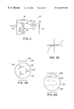
- FIG. 1 shows an exploded view of one embodiment of a printed flexible electrophoretic display.
- FIG. 2 shows a block diagram of an indicator prepared according to the present invention.
- FIG. 3 shows a circuit diagram of an embodiment of a battery indicator.
- FIG. 3A shows a voltage-current curve of a non-linear element included in a battery indicator.
- FIGS. 4A-4B show various embodiments of display media that is not bistable.
- FIGS. 5A-5F show various embodiments of a sticker display.
- FIG. 6A shows a flow chart illustrating how one embodiment of a radio-controlled display functions.
- FIG. 6B shows one embodiment of a radio-controlled display.
- FIG. 7 shows one embodiment of a radio paper.
- FIGS. 8A-8D depict a tile display system.
- FIG. 8E shows one embodiment of a block diagram of a tile display.
- FIG. 9 shows one embodiment of a wearable display.
- FIG. 10 shows a block diagram of one embodiment of network data displays.
- a substrate is provided and an electronic ink is printed onto a first area of the substrate.
- An electronic ink is an optoelectronically active material which comprises at least two phases: an electrophoretic contrast media phase and a coating/binding phase.
- the electrophoretic phase comprises, in some embodiments, a single species of electrophoretic particles dispersed in a clear or dyed medium, or more than one species of electrophoretic particles having distinct physical and electrical characteristics dispersed in a clear or dyed medium.
- the coating/binding phase includes, in one embodiment, a polymer matrix that surrounds the electrophoretic phase.
- the polymer in the polymeric binder is capable of being dried, crosslinked, or otherwise cured as in traditional inks, and therefore a printing process can be used to deposit the electronic ink onto a substrate.
- An electronic ink is capable of being printed by several different processes, depending on the mechanical properties of the specific ink employed. For example, the fragility or viscosity of a particular ink may result in a different process selection. A very viscous ink would not be well-suited to deposition by an inkjet printing process, while a fragile ink might not be used in a knife over roll coating process.
- the optical quality of an electronic ink is quite distinct from other electronic display materials.
- the most notable difference is that the electronic ink provides a high degree of both reflectance and contrast because it is pigment based (as are ordinary printing inks).
- the light scattered from the electronic ink comes from a very thin layer close to the top of the viewing surface. In this respect it resembles a common, printed image.
- electronic ink is easily viewed from a wide range of viewing angles in the same manner as a printed page.
- Such ink approximates a Lambertian contrast curve more closely than any other electronic display material.
- electronic ink can be printed, it can be included on the same surface with any other printed material.
- Electronic ink can be made optically stable in all optical states, that is, the ink can be set to a persistent optical state. Fabrication of a display by printing an electronic ink is particularly useful in low power applications because of this stability.
- the colors of electronically active and non-active inks may closely match and the reflectivities may be similar.
- Electronic inks can be printed so that no border is noticeable between active and non-active inks. This is referred to as “color matching” or “color masking”. Therefore, a display comprising an electronically active portion may appear as if it is not electronically active when the display is not being addressed and may be activated by addressing the display.
- Electronic inks are described in more detail in co-pending U.S. patent application Ser. No. 08/935,800, the contents of which are incorporated herein by reference.
- a display 1 is created by printing a first conductive coating 2 on a substrate 3 , printing an electronic ink 4 on the first conductive coating 2 , and printing a second conductive coating 6 on the electronic ink 4 .
- Conductive coatings 2 , 6 may be Indium Tin Oxide (ITO) or some other suitable conductive material.
- the conductive layers 2 , 6 may be applied from a vaporous phase, by electrolytic reaction, or deposition from a dispersed state such as spray droplets or dispersions in liquids. Conductive coatings 2 , 6 do not need to be the same conductive material.
- the substrate 3 is a polyester sheet having a thickness of about 4 mil
- the first conductive coating 2 is a transparent conductive coating such as ITO or a transparent polyaniline.
- the second conductive coating 6 may be an opaque conductive coating, such as a patterned graphite layer.
- the second conductive coating 6 can be polymeric.
- the polymer can be intrinsically conductive or can be a polymer carrier with a metal conductor such as a silver-doped polyester or a silver-doped vinyl resin.
- Conductive polymers suitable for use as the second electrode include, for example, polyaniline, polyprrole, polythiophene, polyphenylenevinylene, and their derivatives. These organic materials can be colloidally dispersed or dissolved in a suitable solvent before coating.
- a display 1 is created by printing a first conductive coating 2 , on a first substrate 3 (step 102 ) printing an electronic ink 4 on the first conductive coating 2 step ( 104 ) printing a second conductive coating 6 on a second substrate 3 ′ (step 106 ) and configuring the substrates 3 , 3 ′ such that the second conductive coating 6 is in electrical communication with the electronic ink 4 (step 108 ).
- the electronic ink 4 comprises a plurality of capsules.
- the capsules may have an average diameter on the order of about 100 microns. Capsules this small allow significant bending of the display substrate without permanent deformation or rupture of the capsules themselves. The optical appearance of the encapsulated medium itself is more or less unaffected by the curvature of these capsules.
- One of the benefits of using printing methods to fabricate displays is eliminating the need for vacuum-sputtered ITO by using coatable conductive materials.
- the replacement of vacuum-sputtered ITO with a printed conductive coating is beneficial in several ways.
- the printed conductor can be coated thinly, allowing for high optical transmission and low first-surface reflection. For example, total transmission can range from about 80% to about 95%.
- the printed conductive coating is significantly less expensive than vacuum-sputtered ITO.
- Another advantage of the encapsulated electrophoretic-display medium is that relatively poor conductors, for example, materials with resistivities on the order of 10 3 -10 12 ohms square, can be used as lead lines to address a display element.
- the flexible, inexpensive display described above is useful in numerous applications.
- these, flexible displays can be used in applications where paper is currently the display medium of choice.
- the displays can be made into disposable displays.
- the displays can be tightly rolled or bent double.
- the displays can be placed onto or incorporated into highly flexible plastic substrates, fabric, or paper. Since the displays can be rolled and bent without sustaining damage, they form large-area displays which are highly portable. Since these displays can be printed on plastics they can be lightweight.
- the printable, encapsulated electrophoretic display of the present invention can maintain the other desirable features of electrophoretic displays, including high reflectance, bistability, and low power consumption.
- FIG. 2 shows a block diagram of an indicator 10 .
- the indicator 10 includes an electronically addressable display 12 which is capable of changing between at least two states, and a transducer 14 which is capable of generating an electrical event to trigger the change in the state of the display 12 .
- the electronically addressable display 12 and the transducer 14 can both be printed onto a substrate 16 .
- FIG. 2 depicts an embodiment in which the indicator 10 further includes a printed battery 18 to power the transducer 14 and the display 12 .
- the transducer 14 need not be printed.
- a conventional transducer 14 may be placed on the substrate 16 .
- the display media 12 is printed as described above.
- the media 12 may be printed before or after the transducer adjacent which it is placed, provided that the display media 12 is ultimately in electrical communication with the transducer 14 .
- the battery 18 is a conventional battery, the voltage of which is measured and displayed on the display 12 .
- a battery indicator includes a printed display directly connected to a battery. The battery continuously addresses the display, but as the battery discharges over time, it eventually reaches a point where it is incapable of addressing the display. By varying the characteristics of the transducer, for example the number of amp-hours contained by the battery, the battery indicator can function as a “timer,” so that the display shows a message such as “expired” after passage of a certain electrical charge.
- FIG. 3 shows a circuit diagram of a battery indicator 20 .
- the battery indicator 20 includes a display 22 comprising a display media 24 , a first electrode 26 and a second electrode 27 disposed adjacent the display media 24 , a nonlinear element 28 in electrical communication with the first electrode 26 and a battery 30 , a voltage divider 32 in electrical communication with the battery 30 and the second electrode 27 , and a resistor 34 in communication with the nonlinear element 28 and the voltage divider 32 .
- the battery 30 can be of any type.
- the battery 30 initially has a maximum voltage.
- the voltage divider 32 establishes a voltage potential that is some fraction of the battery cell voltage at the second electrode 27 .
- the voltage divider 32 includes high impedance resistors 36 and 38 .
- the voltage divider 32 can have two 5 megaohm resistors to apply a voltage potential that is equal to one-half of the battery cell voltage to the second electrode 27 .
- the battery indicator can have a sliding voltage divider.
- a sliding voltage divider may be provided as a potentiometer using a non-linear element to control the voltage applied to the display 24 .
- the nonlinear element 28 conducts voltage equal to the battery cell voltage to the first electrode 26 when the battery cell voltage exceeds the predetermined threshold voltage.
- suitable non-linear elements include a transistor, Zener diode, varistor, metal-insulator-metal structure, organic semiconductors and devices based on materials like pentacene or regio-regular polythiophene, or any other nonlinear devices known to those skilled in the art.
- FIG. 3A shows an exemplary current-voltage characteristic of a nonlinear element 28 which can be used in the battery indicator 20 .
- the threshold voltage is adjustable through manufacturing, and the threshold is selected to be a voltage at which the battery 30 is still useable.
- a useful battery indicator should have a very low leakage current (e.g., much less than 1 microampere ( ⁇ A)) and should allow at least about a hundred times as much current to flow when it is on than when it is off.
- the threshold voltage at which the state of the display changes depends on the battery with which the indicator is designed to work.
- a threshold voltage of about 8 volts (V) is typical for a 9 V alkaline. For example at 9 V, the device should pass 1 ⁇ A, at 8 V the device should pass 100 nanoamperes (nA), and at 7 V the device should pass 10 nA.
- the voltage from the battery 30 which passes through the nonlinear element 28 and is applied to the first electrode 26 combined with the voltage from the battery 30 which passes through the voltage divider 32 and is applied to the second electrode 27 , to provide an electric field across the display media 24 sufficient to activate the display 22 .
- At least one of the first and second electrodes 26 , 27 comprises a clear conductive material to permit viewing of the display 22 .
- both electrodes may be placed on one side of the display media 24 , eliminating the need for a clear electrode.
- the resistor 34 can be a 10 megaohm resistor for a typical 9 V battery.
- the indicator 20 must draw less than 1 ⁇ (400 mAh/43800 h) in order for the battery 30 to have a suitable shelf life. Ideally, the indicator 20 should draw less than 1 ⁇ A. In order to achieve such a low current draw, the impedance of the indicator 20 must be in the order of 10 megaohms.
- Encapsulated electrophoretic display media includes a mixture of electrophoretic particles and a dye, or electrophoretic particles comprising multiple optical properties.
- the battery indicator 20 operates by applying an electric field of one polarity while the battery is good, and then switching to the opposite polarity when the battery goes bad.
- the display media is not required to be bistable.
- a display media 180 that is not bistable comprises at least one capsule 185 , each filled with electrophoretic particles 210 and a fluid 220 .
- Such media is useful in battery applications because the media will exhibit one contrast state when the display is addressed by the battery and a second contrast state when not addressed by the battery, i.e., when the battery voltage level falls below the threshold voltage necessary to address the display.
- electrophoretic particles 210 have polymer chain branches 200 which cause one particle 210 to repel another particle 210 .
- the fluid 220 is dyed to provide a color contrast with the particles 210 .
- This encapsulated display media 180 can be printed onto a substrate to form a display.
- an electrophoretic display that is not bistable can be formed by providing a standard display cell filled with electrophoretic media that is not bistable.
- another display media 290 that is also not bistable includes at least one microcapsule or cell 292 , filled with a plurality of metal sol 296 and a clear fluid 294 .
- Metal sol 296 comprises particles which are smaller than a wavelength of light.
- the metal sol 296 comprises gold sol.
- sol particles 296 agglomerate and scatter light.
- Brownian motion causes the sol particles 296 to redistribute, and the display media 290 appears clear from the clear fluid 294 .
- multiple indicators mapped to different voltage thresholds are used to create a battery indicator.
- An important element in this embodiment is a circuit element that provides a sharp non-linearity at a well-controlled voltage level.
- the battery indicator combines multiple non-linearities in order to provide a proper fit of the voltage curve for the open circuit voltage to be mapped to the closed circuit voltage. It is known that a battery with no load shows a voltage that is not the same as the loaded voltage. Therefore, non-linearity may be used to compensate for this difference. In addition, a known mapping of the closed circuit voltage to open circuit voltage may be used in the printed scale of the indicator.
- the invention features a timer.
- a timer includes ajunction formed of p-type semiconductor (e.g., boron doped) and an intrinsic or undoped semiconductor.
- p-type semiconductor e.g., boron doped
- an intrinsic or undoped semiconductor In this device, current does not flow. However, if the intrinsic semiconductor becomes n-doped (i.e., if the semiconductor has extra electrons available from the valence shell of dopant atoms), then current could flow from the n-doped region to the p-doped region. Normally, intrinsic semiconductors become n-doped if doped with phosphorous. Alternatively, the same result can be achieved by embedding or placing in close proximity to the intrinsic region a beta particle emitting substance such as tritium.
- an n-doped-intrinsic junction semiconductor may be treated with an alpha particle emitter such as Helium-5 to convert it to a p-doped region.
- an alpha particle emitter such as Helium-5 to convert it to a p-doped region.
- a non-conducting junction with an alpha or beta particle emitter embedded in its intrinsic region transforms into a diode-type junction which passes current, thereby acting as a timer.
- a timer employs a p-n junction semiconductor sensitive to light, such that light forces a current to flow from the n-region to the p-region.
- the timer can include a tritiated phosphor in a Zener diode and a display.
- a Zener diode is a diode designed to survive reverse breakdown. Light applied to the Zener diode through the tritiated phosphor increases the breakdown voltage of the Zener diode. When the tritiated system wears out, the Zener diode breakdown voltage decreases and voltage is applied to the display.
- a pressure indicator includes a transducer and a display.
- the transducer is printed.
- the display is an encapsulated electrophoretic display.
- the transducer for example, comprises a printed mechanical switch which closes once a certain pressure threshold is exceeded, thereby causing a printed display to change its state.
- pressure can change the electrical characteristics (e.g., the capacitance) of a circuit containing the display, thereby changing the state of the display once a threshold value has been exceeded.
- the transducer can provide power to switch the state of the display.
- a transducer is a piezoelectric element.
- a solar cell may provide power to the display.
- a heat indicator in another detailed embodiment, includes a display and a thermally-sensitive structure capable of changing the state of the display in response to a thermal stimulus.
- the structure is printed.
- the display is an encapsulated electrophoretic display.
- a printed bimetallic mechanical system can serve as an electrical switch which changes the state of the printed display.
- a printed chemical structure which reacts to a thermal condition can be used to change the resulting electrical properties and the state of the display.
- a transducer which provides power to switch the state of the display, for example, from an electrochemical potential.
- a solar cell may provide power to the display.
- a light indicator in another detailed embodiment, includes a display and a photosensitive structure capable of changing the state of the display in response to a photonic stimulus.
- the structure is printed.
- the display is an encapsulated electrophoretic display.
- a printed solar cell array has a photovoltaic characteristic which is capable of providing a voltage to switch the state of the display in response to incident photons.
- Other structures which are sensitive to other radiative ranges e.g. infrared, ultraviolet, etc.
- a solar cell may provide power to the display.
- a moisture indicator in another detailed embodiment, includes a display and a moisture-sensitive structure capable of changing the state of the display in response to humidity or direct aqueous contact.
- the structure is printed.
- the display is an encapsulated electrophoretic display.
- a structure can be printed which is an open circuit until an ionic solution bridges two exposed electrical contacts, thus changing the state of the display.
- a chemical structure can be printed which, after the absorption of a certain amount of water, changes the electrical properties sufficiently to change the state of the display. This transducer can provide power to switch the state of the display, for example using an accumulated electrochemical potential.
- Useful materials for this purpose include polyvinylalcohol, poly-N-vinylpyrrolidone, polyvinylpyrrolidone, derivatives of these materials, starches, and sugars.
- a solar cell may provide power to the display.
- a sound indicator includes a display and an acoustically-sensitive structure capable of changing the state of the display in response to an acoustical stimulus.
- the structure is printed.
- the display is an encapsulated electrophoretic display.
- a mechanically resonating structure could be printed which changes the state of the display based on piezoelectrically generated energy, similar to a microphone.
- a solar cell may provide power to the display.
- an angle indicator includes a display and a structure sensitive to orientation that is capable of changing the state of the display in response to a change in the orientation of the indicator.
- the structure is printed.
- the display is an encapsulated electrophoretic display.
- a mercury switch type structure could be provided which closes two electrical contacts when a certain orientation has been reached.
- the orientation structure can also provide power to switch the state of the display.
- the transducer can include a mechanical structure which converts a mechanical energy involved in angular rotation into an electrical energy.
- a solar cell may provide power to the display.
- a pH indicator in still another detailed embodiment, includes a display and a pH-sensitive structure capable of changing the state of the display in response to a change in the pH of a solution in which the indicator is immersed.
- the structure is printed.
- the display is an encapsulated electrophoretic display.
- a chemical cell which undergoes a chemical reaction at a certain pH level can be printed and can change the state of the display.
- the pH-sensitive structure can also provide power to switch the state of the display.
- an electrochemical potential can be generated by the chemical reaction.
- a solar cell may provide power to the display.
- a chemical indicator in still another detailed embodiment, includes a display and a chemically-sensitive structure capable of changing the state of the display in response to an external chemical interference.
- the structure is printed.
- the display is an encapsulated electrophoretic display.
- a printed chemical sensor can be sensitive to an externally introduced agent which causes a chemical reaction to occur, and switches the state of the display.
- the chemically-sensitive structure can also provide power to switch the state of the display.
- an electrochemical potential can be generated by the chemical reaction.
- a solar cell may provide power to the display.
- any of the above transducers can be connected to another transducer to create a multi-level transducer path which changes the state of display.
- an indicator can include a chemically-sensitive structure, a thermally-sensitive structure, and a display, all of which may be printed on a substrate. Heat from an exothermic reaction created by the chemically-sensitive structure can be sensed by the thermally-sensitive structure, which in turn changes the state of the display and may also be used to power the display.
- a printable, adhesive display 40 includes a substrate 42 coated with a conducting layer forming a top electrode 44 , a display media 46 disposed adjacent the top conductor 44 , and an adhesive 48 disposed adjacent the display media 40 .
- the display media 40 comprises an optoelectrically active component 50 and a binder 52 which holds the optoelectrically active component 50 together.
- the substrate 42 and the top electrode 44 are optically transmissive to allow the display 40 to be viewed through the electrode.
- the substrate 42 for example, can be formed of a polymeric material such as a polyester.
- the top electrode 44 can be formed of an inorganic material such as ITO or a suitable polymeric material.
- the optoelectronically active component 50 for example, can be an encapsulated electrophoretic display material. Alternatively, the optoelectronically active component 50 can be any other suitable display material such as bichronnal microspheres or liquid crystals.
- the binder 52 for example, can be selected from polyurethanes, polyvinylalcohols, gelatins, polyacrylates, polystyrenes, polyvinylbutyrals, polyesters, epoxies, silicones, polycarbonates, their derivatives, and pressure-sensitive urethanes and adhesives.
- the adhesive display 40 is attached to a receiving surface (not shown) by the adhesive 48 .
- the receiving surface may include rear electrodes for addressing the optoelectronically active component 50 .
- the rear electrodes may be electrically connected to drive or power circuitry for operating the display 40 .
- the display 40 is addressed in a “coupling” mode, where the top electrode 42 is “floating” and not directly tied to any specific potential.
- an adhesive display 56 includes a substrate 42 , a top electrode 44 disposed on the substrate 42 , a display media 46 comprising an optoelectronically active component 50 and a binder 52 , the display media 46 disposed adjacent the top electrode 44 , and an adhesive 48 disposed adjacent display the media 46 .
- the adhesive display 56 further includes a via 60 which electrically connects the top electrode 44 to a pad 62 disposed on a rear surface of the display media 46 , and a conductive adhesive 64 is disposed adjacent the pad 62 .
- the rear electrodes are disposed on a receiving surface (not shown) to which the adhesive display 56 is applied.
- the top electrode 44 may be directly connected to a specific potential.
- an adhesive display 70 includes a substrate 42 , a patterned, optically-transmissive conducting layer 72 forming a plurality of top electrodes, the layer 72 being on the substrate 42 , a display media 46 comprising an optoelectronically active component 50 and a binder 52 disposed adjacent the substrate 42 , and an adhesive 48 disposed adjacent the display media 46 .
- the adhesive display 70 further includes at least one via 60 which electrically connects at least one top electrode 72 to a pad 62 disposed on a rear surface of the display media 46 .
- a conductive adhesive 64 may be disposed adjacent the display media in the general location of the pads 62 .
- the rear electrodes may be disposed on a receiving surface (not shown) to which the adhesive display 70 is applied.
- an adhesive display 80 includes a substrate 42 , a continuous top electrode 44 disposed on the substrate 42 , a display media 46 comprising an optoelectronically active component 50 and a binder 52 disposed adjacent the top electrode 44 , at least one patterned rear electrode 82 disposed adjacent a rear surface of the display media 46 , and conductive adhesive 64 disposed adjacent the rear electrodes 82 for adhering the display 80 to a receiving surface (not shown).
- the receiving surface may include drive or power circuitry for operating the display 80 .
- the display 80 is addressed in a “coupling” mode where the top electrode is “floating.”
- an adhesive display 90 includes a substrate 42 , at least one patterned top electrode 72 disposed on the substrate 42 , a display media 46 comprising an optoelectronically active component 50 and a binder 52 disposed adjacent the top electrode 72 , at least one patterned rear electrode 82 disposed adjacent a rear surface of the display media 46 , and a dielectric layer 92 disposed adjacent the rear electrodes 82 .
- the adhesive display 90 further includes at least one via 60 which extends from a top electrode 72 through the display media 46 and the dielectric layer 92 to at least one pad 62 disposed on a rear surface of the dielectric layer 92 .
- the adhesive display 90 further includes at least one via 94 which extends from a rear electrode 82 through the dielectric layer 92 to at least one pad 96 disposed on a rear surface of the dielectric layer 92 .
- Conductive adhesive 64 is disposed in the general location of the pads 62 and 96 to adhere the display 90 to a receiving surface and to provide electrical communication between circuitry on the receiving surface and the electrodes 72 , 82 of the display 90 .
- the display 90 can further include a nonconductive adhesive 48 disposed adjacent the exposed dielectric layer 92 to fturther assist in adhering the display 90 to the receiver.
- an adhesive display 98 includes a substrate 42 , a display media 46 comprising an optoelectronically active component 50 and a binder 52 disposed adjacent the substrate 42 , and an adhesive 48 disposed adjacent a rear surface of the display media 46 .
- the display 98 is addressed by rear electrodes (not shown) only.
- the rear electrodes are disposed on a receiving surface to which the display 98 is applied.
- the rear electrodes may be disposed on a rear surface of the display 98 as shown in FIGS. 5D and 5E.
- a stylus may be provided that acts as the top electrode to address the adhesive display 40 .
- the stylus may be scanned over the entire display to address it.
- the stylus may be used as a writing utensil, addressing only specific portions of the display over which it is passed.
- an encapsulated, electrophoretic display is used to form a radio-controlled display system.
- the radio-controlled display system 300 includes a remote transmitter 370 , a receiver 301 , a controller 340 , and a display unit 350 .
- the receiver 301 includes an antenna 302 .
- the receiver 301 is in electrical communication with a passive rectifier 310 which transforms and rectifies energy received by the antenna 302 .
- the antenna 302 can be a monopole antenna, a dipole antenna, a planar array, a coil or any other antenna structure known in the art of radio reception.
- the antenna 302 may be disposed in a surrounding relation to the display 350 , allowing power to be received from relatively low-power signals.
- an antenna having a cross-sectional area of 0.1 square meters that receives a 10,000 watt signal at a distance of 5,000 m can receive 3 microwatts of power.
- the display 350 is powered by a solar cell (not shown).
- the antenna 302 includes a plurality of antennas to improve the reception level.
- the display system 300 further includes an energy storage device 320 in communication with the passive rectifier 310 .
- the energy storage device 320 can be a capacitor, a battery, or any other electrical or non-electrical energy storage device known in the art of energy storage. In the case of a non-electrical energy storage, a transducer can be used to transfer electrical energy into another form of energy.
- the controller 340 When the energy level in the energy storage device 320 reaches a certain level as detected by an energy level detector 330 , the controller 340 is activated and the display can be updated.
- the controller 340 decodes the radio signals received by the antenna 302 and updates the display 350 based on the information received by the antenna 302 .
- Each display 350 can have a unique identification code 360 that may be stored as dip switch settings or as programmed data in a semiconductor device such as a PROM or Flash RAM as in cellular phones or beepers.
- the controller 340 looks for this identification number 360 and updates the display 350 with the information on the attached data stream if a match between the transmitted ID code and the stored identification number 360 is made.
- the display 350 is a low power display.
- a bistable, non-emissive display such as an electrophoretic display can be used.
- an encapsulated, electrophoretic display which is inexpensive and easy to manufacture into a finished product, can be used.
- the radio-controlled display forms a radio sign that can be updated using information sent via radio-frequency energy.
- the sign includes a surface covered with a display material and control circuitry. This control circuitry receives broadcast energy. The circuitry decodes the information and updates the sign with that information.
- the display material for example, can be an encapsulated, electrophoretic display or any other encapsulated display material known to those skilled in the art. These display materials can be printed using traditional printing technology, thus facilitating and lowering the cost of sign manufacture.
- Radio signs can be used in stores, airports, train stations, on roads, supermarkets, at conventions, as billboards, or as any other signs where updating the signs or powering the signs may be best done remotely. Content may be updated using any form of electromagnetic radiation. These signs can use solar cells, batteries, or a hardwired source of power. These signs may be in two colors, three colors, four colors, or full color.
- a color display may be fabricated with a multi-step printing process.
- the first four steps can be a traditional four-color screen printing process to lay down an elaborate border or various static information that will not change throughout the lifetime of the device.
- the next step can be printing an electronic ink, which may be selected to match exactly the resultant colors from the four-color process.
- a top electrode is disposed on the printed electronic ink.
- the top electrode may also be printed using conventional printing techniques.
- the electronic ink comprises encapsulated electrophoretic ink which includes TiO 2 particles mixed into an organic fluid.
- the organic fluid for example, may contain a colored dye.
- the organic dispersion is emulsified into an aqueous solution and encapsulated using any of known encapsulation procedures known to those skilled in the art. Examples of such materials include gelatin-gum arabic or urea-formaldehyde microcapsules.
- the capsules are blended with a binding material to form a printable electronic ink suspension.
- a color display may be fabricated using a lamination process.
- static information is printed on a first substrate.
- the first embodiment includes at least one clear, or substantially clear, aperture.
- An encapsulated electrophoretic display is laminated to the printed substrate so that the display aligns with the aperture.
- a radio-controlled display forms a device capable of receiving broadcast data for individual consumption, referred to herein as a radio paper.
- the content may be customized for an individual, and a consumer of information could pay for such customized content using an electronic payment scheme.
- Radio paper may be two-color (e.g. black and white) or full color, as described above. Transactions for content may take place over one or more computer networks, including the world-wide computer network known as the Internet.
- a radio paper 400 includes a substrate 402 , a display 404 disposed on the substrate 402 , a receiver 406 disposed on the substrate 402 , and control circuitry 408 disposed on the substrate 402 .
- the display 404 can be printed onto the substrate 402 .
- the radio receiver 406 includes traces disposed on the substrate 402 .
- the radio receiver 406 includes an antenna mounted on the substrate 402 .
- the radio paper 400 can further include a power source 410 disposed on the substrate 402 .
- the power source 410 for example, can be a solar cell, a thin film battery, or a standard cell.
- the radio paper described above can be used to provide a wireless updatable document.
- the device includes: a document cover; an electronic display on any surface of the cover; and a data receiver.
- the display is fed by data from the data receiver.
- the display is visible to the document user and represents a way for the document to be messaged subsequent to its delivery.
- the device can be provided as a leaflet, book, magazine, circular, periodical, catalogue, directory or item containing a document cover.
- the electronic display of the device should operate using very low power and be easily visible.
- the general class of reflective electronic displays is desirable for this reason. Further ideally the display would be bistable, as described above, in order to minimize power draw.
- the display would be flexible and paper-thin to maximize the number of ways in which the display could be incorporated.
- a paper-thin substrate would allow the radio paper to be addressed by a desktop unit such as a laser printer.
- the radio paper could be addressed using a stylus that can be passed over the display.
- An encapsulated electrophoretic display meets all of the stated requirements, and may be used beneficially for this purpose.
- the data receiver may be any device capable of receiving information via electromagnetic radiation.
- the data receiver is a pager or other radio receiver.
- the data receiver may receive data via a physical connection, such as coaxial cable.
- the device may operate by battery power.
- the device may incorporate an appropriate sleep mechanism that causes the receiver to only be powered for reception during certain moments of the day when messages are expected to be sent, such as low traffic periods where bandwidth is cheaper.
- the device may also incorporate a solar cell to eliminate or reduce the need for batteries.
- an example of the usefulness of this device can be shown by reference to a chain of retail stores that distributes the device as a catalogue. After shipping the catalogue, the retailer may determine certain inventory items must be liquidated. This typically requires costly marketing efforts. Instead, using the device, the chain may advertise the items to be liquidated and may in fact refer the customer to specific pages of the catalogue. The chain may also promote events at the retail store and drive traffic to the store. The chain may also run various messages to different customer segments to evaluate offers and marketing messages on a trial basis.
- the device may be addressed either individually or as part of a group of devices. In the former case this permits targeted marketing and in the latter case this saves on bandwidth transmission costs.
- an encapsulated electrophoretic display is used to form a tile display, which allows creation of a large area display by interconnecting a plurality of tile displays.
- the tile displays when assembled, may or may not be seamless.
- Tile pixels may have any shape such as circular, rectangular or other shapes, for example, shapes present in a mosaic font display. There may be a pixel mask applied in front of the pixels.
- a tile display system 800 includes a plurality of tile displays 801 , 802 , 803 and 804 and a controller (not shown). Each tile display 801 includes means for connecting the tile display 801 to an adjacent tile display 802 , 803 , 804 .
- the tile display system 800 may include any desired number of tile displays. In one embodiment, the tile display system includes 40 ⁇ 30 grid of 16 ⁇ 16 pixel tiles to form a VGA resolution screen.
- the tile display system comprises a direct connect structure, that is, each pixel has its own lead line from the controller.
- Each lead line may be a discrete or packaged transistor line.
- a front surface of the substrate comprises of a grid of electrodes, where each electrode is connected through a via to the output of a control chip.
- N 2 +1 control lines are needed.
- the additional line is used to connect to a continuous top electrode.
- a matrix display using 2N+1 control lines can be built with a plurality of tile displays using a variety of techniques.
- an array of varistors, metal-insulator-metal, or discrete diodes are used for individually addressing each pixel.
- diodes discrete, surface-mount zener diodes are useful.
- the tiles are connected to each other using standard electronics connectors 805 placed on the edges of the tiles 801 as shown in FIGS. 8A-8D.
- the tiles are connected to each other using cables.
- the tiles can be mounted to a wall, lightweight metal grid, or any other substrate using nuts soldered onto the back of the tiles or by any other means known in the art of fastening substrates.
- the controller includes a microprocessor or other suitable drive circuitry.
- the controller transmits information to the tile displays to update the displays using any convenient form of electromagnetic radiation.
- the controller also receives information from the tile displays.
- Data for the display system may be stored in a memory element of the controller or may be received in the form of electromagnetic signals using a receiver.
- the receiver for example, can include an antenna and a passive rectifier in communication with the antenna, as described above.
- the controller connects to a single tile and controls the entire display.
- the controller can consist of a battery, a power supply, a paging receiver, and a microprocessor to control the entire system.
- the display can be powered, for example, using commercially available integrated AC to DC converters.
- each tile may have its own high voltage supply. Common inverter chips for use in electroluminescent backlights can be used in this embodiment.
- One method of controlling the entire tile system is to have a microcontroller on each tile.
- the sign controller tells the one tile it is connected to that it is at a certain coordinate location, say 0,0. Due to the asymmetrical connector layout, the tile can determine to which edge the controller is connected. That tile then communicates with its neighbors, incrementing or decrementing the coordinate location appropriately. Through this protocol, each tile can determine a unique identification code that specifies its location on the sign.
- the sign controller can then send data out on a common bus and each tile's microcontroller can receive data needed to update the tile. When the appropriate data appears on the bus, the microcontroller shifts this data out to the display drivers. Then, the entire sign is given a write pulse and the entire display is updated.
- the tile display as described above may be successfully driven with a voltage as low as 3 volts.
- the tile display is driven by controlling each pixel and the top electrode.
- the electrodes of the backplane are set to the proper pattern of voltages.
- the rear electrode segments are set at either ground or power and the top electrode is switched rapidly between ground and power.
- the top electrode is switched to ground, the other areas of the backplane that are at power will be switched. This method allows the backplane to maximize the voltage that the display material will receive.
- a standard bipolar addressing scheme may be used on the rear electrodes, with the top electrode held at ground potential.
- high voltage CMOS display drive circuitry such as HV57708PG manufactured by Supertex Corporation (Sunnyvale, Calif.) can be used to drive the tile display.
- the HV57708PG is an 80 pin plastic gull wing surface mount chip that has 64 outputs. Each output can sink 15 mA. Four of these chips can control a single tile.
- Other chips may find utility in the context of the present invention, such as the Sharp LH1538 which is an 80V 128 line Tape-Automated-Bonding (TAB) chip.
- TAB Tape-Automated-Bonding
- a tile display 830 includes a substrate 831 , and a display media 832 , electronics 834 , and driver circuitry 836 .
- the tile display 830 may be of any convenient size and may have any desired number of pixels. In one embodiment, the tile display 830 is 8 inches by 8 inches, and is a matrix of 16 ⁇ 16 pixels.
- the substrate 831 of the tile display 830 can be: a standard, etched printed circuit board; copper clad polyimide; polyester with printed conductive ink; or any other suitable substrate with patterned conductive areas.
- a display media 832 such as an encapsulated electrophoretic display media can be printed on a front surface of the substrate.
- the display media 832 can be an encapsulated electrophoretic suspension consisting of a slurry of capsules in a binder.
- Each capsule includes a mechanical system consisting of a dielectric suspending fluid and many particles. When an electric field is applied across the capsule, the particles are caused to move in the field. By using two different particle species of different charge and color such as black and white, the viewer can be presented with a color change.
- the material is bistable, so that once it is addressed, it stays in its last state. This is used to eliminate power draw between image updates. The material responds purely to the field, thus the only real current draw is in changing the charge of the plates on either side of the material.
- the capacitance of the display material can be between 0.1 and 100 picofarads per square centimeter. The capacitance will vary with differences in the display material, binder, and overall thickness.
- the display media is printed on a substrate and then covered with a layer of plastic or glass with a clear conductive coating such as ITO-coated, Mylar (Registered Trademark).
- a clear conductive coating such as ITO-coated, Mylar (Registered Trademark).
- Necessary connections to the ITO can be made using conductive adhesives, contacts, or tapes.
- the tile display 830 is prepared using the following steps.
- An electronic ink which forms the display media 832 is coated onto a conductive side of a sheet of ITO-sputtered Mylar 835 and then dried or cured.
- a layer of conductive adhesive 836 is optionally applied to the cured electronic ink 832 forming a laminate.
- This laminate is adhered to a backplane 837 made of a circuit board having copper pads 838 or screen-printed metallic inks disposed on its surface.
- the corners, or one edge 839 of the tile display 830 are reserved to allow connections to be made between the front ITO electrode 833 and the backplane 837 . If necessary, the electronic ink 832 is removed from the corners 839 and a connection is made using a conductive adhesive 836 such as silver loaded epoxy or a conductive heat seal.
- encapsulated electrophoretic displays are incorporated into clothing to provide a wearable display.
- a wearable display 502 is embodied as a patch on the arm 504 of a jacket 500 providing weather maps 506 or other information.
- the wearable display 502 includes a controller 508 in electrical communication with a display monitor 510 comprising an encapsulated, electrophoretic display media and a backplane.
- the display media is printed onto the backplane.
- the backplane further includes electronics necessary for addressing the display 502 .
- the wearable display is in communication with at least one device that provides data for display, such as a global positioning unit, news feed, or a pager. In these embodiments, the data device communicates information to the display which then displays the information for the wearer.
- Wearable displays can be incorporated into other wearable items such as shoes, socks, pants, underwear, wallets, key chains, shoe laces, suspenders, ties, bow ties, buttons, buckles, shirts, jackets, skirts, dresses, ear muffs, hats, glasses, contact lenses, watches, cuff links, wallet chains, belts, backpacks, briefcases, pocket books, gloves, raincoats, watchbands, bracelets, overcoats, windbreakers, vests, ponchos, waistcoats, or any other article of clothing or fashion accessory.
- wearable items such as shoes, socks, pants, underwear, wallets, key chains, shoe laces, suspenders, ties, bow ties, buttons, buckles, shirts, jackets, skirts, dresses, ear muffs, hats, glasses, contact lenses, watches, cuff links, wallet chains, belts, backpacks, briefcases, pocket books, gloves, raincoats, watchbands, bracelets, overcoats, windbreakers, vest
- the invention features a communications system.
- the communications system enables a whole new messaging and communication medium that permits its users to display messages in real time in practically any location.
- the system 1000 comprises a plurality of display receivers 1002 .
- the display receivers 1002 include an electronic display 1004 and a data receiver 1006 .
- the display receivers are tile displays or radio papers, as described above.
- the electronic display 1004 can operate by principles known to the art of LCDs, plasma displays, CRTs, electrophoretic displays or encapsulated electrophoretic displays.
- the encapsulated electrophoretic display may be coated onto many different surfaces practically any surface using appropriate binders such as PVCs, urethanes and silicon binders, allowing them to be: made in large sizes (such as poster and billboard sizes) using coating techniques; lightweight enough to install without an overhead crane; flexible enough to bend with wind; and capable of holding an image without further power draw, thereby operating economically from solar cells or batteries.
- appropriate binders such as PVCs, urethanes and silicon binders
- the data receiver 1006 may be, for example, a pager, cellular phone, satellite phone, radio-frequency receiver, infrared receiver, cable modem, or any other suitable receiver that is able to receive information from another source.
- the data receiver 1006 can transmit as well as receive information; for example the data receiver 1006 may transmit verification information to confirm that a new data stream was received.
- the data receiver 1006 may transmit data as may be useful for the overall operation of the system 1000 , for example weather data as part of a national weather system.
- the data receiver 1006 may use varying or multiple transmission methods for both receiving and transmitting data.
- the function of the data receiver 1006 is primarily to receive data and to display text or images in response.
- the data can include a message, a stream of messages, codes describing how the device should display or transition between the messages, or any other suitable information that will cause the display 1004 to operate as desired by the user.
- the data can also include a header, error-checking, checksum, routing or other information that facilitates the function of the system 1000 .
- the data receiver 1006 includes a control system 1008 .
- the control system 1008 facilitates the operation of the communications system 1000 .
- the control system 1008 functions as a user interface that permits the user to design, author, test, collaborate, approve and/or transmit images and commands that are sent to the display receivers.
- the control system 1008 functions as a billing and authorization system that monitors the user's activity, verifies payment has been received, verifies that the account is in good standing, verifies that the user has proper authorization, creates usage reports, generates invoices, and/or updates data receivers due to unsatisfactory billing status.
- control system 1008 functions as a data receiver management system that tracks data receivers, generates reports of data receiver history and status, permits sorting and screening of data receivers based on suitable characteristics, and/or permits the user to assign messages to the entire network of data receivers or subsets thereof.
- control system 1008 functions as a data transmission system that pre-processes data into a format suitable for the data receivers or subsets thereof, transmits the data by the method necessary or most suitable for each data receiver, schedules the transmission of the data according to desired criteria, verifies that the data was properly sent, receives and processes any information uploaded from the data receivers 1006 , resends messages that may not have been received, generates reports of such activities, and/or generates messages to field personnel indicating potential service requirements.
- control system may utilize the Internet or the World Wide Web as a user interface, as a data transmission mechanism, as an error-checking protocol, as a messaging service, as a programming environment or in any suitable fashion.
- the control system 1008 may also utilize data encryption mechanisms for enhanced security in the user interaction, in the system operation, in the data receiver transmission or in the data receiver reception.
- the control system 1008 may also utilize a suitable digital payment scheme to enable funds to be transferred as a part of the overall system of usage and operation.
Abstract
Description
Claims (14)
Priority Applications (1)
| Application Number | Priority Date | Filing Date | Title |
|---|---|---|---|
| US09/140,879 US6639578B1 (en) | 1995-07-20 | 1998-08-27 | Flexible displays |
Applications Claiming Priority (45)
| Application Number | Priority Date | Filing Date | Title |
|---|---|---|---|
| US08/504,896 US6124851A (en) | 1995-07-20 | 1995-07-20 | Electronic book with multiple page displays |
| US98340497A | 1997-07-19 | 1997-07-19 | |
| US5716397P | 1997-08-28 | 1997-08-28 | |
| US5711897P | 1997-08-28 | 1997-08-28 | |
| US5779997P | 1997-08-28 | 1997-08-28 | |
| US5779897P | 1997-08-28 | 1997-08-28 | |
| US5713397P | 1997-08-28 | 1997-08-28 | |
| US5771697P | 1997-08-28 | 1997-08-28 | |
| US5712297P | 1997-08-28 | 1997-08-28 | |
| US5954397P | 1997-09-19 | 1997-09-19 | |
| US5935897P | 1997-09-19 | 1997-09-19 | |
| US08/935,800 US6120588A (en) | 1996-07-19 | 1997-09-23 | Electronically addressable microencapsulated ink and display thereof |
| US6562997P | 1997-11-18 | 1997-11-18 | |
| US6563097P | 1997-11-18 | 1997-11-18 | |
| US6560597P | 1997-11-18 | 1997-11-18 | |
| US6614797P | 1997-11-19 | 1997-11-19 | |
| US6624697P | 1997-11-20 | 1997-11-20 | |
| US6624597P | 1997-11-20 | 1997-11-20 | |
| US6611597P | 1997-11-21 | 1997-11-21 | |
| US6633497P | 1997-11-21 | 1997-11-21 | |
| US6641897P | 1997-11-24 | 1997-11-24 | |
| US7093598P | 1998-01-09 | 1998-01-09 | |
| US7094098P | 1998-01-09 | 1998-01-09 | |
| US7093998P | 1998-01-09 | 1998-01-09 | |
| US7239098P | 1998-01-09 | 1998-01-09 | |
| US7137198P | 1998-01-15 | 1998-01-15 | |
| US7445498P | 1998-02-12 | 1998-02-12 | |
| US7695598P | 1998-03-05 | 1998-03-05 | |
| US7695998P | 1998-03-05 | 1998-03-05 | |
| US7695798P | 1998-03-05 | 1998-03-05 | |
| US7695698P | 1998-03-05 | 1998-03-05 | |
| US7697898P | 1998-03-05 | 1998-03-05 | |
| US7836398P | 1998-03-18 | 1998-03-18 | |
| US8136298P | 1998-04-10 | 1998-04-10 | |
| US8137498P | 1998-04-10 | 1998-04-10 | |
| US8325298P | 1998-04-27 | 1998-04-27 | |
| US8509698P | 1998-05-12 | 1998-05-12 | |
| US9022298P | 1998-06-22 | 1998-06-22 | |
| US9022398P | 1998-06-22 | 1998-06-22 | |
| US9023298P | 1998-06-22 | 1998-06-22 | |
| US9205098P | 1998-07-08 | 1998-07-08 | |
| US9204698P | 1998-07-08 | 1998-07-08 | |
| US9274298P | 1998-07-14 | 1998-07-14 | |
| US9368998P | 1998-07-22 | 1998-07-22 | |
| US09/140,879 US6639578B1 (en) | 1995-07-20 | 1998-08-27 | Flexible displays |
Related Parent Applications (1)
| Application Number | Title | Priority Date | Filing Date |
|---|---|---|---|
| US08/935,800 Continuation-In-Part US6120588A (en) | 1995-07-20 | 1997-09-23 | Electronically addressable microencapsulated ink and display thereof |
Publications (1)
| Publication Number | Publication Date |
|---|---|
| US6639578B1 true US6639578B1 (en) | 2003-10-28 |
Family
ID=29274019
Family Applications (1)
| Application Number | Title | Priority Date | Filing Date |
|---|---|---|---|
| US09/140,879 Expired - Fee Related US6639578B1 (en) | 1995-07-20 | 1998-08-27 | Flexible displays |
Country Status (1)
| Country | Link |
|---|---|
| US (1) | US6639578B1 (en) |
Cited By (330)
| Publication number | Priority date | Publication date | Assignee | Title |
|---|---|---|---|---|
| US20010052840A1 (en) * | 2000-06-20 | 2001-12-20 | Ranjan Ghosh | Paging device |
| US20020030638A1 (en) * | 2000-05-19 | 2002-03-14 | Michael Weiner | Apparatus for the display of embedded information |
| US20020131147A1 (en) * | 1998-08-27 | 2002-09-19 | Paolini Richard J. | Electrophoretic medium and process for the production thereof |
| US20020167500A1 (en) * | 1998-09-11 | 2002-11-14 | Visible Techknowledgy, Llc | Smart electronic label employing electronic ink |
| US20020196526A1 (en) * | 2001-03-30 | 2002-12-26 | Hideyuki Kawai | Electrophoretic device, method for driving the same, and electronic apparatus |
| US20030016590A1 (en) * | 2001-07-19 | 2003-01-23 | Brewer Donald R. | Timepiece module with bi-stable display |
| US20030197915A1 (en) * | 2002-04-23 | 2003-10-23 | Jack Hou | Segment electrophoretic displays and methods for their manufacture |
| US20030222315A1 (en) * | 2002-04-24 | 2003-12-04 | E Ink Corporation | Backplanes for display applications, and components for use therein |
| US20040119602A1 (en) * | 1999-05-04 | 2004-06-24 | Blum Ronald D. | Floor display system with variable image orientation |
| US20040217877A1 (en) * | 1999-05-04 | 2004-11-04 | William Kokonaski | Flexible electronic display and wireless communication system |
| US20040233509A1 (en) * | 2002-12-23 | 2004-11-25 | E Ink Corporation | Flexible electro-optic displays |
| US20050082820A1 (en) * | 2002-10-09 | 2005-04-21 | Nelson Veronica A. | Flexible sheet having at least one region of electroluminescence |
| WO2005054933A2 (en) | 2003-11-26 | 2005-06-16 | E Ink Corporation | Electro-optic displays with reduced remnant voltage |
| US20050174340A1 (en) * | 2002-05-29 | 2005-08-11 | Zbd Displays Limited | Display device having a material with at least two stable configurations |
| US20050181275A1 (en) * | 2004-02-18 | 2005-08-18 | Jang Bor Z. | Open electrochemical cell, battery and functional device |
| US20050205402A1 (en) * | 2004-03-17 | 2005-09-22 | Wright James B | Illuminated vehicle remote entry device |
| US6950220B2 (en) | 2002-03-18 | 2005-09-27 | E Ink Corporation | Electro-optic displays, and methods for driving same |
| US6958848B2 (en) | 2002-05-23 | 2005-10-25 | E Ink Corporation | Capsules, materials for use therein and electrophoretic media and displays containing such capsules |
| US20050272408A1 (en) * | 2004-06-04 | 2005-12-08 | Deanna Wilkes-Gibbs | Method for personal notification indication |
| US6982178B2 (en) | 2002-06-10 | 2006-01-03 | E Ink Corporation | Components and methods for use in electro-optic displays |
| US6987603B2 (en) | 2003-01-31 | 2006-01-17 | E Ink Corporation | Construction of electrophoretic displays |
| US20060044149A1 (en) * | 1999-05-04 | 2006-03-02 | Blum Ronald D | Electronic floor display with alerting |
| US7012735B2 (en) | 2003-03-27 | 2006-03-14 | E Ink Corporaiton | Electro-optic assemblies, and materials for use therein |
| US7030854B2 (en) | 2001-03-13 | 2006-04-18 | E Ink Corporation | Apparatus for displaying drawings |
| US20060138948A1 (en) * | 2004-12-27 | 2006-06-29 | Quantum Paper, Inc. | Addressable and printable emissive display |
| US20060138944A1 (en) * | 2004-12-27 | 2006-06-29 | Quantum Paper | Addressable and printable emissive display |
| US7075703B2 (en) | 2004-01-16 | 2006-07-11 | E Ink Corporation | Process for sealing electro-optic displays |
| US7079305B2 (en) | 2001-03-19 | 2006-07-18 | E Ink Corporation | Electrophoretic medium and process for the production thereof |
| US20060171104A1 (en) * | 2005-02-01 | 2006-08-03 | Sap Aktiengesellschaft | Portable device with programmable housing |
| US20060187267A1 (en) * | 2005-02-18 | 2006-08-24 | Lexmark International, Inc. | Printed conductive connectors |
| US20060192683A1 (en) * | 1999-05-04 | 2006-08-31 | Blum Ronald D | Modular protective structure for floor display |
| US7116466B2 (en) | 2004-07-27 | 2006-10-03 | E Ink Corporation | Electro-optic displays |
| US20060223282A1 (en) * | 2002-04-24 | 2006-10-05 | E Ink Corporation | Processes for forming backplanes for electro-optic displays |
| US20060256424A1 (en) * | 2000-03-03 | 2006-11-16 | Jack Hou | Segment electrophoretic displays and methods for their manufacture |
| US7173752B2 (en) | 2003-11-05 | 2007-02-06 | E Ink Corporation | Electro-optic displays, and materials for use therein |
| US20070029939A1 (en) * | 2005-08-05 | 2007-02-08 | Philip Burkum | Electroluminescent sign having a coded information region |
| US20070040489A1 (en) * | 2004-12-27 | 2007-02-22 | Quantum Paper, Inc. | Static and addressable emissive displays |
| US7190008B2 (en) | 2002-04-24 | 2007-03-13 | E Ink Corporation | Electro-optic displays, and components for use therein |
| US20070067726A1 (en) * | 2005-09-16 | 2007-03-22 | Microsoft Corporation | Content sharing user interface for mobile devices |
| US20070067272A1 (en) * | 2005-09-16 | 2007-03-22 | Microsoft Corporation | Search interface for mobile devices |
| US20070082707A1 (en) * | 2005-09-16 | 2007-04-12 | Microsoft Corporation | Tile space user interface for mobile devices |
| US7206119B2 (en) | 2003-12-31 | 2007-04-17 | E Ink Corporation | Electro-optic displays, and method for driving same |
| US7230751B2 (en) | 2005-01-26 | 2007-06-12 | E Ink Corporation | Electrophoretic displays using gaseous fluids |
| US20070168414A1 (en) * | 2006-01-13 | 2007-07-19 | Arnold Brent D | Managing advertising devices |
| US7259744B2 (en) | 1995-07-20 | 2007-08-21 | E Ink Corporation | Dielectrophoretic displays |
| WO2007104003A2 (en) | 2006-03-08 | 2007-09-13 | E Ink Corporation | Methods for production of electro-optic displays |
| US20070237906A1 (en) * | 2004-01-28 | 2007-10-11 | Kent Displays Incorporated | Chiral nematic photo displays |
| US20070279400A1 (en) * | 2006-06-05 | 2007-12-06 | Ryuichi Iwamura | Electronic device with a thin display |
| US7339715B2 (en) | 2003-03-25 | 2008-03-04 | E Ink Corporation | Processes for the production of electrophoretic displays |
| US20080055105A1 (en) * | 1999-05-04 | 2008-03-06 | Intellimat, Inc. | Floor display system with interactive features and variable image rotation |
| US7365733B2 (en) | 2002-12-16 | 2008-04-29 | E Ink Corporation | Backplanes for electro-optic displays |
| US20080117495A1 (en) * | 1995-07-20 | 2008-05-22 | E Ink Corporation | Dielectrophoretic displays |
| US7420549B2 (en) | 2003-10-08 | 2008-09-02 | E Ink Corporation | Electro-wetting displays |
| US20080211765A1 (en) * | 1995-07-20 | 2008-09-04 | E Ink Corporation | Stylus-based addressing structures for displays |
| US20080217412A1 (en) * | 2007-02-22 | 2008-09-11 | Karen Nixon Lane | Segmented microencapsulated display system |
| US20080217414A1 (en) * | 2007-03-09 | 2008-09-11 | Oki Data Corporation | Flexible display member and article having the same |
| US20080297453A1 (en) * | 2007-05-31 | 2008-12-04 | Applied Printed Electronics Holdings, Inc. | Method of Manufacturing Addressable and Static Electronic Displays |
| US20080303436A1 (en) * | 2003-08-30 | 2008-12-11 | Charles Forbes | Method for pattern metalization of substrates |
| US20080309598A1 (en) * | 2004-01-28 | 2008-12-18 | Doane J William | Stacked color photodisplay |
| US7477444B2 (en) | 2006-09-22 | 2009-01-13 | E Ink Corporation & Air Products And Chemical, Inc. | Electro-optic display and materials for use therein |
| US20090014532A1 (en) * | 1998-09-11 | 2009-01-15 | Metrologic Instruments, Inc. | Electronic-ink based display system employing a plurality of RF-based activator modules in wireless communication with a plurality of remotely-updateable electronic display devices, each employing an electronic ink layer integrated within a stacked architecture |
| US20090027762A1 (en) * | 1995-07-20 | 2009-01-29 | E Ink Corporation | Electro-osmotic displays and materials for making the same |
| US20090033811A1 (en) * | 2007-07-31 | 2009-02-05 | Kent Displays Incorporated | Multiple color writing tablet |
| US20090096942A1 (en) * | 2007-07-31 | 2009-04-16 | Kent Displays Incorporated | Selectively erasable electronic writing tablet |
| US20090140875A1 (en) * | 2005-05-26 | 2009-06-04 | Hendrik Sjirk Wagter | Portable optical signalling device |
| US20090157354A1 (en) * | 2007-12-12 | 2009-06-18 | Motorola, Inc. | Labeling methods and devices |
| US7551346B2 (en) | 2003-11-05 | 2009-06-23 | E Ink Corporation | Electro-optic displays, and materials for use therein |
| US7554712B2 (en) | 2005-06-23 | 2009-06-30 | E Ink Corporation | Edge seals for, and processes for assembly of, electro-optic displays |
| US7602374B2 (en) | 2003-09-19 | 2009-10-13 | E Ink Corporation | Methods for reducing edge effects in electro-optic displays |
| US20090284179A1 (en) * | 2008-05-13 | 2009-11-19 | Nthdegree Technologies Worldwide Inc. | Apparatuses for Providing Power for Illumination of a Display Object |
| US20090284164A1 (en) * | 2008-05-13 | 2009-11-19 | Nthdegree Technologies Worldwide Inc. | Illuminating Display Systems |
| US20100011291A1 (en) * | 2008-07-10 | 2010-01-14 | Nokia Corporation | User interface, device and method for a physically flexible device |
| US7649674B2 (en) | 2002-06-10 | 2010-01-19 | E Ink Corporation | Electro-optic display with edge seal |
| US7649666B2 (en) | 2006-12-07 | 2010-01-19 | E Ink Corporation | Components and methods for use in electro-optic displays |
| US20100040844A1 (en) * | 2007-04-25 | 2010-02-18 | Tesserae Technologies | System and method for color-changing decorative construction materials |
| US7667886B2 (en) | 2007-01-22 | 2010-02-23 | E Ink Corporation | Multi-layer sheet for use in electro-optic displays |
| US20100045180A1 (en) * | 2008-08-19 | 2010-02-25 | World Properties, Inc. | Liquid crystal display with split electrode |
| US7672040B2 (en) | 2003-11-05 | 2010-03-02 | E Ink Corporation | Electro-optic displays, and materials for use therein |
| US7679814B2 (en) | 2001-04-02 | 2010-03-16 | E Ink Corporation | Materials for use in electrophoretic displays |
| US20100068838A1 (en) * | 2007-05-31 | 2010-03-18 | Nthdegree Technologies Worldwide Inc. | Method of Manufacturing a Light Emitting, Photovoltaic or Other Electronic Apparatus and System |
| US20100066484A1 (en) * | 2008-09-15 | 2010-03-18 | Commtiva Technology Corporation | Remote monitor/control for billboard lighting or standby power system |
| US7688297B2 (en) | 1999-04-30 | 2010-03-30 | E Ink Corporation | Methods for driving bistable electro-optic displays, and apparatus for use therein |
| US7688497B2 (en) | 2007-01-22 | 2010-03-30 | E Ink Corporation | Multi-layer sheet for use in electro-optic displays |
| US7733311B2 (en) | 1999-04-30 | 2010-06-08 | E Ink Corporation | Methods for driving bistable electro-optic displays, and apparatus for use therein |
| US20100141692A1 (en) * | 2007-05-28 | 2010-06-10 | Tyson York Winarski | Multicolor visual feedback for non-volatile storage |
| US7773064B2 (en) | 2003-07-02 | 2010-08-10 | Kent Displays Incorporated | Liquid crystal display films |
| US7791782B2 (en) | 2002-06-10 | 2010-09-07 | E Ink Corporation | Electro-optics displays, and processes for the production thereof |
| US7791489B2 (en) | 2003-09-03 | 2010-09-07 | Metrologic Instruments, Inc. | Electronic-ink based RFID tag for attachment to a consumer item and displaying graphical indicia indicating whether or not said consumer items has been read and its integrated RFID module has been activated or deactivated |
| US7796103B2 (en) | 2004-01-28 | 2010-09-14 | Kent Displays Incorporated | Drapable liquid crystal transfer display films |
| US20100245112A1 (en) * | 2007-09-12 | 2010-09-30 | Polyic Gmbh & Co. Kg | Multilayer flexible film body |
| US20100265214A1 (en) * | 2007-07-31 | 2010-10-21 | Kent Displays Incorporated | Writing tablet information recording device |
| US7826129B2 (en) | 2007-03-06 | 2010-11-02 | E Ink Corporation | Materials for use in electrophoretic displays |
| US20100277441A1 (en) * | 2007-10-06 | 2010-11-04 | Polyic Gmbh & Co. Kg | Security element for the identification of a security document and method for producing it |
| US20100283806A1 (en) * | 1997-08-28 | 2010-11-11 | E Ink Corporation | Multi-color electrophoretic displays and materials for making the same |
| US7839564B2 (en) | 2002-09-03 | 2010-11-23 | E Ink Corporation | Components and methods for use in electro-optic displays |
| US7843626B2 (en) | 2001-07-09 | 2010-11-30 | E Ink Corporation | Electro-optic display and materials for use therein |
| US7843621B2 (en) | 2002-06-10 | 2010-11-30 | E Ink Corporation | Components and testing methods for use in the production of electro-optic displays |
| US7843624B2 (en) | 2006-03-08 | 2010-11-30 | E Ink Corporation | Electro-optic displays, and materials and methods for production thereof |
| US7848006B2 (en) | 1995-07-20 | 2010-12-07 | E Ink Corporation | Electrophoretic displays with controlled amounts of pigment |
| US7848007B2 (en) | 1995-07-20 | 2010-12-07 | E Ink Corporation | Electrophoretic medium and process for the production thereof |
| US7859637B2 (en) | 1999-07-21 | 2010-12-28 | E Ink Corporation | Use of a storage capacitor to enhance the performance of an active matrix driven electronic display |
| US20110005325A1 (en) * | 2009-07-13 | 2011-01-13 | National Taiwan University | Design and fabrication method of a flexible capacitive pressure sensor |
| WO2011005318A2 (en) | 2009-07-10 | 2011-01-13 | Roel Vertegaal | Interaction techniques for flexible displays |
| US7893435B2 (en) | 2000-04-18 | 2011-02-22 | E Ink Corporation | Flexible electronic circuits and displays including a backplane comprising a patterned metal foil having a plurality of apertures extending therethrough |
| US20110043726A1 (en) * | 2009-08-18 | 2011-02-24 | World Properties, Inc. | Display with split electrode between two substrates |
| US7903319B2 (en) | 2006-07-11 | 2011-03-08 | E Ink Corporation | Electrophoretic medium and display with improved image stability |
| US20110056564A1 (en) * | 2008-05-09 | 2011-03-10 | Korgel Brian A | Nanoparticles and methods of making and using |
| US7910175B2 (en) | 2003-03-25 | 2011-03-22 | E Ink Corporation | Processes for the production of electrophoretic displays |
| US7952557B2 (en) | 2001-11-20 | 2011-05-31 | E Ink Corporation | Methods and apparatus for driving electro-optic displays |
| US7952790B2 (en) | 2006-03-22 | 2011-05-31 | E Ink Corporation | Electro-optic media produced using ink jet printing |
| US7956841B2 (en) | 1995-07-20 | 2011-06-07 | E Ink Corporation | Stylus-based addressing structures for displays |
| US7957053B2 (en) | 2003-07-24 | 2011-06-07 | E Ink Corporation | Electro-optic displays |
| US7959769B2 (en) | 2004-12-08 | 2011-06-14 | Infinite Power Solutions, Inc. | Deposition of LiCoO2 |
| US7972875B2 (en) | 2007-01-17 | 2011-07-05 | The Board Of Trustees Of The University Of Illinois | Optical systems fabricated by printing-based assembly |
| US7982296B2 (en) | 2004-06-04 | 2011-07-19 | The Board Of Trustees Of The University Of Illinois | Methods and devices for fabricating and assembling printable semiconductor elements |
| US7986450B2 (en) | 2006-09-22 | 2011-07-26 | E Ink Corporation | Electro-optic display and materials for use therein |
| US7993773B2 (en) | 2002-08-09 | 2011-08-09 | Infinite Power Solutions, Inc. | Electrochemical apparatus with barrier layer protected substrate |
| US7999787B2 (en) | 1995-07-20 | 2011-08-16 | E Ink Corporation | Methods for driving electrophoretic displays using dielectrophoretic forces |
| US8009348B2 (en) | 1999-05-03 | 2011-08-30 | E Ink Corporation | Machine-readable displays |
| US8018640B2 (en) | 2006-07-13 | 2011-09-13 | E Ink Corporation | Particles for use in electrophoretic displays |
| US8021778B2 (en) | 2002-08-09 | 2011-09-20 | Infinite Power Solutions, Inc. | Electrochemical apparatus with barrier layer protected substrate |
| US8034209B2 (en) | 2007-06-29 | 2011-10-11 | E Ink Corporation | Electro-optic displays, and materials and methods for production thereof |
| US8039847B2 (en) | 2004-06-04 | 2011-10-18 | The Board Of Trustees Of The University Of Illinois | Printable semiconductor structures and related methods of making and assembling |
| US8040594B2 (en) | 1997-08-28 | 2011-10-18 | E Ink Corporation | Multi-color electrophoretic displays |
| US8049947B2 (en) | 2002-06-10 | 2011-11-01 | E Ink Corporation | Components and methods for use in electro-optic displays |
| US8054526B2 (en) | 2008-03-21 | 2011-11-08 | E Ink Corporation | Electro-optic displays, and color filters for use therein |
| US8062708B2 (en) | 2006-09-29 | 2011-11-22 | Infinite Power Solutions, Inc. | Masking of and material constraint for depositing battery layers on flexible substrates |
| US8098418B2 (en) | 2009-03-03 | 2012-01-17 | E. Ink Corporation | Electro-optic displays, and color filters for use therein |
| US8097926B2 (en) | 2008-10-07 | 2012-01-17 | Mc10, Inc. | Systems, methods, and devices having stretchable integrated circuitry for sensing and delivering therapy |
| US8115729B2 (en) | 1999-05-03 | 2012-02-14 | E Ink Corporation | Electrophoretic display element with filler particles |
| US8125501B2 (en) | 2001-11-20 | 2012-02-28 | E Ink Corporation | Voltage modulated driver circuits for electro-optic displays |
| US8129655B2 (en) | 2002-09-03 | 2012-03-06 | E Ink Corporation | Electrophoretic medium with gaseous suspending fluid |
| US8139050B2 (en) | 1995-07-20 | 2012-03-20 | E Ink Corporation | Addressing schemes for electronic displays |
| US8174490B2 (en) | 2003-06-30 | 2012-05-08 | E Ink Corporation | Methods for driving electrophoretic displays |
| US8177942B2 (en) | 2003-11-05 | 2012-05-15 | E Ink Corporation | Electro-optic displays, and materials for use therein |
| US8197781B2 (en) | 2006-11-07 | 2012-06-12 | Infinite Power Solutions, Inc. | Sputtering target of Li3PO4 and method for producing same |
| US8198621B2 (en) | 2004-06-04 | 2012-06-12 | The Board Of Trustees Of The University Of Illinois | Stretchable form of single crystal silicon for high performance electronics on rubber substrates |
| US8234507B2 (en) | 2009-01-13 | 2012-07-31 | Metrologic Instruments, Inc. | Electronic-ink display device employing a power switching mechanism automatically responsive to predefined states of device configuration |
| US8236443B2 (en) | 2002-08-09 | 2012-08-07 | Infinite Power Solutions, Inc. | Metal film encapsulation |
| US8260203B2 (en) | 2008-09-12 | 2012-09-04 | Infinite Power Solutions, Inc. | Energy device with integral conductive surface for data communication via electromagnetic energy and method thereof |
| US8268488B2 (en) | 2007-12-21 | 2012-09-18 | Infinite Power Solutions, Inc. | Thin film electrolyte for thin film batteries |
| US8270064B2 (en) | 2009-02-09 | 2012-09-18 | E Ink Corporation | Electrophoretic particles, and processes for the production thereof |
| US8289250B2 (en) | 2004-03-31 | 2012-10-16 | E Ink Corporation | Methods for driving electro-optic displays |
| US8314784B2 (en) | 2008-04-11 | 2012-11-20 | E Ink Corporation | Methods for driving electro-optic displays |
| US8319759B2 (en) | 2003-10-08 | 2012-11-27 | E Ink Corporation | Electrowetting displays |
| US8350519B2 (en) | 2008-04-02 | 2013-01-08 | Infinite Power Solutions, Inc | Passive over/under voltage control and protection for energy storage devices associated with energy harvesting |
| US8363299B2 (en) | 2002-06-10 | 2013-01-29 | E Ink Corporation | Electro-optic displays, and processes for the production thereof |
| EP2555182A1 (en) | 2007-02-02 | 2013-02-06 | E Ink Corporation | Electrophoretic displays having transparent electrode and conductor connected thereto |
| US8372726B2 (en) | 2008-10-07 | 2013-02-12 | Mc10, Inc. | Methods and applications of non-planar imaging arrays |
| US8390301B2 (en) | 2006-03-08 | 2013-03-05 | E Ink Corporation | Electro-optic displays, and materials and methods for production thereof |
| US8389862B2 (en) | 2008-10-07 | 2013-03-05 | Mc10, Inc. | Extremely stretchable electronics |
| US8390918B2 (en) | 2001-04-02 | 2013-03-05 | E Ink Corporation | Electrophoretic displays with controlled amounts of pigment |
| US8394522B2 (en) | 2002-08-09 | 2013-03-12 | Infinite Power Solutions, Inc. | Robust metal film encapsulation |
| US8404376B2 (en) | 2002-08-09 | 2013-03-26 | Infinite Power Solutions, Inc. | Metal film encapsulation |
| US20130076711A1 (en) * | 2006-03-31 | 2013-03-28 | Ryutaro Sakai | E-ink touchscreen visualizer for home av system |
| US8415879B2 (en) | 2007-05-31 | 2013-04-09 | Nthdegree Technologies Worldwide Inc | Diode for a printable composition |
| US8431264B2 (en) | 2002-08-09 | 2013-04-30 | Infinite Power Solutions, Inc. | Hybrid thin-film battery |
| EP2590011A2 (en) * | 2010-06-29 | 2013-05-08 | Nanobrick Co., Ltd. | Method for displaying surface and apparatus thereof |
| US8445130B2 (en) | 2002-08-09 | 2013-05-21 | Infinite Power Solutions, Inc. | Hybrid thin-film battery |
| US8446664B2 (en) | 2010-04-02 | 2013-05-21 | E Ink Corporation | Electrophoretic media, and materials for use therein |
| WO2013074167A1 (en) | 2011-11-18 | 2013-05-23 | Avon Products, Inc. | Use of electrophoretic microcapsules in a cosmetic composition |
| US8457013B2 (en) | 2009-01-13 | 2013-06-04 | Metrologic Instruments, Inc. | Wireless dual-function network device dynamically switching and reconfiguring from a wireless network router state of operation into a wireless network coordinator state of operation in a wireless communication network |
| US8470701B2 (en) | 2008-04-03 | 2013-06-25 | Advanced Diamond Technologies, Inc. | Printable, flexible and stretchable diamond for thermal management |
| US8508193B2 (en) | 2008-10-08 | 2013-08-13 | Infinite Power Solutions, Inc. | Environmentally-powered wireless sensor module |
| US8518581B2 (en) | 2008-01-11 | 2013-08-27 | Inifinite Power Solutions, Inc. | Thin film encapsulation for thin film batteries and other devices |
| US8525346B2 (en) | 2009-06-02 | 2013-09-03 | Hsio Technologies, Llc | Compliant conductive nano-particle electrical interconnect |
| US8552299B2 (en) | 2008-03-05 | 2013-10-08 | The Board Of Trustees Of The University Of Illinois | Stretchable and foldable electronic devices |
| US8558783B2 (en) | 2001-11-20 | 2013-10-15 | E Ink Corporation | Electro-optic displays with reduced remnant voltage |
| US8593396B2 (en) | 2001-11-20 | 2013-11-26 | E Ink Corporation | Methods and apparatus for driving electro-optic displays |
| US8599572B2 (en) | 2009-09-01 | 2013-12-03 | Infinite Power Solutions, Inc. | Printed circuit board with integrated thin film battery |
| US8610988B2 (en) | 2006-03-09 | 2013-12-17 | E Ink Corporation | Electro-optic display with edge seal |
| US8610265B2 (en) | 2009-06-02 | 2013-12-17 | Hsio Technologies, Llc | Compliant core peripheral lead semiconductor test socket |
| US8618649B2 (en) | 2009-06-02 | 2013-12-31 | Hsio Technologies, Llc | Compliant printed circuit semiconductor package |
| US8636876B2 (en) | 2004-12-08 | 2014-01-28 | R. Ernest Demaray | Deposition of LiCoO2 |
| US8654436B1 (en) | 2009-10-30 | 2014-02-18 | E Ink Corporation | Particles for use in electrophoretic displays |
| EP2698784A1 (en) | 2003-08-19 | 2014-02-19 | E Ink Corporation | Methods for controlling electro-optic displays |
| US8666471B2 (en) | 2010-03-17 | 2014-03-04 | The Board Of Trustees Of The University Of Illinois | Implantable biomedical devices on bioresorbable substrates |
| US8674593B2 (en) | 2007-05-31 | 2014-03-18 | Nthdegree Technologies Worldwide Inc | Diode for a printable composition |
| EP2711770A2 (en) | 2005-10-18 | 2014-03-26 | E Ink Corporation | Components for electro-optic displays |
| US8728285B2 (en) | 2003-05-23 | 2014-05-20 | Demaray, Llc | Transparent conductive oxides |
| US8754859B2 (en) | 2009-10-28 | 2014-06-17 | E Ink Corporation | Electro-optic displays with touch sensors and/or tactile feedback |
| US8758067B2 (en) | 2010-06-03 | 2014-06-24 | Hsio Technologies, Llc | Selective metalization of electrical connector or socket housing |
| US8789272B2 (en) | 2009-06-02 | 2014-07-29 | Hsio Technologies, Llc | Method of making a compliant printed circuit peripheral lead semiconductor test socket |
| US8801497B2 (en) | 2009-04-30 | 2014-08-12 | Rdc Holdings, Llc | Array of abrasive members with resilient support |
| US8803539B2 (en) | 2009-06-03 | 2014-08-12 | Hsio Technologies, Llc | Compliant wafer level probe assembly |
| US8809126B2 (en) | 2007-05-31 | 2014-08-19 | Nthdegree Technologies Worldwide Inc | Printable composition of a liquid or gel suspension of diodes |
| WO2014135847A2 (en) * | 2013-03-07 | 2014-09-12 | Plastic Logic Limited | Tiled displays |
| US8846457B2 (en) | 2007-05-31 | 2014-09-30 | Nthdegree Technologies Worldwide Inc | Printable composition of a liquid or gel suspension of diodes |
| US8852467B2 (en) | 2007-05-31 | 2014-10-07 | Nthdegree Technologies Worldwide Inc | Method of manufacturing a printable composition of a liquid or gel suspension of diodes |
| US8865489B2 (en) | 2009-05-12 | 2014-10-21 | The Board Of Trustees Of The University Of Illinois | Printed assemblies of ultrathin, microscale inorganic light emitting diodes for deformable and semitransparent displays |
| US8877101B2 (en) | 2007-05-31 | 2014-11-04 | Nthdegree Technologies Worldwide Inc | Method of manufacturing a light emitting, power generating or other electronic apparatus |
| US8886334B2 (en) | 2008-10-07 | 2014-11-11 | Mc10, Inc. | Systems, methods, and devices using stretchable or flexible electronics for medical applications |
| US8902153B2 (en) | 2007-08-03 | 2014-12-02 | E Ink Corporation | Electro-optic displays, and processes for their production |
| US8906523B2 (en) | 2008-08-11 | 2014-12-09 | Infinite Power Solutions, Inc. | Energy device with integral collector surface for electromagnetic energy harvesting and method thereof |
| US8912812B2 (en) | 2009-06-02 | 2014-12-16 | Hsio Technologies, Llc | Compliant printed circuit wafer probe diagnostic tool |
| US8928562B2 (en) | 2003-11-25 | 2015-01-06 | E Ink Corporation | Electro-optic displays, and methods for driving same |
| US8928344B2 (en) | 2009-06-02 | 2015-01-06 | Hsio Technologies, Llc | Compliant printed circuit socket diagnostic tool |
| US8934965B2 (en) | 2011-06-03 | 2015-01-13 | The Board Of Trustees Of The University Of Illinois | Conformable actively multiplexed high-density surface electrode array for brain interfacing |
| WO2015008009A1 (en) * | 2013-07-16 | 2015-01-22 | Plastic Logic Limited | Assembly of multiple flexible displays |
| US8955216B2 (en) | 2009-06-02 | 2015-02-17 | Hsio Technologies, Llc | Method of making a compliant printed circuit peripheral lead semiconductor package |
| US8955215B2 (en) | 2009-05-28 | 2015-02-17 | Hsio Technologies, Llc | High performance surface mount electrical interconnect |
| US8970031B2 (en) | 2009-06-16 | 2015-03-03 | Hsio Technologies, Llc | Semiconductor die terminal |
| US8981568B2 (en) | 2009-06-16 | 2015-03-17 | Hsio Technologies, Llc | Simulated wirebond semiconductor package |
| US8981809B2 (en) | 2009-06-29 | 2015-03-17 | Hsio Technologies, Llc | Compliant printed circuit semiconductor tester interface |
| US8988093B2 (en) | 2009-06-02 | 2015-03-24 | Hsio Technologies, Llc | Bumped semiconductor wafer or die level electrical interconnect |
| US8984748B2 (en) | 2009-06-29 | 2015-03-24 | Hsio Technologies, Llc | Singulated semiconductor device separable electrical interconnect |
| US8987886B2 (en) | 2009-06-02 | 2015-03-24 | Hsio Technologies, Llc | Copper pillar full metal via electrical circuit structure |
| US9005494B2 (en) | 2004-01-20 | 2015-04-14 | E Ink Corporation | Preparation of capsules |
| US9018833B2 (en) | 2007-05-31 | 2015-04-28 | Nthdegree Technologies Worldwide Inc | Apparatus with light emitting or absorbing diodes |
| US9054097B2 (en) | 2009-06-02 | 2015-06-09 | Hsio Technologies, Llc | Compliant printed circuit area array semiconductor device package |
| US9093767B2 (en) | 2009-06-02 | 2015-07-28 | Hsio Technologies, Llc | High performance surface mount electrical interconnect |
| US9116379B2 (en) | 2012-05-22 | 2015-08-25 | Kent Displays Incorporated | Electronic display with semitransparent back layer |
| US9136196B2 (en) | 2009-06-02 | 2015-09-15 | Hsio Technologies, Llc | Compliant printed circuit wafer level semiconductor package |
| US9134561B2 (en) | 2011-11-01 | 2015-09-15 | Kent Displays Incorporated | Writing tablet information recording device |
| WO2015140785A1 (en) * | 2014-03-16 | 2015-09-24 | Yariv Erad | Electronic device with an elastic stretchable display device |
| US9159635B2 (en) | 2011-05-27 | 2015-10-13 | Mc10, Inc. | Flexible electronic structure |
| US9170467B2 (en) | 2005-10-18 | 2015-10-27 | E Ink Corporation | Color electro-optic displays, and processes for the production thereof |
| US9171794B2 (en) | 2012-10-09 | 2015-10-27 | Mc10, Inc. | Embedding thin chips in polymer |
| US9184527B2 (en) | 2009-06-02 | 2015-11-10 | Hsio Technologies, Llc | Electrical connector insulator housing |
| US9184145B2 (en) | 2009-06-02 | 2015-11-10 | Hsio Technologies, Llc | Semiconductor device package adapter |
| US9196980B2 (en) | 2009-06-02 | 2015-11-24 | Hsio Technologies, Llc | High performance surface mount electrical interconnect with external biased normal force loading |
| EP2947647A2 (en) | 2003-06-30 | 2015-11-25 | E Ink Corporation | Methods for driving electro-optic displays |
| US9199441B2 (en) | 2007-06-28 | 2015-12-01 | E Ink Corporation | Processes for the production of electro-optic displays, and color filters for use therein |
| US9221148B2 (en) | 2009-04-30 | 2015-12-29 | Rdc Holdings, Llc | Method and apparatus for processing sliders for disk drives, and to various processing media for the same |
| US9231328B2 (en) | 2009-06-02 | 2016-01-05 | Hsio Technologies, Llc | Resilient conductive electrical interconnect |
| US9232654B2 (en) | 2009-06-02 | 2016-01-05 | Hsio Technologies, Llc | High performance electrical circuit structure |
| US9235075B2 (en) | 2012-05-22 | 2016-01-12 | Kent Displays Incorporated | Electronic display with patterned layer |
| US9277654B2 (en) | 2009-06-02 | 2016-03-01 | Hsio Technologies, Llc | Composite polymer-metal electrical contacts |
| US9276339B2 (en) | 2009-06-02 | 2016-03-01 | Hsio Technologies, Llc | Electrical interconnect IC device socket |
| US9276336B2 (en) | 2009-05-28 | 2016-03-01 | Hsio Technologies, Llc | Metalized pad to electrical contact interface |
| US9289132B2 (en) | 2008-10-07 | 2016-03-22 | Mc10, Inc. | Catheter balloon having stretchable integrated circuitry and sensor array |
| US9293511B2 (en) | 1998-07-08 | 2016-03-22 | E Ink Corporation | Methods for achieving improved color in microencapsulated electrophoretic devices |
| US9320144B2 (en) | 2009-06-17 | 2016-04-19 | Hsio Technologies, Llc | Method of forming a semiconductor socket |
| US9318862B2 (en) | 2009-06-02 | 2016-04-19 | Hsio Technologies, Llc | Method of making an electronic interconnect |
| US9320133B2 (en) | 2009-06-02 | 2016-04-19 | Hsio Technologies, Llc | Electrical interconnect IC device socket |
| US9334557B2 (en) | 2007-12-21 | 2016-05-10 | Sapurast Research Llc | Method for sputter targets for electrolyte films |
| US9343593B2 (en) | 2007-05-31 | 2016-05-17 | Nthdegree Technologies Worldwide Inc | Printable composition of a liquid or gel suspension of diodes |
| US9350093B2 (en) | 2010-06-03 | 2016-05-24 | Hsio Technologies, Llc | Selective metalization of electrical connector or socket housing |
| US9412314B2 (en) | 2001-11-20 | 2016-08-09 | E Ink Corporation | Methods for driving electro-optic displays |
| US9414500B2 (en) | 2009-06-02 | 2016-08-09 | Hsio Technologies, Llc | Compliant printed flexible circuit |
| US9419179B2 (en) | 2007-05-31 | 2016-08-16 | Nthdegree Technologies Worldwide Inc | Diode for a printable composition |
| US9425357B2 (en) | 2007-05-31 | 2016-08-23 | Nthdegree Technologies Worldwide Inc. | Diode for a printable composition |
| US9442285B2 (en) | 2011-01-14 | 2016-09-13 | The Board Of Trustees Of The University Of Illinois | Optical component array having adjustable curvature |
| EP3067744A2 (en) | 2004-03-23 | 2016-09-14 | E Ink Corporation | Light modulators |
| US9470950B2 (en) | 2002-06-10 | 2016-10-18 | E Ink Corporation | Electro-optic displays, and processes for the production thereof |
| WO2016191673A1 (en) | 2015-05-27 | 2016-12-01 | E Ink Corporation | Methods and circuitry for driving display devices |
| US9529240B2 (en) | 2014-01-17 | 2016-12-27 | E Ink Corporation | Controlled polymeric material conductivity for use in a two-phase electrode layer |
| US9530363B2 (en) | 2001-11-20 | 2016-12-27 | E Ink Corporation | Methods and apparatus for driving electro-optic displays |
| US9534772B2 (en) | 2007-05-31 | 2017-01-03 | Nthdegree Technologies Worldwide Inc | Apparatus with light emitting diodes |
| US9536815B2 (en) | 2009-05-28 | 2017-01-03 | Hsio Technologies, Llc | Semiconductor socket with direct selective metalization |
| US9554484B2 (en) | 2012-03-30 | 2017-01-24 | The Board Of Trustees Of The University Of Illinois | Appendage mountable electronic devices conformable to surfaces |
| US9559447B2 (en) | 2015-03-18 | 2017-01-31 | Hsio Technologies, Llc | Mechanical contact retention within an electrical connector |
| WO2017025710A1 (en) * | 2015-08-12 | 2017-02-16 | Plextek Services Limited | Object with adjustable appearance and method of adjusting the appearance of an object |
| US9603249B2 (en) | 2009-06-02 | 2017-03-21 | Hsio Technologies, Llc | Direct metalization of electrical circuit structures |
| US9613841B2 (en) | 2009-06-02 | 2017-04-04 | Hsio Technologies, Llc | Area array semiconductor device package interconnect structure with optional package-to-package or flexible circuit to package connection |
| US9620067B2 (en) | 2003-03-31 | 2017-04-11 | E Ink Corporation | Methods for driving electro-optic displays |
| US9634296B2 (en) | 2002-08-09 | 2017-04-25 | Sapurast Research Llc | Thin film battery on an integrated circuit or circuit board and method thereof |
| US9664978B2 (en) | 2002-10-16 | 2017-05-30 | E Ink Corporation | Electrophoretic displays |
| US9671635B2 (en) | 2014-02-07 | 2017-06-06 | E Ink Corporation | Electro-optic display backplane structures with drive components and pixel electrodes on opposed surfaces |
| US9684339B2 (en) | 2015-02-03 | 2017-06-20 | Microsoft Technology Licensing, Llc | Bendable display assembly |
| US9689897B2 (en) | 2010-06-03 | 2017-06-27 | Hsio Technologies, Llc | Performance enhanced semiconductor socket |
| US9691873B2 (en) | 2011-12-01 | 2017-06-27 | The Board Of Trustees Of The University Of Illinois | Transient devices designed to undergo programmable transformations |
| US9699906B2 (en) | 2009-06-02 | 2017-07-04 | Hsio Technologies, Llc | Hybrid printed circuit assembly with low density main core and embedded high density circuit regions |
| US9715155B1 (en) | 2013-01-10 | 2017-07-25 | E Ink Corporation | Electrode structures for electro-optic displays |
| US9723122B2 (en) | 2009-10-01 | 2017-08-01 | Mc10, Inc. | Protective cases with integrated electronics |
| US9726957B2 (en) | 2013-01-10 | 2017-08-08 | E Ink Corporation | Electro-optic display with controlled electrochemical reactions |
| US9761520B2 (en) | 2012-07-10 | 2017-09-12 | Hsio Technologies, Llc | Method of making an electrical connector having electrodeposited terminals |
| US9765934B2 (en) | 2011-05-16 | 2017-09-19 | The Board Of Trustees Of The University Of Illinois | Thermally managed LED arrays assembled by printing |
| US9835925B1 (en) | 2015-01-08 | 2017-12-05 | E Ink Corporation | Electro-optic displays, and processes for the production thereof |
| US9851612B2 (en) | 2014-04-02 | 2017-12-26 | Kent Displays Inc. | Liquid crystal display with identifiers |
| RU2645665C2 (en) * | 2012-08-23 | 2018-02-26 | Самсунг Электроникс Ко., Лтд. | Flexible device and method of flexible device controlling |
| US9930775B2 (en) | 2009-06-02 | 2018-03-27 | Hsio Technologies, Llc | Copper pillar full metal via electrical circuit structure |
| US9936574B2 (en) | 2009-12-16 | 2018-04-03 | The Board Of Trustees Of The University Of Illinois | Waterproof stretchable optoelectronics |
| US9964831B2 (en) | 2007-11-14 | 2018-05-08 | E Ink Corporation | Electro-optic assemblies, and adhesives and binders for use therein |
| US9966018B2 (en) | 2002-06-13 | 2018-05-08 | E Ink Corporation | Methods for driving electro-optic displays |
| US9990030B2 (en) | 2000-05-19 | 2018-06-05 | Edged Display Management Llc | Apparatus for the display of embedded information |
| DE102017010327A1 (en) | 2017-11-08 | 2018-07-05 | Daimler Ag | Device for displaying visual information for a user |
| US10048563B2 (en) | 2003-11-05 | 2018-08-14 | E Ink Corporation | Electro-optic displays, and materials for use therein |
| US10088701B2 (en) | 2013-11-01 | 2018-10-02 | Kent Displays Inc. | Electronic writing device with dot pattern recognition system |
| US10159154B2 (en) | 2010-06-03 | 2018-12-18 | Hsio Technologies, Llc | Fusion bonded liquid crystal polymer circuit structure |
| US10175550B2 (en) | 2014-11-07 | 2019-01-08 | E Ink Corporation | Applications of electro-optic displays |
| US10190743B2 (en) | 2012-04-20 | 2019-01-29 | E Ink Corporation | Illumination systems for reflective displays |
| WO2019089042A1 (en) | 2017-11-03 | 2019-05-09 | E Ink Corporation | Processes for producing electro-optic displays |
| US10312731B2 (en) | 2014-04-24 | 2019-06-04 | Westrock Shared Services, Llc | Powered shelf system for inductively powering electrical components of consumer product packages |
| US10319314B2 (en) | 1999-04-30 | 2019-06-11 | E Ink Corporation | Methods for driving electro-optic displays, and apparatus for use therein |
| US10317767B2 (en) | 2014-02-07 | 2019-06-11 | E Ink Corporation | Electro-optic display backplane structure with drive components and pixel electrodes on opposed surfaces |
| US10319313B2 (en) | 2007-05-21 | 2019-06-11 | E Ink Corporation | Methods for driving video electro-optic displays |
| US10324577B2 (en) | 2017-02-28 | 2019-06-18 | E Ink Corporation | Writeable electrophoretic displays including sensing circuits and styli configured to interact with sensing circuits |
| US10446585B2 (en) | 2014-03-17 | 2019-10-15 | E Ink Corporation | Multi-layer expanding electrode structures for backplane assemblies |
| US10444590B2 (en) | 2002-09-03 | 2019-10-15 | E Ink Corporation | Electro-optic displays |
| US10441185B2 (en) | 2009-12-16 | 2019-10-15 | The Board Of Trustees Of The University Of Illinois | Flexible and stretchable electronic systems for epidermal electronics |
| US10466565B2 (en) | 2017-03-28 | 2019-11-05 | E Ink Corporation | Porous backplane for electro-optic display |
| US10475396B2 (en) | 2015-02-04 | 2019-11-12 | E Ink Corporation | Electro-optic displays with reduced remnant voltage, and related apparatus and methods |
| US10495941B2 (en) | 2017-05-19 | 2019-12-03 | E Ink Corporation | Foldable electro-optic display including digitization and touch sensing |
| US10506722B2 (en) | 2013-07-11 | 2019-12-10 | Hsio Technologies, Llc | Fusion bonded liquid crystal polymer electrical circuit structure |
| US10509298B2 (en) | 2016-08-23 | 2019-12-17 | Roo, Inc. | Optical device with electrochromic lens cap |
| US10527899B2 (en) | 2016-05-31 | 2020-01-07 | E Ink Corporation | Backplanes for electro-optic displays |
| US10573257B2 (en) | 2017-05-30 | 2020-02-25 | E Ink Corporation | Electro-optic displays |
| WO2020060960A1 (en) | 2018-09-17 | 2020-03-26 | E Ink Corporation | Backplanes with hexagonal and triangular electrodes |
| WO2020097462A1 (en) | 2018-11-09 | 2020-05-14 | E Ink Corporation | Electro-optic displays |
| US10667410B2 (en) | 2013-07-11 | 2020-05-26 | Hsio Technologies, Llc | Method of making a fusion bonded circuit structure |
| US10680277B2 (en) | 2010-06-07 | 2020-06-09 | Sapurast Research Llc | Rechargeable, high-density electrochemical device |
| WO2020122917A1 (en) | 2018-12-13 | 2020-06-18 | E Ink Corporation | Illumination systems for reflective displays |
| US10726798B2 (en) | 2003-03-31 | 2020-07-28 | E Ink Corporation | Methods for operating electro-optic displays |
| US10824042B1 (en) | 2017-10-27 | 2020-11-03 | E Ink Corporation | Electro-optic display and composite materials having low thermal sensitivity for use therein |
| US10882042B2 (en) | 2017-10-18 | 2021-01-05 | E Ink Corporation | Digital microfluidic devices including dual substrates with thin-film transistors and capacitive sensing |
| US10918298B2 (en) | 2009-12-16 | 2021-02-16 | The Board Of Trustees Of The University Of Illinois | High-speed, high-resolution electrophysiology in-vivo using conformal electronics |
| US10925543B2 (en) | 2015-11-11 | 2021-02-23 | The Board Of Trustees Of The University Of Illinois | Bioresorbable silicon electronics for transient implants |
| US11029198B2 (en) | 2015-06-01 | 2021-06-08 | The Board Of Trustees Of The University Of Illinois | Alternative approach for UV sensing |
| US11081066B2 (en) | 2018-02-15 | 2021-08-03 | E Ink Corporation | Via placement for slim border electro-optic display backplanes with decreased capacitive coupling between t-wires and pixel electrodes |
| US11086186B2 (en) | 2015-10-01 | 2021-08-10 | E Ink Corporation | Woven electrophoretic material |
| US11118965B2 (en) | 2015-06-01 | 2021-09-14 | The Board Of Trustees Of The University Of Illinois | Miniaturized electronic systems with wireless power and near-field communication capabilities |
| US11175561B1 (en) | 2018-04-12 | 2021-11-16 | E Ink Corporation | Electrophoretic display media with network electrodes and methods of making and using the same |
| US11250794B2 (en) | 2004-07-27 | 2022-02-15 | E Ink Corporation | Methods for driving electrophoretic displays using dielectrophoretic forces |
| US11397361B2 (en) | 2015-06-29 | 2022-07-26 | E Ink Corporation | Method for mechanical and electrical connection to display electrodes |
| US11404013B2 (en) | 2017-05-30 | 2022-08-02 | E Ink Corporation | Electro-optic displays with resistors for discharging remnant charges |
| US11451692B2 (en) | 2019-10-18 | 2022-09-20 | Roo, Inc. | Systems and methods for secure video devices |
| US11467466B2 (en) | 2012-04-20 | 2022-10-11 | E Ink Corporation | Illumination systems for reflective displays |
| US11513415B2 (en) | 2020-06-03 | 2022-11-29 | E Ink Corporation | Foldable electrophoretic display module including non-conductive support plate |
| US11511096B2 (en) | 2018-10-15 | 2022-11-29 | E Ink Corporation | Digital microfluidic delivery device |
| US11521565B2 (en) | 2018-12-28 | 2022-12-06 | E Ink Corporation | Crosstalk reduction for electro-optic displays |
| US11537024B2 (en) | 2018-12-30 | 2022-12-27 | E Ink California, Llc | Electro-optic displays |
| US11733580B2 (en) | 2010-05-21 | 2023-08-22 | E Ink Corporation | Method for driving two layer variable transmission display |
| WO2023164078A1 (en) | 2022-02-25 | 2023-08-31 | E Ink Corporation | Electro-optic displays with edge seal components and methods of making the same |
| WO2023167901A1 (en) | 2022-03-01 | 2023-09-07 | E Ink California, Llc | Temperature compensation in electro-optic displays |
| WO2023211699A1 (en) | 2022-04-27 | 2023-11-02 | E Ink Corporation | Electro-optic display stacks with segmented electrodes and methods of making the same |
| WO2024009245A1 (en) | 2022-07-08 | 2024-01-11 | Puma SE | Article of footwear having a textile display system |
| US11892739B2 (en) | 2020-02-07 | 2024-02-06 | E Ink Corporation | Electrophoretic display layer with thin film top electrode |
| WO2024028754A1 (en) | 2022-08-02 | 2024-02-08 | Puma SE | Article of footwear having a display system |
| US11935495B2 (en) | 2021-08-18 | 2024-03-19 | E Ink Corporation | Methods for driving electro-optic displays |
Citations (56)
| Publication number | Priority date | Publication date | Assignee | Title |
|---|---|---|---|---|
| US3668106A (en) | 1970-04-09 | 1972-06-06 | Matsushita Electric Ind Co Ltd | Electrophoretic display device |
| US3756693A (en) | 1970-12-21 | 1973-09-04 | Matsushita Electric Ind Co Ltd | Electrophoretic display device |
| US3792308A (en) | 1970-06-08 | 1974-02-12 | Matsushita Electric Ind Co Ltd | Electrophoretic display device of the luminescent type |
| US3892568A (en) | 1969-04-23 | 1975-07-01 | Matsushita Electric Ind Co Ltd | Electrophoretic image reproduction process |
| US4093534A (en) | 1974-02-12 | 1978-06-06 | Plessey Handel Und Investments Ag | Working fluids for electrophoretic image display devices |
| US4126854A (en) * | 1976-05-05 | 1978-11-21 | Xerox Corporation | Twisting ball panel display |
| JPS5596922A (en) | 1979-01-19 | 1980-07-23 | Sharp Corp | Liquid crystal display element |
| US4272596A (en) | 1979-06-01 | 1981-06-09 | Xerox Corporation | Electrophoretic display device |
| US4336536A (en) | 1979-12-17 | 1982-06-22 | Kalt Charles G | Reflective display and method of making same |
| WO1982002961A1 (en) | 1981-02-24 | 1982-09-02 | Bassett Peter John | Display device |
| JPS5998227A (en) | 1982-11-26 | 1984-06-06 | Sharp Corp | Pocketbook-type electronic computer |
| US4522472A (en) | 1982-02-19 | 1985-06-11 | North American Philips Corporation | Electrophoretic image display with reduced drives and leads |
| US4640583A (en) | 1983-07-22 | 1987-02-03 | Kabushiki Kaisha Seiko Epson | Display panel having an inner and an outer seal and process for the production thereof |
| US4655897A (en) | 1984-11-13 | 1987-04-07 | Copytele, Inc. | Electrophoretic display panels and associated methods |
| US4703573A (en) | 1985-02-04 | 1987-11-03 | Montgomery John W | Visual and audible activated work and method of forming same |
| JPS62269124A (en) | 1986-05-17 | 1987-11-21 | Ricoh Co Ltd | Electrophoretic display element |
| US4742345A (en) | 1985-11-19 | 1988-05-03 | Copytele, Inc. | Electrophoretic display panel apparatus and methods therefor |
| US4746917A (en) | 1986-07-14 | 1988-05-24 | Copytele, Inc. | Method and apparatus for operating an electrophoretic display between a display and a non-display mode |
| US4789858A (en) | 1984-06-12 | 1988-12-06 | Taliq Corporation | Multifunction switch incorporating NCAP liquid crystal |
| JPS6486116A (en) | 1987-09-29 | 1989-03-30 | Nippon Mektron Kk | Electrophoretic display device |
| JPH01267525A (en) | 1988-04-19 | 1989-10-25 | Toyota Motor Corp | Electrophoretic display element |
| US4937019A (en) | 1987-10-01 | 1990-06-26 | Isoworth Limited | Pressure vessel |
| US4948232A (en) | 1983-12-16 | 1990-08-14 | Alf Lange | Device for the presentation of information with rollable plastic substrate |
| JPH02223935A (en) | 1989-02-25 | 1990-09-06 | Nippon Mektron Ltd | Electrophoretic display device and its manufacture |
| JPH02223936A (en) | 1989-02-25 | 1990-09-06 | Nippon Mektron Ltd | Electrophoretic display device and its manufacture |
| JPH02223934A (en) | 1989-02-25 | 1990-09-06 | Nippon Mektron Ltd | Electrophoretic display device and its manufacture |
| JPH02284125A (en) | 1989-04-26 | 1990-11-21 | Nippon Mektron Ltd | Electrophoretic display device and production thereof |
| JPH0429291A (en) | 1990-05-25 | 1992-01-31 | Sumitomo Electric Ind Ltd | Light transmission plate |
| US5155607A (en) | 1990-03-16 | 1992-10-13 | Fuji Xerox Co., Ltd. | Optical modulation display device and display method using the same |
| US5167508A (en) | 1989-08-21 | 1992-12-01 | Mc Taggart Stephen I | Electronic book |
| US5175047A (en) | 1990-08-09 | 1992-12-29 | Teledyne Industries, Inc. | Rigid-flex printed circuit |
| US5216530A (en) * | 1985-06-03 | 1993-06-01 | Taliq Corporation | Encapsulated liquid crystal having a smectic phase |
| US5220316A (en) * | 1989-07-03 | 1993-06-15 | Benjamin Kazan | Nonlinear resistor control circuit and use in liquid crystal displays |
| JPH05165064A (en) | 1991-12-17 | 1993-06-29 | Nippon Mektron Ltd | Electrophoretic display device |
| US5250388A (en) | 1988-05-31 | 1993-10-05 | Westinghouse Electric Corp. | Production of highly conductive polymers for electronic circuits |
| JPH05307197A (en) | 1992-04-30 | 1993-11-19 | Nippon Mektron Ltd | Manufacture of electrophoretic display device |
| WO1994024236A1 (en) | 1993-04-21 | 1994-10-27 | Copytele, Inc. | Black and white electrophoretic particles and method of manufacture |
| JPH0736020A (en) | 1993-07-19 | 1995-02-07 | Toray Ind Inc | Optical element and display plate |
| JPH07181574A (en) | 1993-12-24 | 1995-07-21 | Nikon Corp | Pressure sensitive switch |
| US5485176A (en) | 1991-11-21 | 1996-01-16 | Kabushiki Kaisha Sega Enterprises | Information display system for electronically reading a book |
| US5548282A (en) | 1993-05-05 | 1996-08-20 | Pricer Ab | Electronic shelf edge price display system |
| US5571741A (en) | 1992-04-08 | 1996-11-05 | Leedy; Glenn J. | Membrane dielectric isolation IC fabrication |
| US5575554A (en) | 1991-05-13 | 1996-11-19 | Guritz; Steven P. W. | Multipurpose optical display for articulating surfaces |
| WO1997004398A2 (en) | 1995-07-20 | 1997-02-06 | Jacobson Joseph M | Electronic book with multiple page displays |
| WO1997004448A1 (en) | 1995-07-18 | 1997-02-06 | Opticom A.S | Method for parallel writing and reading of data in an optical memory, a writing/reading device for use by the method and uses of the method and the writing/reading device |
| WO1997015959A1 (en) | 1995-10-24 | 1997-05-01 | Isa Ag Arch | Method for making an electrochemical cell, and resulting electrochemical cell |
| WO1998019208A2 (en) | 1996-10-25 | 1998-05-07 | Massachusetts Institute Of Technology | Nonemissive displays and piezoelectric power supplies therefor |
| JPH10149118A (en) | 1996-11-21 | 1998-06-02 | Nok Corp | Electrophoresis display device |
| US5786875A (en) | 1996-03-15 | 1998-07-28 | Brader; Lawrence Allen | Thermal liquid crystal display using thermoelectric link |
| US5828432A (en) | 1995-03-09 | 1998-10-27 | The United States Of America As Represented By The Secretary Of The Navy | Conducting substrate, liquid crystal device made therefrom and liquid crystalline composition in contact therewith |
| WO2000016189A1 (en) | 1998-09-11 | 2000-03-23 | Alexander Gelbman | Smart electronic label employing electronic ink |
| US6105290A (en) | 1993-05-25 | 2000-08-22 | Coates Signco Pty. Limited | Display device |
| US6146716A (en) | 1998-06-26 | 2000-11-14 | Sri International | Conservatively printed displays and methods relating to same |
| US6222513B1 (en) | 1998-03-10 | 2001-04-24 | Xerox Corporation | Charge retention islands for electric paper and applications thereof |
| US6348908B1 (en) | 1998-09-15 | 2002-02-19 | Xerox Corporation | Ambient energy powered display |
| US6438882B1 (en) | 1990-06-11 | 2002-08-27 | Randy B. Reynolds | Lighted flexible display device having a battery supply mount |
-
1998
- 1998-08-27 US US09/140,879 patent/US6639578B1/en not_active Expired - Fee Related
Patent Citations (59)
| Publication number | Priority date | Publication date | Assignee | Title |
|---|---|---|---|---|
| US3892568A (en) | 1969-04-23 | 1975-07-01 | Matsushita Electric Ind Co Ltd | Electrophoretic image reproduction process |
| US3668106A (en) | 1970-04-09 | 1972-06-06 | Matsushita Electric Ind Co Ltd | Electrophoretic display device |
| US3792308A (en) | 1970-06-08 | 1974-02-12 | Matsushita Electric Ind Co Ltd | Electrophoretic display device of the luminescent type |
| US3756693A (en) | 1970-12-21 | 1973-09-04 | Matsushita Electric Ind Co Ltd | Electrophoretic display device |
| US4093534A (en) | 1974-02-12 | 1978-06-06 | Plessey Handel Und Investments Ag | Working fluids for electrophoretic image display devices |
| US4126854A (en) * | 1976-05-05 | 1978-11-21 | Xerox Corporation | Twisting ball panel display |
| JPS5596922A (en) | 1979-01-19 | 1980-07-23 | Sharp Corp | Liquid crystal display element |
| US4272596A (en) | 1979-06-01 | 1981-06-09 | Xerox Corporation | Electrophoretic display device |
| US4336536A (en) | 1979-12-17 | 1982-06-22 | Kalt Charles G | Reflective display and method of making same |
| WO1982002961A1 (en) | 1981-02-24 | 1982-09-02 | Bassett Peter John | Display device |
| US4522472A (en) | 1982-02-19 | 1985-06-11 | North American Philips Corporation | Electrophoretic image display with reduced drives and leads |
| JPS5998227A (en) | 1982-11-26 | 1984-06-06 | Sharp Corp | Pocketbook-type electronic computer |
| US4640583A (en) | 1983-07-22 | 1987-02-03 | Kabushiki Kaisha Seiko Epson | Display panel having an inner and an outer seal and process for the production thereof |
| US4948232A (en) | 1983-12-16 | 1990-08-14 | Alf Lange | Device for the presentation of information with rollable plastic substrate |
| US4789858A (en) | 1984-06-12 | 1988-12-06 | Taliq Corporation | Multifunction switch incorporating NCAP liquid crystal |
| US4655897A (en) | 1984-11-13 | 1987-04-07 | Copytele, Inc. | Electrophoretic display panels and associated methods |
| US4703573A (en) | 1985-02-04 | 1987-11-03 | Montgomery John W | Visual and audible activated work and method of forming same |
| US5216530A (en) * | 1985-06-03 | 1993-06-01 | Taliq Corporation | Encapsulated liquid crystal having a smectic phase |
| US4742345A (en) | 1985-11-19 | 1988-05-03 | Copytele, Inc. | Electrophoretic display panel apparatus and methods therefor |
| JPS62269124A (en) | 1986-05-17 | 1987-11-21 | Ricoh Co Ltd | Electrophoretic display element |
| US4746917A (en) | 1986-07-14 | 1988-05-24 | Copytele, Inc. | Method and apparatus for operating an electrophoretic display between a display and a non-display mode |
| JP2551783B2 (en) | 1987-09-29 | 1996-11-06 | エヌオーケー株式会社 | Electrophoretic display device |
| JPS6486116A (en) | 1987-09-29 | 1989-03-30 | Nippon Mektron Kk | Electrophoretic display device |
| US4937019A (en) | 1987-10-01 | 1990-06-26 | Isoworth Limited | Pressure vessel |
| JPH01267525A (en) | 1988-04-19 | 1989-10-25 | Toyota Motor Corp | Electrophoretic display element |
| US5250388A (en) | 1988-05-31 | 1993-10-05 | Westinghouse Electric Corp. | Production of highly conductive polymers for electronic circuits |
| JPH02223934A (en) | 1989-02-25 | 1990-09-06 | Nippon Mektron Ltd | Electrophoretic display device and its manufacture |
| JPH02223936A (en) | 1989-02-25 | 1990-09-06 | Nippon Mektron Ltd | Electrophoretic display device and its manufacture |
| JPH02223935A (en) | 1989-02-25 | 1990-09-06 | Nippon Mektron Ltd | Electrophoretic display device and its manufacture |
| JPH02284125A (en) | 1989-04-26 | 1990-11-21 | Nippon Mektron Ltd | Electrophoretic display device and production thereof |
| US5220316A (en) * | 1989-07-03 | 1993-06-15 | Benjamin Kazan | Nonlinear resistor control circuit and use in liquid crystal displays |
| US5167508A (en) | 1989-08-21 | 1992-12-01 | Mc Taggart Stephen I | Electronic book |
| US5155607A (en) | 1990-03-16 | 1992-10-13 | Fuji Xerox Co., Ltd. | Optical modulation display device and display method using the same |
| JPH0429291A (en) | 1990-05-25 | 1992-01-31 | Sumitomo Electric Ind Ltd | Light transmission plate |
| US6438882B1 (en) | 1990-06-11 | 2002-08-27 | Randy B. Reynolds | Lighted flexible display device having a battery supply mount |
| US5175047A (en) | 1990-08-09 | 1992-12-29 | Teledyne Industries, Inc. | Rigid-flex printed circuit |
| US5575554A (en) | 1991-05-13 | 1996-11-19 | Guritz; Steven P. W. | Multipurpose optical display for articulating surfaces |
| US5485176A (en) | 1991-11-21 | 1996-01-16 | Kabushiki Kaisha Sega Enterprises | Information display system for electronically reading a book |
| JPH05165064A (en) | 1991-12-17 | 1993-06-29 | Nippon Mektron Ltd | Electrophoretic display device |
| US5571741A (en) | 1992-04-08 | 1996-11-05 | Leedy; Glenn J. | Membrane dielectric isolation IC fabrication |
| JPH05307197A (en) | 1992-04-30 | 1993-11-19 | Nippon Mektron Ltd | Manufacture of electrophoretic display device |
| WO1994024236A1 (en) | 1993-04-21 | 1994-10-27 | Copytele, Inc. | Black and white electrophoretic particles and method of manufacture |
| US5548282A (en) | 1993-05-05 | 1996-08-20 | Pricer Ab | Electronic shelf edge price display system |
| US6105290A (en) | 1993-05-25 | 2000-08-22 | Coates Signco Pty. Limited | Display device |
| JPH0736020A (en) | 1993-07-19 | 1995-02-07 | Toray Ind Inc | Optical element and display plate |
| JPH07181574A (en) | 1993-12-24 | 1995-07-21 | Nikon Corp | Pressure sensitive switch |
| US5828432A (en) | 1995-03-09 | 1998-10-27 | The United States Of America As Represented By The Secretary Of The Navy | Conducting substrate, liquid crystal device made therefrom and liquid crystalline composition in contact therewith |
| WO1997004448A1 (en) | 1995-07-18 | 1997-02-06 | Opticom A.S | Method for parallel writing and reading of data in an optical memory, a writing/reading device for use by the method and uses of the method and the writing/reading device |
| US6124851A (en) | 1995-07-20 | 2000-09-26 | E Ink Corporation | Electronic book with multiple page displays |
| WO1997004398A2 (en) | 1995-07-20 | 1997-02-06 | Jacobson Joseph M | Electronic book with multiple page displays |
| WO1997015959A1 (en) | 1995-10-24 | 1997-05-01 | Isa Ag Arch | Method for making an electrochemical cell, and resulting electrochemical cell |
| US5786875A (en) | 1996-03-15 | 1998-07-28 | Brader; Lawrence Allen | Thermal liquid crystal display using thermoelectric link |
| WO1998019208A2 (en) | 1996-10-25 | 1998-05-07 | Massachusetts Institute Of Technology | Nonemissive displays and piezoelectric power supplies therefor |
| US5930026A (en) | 1996-10-25 | 1999-07-27 | Massachusetts Institute Of Technology | Nonemissive displays and piezoelectric power supplies therefor |
| JPH10149118A (en) | 1996-11-21 | 1998-06-02 | Nok Corp | Electrophoresis display device |
| US6222513B1 (en) | 1998-03-10 | 2001-04-24 | Xerox Corporation | Charge retention islands for electric paper and applications thereof |
| US6146716A (en) | 1998-06-26 | 2000-11-14 | Sri International | Conservatively printed displays and methods relating to same |
| WO2000016189A1 (en) | 1998-09-11 | 2000-03-23 | Alexander Gelbman | Smart electronic label employing electronic ink |
| US6348908B1 (en) | 1998-09-15 | 2002-02-19 | Xerox Corporation | Ambient energy powered display |
Non-Patent Citations (10)
| Title |
|---|
| Amundson, K. et al., "12.3: Flexible, Active-Matrix Display Constructed Using a Microencapsulated Electrophoretic Material and an Organic-Semiconductor-Based Backplane", SID 01 Digest, pp. 160-63, 2001. |
| BusinessWire, "E Ink and Lucent Technologies Demonstrate World's First Flexible Electronic Ink Display with Plastic Transistors", http://www.zdnet.com/cgi-bin/printme.fegi?t=zdii, Nov. 20, 2000. |
| Cameron, David, "Flexible Displays Gain Momentum", Technology Review, Jan. 22, 2002. |
| Croucher et al., "Electrophoretic Display: Materials as Related to Performance," Society of Photographic Scientists and Engineering, vol. 25, No. 2, Mar./Apr. 1981, pp. 80-85. |
| Dalisa,"Electrophoretic Display Technology,"Transactions on Electron Devices, vol. ED-24, No. 7, Jul. 1977, pp. 827-834. |
| Garnier et al., "All-Polymer Field-Effect Transistor Realized by Printing Techniques," Science, Sep. 16, 1994, vol. 265, pp. 1684-86. |
| Guernsey, L., "Beyond Neon: Electronic Ink", New York Times, B11, Col. 3, Jun. 3, 1999, p. 11. |
| Gutch, "Additional Uses for Encapsulated Products," Microcapsules and Microencapsulation Techniques, pp. 279-343. |
| Ota et al., "Developments in Electrophoretic Displays," Proceeding of the S.I.D., vol. 183 & 4, Third and Fourth Quarters, 1977, pp. 243-254. |
| Shiwa et al., "Electrophoretic Display Method Using Inographic Technology," SID 88 Digest, 1988, pp. 61-62. |
Cited By (601)
| Publication number | Priority date | Publication date | Assignee | Title |
|---|---|---|---|---|
| US7999787B2 (en) | 1995-07-20 | 2011-08-16 | E Ink Corporation | Methods for driving electrophoretic displays using dielectrophoretic forces |
| US8593718B2 (en) | 1995-07-20 | 2013-11-26 | E Ink Corporation | Electro-osmotic displays and materials for making the same |
| US7791789B2 (en) | 1995-07-20 | 2010-09-07 | E Ink Corporation | Multi-color electrophoretic displays and materials for making the same |
| US8139050B2 (en) | 1995-07-20 | 2012-03-20 | E Ink Corporation | Addressing schemes for electronic displays |
| US7956841B2 (en) | 1995-07-20 | 2011-06-07 | E Ink Corporation | Stylus-based addressing structures for displays |
| US7259744B2 (en) | 1995-07-20 | 2007-08-21 | E Ink Corporation | Dielectrophoretic displays |
| US8305341B2 (en) | 1995-07-20 | 2012-11-06 | E Ink Corporation | Dielectrophoretic displays |
| US20080211765A1 (en) * | 1995-07-20 | 2008-09-04 | E Ink Corporation | Stylus-based addressing structures for displays |
| US20090040594A1 (en) * | 1995-07-20 | 2009-02-12 | E Ink Corporation | Multi-color electrophoretic displays and materials for making the same |
| US20090027762A1 (en) * | 1995-07-20 | 2009-01-29 | E Ink Corporation | Electro-osmotic displays and materials for making the same |
| US7848007B2 (en) | 1995-07-20 | 2010-12-07 | E Ink Corporation | Electrophoretic medium and process for the production thereof |
| US8089453B2 (en) | 1995-07-20 | 2012-01-03 | E Ink Corporation | Stylus-based addressing structures for displays |
| US7746544B2 (en) | 1995-07-20 | 2010-06-29 | E Ink Corporation | Electro-osmotic displays and materials for making the same |
| US7848006B2 (en) | 1995-07-20 | 2010-12-07 | E Ink Corporation | Electrophoretic displays with controlled amounts of pigment |
| US8384658B2 (en) | 1995-07-20 | 2013-02-26 | E Ink Corporation | Electrostatically addressable electrophoretic display |
| US20080117495A1 (en) * | 1995-07-20 | 2008-05-22 | E Ink Corporation | Dielectrophoretic displays |
| US8213076B2 (en) | 1997-08-28 | 2012-07-03 | E Ink Corporation | Multi-color electrophoretic displays and materials for making the same |
| US8593721B2 (en) | 1997-08-28 | 2013-11-26 | E Ink Corporation | Multi-color electrophoretic displays and materials for making the same |
| US8040594B2 (en) | 1997-08-28 | 2011-10-18 | E Ink Corporation | Multi-color electrophoretic displays |
| US8441714B2 (en) | 1997-08-28 | 2013-05-14 | E Ink Corporation | Multi-color electrophoretic displays |
| US9268191B2 (en) | 1997-08-28 | 2016-02-23 | E Ink Corporation | Multi-color electrophoretic displays |
| US20100283806A1 (en) * | 1997-08-28 | 2010-11-11 | E Ink Corporation | Multi-color electrophoretic displays and materials for making the same |
| US9293511B2 (en) | 1998-07-08 | 2016-03-22 | E Ink Corporation | Methods for achieving improved color in microencapsulated electrophoretic devices |
| US20020131147A1 (en) * | 1998-08-27 | 2002-09-19 | Paolini Richard J. | Electrophoretic medium and process for the production thereof |
| US6866760B2 (en) | 1998-08-27 | 2005-03-15 | E Ink Corporation | Electrophoretic medium and process for the production thereof |
| US7766238B2 (en) | 1998-09-11 | 2010-08-03 | Metrologic Instruments, Inc. | Electronic shipping container labeling system for labeling a plurality of shipping containers transported through a shipping system, using electronic-ink shipping labels displaying information regarding said shipping containers, and remotely updated by one or more activator modules |
| US20090014532A1 (en) * | 1998-09-11 | 2009-01-15 | Metrologic Instruments, Inc. | Electronic-ink based display system employing a plurality of RF-based activator modules in wireless communication with a plurality of remotely-updateable electronic display devices, each employing an electronic ink layer integrated within a stacked architecture |
| US7743987B2 (en) | 1998-09-11 | 2010-06-29 | Metrologic Instruments, Inc. | Electronic-ink based label system employing a plurality of remote activator modules in communication with a plurality of remotely-updateable electronic-ink display labels each assigned unique encryption keys for allowing only a subset of said labels to receive a broadcasted message from a common encrypted message broadcast signal |
| US7918396B2 (en) | 1998-09-11 | 2011-04-05 | Metrologic Instruments, Inc. | Electronic-ink based information organizing device employing an activator module mounted beneath the surface of an electronic-ink display structure |
| US7815116B2 (en) | 1998-09-11 | 2010-10-19 | Metrologic Instruments, Inc. | Electronic tagging system for tagging a plurality of luggage items transported through a transportation system, using electronic-ink display tags for displaying real-time information regarding said luggage items, and remotely programmable by activator modules installed throughout said transportion system |
| US7918395B2 (en) | 1998-09-11 | 2011-04-05 | Metrologic Instruments, Inc. | Electronic product identification and price display system employing electronic-ink display labels having a stacked architecture for visually displaying the price and/or promotional information for said consumer product, remotely updated by one or more remote activator modules installed within the retail environment |
| US7658329B2 (en) | 1998-09-11 | 2010-02-09 | Metrologic Instruments, Inc. | Consumer product package bearing a remotely-alterable radio-frequency (RF) powered electronic display label employing an electronic ink layer integrated within a stacked-layer architecture |
| US7673800B2 (en) | 1998-09-11 | 2010-03-09 | Metrologic Instruments, Inc. | Remotely-alterable radio-frequency (RF) powered electronic display label employing an electronic ink layer integrated within a stacked-layer architecture |
| US7798404B2 (en) * | 1998-09-11 | 2010-09-21 | Metrologic Instruments, Inc. | Electronic admission pass system employing a plurality of updateable electronic-ink admission passes and one or more activator modules |
| US7946489B2 (en) | 1998-09-11 | 2011-05-24 | Metrologic Instruments, Inc. | Electronic-ink based writing/drawing and display device employing an activator module mounted beneath the surface of an electronic-ink display structure |
| US20020167500A1 (en) * | 1998-09-11 | 2002-11-14 | Visible Techknowledgy, Llc | Smart electronic label employing electronic ink |
| US7677454B2 (en) | 1998-09-11 | 2010-03-16 | Metrologic Instruments, Inc. | Digital information recording media system including a digital information recording media device with an electronic-ink display label for displaying information related to said digital information recording media device and/or digital information recorded thereon |
| US8054218B2 (en) | 1998-09-11 | 2011-11-08 | Metrologic Instruments, Inc. | Remotely-alterable electronic-ink based display device employing an integrated circuit structure having a GPS signal receiver and programmed processor for locally determining display device position and transmitting determined position information to a remote activator module |
| US7748627B2 (en) | 1998-09-11 | 2010-07-06 | Metrologic Instruments, Inc. | Card-sized electronic data storage device employing an electronic-ink layer for displaying graphical indicia |
| US7871001B2 (en) | 1998-09-11 | 2011-01-18 | Metrologic Instruments, Inc. | Remotely-alterable electronic-ink based display device employing an electronic-ink layer integrated within a stacked architecture |
| US7703678B2 (en) | 1998-09-11 | 2010-04-27 | Metrologic Instruments, Inc. | Electronic monetary instrument employing an electronic-ink layer for visually displaying the monetary value thereof in a particular currency |
| US7913908B2 (en) | 1998-09-11 | 2011-03-29 | Metrologic Instruments, Inc. | Electronic-ink based display tagging system employing a plurality electronic-ink display tags having a stacked architecture and being powered and programmed by a portable tag activation module |
| US7748626B2 (en) | 1998-09-11 | 2010-07-06 | Metrologic Instruments, Inc. | Electronic menu display system employing a plurality of portable menus, each including an electronic-ink display label for displaying information updated by one or more activator modules within the restaurant |
| US7753276B2 (en) * | 1998-09-11 | 2010-07-13 | Metrologic Instruments, Inc. | Electronic-ink based multi-purpose board game employing a game board and game pieces with an electronic-ink display structure |
| US7784701B2 (en) | 1998-09-11 | 2010-08-31 | Metrologic Instruments, Inc. | Electronic product price display system for installation in a retail environment and employing a plurality of electronic-ink display labels associated with a plurality of consumer products, for displaying price and/or promotional information remotely programmed using one or more activator modules installed within said retail environment |
| US7735735B2 (en) | 1998-09-11 | 2010-06-15 | Metrologic Instruments, Inc. | Electronic-ink based display system employing a plurality of RF-based activator modules in wireless communication with a plurality of remotely-updateable electronic display devices, each employing an electronic ink layer integrated within a stacked architecture |
| US7891569B2 (en) | 1998-09-11 | 2011-02-22 | Metrologic Instruments, Inc. | Electronic-ink based display device employing an electronic-ink layer integrated within a stacked architecture |
| US7735736B2 (en) | 1998-09-11 | 2010-06-15 | Metrologic Instruments, Inc. | Remotely-alterable electronic display device employing an electronic-ink layer integrated within a stacked-layer architecture |
| US7753277B2 (en) | 1998-09-11 | 2010-07-13 | Metrologic Instruments, Inc. | User-operable actuation device employing an updateable electronic-ink display label |
| US7757954B2 (en) | 1998-09-11 | 2010-07-20 | Metrologic Instruments, Inc. | Remotely-alterable flexible electronic display device employing an electronic-ink layer integrated within a stacked-layer architecture |
| US7669768B2 (en) | 1998-09-11 | 2010-03-02 | Metrologic Instruments, Inc. | Remotely-alterable electronic display label employing an electronic ink layer integrated within a stacked-layer architecture employing an antenna layer and an integrated circuit layer supporting an on-board battery power component, and a programmed processor for determining graphical indicia to be displayed by said electronic ink layer in response to electromagnetic signals received from said antenna |
| US7762462B2 (en) | 1998-09-11 | 2010-07-27 | Metrologic Instruments, Inc. | Electronic information display system employing a plurality of electronic-ink display labels associated with a plurality of manufactured items for displaying information which changes as the manufactured items move through wholesale/retail distribution channels |
| US7762461B2 (en) | 1998-09-11 | 2010-07-27 | Metrologic Instruments, Inc. | Remotely-alterable wireless electronic display device employing an electronic ink layer integrated within a stacked-layer architecture, including an activation grid matrix layer and transmitting and receiving antenna layers |
| US7733311B2 (en) | 1999-04-30 | 2010-06-08 | E Ink Corporation | Methods for driving bistable electro-optic displays, and apparatus for use therein |
| US7733335B2 (en) | 1999-04-30 | 2010-06-08 | E Ink Corporation | Methods for driving bistable electro-optic displays, and apparatus for use therein |
| US10319314B2 (en) | 1999-04-30 | 2019-06-11 | E Ink Corporation | Methods for driving electro-optic displays, and apparatus for use therein |
| US10909936B2 (en) | 1999-04-30 | 2021-02-02 | E Ink Corporation | Methods for driving bistable electro-optic displays, and apparatus for use therein |
| US8558785B2 (en) | 1999-04-30 | 2013-10-15 | E Ink Corporation | Methods for driving bistable electro-optic displays, and apparatus for use therein |
| US7688297B2 (en) | 1999-04-30 | 2010-03-30 | E Ink Corporation | Methods for driving bistable electro-optic displays, and apparatus for use therein |
| US8009348B2 (en) | 1999-05-03 | 2011-08-30 | E Ink Corporation | Machine-readable displays |
| US8115729B2 (en) | 1999-05-03 | 2012-02-14 | E Ink Corporation | Electrophoretic display element with filler particles |
| US20040119602A1 (en) * | 1999-05-04 | 2004-06-24 | Blum Ronald D. | Floor display system with variable image orientation |
| US20060044149A1 (en) * | 1999-05-04 | 2006-03-02 | Blum Ronald D | Electronic floor display with alerting |
| US20040217877A1 (en) * | 1999-05-04 | 2004-11-04 | William Kokonaski | Flexible electronic display and wireless communication system |
| US20080055105A1 (en) * | 1999-05-04 | 2008-03-06 | Intellimat, Inc. | Floor display system with interactive features and variable image rotation |
| US20060192683A1 (en) * | 1999-05-04 | 2006-08-31 | Blum Ronald D | Modular protective structure for floor display |
| US6917301B2 (en) * | 1999-05-04 | 2005-07-12 | Intellimats, Llc | Floor display system with variable image orientation |
| US7859637B2 (en) | 1999-07-21 | 2010-12-28 | E Ink Corporation | Use of a storage capacitor to enhance the performance of an active matrix driven electronic display |
| US7715087B2 (en) | 2000-03-03 | 2010-05-11 | Sipix Imaging, Inc. | Segment electrophoretic displays and methods for their manufacture |
| US20060256424A1 (en) * | 2000-03-03 | 2006-11-16 | Jack Hou | Segment electrophoretic displays and methods for their manufacture |
| US7893435B2 (en) | 2000-04-18 | 2011-02-22 | E Ink Corporation | Flexible electronic circuits and displays including a backplane comprising a patterned metal foil having a plurality of apertures extending therethrough |
| US9990030B2 (en) | 2000-05-19 | 2018-06-05 | Edged Display Management Llc | Apparatus for the display of embedded information |
| US20090085900A1 (en) * | 2000-05-19 | 2009-04-02 | Technology Innovations, Llc | Apparatus for the display of embedded information |
| US8159463B2 (en) | 2000-05-19 | 2012-04-17 | Technology Innovations, Llc | Apparatus for the display of embedded information |
| US7429965B2 (en) * | 2000-05-19 | 2008-09-30 | Technology Innovations, Llc | Apparatus for the display of embedded information |
| US20020030638A1 (en) * | 2000-05-19 | 2002-03-14 | Michael Weiner | Apparatus for the display of embedded information |
| US20010052840A1 (en) * | 2000-06-20 | 2001-12-20 | Ranjan Ghosh | Paging device |
| US7030854B2 (en) | 2001-03-13 | 2006-04-18 | E Ink Corporation | Apparatus for displaying drawings |
| US7312784B2 (en) | 2001-03-13 | 2007-12-25 | E Ink Corporation | Apparatus for displaying drawings |
| US20060197736A1 (en) * | 2001-03-13 | 2006-09-07 | E Ink Corporation | Apparatus for displaying drawings |
| US8553012B2 (en) | 2001-03-13 | 2013-10-08 | E Ink Corporation | Apparatus for displaying drawings |
| US7705824B2 (en) | 2001-03-13 | 2010-04-27 | E Ink Corporation | Apparatus for displaying drawings |
| US7079305B2 (en) | 2001-03-19 | 2006-07-18 | E Ink Corporation | Electrophoretic medium and process for the production thereof |
| US7256765B2 (en) * | 2001-03-30 | 2007-08-14 | Seiko Epson Corporation | Electrophoretic device, method for driving the same, and electronic apparatus |
| US20020196526A1 (en) * | 2001-03-30 | 2002-12-26 | Hideyuki Kawai | Electrophoretic device, method for driving the same, and electronic apparatus |
| US8390918B2 (en) | 2001-04-02 | 2013-03-05 | E Ink Corporation | Electrophoretic displays with controlled amounts of pigment |
| US7679814B2 (en) | 2001-04-02 | 2010-03-16 | E Ink Corporation | Materials for use in electrophoretic displays |
| US7843626B2 (en) | 2001-07-09 | 2010-11-30 | E Ink Corporation | Electro-optic display and materials for use therein |
| US20030016590A1 (en) * | 2001-07-19 | 2003-01-23 | Brewer Donald R. | Timepiece module with bi-stable display |
| US9564088B2 (en) | 2001-11-20 | 2017-02-07 | E Ink Corporation | Electro-optic displays with reduced remnant voltage |
| US9881564B2 (en) | 2001-11-20 | 2018-01-30 | E Ink Corporation | Electro-optic displays with reduced remnant voltage |
| US9412314B2 (en) | 2001-11-20 | 2016-08-09 | E Ink Corporation | Methods for driving electro-optic displays |
| US9886886B2 (en) | 2001-11-20 | 2018-02-06 | E Ink Corporation | Methods for driving electro-optic displays |
| US7952557B2 (en) | 2001-11-20 | 2011-05-31 | E Ink Corporation | Methods and apparatus for driving electro-optic displays |
| US8558783B2 (en) | 2001-11-20 | 2013-10-15 | E Ink Corporation | Electro-optic displays with reduced remnant voltage |
| US9269311B2 (en) | 2001-11-20 | 2016-02-23 | E Ink Corporation | Methods and apparatus for driving electro-optic displays |
| US9530363B2 (en) | 2001-11-20 | 2016-12-27 | E Ink Corporation | Methods and apparatus for driving electro-optic displays |
| US8593396B2 (en) | 2001-11-20 | 2013-11-26 | E Ink Corporation | Methods and apparatus for driving electro-optic displays |
| US8125501B2 (en) | 2001-11-20 | 2012-02-28 | E Ink Corporation | Voltage modulated driver circuits for electro-optic displays |
| US6950220B2 (en) | 2002-03-18 | 2005-09-27 | E Ink Corporation | Electro-optic displays, and methods for driving same |
| US7787169B2 (en) | 2002-03-18 | 2010-08-31 | E Ink Corporation | Electro-optic displays, and methods for driving same |
| US20030197915A1 (en) * | 2002-04-23 | 2003-10-23 | Jack Hou | Segment electrophoretic displays and methods for their manufacture |
| US7079303B2 (en) * | 2002-04-23 | 2006-07-18 | Sipix Imaging, Inc. | Segment electrophoretic displays and methods for their manufacture |
| US7116318B2 (en) | 2002-04-24 | 2006-10-03 | E Ink Corporation | Backplanes for display applications, and components for use therein |
| US20060223282A1 (en) * | 2002-04-24 | 2006-10-05 | E Ink Corporation | Processes for forming backplanes for electro-optic displays |
| US20030222315A1 (en) * | 2002-04-24 | 2003-12-04 | E Ink Corporation | Backplanes for display applications, and components for use therein |
| US8969886B2 (en) | 2002-04-24 | 2015-03-03 | E Ink Corporation | Electro-optic displays having backplanes comprising ring diodes |
| US7223672B2 (en) | 2002-04-24 | 2007-05-29 | E Ink Corporation | Processes for forming backplanes for electro-optic displays |
| US7605799B2 (en) | 2002-04-24 | 2009-10-20 | E Ink Corporation | Backplanes for display applications, and components for use therein |
| US7598173B2 (en) | 2002-04-24 | 2009-10-06 | E Ink Corporation | Electro-optic displays, and components for use therein |
| US7785988B2 (en) | 2002-04-24 | 2010-08-31 | E Ink Corporation | Processes for forming backplanes for electro-optic displays |
| US9632389B2 (en) | 2002-04-24 | 2017-04-25 | E Ink Corporation | Backplane for electro-optic display |
| US7442587B2 (en) | 2002-04-24 | 2008-10-28 | E Ink Corporation | Processes for forming backplanes for electro-optic displays |
| US9419024B2 (en) | 2002-04-24 | 2016-08-16 | E Ink Corporation | Methods for forming patterned semiconductors |
| US7190008B2 (en) | 2002-04-24 | 2007-03-13 | E Ink Corporation | Electro-optic displays, and components for use therein |
| US8373211B2 (en) | 2002-04-24 | 2013-02-12 | E Ink Corporation | Field effect transistor |
| US8389381B2 (en) | 2002-04-24 | 2013-03-05 | E Ink Corporation | Processes for forming backplanes for electro-optic displays |
| US6958848B2 (en) | 2002-05-23 | 2005-10-25 | E Ink Corporation | Capsules, materials for use therein and electrophoretic media and displays containing such capsules |
| US8130186B2 (en) * | 2002-05-29 | 2012-03-06 | Zbd Displays Limited | Display device |
| US20050174340A1 (en) * | 2002-05-29 | 2005-08-11 | Zbd Displays Limited | Display device having a material with at least two stable configurations |
| US20070132685A1 (en) * | 2002-05-29 | 2007-06-14 | Zbd Displays Limited, | Display device |
| US9563099B2 (en) | 2002-06-10 | 2017-02-07 | E Ink Corporation | Components and methods for use in electro-optic displays |
| US7791782B2 (en) | 2002-06-10 | 2010-09-07 | E Ink Corporation | Electro-optics displays, and processes for the production thereof |
| US8077381B2 (en) | 2002-06-10 | 2011-12-13 | E Ink Corporation | Components and methods for use in electro-optic displays |
| US11294255B2 (en) | 2002-06-10 | 2022-04-05 | E Ink Corporation | Components and methods for use in electro-optic displays |
| US8482835B2 (en) | 2002-06-10 | 2013-07-09 | E Ink Corporation | Components and methods for use in electro-optic displays |
| US7649674B2 (en) | 2002-06-10 | 2010-01-19 | E Ink Corporation | Electro-optic display with edge seal |
| US20080054879A1 (en) * | 2002-06-10 | 2008-03-06 | E Ink Corporation | Components and methods for use in electro-optic displays |
| US8786929B2 (en) | 2002-06-10 | 2014-07-22 | E Ink Corporation | Components and methods for use in electro-optic displays |
| US8830560B2 (en) | 2002-06-10 | 2014-09-09 | E Ink Corporation | Electro-optic display with edge seal |
| US8854721B2 (en) | 2002-06-10 | 2014-10-07 | E Ink Corporation | Components and testing methods for use in the production of electro-optic displays |
| US8891155B2 (en) | 2002-06-10 | 2014-11-18 | E Ink Corporation | Electro-optic display with edge seal |
| US7236292B2 (en) | 2002-06-10 | 2007-06-26 | E Ink Corporation | Components and methods for use in electro-optic displays |
| US7843621B2 (en) | 2002-06-10 | 2010-11-30 | E Ink Corporation | Components and testing methods for use in the production of electro-optic displays |
| US7729039B2 (en) | 2002-06-10 | 2010-06-01 | E Ink Corporation | Components and methods for use in electro-optic displays |
| US9921422B2 (en) | 2002-06-10 | 2018-03-20 | E Ink Corporation | Electro-optic display with edge seal |
| US9182646B2 (en) | 2002-06-10 | 2015-11-10 | E Ink Corporation | Electro-optic displays, and processes for the production thereof |
| US8049947B2 (en) | 2002-06-10 | 2011-11-01 | E Ink Corporation | Components and methods for use in electro-optic displays |
| US6982178B2 (en) | 2002-06-10 | 2006-01-03 | E Ink Corporation | Components and methods for use in electro-optic displays |
| US8363299B2 (en) | 2002-06-10 | 2013-01-29 | E Ink Corporation | Electro-optic displays, and processes for the production thereof |
| US7443571B2 (en) | 2002-06-10 | 2008-10-28 | E Ink Corporation | Components and methods for use in electro-optic displays |
| US9470950B2 (en) | 2002-06-10 | 2016-10-18 | E Ink Corporation | Electro-optic displays, and processes for the production thereof |
| US8027081B2 (en) | 2002-06-10 | 2011-09-27 | E Ink Corporation | Electro-optic display with edge seal |
| US8068272B2 (en) | 2002-06-10 | 2011-11-29 | E Ink Corporation | Components and methods for use in electro-optic displays |
| US9612502B2 (en) | 2002-06-10 | 2017-04-04 | E Ink Corporation | Electro-optic display with edge seal |
| US9778536B2 (en) | 2002-06-10 | 2017-10-03 | E Ink Corporation | Components and methods for use in electro-optic displays |
| US9733540B2 (en) | 2002-06-10 | 2017-08-15 | E Ink Corporation | Components and methods for use in electro-optic displays |
| US9966018B2 (en) | 2002-06-13 | 2018-05-08 | E Ink Corporation | Methods for driving electro-optic displays |
| US9634296B2 (en) | 2002-08-09 | 2017-04-25 | Sapurast Research Llc | Thin film battery on an integrated circuit or circuit board and method thereof |
| US8236443B2 (en) | 2002-08-09 | 2012-08-07 | Infinite Power Solutions, Inc. | Metal film encapsulation |
| US9793523B2 (en) | 2002-08-09 | 2017-10-17 | Sapurast Research Llc | Electrochemical apparatus with barrier layer protected substrate |
| US8021778B2 (en) | 2002-08-09 | 2011-09-20 | Infinite Power Solutions, Inc. | Electrochemical apparatus with barrier layer protected substrate |
| US8394522B2 (en) | 2002-08-09 | 2013-03-12 | Infinite Power Solutions, Inc. | Robust metal film encapsulation |
| US8404376B2 (en) | 2002-08-09 | 2013-03-26 | Infinite Power Solutions, Inc. | Metal film encapsulation |
| US8431264B2 (en) | 2002-08-09 | 2013-04-30 | Infinite Power Solutions, Inc. | Hybrid thin-film battery |
| US8535396B2 (en) | 2002-08-09 | 2013-09-17 | Infinite Power Solutions, Inc. | Electrochemical apparatus with barrier layer protected substrate |
| US8445130B2 (en) | 2002-08-09 | 2013-05-21 | Infinite Power Solutions, Inc. | Hybrid thin-film battery |
| US7993773B2 (en) | 2002-08-09 | 2011-08-09 | Infinite Power Solutions, Inc. | Electrochemical apparatus with barrier layer protected substrate |
| US7839564B2 (en) | 2002-09-03 | 2010-11-23 | E Ink Corporation | Components and methods for use in electro-optic displays |
| US10599005B2 (en) | 2002-09-03 | 2020-03-24 | E Ink Corporation | Electro-optic displays |
| US11520179B2 (en) | 2002-09-03 | 2022-12-06 | E Ink Corporation | Method of forming an electrophoretic display having a color filter array |
| US10444590B2 (en) | 2002-09-03 | 2019-10-15 | E Ink Corporation | Electro-optic displays |
| US8129655B2 (en) | 2002-09-03 | 2012-03-06 | E Ink Corporation | Electrophoretic medium with gaseous suspending fluid |
| US9075280B2 (en) | 2002-09-03 | 2015-07-07 | E Ink Corporation | Components and methods for use in electro-optic displays |
| US7396049B2 (en) * | 2002-10-09 | 2008-07-08 | Hewlett-Packard Development Company, L.P. | Flexible sheet having at least one region of electroluminescence |
| US20050082820A1 (en) * | 2002-10-09 | 2005-04-21 | Nelson Veronica A. | Flexible sheet having at least one region of electroluminescence |
| US10331005B2 (en) | 2002-10-16 | 2019-06-25 | E Ink Corporation | Electrophoretic displays |
| US9664978B2 (en) | 2002-10-16 | 2017-05-30 | E Ink Corporation | Electrophoretic displays |
| US7365733B2 (en) | 2002-12-16 | 2008-04-29 | E Ink Corporation | Backplanes for electro-optic displays |
| US8077141B2 (en) | 2002-12-16 | 2011-12-13 | E Ink Corporation | Backplanes for electro-optic displays |
| US20040233509A1 (en) * | 2002-12-23 | 2004-11-25 | E Ink Corporation | Flexible electro-optic displays |
| US6922276B2 (en) | 2002-12-23 | 2005-07-26 | E Ink Corporation | Flexible electro-optic displays |
| US6987603B2 (en) | 2003-01-31 | 2006-01-17 | E Ink Corporation | Construction of electrophoretic displays |
| US7339715B2 (en) | 2003-03-25 | 2008-03-04 | E Ink Corporation | Processes for the production of electrophoretic displays |
| US7910175B2 (en) | 2003-03-25 | 2011-03-22 | E Ink Corporation | Processes for the production of electrophoretic displays |
| US7012735B2 (en) | 2003-03-27 | 2006-03-14 | E Ink Corporaiton | Electro-optic assemblies, and materials for use therein |
| EP2273307A1 (en) | 2003-03-27 | 2011-01-12 | E Ink Corporation | Electro-optic displays |
| US10726798B2 (en) | 2003-03-31 | 2020-07-28 | E Ink Corporation | Methods for operating electro-optic displays |
| US9620067B2 (en) | 2003-03-31 | 2017-04-11 | E Ink Corporation | Methods for driving electro-optic displays |
| US9152003B2 (en) | 2003-05-12 | 2015-10-06 | E Ink Corporation | Electro-optic display with edge seal |
| US8728285B2 (en) | 2003-05-23 | 2014-05-20 | Demaray, Llc | Transparent conductive oxides |
| EP2947647A2 (en) | 2003-06-30 | 2015-11-25 | E Ink Corporation | Methods for driving electro-optic displays |
| US8174490B2 (en) | 2003-06-30 | 2012-05-08 | E Ink Corporation | Methods for driving electrophoretic displays |
| US7773064B2 (en) | 2003-07-02 | 2010-08-10 | Kent Displays Incorporated | Liquid crystal display films |
| US7957053B2 (en) | 2003-07-24 | 2011-06-07 | E Ink Corporation | Electro-optic displays |
| EP2698784A1 (en) | 2003-08-19 | 2014-02-19 | E Ink Corporation | Methods for controlling electro-optic displays |
| US20080303436A1 (en) * | 2003-08-30 | 2008-12-11 | Charles Forbes | Method for pattern metalization of substrates |
| US7791489B2 (en) | 2003-09-03 | 2010-09-07 | Metrologic Instruments, Inc. | Electronic-ink based RFID tag for attachment to a consumer item and displaying graphical indicia indicating whether or not said consumer items has been read and its integrated RFID module has been activated or deactivated |
| US7602374B2 (en) | 2003-09-19 | 2009-10-13 | E Ink Corporation | Methods for reducing edge effects in electro-optic displays |
| US8994705B2 (en) | 2003-10-08 | 2015-03-31 | E Ink Corporation | Electrowetting displays |
| US7420549B2 (en) | 2003-10-08 | 2008-09-02 | E Ink Corporation | Electro-wetting displays |
| US8319759B2 (en) | 2003-10-08 | 2012-11-27 | E Ink Corporation | Electrowetting displays |
| US10048564B2 (en) | 2003-11-05 | 2018-08-14 | E Ink Corporation | Electro-optic displays, and materials for use therein |
| US10324354B2 (en) | 2003-11-05 | 2019-06-18 | E Ink Corporation | Electro-optic displays, and materials for use therein |
| US9152004B2 (en) | 2003-11-05 | 2015-10-06 | E Ink Corporation | Electro-optic displays, and materials for use therein |
| US7173752B2 (en) | 2003-11-05 | 2007-02-06 | E Ink Corporation | Electro-optic displays, and materials for use therein |
| US7349148B2 (en) | 2003-11-05 | 2008-03-25 | E Ink Corporation | Electro-optic displays, and materials for use therein |
| US8177942B2 (en) | 2003-11-05 | 2012-05-15 | E Ink Corporation | Electro-optic displays, and materials for use therein |
| US10048563B2 (en) | 2003-11-05 | 2018-08-14 | E Ink Corporation | Electro-optic displays, and materials for use therein |
| US20070097489A1 (en) * | 2003-11-05 | 2007-05-03 | E Ink Corporation | Electro-optic displays, and materials for use therein |
| US7551346B2 (en) | 2003-11-05 | 2009-06-23 | E Ink Corporation | Electro-optic displays, and materials for use therein |
| US7672040B2 (en) | 2003-11-05 | 2010-03-02 | E Ink Corporation | Electro-optic displays, and materials for use therein |
| EP2487674A2 (en) | 2003-11-05 | 2012-08-15 | E-Ink Corporation | Electro-optic displays |
| US8928562B2 (en) | 2003-11-25 | 2015-01-06 | E Ink Corporation | Electro-optic displays, and methods for driving same |
| US9542895B2 (en) | 2003-11-25 | 2017-01-10 | E Ink Corporation | Electro-optic displays, and methods for driving same |
| WO2005054933A2 (en) | 2003-11-26 | 2005-06-16 | E Ink Corporation | Electro-optic displays with reduced remnant voltage |
| US9740076B2 (en) | 2003-12-05 | 2017-08-22 | E Ink Corporation | Multi-color electrophoretic displays |
| US9829764B2 (en) | 2003-12-05 | 2017-11-28 | E Ink Corporation | Multi-color electrophoretic displays |
| US7206119B2 (en) | 2003-12-31 | 2007-04-17 | E Ink Corporation | Electro-optic displays, and method for driving same |
| US7075703B2 (en) | 2004-01-16 | 2006-07-11 | E Ink Corporation | Process for sealing electro-optic displays |
| US9005494B2 (en) | 2004-01-20 | 2015-04-14 | E Ink Corporation | Preparation of capsules |
| US8329058B2 (en) | 2004-01-28 | 2012-12-11 | Kent Displays Incorporated | Chiral nematic photo displays |
| US20070237906A1 (en) * | 2004-01-28 | 2007-10-11 | Kent Displays Incorporated | Chiral nematic photo displays |
| US20080309598A1 (en) * | 2004-01-28 | 2008-12-18 | Doane J William | Stacked color photodisplay |
| US7796103B2 (en) | 2004-01-28 | 2010-09-14 | Kent Displays Incorporated | Drapable liquid crystal transfer display films |
| US8199086B2 (en) | 2004-01-28 | 2012-06-12 | Kent Displays Incorporated | Stacked color photodisplay |
| US20050181275A1 (en) * | 2004-02-18 | 2005-08-18 | Jang Bor Z. | Open electrochemical cell, battery and functional device |
| US20050205402A1 (en) * | 2004-03-17 | 2005-09-22 | Wright James B | Illuminated vehicle remote entry device |
| US6980095B2 (en) | 2004-03-17 | 2005-12-27 | Lear Corporation | Illuminated vehicle remote entry device |
| EP3067744A2 (en) | 2004-03-23 | 2016-09-14 | E Ink Corporation | Light modulators |
| US8289250B2 (en) | 2004-03-31 | 2012-10-16 | E Ink Corporation | Methods for driving electro-optic displays |
| US8198621B2 (en) | 2004-06-04 | 2012-06-12 | The Board Of Trustees Of The University Of Illinois | Stretchable form of single crystal silicon for high performance electronics on rubber substrates |
| US10204864B2 (en) | 2004-06-04 | 2019-02-12 | The Board Of Trustees Of The University Of Illinois | Stretchable form of single crystal silicon for high performance electronics on rubber substrates |
| US10374072B2 (en) | 2004-06-04 | 2019-08-06 | The Board Of Trustees Of The University Of Illinois | Methods and devices for fabricating and assembling printable semiconductor elements |
| US8394706B2 (en) | 2004-06-04 | 2013-03-12 | The Board Of Trustees Of The University Of Illinois | Printable semiconductor structures and related methods of making and assembling |
| US9105555B2 (en) | 2004-06-04 | 2015-08-11 | The Board Of Trustees Of The University Of Illinois | Stretchable form of single crystal silicon for high performance electronics on rubber substrates |
| US11456258B2 (en) | 2004-06-04 | 2022-09-27 | The Board Of Trustees Of The University Of Illinois | Stretchable form of single crystal silicon for high performance electronics on rubber substrates |
| US20050272408A1 (en) * | 2004-06-04 | 2005-12-08 | Deanna Wilkes-Gibbs | Method for personal notification indication |
| US9515025B2 (en) | 2004-06-04 | 2016-12-06 | The Board Of Trustees Of The University Of Illinois | Stretchable form of single crystal silicon for high performance electronics on rubber substrates |
| US8440546B2 (en) | 2004-06-04 | 2013-05-14 | The Board Of Trustees Of The University Of Illinois | Methods and devices for fabricating and assembling printable semiconductor elements |
| US7982296B2 (en) | 2004-06-04 | 2011-07-19 | The Board Of Trustees Of The University Of Illinois | Methods and devices for fabricating and assembling printable semiconductor elements |
| US8039847B2 (en) | 2004-06-04 | 2011-10-18 | The Board Of Trustees Of The University Of Illinois | Printable semiconductor structures and related methods of making and assembling |
| US9450043B2 (en) | 2004-06-04 | 2016-09-20 | The Board Of Trustees Of The University Of Illinois | Methods and devices for fabricating and assembling printable semiconductor elements |
| US11088268B2 (en) | 2004-06-04 | 2021-08-10 | The Board Of Trustees Of The University Of Illinois | Methods and devices for fabricating and assembling printable semiconductor elements |
| US9761444B2 (en) | 2004-06-04 | 2017-09-12 | The Board Of Trustees Of The University Of Illinois | Methods and devices for fabricating and assembling printable semiconductor elements |
| US8664699B2 (en) | 2004-06-04 | 2014-03-04 | The Board Of Trustees Of The University Of Illinois | Methods and devices for fabricating and assembling printable semiconductor elements |
| US8754396B2 (en) | 2004-06-04 | 2014-06-17 | The Board Of Trustees Of The University Of Illinois | Stretchable form of single crystal silicon for high performance electronics on rubber substrates |
| US9768086B2 (en) | 2004-06-04 | 2017-09-19 | The Board Of Trustees Of The University Of Illinois | Methods and devices for fabricating and assembling printable semiconductor elements |
| US7304787B2 (en) | 2004-07-27 | 2007-12-04 | E Ink Corporation | Electro-optic displays |
| US11250794B2 (en) | 2004-07-27 | 2022-02-15 | E Ink Corporation | Methods for driving electrophoretic displays using dielectrophoretic forces |
| US7116466B2 (en) | 2004-07-27 | 2006-10-03 | E Ink Corporation | Electro-optic displays |
| US7959769B2 (en) | 2004-12-08 | 2011-06-14 | Infinite Power Solutions, Inc. | Deposition of LiCoO2 |
| US8636876B2 (en) | 2004-12-08 | 2014-01-28 | R. Ernest Demaray | Deposition of LiCoO2 |
| US20060138948A1 (en) * | 2004-12-27 | 2006-06-29 | Quantum Paper, Inc. | Addressable and printable emissive display |
| US20100308719A1 (en) * | 2004-12-27 | 2010-12-09 | Nthdegree Technologies Worldwide Inc. | Static and Addressable Emissive Displays |
| US20100310760A1 (en) * | 2004-12-27 | 2010-12-09 | Nthdegree Technologies Worldwide Inc. | Static and Addressable Emissive Displays |
| US8183772B2 (en) | 2004-12-27 | 2012-05-22 | Nthdegree Technologies Worldwide Inc | Static and addressable emissive displays |
| US8182303B2 (en) | 2004-12-27 | 2012-05-22 | Nthdegree Technologies Worldwide Inc | Method of fabricating static and addressable emissive displays |
| US20060138944A1 (en) * | 2004-12-27 | 2006-06-29 | Quantum Paper | Addressable and printable emissive display |
| US7719187B2 (en) | 2004-12-27 | 2010-05-18 | Nthdegree Technologies Worldwide Inc. | Static and addressable emissive displays |
| US20070040489A1 (en) * | 2004-12-27 | 2007-02-22 | Quantum Paper, Inc. | Static and addressable emissive displays |
| US7230751B2 (en) | 2005-01-26 | 2007-06-12 | E Ink Corporation | Electrophoretic displays using gaseous fluids |
| US20060171104A1 (en) * | 2005-02-01 | 2006-08-03 | Sap Aktiengesellschaft | Portable device with programmable housing |
| US7354794B2 (en) | 2005-02-18 | 2008-04-08 | Lexmark International, Inc. | Printed conductive connectors |
| US20060187267A1 (en) * | 2005-02-18 | 2006-08-24 | Lexmark International, Inc. | Printed conductive connectors |
| US20090140875A1 (en) * | 2005-05-26 | 2009-06-04 | Hendrik Sjirk Wagter | Portable optical signalling device |
| US7554712B2 (en) | 2005-06-23 | 2009-06-30 | E Ink Corporation | Edge seals for, and processes for assembly of, electro-optic displays |
| US8830553B2 (en) | 2005-06-23 | 2014-09-09 | E Ink Corporation | Edge seals for, and processes for assembly of, electro-optic displays |
| US8208193B2 (en) | 2005-06-23 | 2012-06-26 | E Ink Corporation | Edge seals for, and processes for assembly of, electro-optic displays |
| US7898717B2 (en) | 2005-06-23 | 2011-03-01 | E Ink Corporation | Edge seals for, and processes for assembly of, electro-optic displays |
| US20070029939A1 (en) * | 2005-08-05 | 2007-02-08 | Philip Burkum | Electroluminescent sign having a coded information region |
| US20070082707A1 (en) * | 2005-09-16 | 2007-04-12 | Microsoft Corporation | Tile space user interface for mobile devices |
| US20070067272A1 (en) * | 2005-09-16 | 2007-03-22 | Microsoft Corporation | Search interface for mobile devices |
| US7873356B2 (en) | 2005-09-16 | 2011-01-18 | Microsoft Corporation | Search interface for mobile devices |
| US7933632B2 (en) * | 2005-09-16 | 2011-04-26 | Microsoft Corporation | Tile space user interface for mobile devices |
| US9020565B2 (en) | 2005-09-16 | 2015-04-28 | Microsoft Technology Licensing, Llc | Tile space user interface for mobile devices |
| US9046984B2 (en) | 2005-09-16 | 2015-06-02 | Microsoft Technology Licensing, Llc | Tile space user interface for mobile devices |
| US20070067726A1 (en) * | 2005-09-16 | 2007-03-22 | Microsoft Corporation | Content sharing user interface for mobile devices |
| EP2711770A2 (en) | 2005-10-18 | 2014-03-26 | E Ink Corporation | Components for electro-optic displays |
| US9726959B2 (en) | 2005-10-18 | 2017-08-08 | E Ink Corporation | Color electro-optic displays, and processes for the production thereof |
| US9170467B2 (en) | 2005-10-18 | 2015-10-27 | E Ink Corporation | Color electro-optic displays, and processes for the production thereof |
| US20070168414A1 (en) * | 2006-01-13 | 2007-07-19 | Arnold Brent D | Managing advertising devices |
| US7501941B2 (en) | 2006-01-13 | 2009-03-10 | Lites Out, Llc | Managing advertising devices |
| US8912898B2 (en) | 2006-01-13 | 2014-12-16 | Lites Out, Llc | Managing advertising devices |
| EP2437114A1 (en) | 2006-03-08 | 2012-04-04 | E-Ink Corporation | Methods for production of electro-optic displays |
| US7733554B2 (en) | 2006-03-08 | 2010-06-08 | E Ink Corporation | Electro-optic displays, and materials and methods for production thereof |
| EP2309304A2 (en) | 2006-03-08 | 2011-04-13 | E-Ink Corporation | Methods for production of electro-optic displays |
| US8390301B2 (en) | 2006-03-08 | 2013-03-05 | E Ink Corporation | Electro-optic displays, and materials and methods for production thereof |
| US7843624B2 (en) | 2006-03-08 | 2010-11-30 | E Ink Corporation | Electro-optic displays, and materials and methods for production thereof |
| WO2007104003A2 (en) | 2006-03-08 | 2007-09-13 | E Ink Corporation | Methods for production of electro-optic displays |
| US8610988B2 (en) | 2006-03-09 | 2013-12-17 | E Ink Corporation | Electro-optic display with edge seal |
| US10444591B2 (en) | 2006-03-22 | 2019-10-15 | E Ink Corporation | Electro-optic media produced using ink jet printing |
| US8830559B2 (en) | 2006-03-22 | 2014-09-09 | E Ink Corporation | Electro-optic media produced using ink jet printing |
| US9910337B2 (en) | 2006-03-22 | 2018-03-06 | E Ink Corporation | Electro-optic media produced using ink jet printing |
| US7952790B2 (en) | 2006-03-22 | 2011-05-31 | E Ink Corporation | Electro-optic media produced using ink jet printing |
| US9164207B2 (en) | 2006-03-22 | 2015-10-20 | E Ink Corporation | Electro-optic media produced using ink jet printing |
| US20130076711A1 (en) * | 2006-03-31 | 2013-03-28 | Ryutaro Sakai | E-ink touchscreen visualizer for home av system |
| US8760440B2 (en) * | 2006-06-05 | 2014-06-24 | Sony Corporation | Electronic device with a thin display |
| US20070279400A1 (en) * | 2006-06-05 | 2007-12-06 | Ryuichi Iwamura | Electronic device with a thin display |
| US7903319B2 (en) | 2006-07-11 | 2011-03-08 | E Ink Corporation | Electrophoretic medium and display with improved image stability |
| US8018640B2 (en) | 2006-07-13 | 2011-09-13 | E Ink Corporation | Particles for use in electrophoretic displays |
| US8199395B2 (en) | 2006-07-13 | 2012-06-12 | E Ink Corporation | Particles for use in electrophoretic displays |
| EP2309322A1 (en) | 2006-09-22 | 2011-04-13 | E-Ink Corporation | Electro-optic display and materials for use therein |
| US7477444B2 (en) | 2006-09-22 | 2009-01-13 | E Ink Corporation & Air Products And Chemical, Inc. | Electro-optic display and materials for use therein |
| US7986450B2 (en) | 2006-09-22 | 2011-07-26 | E Ink Corporation | Electro-optic display and materials for use therein |
| US8062708B2 (en) | 2006-09-29 | 2011-11-22 | Infinite Power Solutions, Inc. | Masking of and material constraint for depositing battery layers on flexible substrates |
| US8197781B2 (en) | 2006-11-07 | 2012-06-12 | Infinite Power Solutions, Inc. | Sputtering target of Li3PO4 and method for producing same |
| US7649666B2 (en) | 2006-12-07 | 2010-01-19 | E Ink Corporation | Components and methods for use in electro-optic displays |
| EP2546693A2 (en) | 2006-12-19 | 2013-01-16 | E Ink Corporation | Electro-optic display with edge seal |
| US10361180B2 (en) | 2007-01-17 | 2019-07-23 | The Board Of Trustees Of The University Of Illinois | Optical systems fabricated by printing-based assembly |
| US9601671B2 (en) | 2007-01-17 | 2017-03-21 | The Board Of Trustees Of The University Of Illinois | Optical systems fabricated by printing-based assembly |
| US7972875B2 (en) | 2007-01-17 | 2011-07-05 | The Board Of Trustees Of The University Of Illinois | Optical systems fabricated by printing-based assembly |
| US10504882B2 (en) | 2007-01-17 | 2019-12-10 | The Board Of Trustees Of The University Of Illinois | Optical systems fabricated by printing-based assembly |
| US11309305B2 (en) | 2007-01-17 | 2022-04-19 | The Board Of Trustees Of The University Of Illinois | Optical systems fabricated by printing-based assembly |
| US9117940B2 (en) | 2007-01-17 | 2015-08-25 | The Board Of Trustees Of The University Of Illinois | Optical systems fabricated by printing-based assembly |
| US8722458B2 (en) | 2007-01-17 | 2014-05-13 | The Board Of Trustees Of The University Of Illinois | Optical systems fabricated by printing-based assembly |
| US10424572B2 (en) | 2007-01-17 | 2019-09-24 | The Board Of Trustees Of The University Of Illinois | Optical systems fabricated by printing-based assembly |
| US8009344B2 (en) | 2007-01-22 | 2011-08-30 | E Ink Corporation | Multi-layer sheet for use in electro-optic displays |
| US7688497B2 (en) | 2007-01-22 | 2010-03-30 | E Ink Corporation | Multi-layer sheet for use in electro-optic displays |
| US7667886B2 (en) | 2007-01-22 | 2010-02-23 | E Ink Corporation | Multi-layer sheet for use in electro-optic displays |
| US8498042B2 (en) | 2007-01-22 | 2013-07-30 | E Ink Corporation | Multi-layer sheet for use in electro-optic displays |
| EP2555182A1 (en) | 2007-02-02 | 2013-02-06 | E Ink Corporation | Electrophoretic displays having transparent electrode and conductor connected thereto |
| US8002191B2 (en) | 2007-02-22 | 2011-08-23 | Karen Nixon Lane | Segmented microencapsulated display system |
| US20080217412A1 (en) * | 2007-02-22 | 2008-09-11 | Karen Nixon Lane | Segmented microencapsulated display system |
| US9841653B2 (en) | 2007-03-06 | 2017-12-12 | E Ink Corporation | Materials for use in electrophoretic displays |
| US7826129B2 (en) | 2007-03-06 | 2010-11-02 | E Ink Corporation | Materials for use in electrophoretic displays |
| US9310661B2 (en) | 2007-03-06 | 2016-04-12 | E Ink Corporation | Materials for use in electrophoretic displays |
| US20080217414A1 (en) * | 2007-03-09 | 2008-09-11 | Oki Data Corporation | Flexible display member and article having the same |
| US20100040844A1 (en) * | 2007-04-25 | 2010-02-18 | Tesserae Technologies | System and method for color-changing decorative construction materials |
| US8603613B2 (en) | 2007-04-25 | 2013-12-10 | Tesserae Technologies | System and method for color-changing decorative construction materials |
| US10319313B2 (en) | 2007-05-21 | 2019-06-11 | E Ink Corporation | Methods for driving video electro-optic displays |
| US20100141692A1 (en) * | 2007-05-28 | 2010-06-10 | Tyson York Winarski | Multicolor visual feedback for non-volatile storage |
| US9343593B2 (en) | 2007-05-31 | 2016-05-17 | Nthdegree Technologies Worldwide Inc | Printable composition of a liquid or gel suspension of diodes |
| US8456392B2 (en) | 2007-05-31 | 2013-06-04 | Nthdegree Technologies Worldwide Inc | Method of manufacturing a light emitting, photovoltaic or other electronic apparatus and system |
| US20080297453A1 (en) * | 2007-05-31 | 2008-12-04 | Applied Printed Electronics Holdings, Inc. | Method of Manufacturing Addressable and Static Electronic Displays |
| US9349928B2 (en) | 2007-05-31 | 2016-05-24 | Nthdegree Technologies Worldwide Inc | Method of manufacturing a printable composition of a liquid or gel suspension of diodes |
| US20100068838A1 (en) * | 2007-05-31 | 2010-03-18 | Nthdegree Technologies Worldwide Inc. | Method of Manufacturing a Light Emitting, Photovoltaic or Other Electronic Apparatus and System |
| US8846457B2 (en) | 2007-05-31 | 2014-09-30 | Nthdegree Technologies Worldwide Inc | Printable composition of a liquid or gel suspension of diodes |
| US8852467B2 (en) | 2007-05-31 | 2014-10-07 | Nthdegree Technologies Worldwide Inc | Method of manufacturing a printable composition of a liquid or gel suspension of diodes |
| US9018833B2 (en) | 2007-05-31 | 2015-04-28 | Nthdegree Technologies Worldwide Inc | Apparatus with light emitting or absorbing diodes |
| US9362348B2 (en) | 2007-05-31 | 2016-06-07 | Nthdegree Technologies Worldwide Inc | Method of manufacturing a light emitting, power generating or other electronic apparatus |
| US8877101B2 (en) | 2007-05-31 | 2014-11-04 | Nthdegree Technologies Worldwide Inc | Method of manufacturing a light emitting, power generating or other electronic apparatus |
| US9200758B2 (en) | 2007-05-31 | 2015-12-01 | Nthdegree Technologies Worldwide Inc | LED lighting apparatus formed by a printable composition of a liquid or gel suspension of diodes and methods of using same |
| US9236528B2 (en) | 2007-05-31 | 2016-01-12 | Nthdegree Technologies Worldwide Inc | Light emitting, photovoltaic or other electronic apparatus and system |
| US9777914B2 (en) | 2007-05-31 | 2017-10-03 | Nthdegree Technologies Worldwide Inc. | Light emitting apparatus having at least one reverse-biased light emitting diode |
| US9400086B2 (en) | 2007-05-31 | 2016-07-26 | Nthdegree Technologies Worldwide Inc | Apparatus with light emitting or absorbing diodes |
| US8889216B2 (en) | 2007-05-31 | 2014-11-18 | Nthdegree Technologies Worldwide Inc | Method of manufacturing addressable and static electronic displays |
| US8809126B2 (en) | 2007-05-31 | 2014-08-19 | Nthdegree Technologies Worldwide Inc | Printable composition of a liquid or gel suspension of diodes |
| US9865767B2 (en) | 2007-05-31 | 2018-01-09 | Nthdegree Technologies Worldwide Inc | Light emitting, photovoltaic or other electronic apparatus and system |
| US8384630B2 (en) | 2007-05-31 | 2013-02-26 | Nthdegree Technologies Worldwide Inc | Light emitting, photovoltaic or other electronic apparatus and system |
| US9236527B2 (en) | 2007-05-31 | 2016-01-12 | Nthdegree Technologies Worldwide Inc | Light emitting, photovoltaic or other electronic apparatus and system |
| US8674593B2 (en) | 2007-05-31 | 2014-03-18 | Nthdegree Technologies Worldwide Inc | Diode for a printable composition |
| US8395568B2 (en) | 2007-05-31 | 2013-03-12 | Nthdegree Technologies Worldwide Inc | Light emitting, photovoltaic or other electronic apparatus and system |
| US20100065862A1 (en) * | 2007-05-31 | 2010-03-18 | Nthdegree Technologies Worldwide Inc. | Light Emitting, Photovoltaic Or Other Electronic Apparatus and System |
| US9410684B2 (en) | 2007-05-31 | 2016-08-09 | Nthdegree Technologies Worldwide Inc | Bidirectional lighting apparatus with light emitting diodes |
| US20100065863A1 (en) * | 2007-05-31 | 2010-03-18 | Nthdegree Technologies Worldwide Inc. | Light Emitting, Photovoltaic Or Other Electronic Apparatus and System |
| US8415879B2 (en) | 2007-05-31 | 2013-04-09 | Nthdegree Technologies Worldwide Inc | Diode for a printable composition |
| US9130124B2 (en) | 2007-05-31 | 2015-09-08 | Nthdegree Technologies Worldwide Inc | Diode for a printable composition |
| US9534772B2 (en) | 2007-05-31 | 2017-01-03 | Nthdegree Technologies Worldwide Inc | Apparatus with light emitting diodes |
| US9419179B2 (en) | 2007-05-31 | 2016-08-16 | Nthdegree Technologies Worldwide Inc | Diode for a printable composition |
| US8456393B2 (en) | 2007-05-31 | 2013-06-04 | Nthdegree Technologies Worldwide Inc | Method of manufacturing a light emitting, photovoltaic or other electronic apparatus and system |
| US8723408B2 (en) | 2007-05-31 | 2014-05-13 | Nthdegree Technologies Worldwide Inc | Diode for a printable composition |
| US9105812B2 (en) | 2007-05-31 | 2015-08-11 | Nthdegree Technologies Worldwide Inc | Diode for a printable composition |
| US9425357B2 (en) | 2007-05-31 | 2016-08-23 | Nthdegree Technologies Worldwide Inc. | Diode for a printable composition |
| US9316362B2 (en) | 2007-05-31 | 2016-04-19 | Nthdegree Technologies Worldwide Inc | LED lighting apparatus formed by a printable composition of a liquid or gel suspension of diodes and methods of using same |
| US10527880B2 (en) | 2007-06-28 | 2020-01-07 | E Ink Corporation | Process for the production of electro-optic displays, and color filters for use therein |
| US9199441B2 (en) | 2007-06-28 | 2015-12-01 | E Ink Corporation | Processes for the production of electro-optic displays, and color filters for use therein |
| US9554495B2 (en) | 2007-06-29 | 2017-01-24 | E Ink Corporation | Electro-optic displays, and materials and methods for production thereof |
| US8728266B2 (en) | 2007-06-29 | 2014-05-20 | E Ink Corporation | Electro-optic displays, and materials and methods for production thereof |
| US8034209B2 (en) | 2007-06-29 | 2011-10-11 | E Ink Corporation | Electro-optic displays, and materials and methods for production thereof |
| US8228301B2 (en) | 2007-07-31 | 2012-07-24 | Kent Displays Incorporated | Multiple color writing tablet |
| US20100265214A1 (en) * | 2007-07-31 | 2010-10-21 | Kent Displays Incorporated | Writing tablet information recording device |
| US20090033811A1 (en) * | 2007-07-31 | 2009-02-05 | Kent Displays Incorporated | Multiple color writing tablet |
| US20090096942A1 (en) * | 2007-07-31 | 2009-04-16 | Kent Displays Incorporated | Selectively erasable electronic writing tablet |
| US8139039B2 (en) | 2007-07-31 | 2012-03-20 | Kent Displays, Incorporated | Selectively erasable electronic writing tablet |
| US8902153B2 (en) | 2007-08-03 | 2014-12-02 | E Ink Corporation | Electro-optic displays, and processes for their production |
| US20100245112A1 (en) * | 2007-09-12 | 2010-09-30 | Polyic Gmbh & Co. Kg | Multilayer flexible film body |
| US8604907B2 (en) * | 2007-09-12 | 2013-12-10 | Polyic Gmbh & Co. Kg | Multilayer flexible film body |
| US20100277441A1 (en) * | 2007-10-06 | 2010-11-04 | Polyic Gmbh & Co. Kg | Security element for the identification of a security document and method for producing it |
| US8896501B2 (en) | 2007-10-06 | 2014-11-25 | Poly Ic Gmbh & Co. Kg | Security element for the identification of a security document using liquid crystal display driven with piezoelectric energy source and method for producing it |
| US9964831B2 (en) | 2007-11-14 | 2018-05-08 | E Ink Corporation | Electro-optic assemblies, and adhesives and binders for use therein |
| US10036930B2 (en) | 2007-11-14 | 2018-07-31 | E Ink Corporation | Electro-optic assemblies, and adhesives and binders for use therein |
| US20090157354A1 (en) * | 2007-12-12 | 2009-06-18 | Motorola, Inc. | Labeling methods and devices |
| US7904277B2 (en) * | 2007-12-12 | 2011-03-08 | Motorola Mobility, Inc. | Labeling methods and devices |
| US9334557B2 (en) | 2007-12-21 | 2016-05-10 | Sapurast Research Llc | Method for sputter targets for electrolyte films |
| US8268488B2 (en) | 2007-12-21 | 2012-09-18 | Infinite Power Solutions, Inc. | Thin film electrolyte for thin film batteries |
| US9786873B2 (en) | 2008-01-11 | 2017-10-10 | Sapurast Research Llc | Thin film encapsulation for thin film batteries and other devices |
| US8518581B2 (en) | 2008-01-11 | 2013-08-27 | Inifinite Power Solutions, Inc. | Thin film encapsulation for thin film batteries and other devices |
| US8905772B2 (en) | 2008-03-05 | 2014-12-09 | The Board Of Trustees Of The University Of Illinois | Stretchable and foldable electronic devices |
| US10064269B2 (en) | 2008-03-05 | 2018-08-28 | The Board Of Trustees Of The University Of Illinois | Stretchable and foldable electronic devices |
| US8552299B2 (en) | 2008-03-05 | 2013-10-08 | The Board Of Trustees Of The University Of Illinois | Stretchable and foldable electronic devices |
| US10292261B2 (en) | 2008-03-05 | 2019-05-14 | The Board Of Trustees Of The University Of Illinois | Stretchable and foldable electronic devices |
| US8054526B2 (en) | 2008-03-21 | 2011-11-08 | E Ink Corporation | Electro-optic displays, and color filters for use therein |
| US8350519B2 (en) | 2008-04-02 | 2013-01-08 | Infinite Power Solutions, Inc | Passive over/under voltage control and protection for energy storage devices associated with energy harvesting |
| US8470701B2 (en) | 2008-04-03 | 2013-06-25 | Advanced Diamond Technologies, Inc. | Printable, flexible and stretchable diamond for thermal management |
| US8314784B2 (en) | 2008-04-11 | 2012-11-20 | E Ink Corporation | Methods for driving electro-optic displays |
| US20110056564A1 (en) * | 2008-05-09 | 2011-03-10 | Korgel Brian A | Nanoparticles and methods of making and using |
| US8413359B2 (en) * | 2008-05-13 | 2013-04-09 | Nthdegree Technologies Worldwide Inc | Illuminating display systems |
| US20090284164A1 (en) * | 2008-05-13 | 2009-11-19 | Nthdegree Technologies Worldwide Inc. | Illuminating Display Systems |
| US8739441B2 (en) * | 2008-05-13 | 2014-06-03 | Nthdegree Technologies Worldwide Inc | Apparatuses for providing power for illumination of a display object |
| US7992332B2 (en) | 2008-05-13 | 2011-08-09 | Nthdegree Technologies Worldwide Inc. | Apparatuses for providing power for illumination of a display object |
| US9526148B2 (en) | 2008-05-13 | 2016-12-20 | Nthdegree Technologies Worldwide Inc | Illuminating display systems |
| US9119244B2 (en) | 2008-05-13 | 2015-08-25 | Nthdegree Technologies Worldwide Inc | Illuminating display systems |
| US20090284179A1 (en) * | 2008-05-13 | 2009-11-19 | Nthdegree Technologies Worldwide Inc. | Apparatuses for Providing Power for Illumination of a Display Object |
| US8739440B2 (en) | 2008-05-13 | 2014-06-03 | Nthdegree Technologies Worldwide Inc. | Illuminating display systems |
| US20120074861A1 (en) * | 2008-05-13 | 2012-03-29 | Nthdegree Technologies Worldwide Inc. | Apparatuses for Providing Power for Illumination of a Display Object |
| US8127477B2 (en) | 2008-05-13 | 2012-03-06 | Nthdegree Technologies Worldwide Inc | Illuminating display systems |
| US20120169230A1 (en) * | 2008-05-13 | 2012-07-05 | Nthdegree Technologies Worldwide Inc. | Illuminating Display Systems |
| US20100011291A1 (en) * | 2008-07-10 | 2010-01-14 | Nokia Corporation | User interface, device and method for a physically flexible device |
| US8906523B2 (en) | 2008-08-11 | 2014-12-09 | Infinite Power Solutions, Inc. | Energy device with integral collector surface for electromagnetic energy harvesting and method thereof |
| US7876399B2 (en) * | 2008-08-19 | 2011-01-25 | Rogers Corporation | Liquid crystal display with split electrode |
| US20100045180A1 (en) * | 2008-08-19 | 2010-02-25 | World Properties, Inc. | Liquid crystal display with split electrode |
| US8260203B2 (en) | 2008-09-12 | 2012-09-04 | Infinite Power Solutions, Inc. | Energy device with integral conductive surface for data communication via electromagnetic energy and method thereof |
| US20100066484A1 (en) * | 2008-09-15 | 2010-03-18 | Commtiva Technology Corporation | Remote monitor/control for billboard lighting or standby power system |
| US8248203B2 (en) | 2008-09-15 | 2012-08-21 | Martin James Hanwright | Remote monitor/control for billboard lighting or standby power system |
| US9289132B2 (en) | 2008-10-07 | 2016-03-22 | Mc10, Inc. | Catheter balloon having stretchable integrated circuitry and sensor array |
| US9012784B2 (en) | 2008-10-07 | 2015-04-21 | Mc10, Inc. | Extremely stretchable electronics |
| US8536667B2 (en) | 2008-10-07 | 2013-09-17 | Mc10, Inc. | Systems, methods, and devices having stretchable integrated circuitry for sensing and delivering therapy |
| US8372726B2 (en) | 2008-10-07 | 2013-02-12 | Mc10, Inc. | Methods and applications of non-planar imaging arrays |
| US8886334B2 (en) | 2008-10-07 | 2014-11-11 | Mc10, Inc. | Systems, methods, and devices using stretchable or flexible electronics for medical applications |
| US8389862B2 (en) | 2008-10-07 | 2013-03-05 | Mc10, Inc. | Extremely stretchable electronics |
| US9516758B2 (en) | 2008-10-07 | 2016-12-06 | Mc10, Inc. | Extremely stretchable electronics |
| US8097926B2 (en) | 2008-10-07 | 2012-01-17 | Mc10, Inc. | Systems, methods, and devices having stretchable integrated circuitry for sensing and delivering therapy |
| US8508193B2 (en) | 2008-10-08 | 2013-08-13 | Infinite Power Solutions, Inc. | Environmentally-powered wireless sensor module |
| US8457013B2 (en) | 2009-01-13 | 2013-06-04 | Metrologic Instruments, Inc. | Wireless dual-function network device dynamically switching and reconfiguring from a wireless network router state of operation into a wireless network coordinator state of operation in a wireless communication network |
| US8234507B2 (en) | 2009-01-13 | 2012-07-31 | Metrologic Instruments, Inc. | Electronic-ink display device employing a power switching mechanism automatically responsive to predefined states of device configuration |
| US8270064B2 (en) | 2009-02-09 | 2012-09-18 | E Ink Corporation | Electrophoretic particles, and processes for the production thereof |
| US8098418B2 (en) | 2009-03-03 | 2012-01-17 | E. Ink Corporation | Electro-optic displays, and color filters for use therein |
| US8441716B2 (en) | 2009-03-03 | 2013-05-14 | E Ink Corporation | Electro-optic displays, and color filters for use therein |
| US9221148B2 (en) | 2009-04-30 | 2015-12-29 | Rdc Holdings, Llc | Method and apparatus for processing sliders for disk drives, and to various processing media for the same |
| US8926411B2 (en) | 2009-04-30 | 2015-01-06 | Rdc Holdings, Llc | Abrasive article with array of composite polishing pads |
| US8944886B2 (en) | 2009-04-30 | 2015-02-03 | Rdc Holdings, Llc | Abrasive slurry and dressing bar for embedding abrasive particles into substrates |
| US8801497B2 (en) | 2009-04-30 | 2014-08-12 | Rdc Holdings, Llc | Array of abrasive members with resilient support |
| US8840447B2 (en) | 2009-04-30 | 2014-09-23 | Rdc Holdings, Llc | Method and apparatus for polishing with abrasive charged polymer substrates |
| US8808064B2 (en) | 2009-04-30 | 2014-08-19 | Roc Holdings, LLC | Abrasive article with array of composite polishing pads |
| US10546841B2 (en) | 2009-05-12 | 2020-01-28 | The Board Of Trustees Of The University Of Illinois | Printed assemblies of ultrathin, microscale inorganic light emitting diodes for deformable and semitransparent displays |
| US9647171B2 (en) | 2009-05-12 | 2017-05-09 | The Board Of Trustees Of The University Of Illinois | Printed assemblies of ultrathin, microscale inorganic light emitting diodes for deformable and semitransparent displays |
| US8865489B2 (en) | 2009-05-12 | 2014-10-21 | The Board Of Trustees Of The University Of Illinois | Printed assemblies of ultrathin, microscale inorganic light emitting diodes for deformable and semitransparent displays |
| US9660368B2 (en) | 2009-05-28 | 2017-05-23 | Hsio Technologies, Llc | High performance surface mount electrical interconnect |
| US9536815B2 (en) | 2009-05-28 | 2017-01-03 | Hsio Technologies, Llc | Semiconductor socket with direct selective metalization |
| US9276336B2 (en) | 2009-05-28 | 2016-03-01 | Hsio Technologies, Llc | Metalized pad to electrical contact interface |
| US8955215B2 (en) | 2009-05-28 | 2015-02-17 | Hsio Technologies, Llc | High performance surface mount electrical interconnect |
| US9184145B2 (en) | 2009-06-02 | 2015-11-10 | Hsio Technologies, Llc | Semiconductor device package adapter |
| US9320133B2 (en) | 2009-06-02 | 2016-04-19 | Hsio Technologies, Llc | Electrical interconnect IC device socket |
| US9232654B2 (en) | 2009-06-02 | 2016-01-05 | Hsio Technologies, Llc | High performance electrical circuit structure |
| US8988093B2 (en) | 2009-06-02 | 2015-03-24 | Hsio Technologies, Llc | Bumped semiconductor wafer or die level electrical interconnect |
| US9196980B2 (en) | 2009-06-02 | 2015-11-24 | Hsio Technologies, Llc | High performance surface mount electrical interconnect with external biased normal force loading |
| US9184527B2 (en) | 2009-06-02 | 2015-11-10 | Hsio Technologies, Llc | Electrical connector insulator housing |
| US8928344B2 (en) | 2009-06-02 | 2015-01-06 | Hsio Technologies, Llc | Compliant printed circuit socket diagnostic tool |
| US8789272B2 (en) | 2009-06-02 | 2014-07-29 | Hsio Technologies, Llc | Method of making a compliant printed circuit peripheral lead semiconductor test socket |
| US8987886B2 (en) | 2009-06-02 | 2015-03-24 | Hsio Technologies, Llc | Copper pillar full metal via electrical circuit structure |
| US8912812B2 (en) | 2009-06-02 | 2014-12-16 | Hsio Technologies, Llc | Compliant printed circuit wafer probe diagnostic tool |
| US9414500B2 (en) | 2009-06-02 | 2016-08-09 | Hsio Technologies, Llc | Compliant printed flexible circuit |
| US8704377B2 (en) | 2009-06-02 | 2014-04-22 | Hsio Technologies, Llc | Compliant conductive nano-particle electrical interconnect |
| US8955216B2 (en) | 2009-06-02 | 2015-02-17 | Hsio Technologies, Llc | Method of making a compliant printed circuit peripheral lead semiconductor package |
| US9603249B2 (en) | 2009-06-02 | 2017-03-21 | Hsio Technologies, Llc | Direct metalization of electrical circuit structures |
| US9613841B2 (en) | 2009-06-02 | 2017-04-04 | Hsio Technologies, Llc | Area array semiconductor device package interconnect structure with optional package-to-package or flexible circuit to package connection |
| US9054097B2 (en) | 2009-06-02 | 2015-06-09 | Hsio Technologies, Llc | Compliant printed circuit area array semiconductor device package |
| US10609819B2 (en) | 2009-06-02 | 2020-03-31 | Hsio Technologies, Llc | Hybrid printed circuit assembly with low density main core and embedded high density circuit regions |
| US9076884B2 (en) | 2009-06-02 | 2015-07-07 | Hsio Technologies, Llc | Compliant printed circuit semiconductor package |
| US9093767B2 (en) | 2009-06-02 | 2015-07-28 | Hsio Technologies, Llc | High performance surface mount electrical interconnect |
| US9231328B2 (en) | 2009-06-02 | 2016-01-05 | Hsio Technologies, Llc | Resilient conductive electrical interconnect |
| US9318862B2 (en) | 2009-06-02 | 2016-04-19 | Hsio Technologies, Llc | Method of making an electronic interconnect |
| US9277654B2 (en) | 2009-06-02 | 2016-03-01 | Hsio Technologies, Llc | Composite polymer-metal electrical contacts |
| US8610265B2 (en) | 2009-06-02 | 2013-12-17 | Hsio Technologies, Llc | Compliant core peripheral lead semiconductor test socket |
| US8525346B2 (en) | 2009-06-02 | 2013-09-03 | Hsio Technologies, Llc | Compliant conductive nano-particle electrical interconnect |
| US8618649B2 (en) | 2009-06-02 | 2013-12-31 | Hsio Technologies, Llc | Compliant printed circuit semiconductor package |
| US9136196B2 (en) | 2009-06-02 | 2015-09-15 | Hsio Technologies, Llc | Compliant printed circuit wafer level semiconductor package |
| US9276339B2 (en) | 2009-06-02 | 2016-03-01 | Hsio Technologies, Llc | Electrical interconnect IC device socket |
| US9699906B2 (en) | 2009-06-02 | 2017-07-04 | Hsio Technologies, Llc | Hybrid printed circuit assembly with low density main core and embedded high density circuit regions |
| US9930775B2 (en) | 2009-06-02 | 2018-03-27 | Hsio Technologies, Llc | Copper pillar full metal via electrical circuit structure |
| US8829671B2 (en) | 2009-06-02 | 2014-09-09 | Hsio Technologies, Llc | Compliant core peripheral lead semiconductor socket |
| US8803539B2 (en) | 2009-06-03 | 2014-08-12 | Hsio Technologies, Llc | Compliant wafer level probe assembly |
| US8970031B2 (en) | 2009-06-16 | 2015-03-03 | Hsio Technologies, Llc | Semiconductor die terminal |
| US8981568B2 (en) | 2009-06-16 | 2015-03-17 | Hsio Technologies, Llc | Simulated wirebond semiconductor package |
| US9320144B2 (en) | 2009-06-17 | 2016-04-19 | Hsio Technologies, Llc | Method of forming a semiconductor socket |
| US8984748B2 (en) | 2009-06-29 | 2015-03-24 | Hsio Technologies, Llc | Singulated semiconductor device separable electrical interconnect |
| US8981809B2 (en) | 2009-06-29 | 2015-03-17 | Hsio Technologies, Llc | Compliant printed circuit semiconductor tester interface |
| WO2011005318A2 (en) | 2009-07-10 | 2011-01-13 | Roel Vertegaal | Interaction techniques for flexible displays |
| US20110005325A1 (en) * | 2009-07-13 | 2011-01-13 | National Taiwan University | Design and fabrication method of a flexible capacitive pressure sensor |
| US8250926B2 (en) * | 2009-07-13 | 2012-08-28 | National Taiwan University | Fabrication method of a flexible capacitive pressure sensor |
| US20110043726A1 (en) * | 2009-08-18 | 2011-02-24 | World Properties, Inc. | Display with split electrode between two substrates |
| US8599572B2 (en) | 2009-09-01 | 2013-12-03 | Infinite Power Solutions, Inc. | Printed circuit board with integrated thin film battery |
| US9532453B2 (en) | 2009-09-01 | 2016-12-27 | Sapurast Research Llc | Printed circuit board with integrated thin film battery |
| US9723122B2 (en) | 2009-10-01 | 2017-08-01 | Mc10, Inc. | Protective cases with integrated electronics |
| US9778500B2 (en) | 2009-10-28 | 2017-10-03 | E Ink Corporation | Electro-optic displays with touch sensors and/or tactile feedback |
| US8754859B2 (en) | 2009-10-28 | 2014-06-17 | E Ink Corporation | Electro-optic displays with touch sensors and/or tactile feedback |
| US8654436B1 (en) | 2009-10-30 | 2014-02-18 | E Ink Corporation | Particles for use in electrophoretic displays |
| US10441185B2 (en) | 2009-12-16 | 2019-10-15 | The Board Of Trustees Of The University Of Illinois | Flexible and stretchable electronic systems for epidermal electronics |
| US11057991B2 (en) | 2009-12-16 | 2021-07-06 | The Board Of Trustees Of The University Of Illinois | Waterproof stretchable optoelectronics |
| US10918298B2 (en) | 2009-12-16 | 2021-02-16 | The Board Of Trustees Of The University Of Illinois | High-speed, high-resolution electrophysiology in-vivo using conformal electronics |
| US9936574B2 (en) | 2009-12-16 | 2018-04-03 | The Board Of Trustees Of The University Of Illinois | Waterproof stretchable optoelectronics |
| US9986924B2 (en) | 2010-03-17 | 2018-06-05 | The Board Of Trustees Of The University Of Illinois | Implantable biomedical devices on bioresorbable substrates |
| US8666471B2 (en) | 2010-03-17 | 2014-03-04 | The Board Of Trustees Of The University Of Illinois | Implantable biomedical devices on bioresorbable substrates |
| US8446664B2 (en) | 2010-04-02 | 2013-05-21 | E Ink Corporation | Electrophoretic media, and materials for use therein |
| US11733580B2 (en) | 2010-05-21 | 2023-08-22 | E Ink Corporation | Method for driving two layer variable transmission display |
| US10159154B2 (en) | 2010-06-03 | 2018-12-18 | Hsio Technologies, Llc | Fusion bonded liquid crystal polymer circuit structure |
| US9350093B2 (en) | 2010-06-03 | 2016-05-24 | Hsio Technologies, Llc | Selective metalization of electrical connector or socket housing |
| US8758067B2 (en) | 2010-06-03 | 2014-06-24 | Hsio Technologies, Llc | Selective metalization of electrical connector or socket housing |
| US9689897B2 (en) | 2010-06-03 | 2017-06-27 | Hsio Technologies, Llc | Performance enhanced semiconductor socket |
| US10680277B2 (en) | 2010-06-07 | 2020-06-09 | Sapurast Research Llc | Rechargeable, high-density electrochemical device |
| EP2590011A4 (en) * | 2010-06-29 | 2014-11-05 | Nanobrick Co Ltd | Method for displaying surface and apparatus thereof |
| EP2590011A2 (en) * | 2010-06-29 | 2013-05-08 | Nanobrick Co., Ltd. | Method for displaying surface and apparatus thereof |
| US9625784B2 (en) | 2010-06-29 | 2017-04-18 | Nanobrick Co., Ltd. | Method for tuning color of a display region and apparatus thereof |
| US9350124B2 (en) | 2010-12-01 | 2016-05-24 | Hsio Technologies, Llc | High speed circuit assembly with integral terminal and mating bias loading electrical connector assembly |
| US9442285B2 (en) | 2011-01-14 | 2016-09-13 | The Board Of Trustees Of The University Of Illinois | Optical component array having adjustable curvature |
| US9765934B2 (en) | 2011-05-16 | 2017-09-19 | The Board Of Trustees Of The University Of Illinois | Thermally managed LED arrays assembled by printing |
| US9159635B2 (en) | 2011-05-27 | 2015-10-13 | Mc10, Inc. | Flexible electronic structure |
| US8934965B2 (en) | 2011-06-03 | 2015-01-13 | The Board Of Trustees Of The University Of Illinois | Conformable actively multiplexed high-density surface electrode array for brain interfacing |
| US10349860B2 (en) | 2011-06-03 | 2019-07-16 | The Board Of Trustees Of The University Of Illinois | Conformable actively multiplexed high-density surface electrode array for brain interfacing |
| US9134561B2 (en) | 2011-11-01 | 2015-09-15 | Kent Displays Incorporated | Writing tablet information recording device |
| WO2013074167A1 (en) | 2011-11-18 | 2013-05-23 | Avon Products, Inc. | Use of electrophoretic microcapsules in a cosmetic composition |
| US10396173B2 (en) | 2011-12-01 | 2019-08-27 | The Board Of Trustees Of The University Of Illinois | Transient devices designed to undergo programmable transformations |
| US9691873B2 (en) | 2011-12-01 | 2017-06-27 | The Board Of Trustees Of The University Of Illinois | Transient devices designed to undergo programmable transformations |
| US9554484B2 (en) | 2012-03-30 | 2017-01-24 | The Board Of Trustees Of The University Of Illinois | Appendage mountable electronic devices conformable to surfaces |
| US10357201B2 (en) | 2012-03-30 | 2019-07-23 | The Board Of Trustees Of The University Of Illinois | Appendage mountable electronic devices conformable to surfaces |
| US10052066B2 (en) | 2012-03-30 | 2018-08-21 | The Board Of Trustees Of The University Of Illinois | Appendage mountable electronic devices conformable to surfaces |
| US11708958B2 (en) | 2012-04-20 | 2023-07-25 | E Ink Corporation | Illumination systems for reflective displays |
| US11460165B2 (en) | 2012-04-20 | 2022-10-04 | E Ink Corporation | Illumination systems for reflective displays |
| US10190743B2 (en) | 2012-04-20 | 2019-01-29 | E Ink Corporation | Illumination systems for reflective displays |
| US11560997B2 (en) | 2012-04-20 | 2023-01-24 | E Ink Corporation | Hybrid reflective-emissive display for use as a signal light |
| US11467466B2 (en) | 2012-04-20 | 2022-10-11 | E Ink Corporation | Illumination systems for reflective displays |
| US9116379B2 (en) | 2012-05-22 | 2015-08-25 | Kent Displays Incorporated | Electronic display with semitransparent back layer |
| US9235075B2 (en) | 2012-05-22 | 2016-01-12 | Kent Displays Incorporated | Electronic display with patterned layer |
| US9946106B2 (en) | 2012-05-22 | 2018-04-17 | Kent Displays Inc. | Electronic display with semitransparent back layer |
| US10453789B2 (en) | 2012-07-10 | 2019-10-22 | Hsio Technologies, Llc | Electrodeposited contact terminal for use as an electrical connector or semiconductor packaging substrate |
| US9761520B2 (en) | 2012-07-10 | 2017-09-12 | Hsio Technologies, Llc | Method of making an electrical connector having electrodeposited terminals |
| RU2645665C2 (en) * | 2012-08-23 | 2018-02-26 | Самсунг Электроникс Ко., Лтд. | Flexible device and method of flexible device controlling |
| US9939101B2 (en) | 2012-08-23 | 2018-04-10 | Samsung Electronics Co., Ltd. | Flexible apparatus and method for controlling flexible apparatus |
| US9171794B2 (en) | 2012-10-09 | 2015-10-27 | Mc10, Inc. | Embedding thin chips in polymer |
| US10520786B2 (en) | 2013-01-10 | 2019-12-31 | E Ink Corporation | Electrode structures for electro-optic displays |
| US11513414B2 (en) | 2013-01-10 | 2022-11-29 | E Ink Corporation | Electro-optic displays including redox compounds |
| US9726957B2 (en) | 2013-01-10 | 2017-08-08 | E Ink Corporation | Electro-optic display with controlled electrochemical reactions |
| US9715155B1 (en) | 2013-01-10 | 2017-07-25 | E Ink Corporation | Electrode structures for electro-optic displays |
| US10429715B2 (en) | 2013-01-10 | 2019-10-01 | E Ink Corporation | Electrode structures for electro-optic displays |
| WO2014135847A3 (en) * | 2013-03-07 | 2014-11-06 | Plastic Logic Limited | Tiled displays |
| WO2014135847A2 (en) * | 2013-03-07 | 2014-09-12 | Plastic Logic Limited | Tiled displays |
| CN105209967A (en) * | 2013-03-07 | 2015-12-30 | 弗莱克英纳宝有限公司 | Tiled displays |
| CN105209967B (en) * | 2013-03-07 | 2018-11-23 | 弗莱克英纳宝有限公司 | Tiled display |
| TWI594216B (en) * | 2013-03-07 | 2017-08-01 | 弗萊克英納寶有限公司 | Tiled displays |
| GB2526753A (en) * | 2013-03-07 | 2015-12-02 | Flexenable Ltd | Tiled displays |
| US10506722B2 (en) | 2013-07-11 | 2019-12-10 | Hsio Technologies, Llc | Fusion bonded liquid crystal polymer electrical circuit structure |
| US10667410B2 (en) | 2013-07-11 | 2020-05-26 | Hsio Technologies, Llc | Method of making a fusion bonded circuit structure |
| GB2532625A (en) * | 2013-07-16 | 2016-05-25 | Flexenable Ltd | Assembly of multiple flexible displays |
| WO2015008009A1 (en) * | 2013-07-16 | 2015-01-22 | Plastic Logic Limited | Assembly of multiple flexible displays |
| US10088701B2 (en) | 2013-11-01 | 2018-10-02 | Kent Displays Inc. | Electronic writing device with dot pattern recognition system |
| US10795221B2 (en) | 2014-01-17 | 2020-10-06 | E Ink Corporation | Methods for making two-phase light-transmissive electrode layer with controlled conductivity |
| US9529240B2 (en) | 2014-01-17 | 2016-12-27 | E Ink Corporation | Controlled polymeric material conductivity for use in a two-phase electrode layer |
| US10151955B2 (en) | 2014-01-17 | 2018-12-11 | E Ink Corporation | Controlled polymeric material conductivity for use in a two-phase electrode layer |
| US10317767B2 (en) | 2014-02-07 | 2019-06-11 | E Ink Corporation | Electro-optic display backplane structure with drive components and pixel electrodes on opposed surfaces |
| US9671635B2 (en) | 2014-02-07 | 2017-06-06 | E Ink Corporation | Electro-optic display backplane structures with drive components and pixel electrodes on opposed surfaces |
| WO2015140785A1 (en) * | 2014-03-16 | 2015-09-24 | Yariv Erad | Electronic device with an elastic stretchable display device |
| US10446585B2 (en) | 2014-03-17 | 2019-10-15 | E Ink Corporation | Multi-layer expanding electrode structures for backplane assemblies |
| US9851612B2 (en) | 2014-04-02 | 2017-12-26 | Kent Displays Inc. | Liquid crystal display with identifiers |
| US10312731B2 (en) | 2014-04-24 | 2019-06-04 | Westrock Shared Services, Llc | Powered shelf system for inductively powering electrical components of consumer product packages |
| US10175550B2 (en) | 2014-11-07 | 2019-01-08 | E Ink Corporation | Applications of electro-optic displays |
| US10976634B2 (en) | 2014-11-07 | 2021-04-13 | E Ink Corporation | Applications of electro-optic displays |
| US10254621B2 (en) | 2015-01-08 | 2019-04-09 | E Ink Corporation | Electro-optic displays, and processes for the production thereof |
| US9835925B1 (en) | 2015-01-08 | 2017-12-05 | E Ink Corporation | Electro-optic displays, and processes for the production thereof |
| US9684339B2 (en) | 2015-02-03 | 2017-06-20 | Microsoft Technology Licensing, Llc | Bendable display assembly |
| US10509440B2 (en) | 2015-02-03 | 2019-12-17 | Microsoft Technology Licensing, Llc | Bendable display assembly |
| US10475396B2 (en) | 2015-02-04 | 2019-11-12 | E Ink Corporation | Electro-optic displays with reduced remnant voltage, and related apparatus and methods |
| US9559447B2 (en) | 2015-03-18 | 2017-01-31 | Hsio Technologies, Llc | Mechanical contact retention within an electrical connector |
| US9755335B2 (en) | 2015-03-18 | 2017-09-05 | Hsio Technologies, Llc | Low profile electrical interconnect with fusion bonded contact retention and solder wick reduction |
| WO2016191673A1 (en) | 2015-05-27 | 2016-12-01 | E Ink Corporation | Methods and circuitry for driving display devices |
| US10997930B2 (en) | 2015-05-27 | 2021-05-04 | E Ink Corporation | Methods and circuitry for driving display devices |
| US11398197B2 (en) | 2015-05-27 | 2022-07-26 | E Ink Corporation | Methods and circuitry for driving display devices |
| US11118965B2 (en) | 2015-06-01 | 2021-09-14 | The Board Of Trustees Of The University Of Illinois | Miniaturized electronic systems with wireless power and near-field communication capabilities |
| US11029198B2 (en) | 2015-06-01 | 2021-06-08 | The Board Of Trustees Of The University Of Illinois | Alternative approach for UV sensing |
| US11397361B2 (en) | 2015-06-29 | 2022-07-26 | E Ink Corporation | Method for mechanical and electrical connection to display electrodes |
| WO2017025710A1 (en) * | 2015-08-12 | 2017-02-16 | Plextek Services Limited | Object with adjustable appearance and method of adjusting the appearance of an object |
| US11086186B2 (en) | 2015-10-01 | 2021-08-10 | E Ink Corporation | Woven electrophoretic material |
| US10925543B2 (en) | 2015-11-11 | 2021-02-23 | The Board Of Trustees Of The University Of Illinois | Bioresorbable silicon electronics for transient implants |
| US10527899B2 (en) | 2016-05-31 | 2020-01-07 | E Ink Corporation | Backplanes for electro-optic displays |
| US10509298B2 (en) | 2016-08-23 | 2019-12-17 | Roo, Inc. | Optical device with electrochromic lens cap |
| US10324577B2 (en) | 2017-02-28 | 2019-06-18 | E Ink Corporation | Writeable electrophoretic displays including sensing circuits and styli configured to interact with sensing circuits |
| US10466565B2 (en) | 2017-03-28 | 2019-11-05 | E Ink Corporation | Porous backplane for electro-optic display |
| US11016358B2 (en) | 2017-03-28 | 2021-05-25 | E Ink Corporation | Porous backplane for electro-optic display |
| US10495941B2 (en) | 2017-05-19 | 2019-12-03 | E Ink Corporation | Foldable electro-optic display including digitization and touch sensing |
| US11404013B2 (en) | 2017-05-30 | 2022-08-02 | E Ink Corporation | Electro-optic displays with resistors for discharging remnant charges |
| US10825405B2 (en) | 2017-05-30 | 2020-11-03 | E Ink Corporatior | Electro-optic displays |
| US10573257B2 (en) | 2017-05-30 | 2020-02-25 | E Ink Corporation | Electro-optic displays |
| US11107425B2 (en) | 2017-05-30 | 2021-08-31 | E Ink Corporation | Electro-optic displays with resistors for discharging remnant charges |
| US10882042B2 (en) | 2017-10-18 | 2021-01-05 | E Ink Corporation | Digital microfluidic devices including dual substrates with thin-film transistors and capacitive sensing |
| US10824042B1 (en) | 2017-10-27 | 2020-11-03 | E Ink Corporation | Electro-optic display and composite materials having low thermal sensitivity for use therein |
| WO2019089042A1 (en) | 2017-11-03 | 2019-05-09 | E Ink Corporation | Processes for producing electro-optic displays |
| EP4137884A2 (en) | 2017-11-03 | 2023-02-22 | E Ink Corporation | Processes for producing electro-optic displays |
| DE102017010327A1 (en) | 2017-11-08 | 2018-07-05 | Daimler Ag | Device for displaying visual information for a user |
| US11081066B2 (en) | 2018-02-15 | 2021-08-03 | E Ink Corporation | Via placement for slim border electro-optic display backplanes with decreased capacitive coupling between t-wires and pixel electrodes |
| US11175561B1 (en) | 2018-04-12 | 2021-11-16 | E Ink Corporation | Electrophoretic display media with network electrodes and methods of making and using the same |
| US11656524B2 (en) | 2018-04-12 | 2023-05-23 | E Ink Corporation | Electrophoretic display media with network electrodes and methods of making and using the same |
| WO2020060960A1 (en) | 2018-09-17 | 2020-03-26 | E Ink Corporation | Backplanes with hexagonal and triangular electrodes |
| US11353759B2 (en) | 2018-09-17 | 2022-06-07 | Nuclera Nucleics Ltd. | Backplanes with hexagonal and triangular electrodes |
| US11511096B2 (en) | 2018-10-15 | 2022-11-29 | E Ink Corporation | Digital microfluidic delivery device |
| WO2020097462A1 (en) | 2018-11-09 | 2020-05-14 | E Ink Corporation | Electro-optic displays |
| US11450287B2 (en) | 2018-11-09 | 2022-09-20 | E Ink Corporation | Electro-optic displays |
| US11145262B2 (en) | 2018-11-09 | 2021-10-12 | E Ink Corporation | Electro-optic displays |
| WO2020122917A1 (en) | 2018-12-13 | 2020-06-18 | E Ink Corporation | Illumination systems for reflective displays |
| US11521565B2 (en) | 2018-12-28 | 2022-12-06 | E Ink Corporation | Crosstalk reduction for electro-optic displays |
| US11537024B2 (en) | 2018-12-30 | 2022-12-27 | E Ink California, Llc | Electro-optic displays |
| US11451692B2 (en) | 2019-10-18 | 2022-09-20 | Roo, Inc. | Systems and methods for secure video devices |
| US11892739B2 (en) | 2020-02-07 | 2024-02-06 | E Ink Corporation | Electrophoretic display layer with thin film top electrode |
| US11874580B2 (en) | 2020-06-03 | 2024-01-16 | E Ink Corporation | Foldable electrophoretic display module including non-conductive support plate |
| US11513415B2 (en) | 2020-06-03 | 2022-11-29 | E Ink Corporation | Foldable electrophoretic display module including non-conductive support plate |
| US11935495B2 (en) | 2021-08-18 | 2024-03-19 | E Ink Corporation | Methods for driving electro-optic displays |
| WO2023164078A1 (en) | 2022-02-25 | 2023-08-31 | E Ink Corporation | Electro-optic displays with edge seal components and methods of making the same |
| WO2023167901A1 (en) | 2022-03-01 | 2023-09-07 | E Ink California, Llc | Temperature compensation in electro-optic displays |
| US11830449B2 (en) | 2022-03-01 | 2023-11-28 | E Ink Corporation | Electro-optic displays |
| WO2023211699A1 (en) | 2022-04-27 | 2023-11-02 | E Ink Corporation | Electro-optic display stacks with segmented electrodes and methods of making the same |
| WO2024009245A1 (en) | 2022-07-08 | 2024-01-11 | Puma SE | Article of footwear having a textile display system |
| WO2024028754A1 (en) | 2022-08-02 | 2024-02-08 | Puma SE | Article of footwear having a display system |
Similar Documents
| Publication | Publication Date | Title |
|---|---|---|
| US6639578B1 (en) | Flexible displays | |
| US6459418B1 (en) | Displays combining active and non-active inks | |
| US6825829B1 (en) | Adhesive backed displays | |
| US6118426A (en) | Transducers and indicators having printed displays | |
| US6252564B1 (en) | Tiled displays | |
| EP1010037B1 (en) | Applications for encapsulated electrophoretic displays | |
| US20070285385A1 (en) | Broadcast system for electronic ink signs | |
| US20040119681A1 (en) | Broadcast system for electronic ink signs | |
| JP2009116367A (en) | Usage for encapsulated electrophoretic display apparatus | |
| EP1118039B1 (en) | Illumination system for nonemissive electronic displays | |
| US6664944B1 (en) | Rear electrode structures for electrophoretic displays | |
| US6445374B2 (en) | Rear electrode structures for displays | |
| US6177921B1 (en) | Printable electrode structures for displays | |
| US6710540B1 (en) | Electrostatically-addressable electrophoretic display | |
| US20040090415A1 (en) | Rear electrode structures for electrophoretic displays | |
| US20040113884A1 (en) | Electrostatically addressable electrophoretic display | |
| EP1881400A1 (en) | Display devices made of electronic ink | |
| EP1335211B1 (en) | Battery indicator comprising an encapsulated electrophoretic display | |
| JP4938266B2 (en) | Applications for encapsulated electrophoretic display devices | |
| JP5615851B2 (en) | Applications for encapsulated electrophoretic display devices | |
| CA2300849A1 (en) | Applications for encapsulated electrophoretic displays | |
| EP1507165A1 (en) | Novel addressing schemes for electrophoretic displays |
Legal Events
| Date | Code | Title | Description |
|---|---|---|---|
| AS | Assignment |
Owner name: E INK CORPORATION, MASSACHUSETTS Free format text: ASSIGNMENT OF ASSIGNORS INTEREST;ASSIGNORS:COMISKEY, BARRETT;ALBERT, JONATHAN D.;ZHANG, LIBING;AND OTHERS;REEL/FRAME:009999/0691;SIGNING DATES FROM 19990218 TO 19990222 |
|
| AS | Assignment |
Owner name: E INK CORPORATION, MASSACHUSETTS Free format text: ASSIGNMENT OF ASSIGNORS INTEREST;ASSIGNOR:JACOBSON, JOSEPH M.;REEL/FRAME:010038/0261 Effective date: 19990607 |
|
| FEPP | Fee payment procedure |
Free format text: PAT HOLDER CLAIMS SMALL ENTITY STATUS, ENTITY STATUS SET TO SMALL (ORIGINAL EVENT CODE: LTOS); ENTITY STATUS OF PATENT OWNER: LARGE ENTITY |
|
| FPAY | Fee payment |
Year of fee payment: 4 |
|
| FEPP | Fee payment procedure |
Free format text: PAT HOLDER NO LONGER CLAIMS SMALL ENTITY STATUS, ENTITY STATUS SET TO UNDISCOUNTED (ORIGINAL EVENT CODE: STOL); ENTITY STATUS OF PATENT OWNER: LARGE ENTITY |
|
| REMI | Maintenance fee reminder mailed | ||
| FPAY | Fee payment |
Year of fee payment: 8 |
|
| SULP | Surcharge for late payment |
Year of fee payment: 7 |
|
| REMI | Maintenance fee reminder mailed | ||
| LAPS | Lapse for failure to pay maintenance fees | ||
| STCH | Information on status: patent discontinuation |
Free format text: PATENT EXPIRED DUE TO NONPAYMENT OF MAINTENANCE FEES UNDER 37 CFR 1.362 |
|
| FP | Lapsed due to failure to pay maintenance fee |
Effective date: 20151028 |