US6647309B1 - Method and apparatus for automated generation of test semiconductor wafers - Google Patents
Method and apparatus for automated generation of test semiconductor wafers Download PDFInfo
- Publication number
- US6647309B1 US6647309B1 US09/577,403 US57740300A US6647309B1 US 6647309 B1 US6647309 B1 US 6647309B1 US 57740300 A US57740300 A US 57740300A US 6647309 B1 US6647309 B1 US 6647309B1
- Authority
- US
- United States
- Prior art keywords
- data
- processing
- determining whether
- semiconductor
- excursion
- Prior art date
- Legal status (The legal status is an assumption and is not a legal conclusion. Google has not performed a legal analysis and makes no representation as to the accuracy of the status listed.)
- Expired - Lifetime
Links
Images


Classifications
-
- G—PHYSICS
- G01—MEASURING; TESTING
- G01R—MEASURING ELECTRIC VARIABLES; MEASURING MAGNETIC VARIABLES
- G01R31/00—Arrangements for testing electric properties; Arrangements for locating electric faults; Arrangements for electrical testing characterised by what is being tested not provided for elsewhere
- G01R31/28—Testing of electronic circuits, e.g. by signal tracer
- G01R31/282—Testing of electronic circuits specially adapted for particular applications not provided for elsewhere
- G01R31/2831—Testing of materials or semi-finished products, e.g. semiconductor wafers or substrates
Definitions
- This invention relates generally to manufacturing of semiconductor products, and, more particularly, to a method and apparatus for automatically generating test semiconductor wafers based upon process performance in run-to-run control of semiconductor manufacturing.
- the manufacture of semiconductor devices requires a number of discrete process steps to create a packaged semiconductor device from raw semiconductor material.
- the various processes from the initial growth of the semiconductor material, the slicing of the semiconductor crystal into individual wafers, the fabrication stages (etching, doping, ion implanting, or the like), to the packaging and final testing of the completed device, are so different from one another and specialized that the processes may be performed in different manufacturing locations that contain different control schemes.
- RTA rapid thermal anneal
- CMP chemical mechanical polishing
- etching etching
- overlay control overlay control.
- Overlay is one of several important steps in the photolithography area of semiconductor manufacturing. Overlay process involves measuring the misalignment between two successive patterned layers on the surface of a semiconductor device. Generally, minimization of misalignment errors is important to ensure that the multiple layers of the semiconductor devices are connected and functional.
- process engineers currently analyze the process errors a few times a month. The results from the analysis of the process errors are used to make updates to process tool settings manually.
- a manufacturing model is employed to control the manufacturing processes. Some of the problems associated with the current methods include the fact that the process tool settings are only updated a few times a month.
- the process tool updates are generally performed manually. Many times, errors in semiconductor manufacturing are not organized and reported to quality control personnel. Often, the manufacturing models themselves incur bias errors that could compromise manufacturing quality.
- a set of processing steps is performed on a lot of wafers on a semiconductor manufacturing tool called an exposure tool or a stepper, followed by processing of the semiconductor wafers in etch tools.
- the manufacturing tool communicates with a manufacturing framework or a network of processing modules.
- the manufacturing tool is generally connected to an equipment interface.
- the equipment interface is connected to a machine interface to which the stepper is connected, thereby facilitating communications between the stepper and the manufacturing framework.
- the machine interface can generally be part of an advanced process control (APC) system.
- the APC system initiates a control script based upon a manufacturing model, which can be a software program that automatically retrieves the data needed to execute a manufacturing process.
- semiconductor devices are staged through multiple manufacturing tools for multiple processes, generating data relating to the quality of the processed semiconductor devices. Many times, errors can occur during the processing of semiconductor devices.
- the present invention is directed to overcoming, or at least reducing the effects of, one or more of the problems set forth above.
- a method for automated generation of test semiconductor wafers. At least one process run of semiconductor devices is performed. A determination is made whether an excursion of the process exists. An automated test wafer generation process is performed in response to the determination that an excursion of the process exists. A control parameter modification sequence is implemented in response to an examination of the test wafers.
- an apparatus for automated generation of test semiconductor wafers.
- the apparatus of the present invention comprises: a computer system; a manufacturing model coupled with the computer system, the manufacturing model being capable of generating at least one control input parameter signal; a machine interface coupled with the manufacturing model, the machine interface being capable of receiving process recipes from the manufacturing model; a processing tool capable of processing semiconductor wafers and coupled with the machine interface, the first processing tool being capable of receiving at least one control input parameter signal from the machine interface; a metrology tool coupled with the first processing tool and the second processing tool, the metrology tool being capable of acquiring metrology data; a metrology data processing unit coupled with the metrology tool and the computer system, the metrology data processing unit being capable of organizing the acquired metrology data and sending the organized metrology data to the computer system; an environmental sensor coupled to the processing tool, the environmental sensor being capable of acquiring environmental data during an operation of the processing tool; an environmental data analysis unit coupled with the environmental sensor, the environmental data analysis unit being capable of organizing the environmental data and correlating the environmental data with
- FIG. 1 illustrates one embodiment of the present invention
- FIG. 2 illustrates a more detailed depiction of the environmental sensors described in FIG. 1;
- FIG. 3 illustrates one embodiment of a system for generating test semiconductor wafers as taught by the present invention
- FIG. 4 illustrates one embodiment of a flowchart representation of the methods taught by the present invention
- FIG. 5 illustrates a flowchart depiction of the process of examining process conditions relating to processing of semiconductor wafers
- FIG. 6 illustrates a more detailed depiction of the steps used to perform the automated test wafer generation process as illustrated in FIG. 4;
- FIG. 7 illustrates one embodiment of performing a control parameter modification sequence described in FIG. 4.
- FIG. 8 illustrates an alternative embodiment of a flowchart representation of the methods taught by the present invention.
- semiconductor devices are stepped through multiple manufacturing process tools.
- production data or manufacturing data
- the production data can be used to perform fault detection analysis that can lead to improved manufacturing results.
- Overlay and etching processes are important groups of process steps in semiconductor manufacturing.
- metrology data including manufacturing data, is acquired after manufacturing processes such as photolithography and photoresist etching processes are substantially completed.
- the metrology data can be used to make adjustments to manufacturing processes for subsequent manufacturing runs of semiconductor devices, such as semiconductor wafers.
- Environmental factors can affect the quality and performance of the semiconductor wafers. Environmental factors include barometric pressure during process operation, certain gases present during process operation, temperature conditions, and relative humidity during process operation.
- the present invention provides a method and an apparatus for automatically generating test semiconductor wafers to reduce errors during semiconductor manufacturing processes.
- semiconductor products 105 are processed on processing tools 110 , 112 using a plurality of control input signals on a line 120 .
- the control input signals on the line 120 are sent to the processing tools 110 , 112 from a computer system 130 via machine interfaces 115 , 117 .
- the first and second machine interfaces 115 , 117 are located outside the processing tools 110 , 112 .
- the first and second machine interfaces 115 , 117 are located within the processing tools 110 , 112 .
- the computer system 130 sends control input signals on a line 120 to the first and second machine interfaces 115 , 117 .
- the computer system 130 employs a manufacturing model 140 to generate the control input signals on the line 120 .
- the manufacturing model 140 contains a recipe that determines a plurality of control input parameters that are sent on the line 120 .
- the manufacturing model 140 defines a process script and input control that implement a particular manufacturing process.
- the control input signals on a line 120 that are intended for processing tool A 110 are received and processed by the first machine interface 115 .
- the control input signals on a line 120 that are intended for processing tool B 112 are received and processed by the second machine interface 117 .
- Examples of the processing tools 110 , 112 used in semiconductor manufacturing processes are steppers, scanners, step-and-scan tools, and etch process tools.
- processing tool A 110 and processing tool B 112 are photolithography process tools, such as steppers.
- the system illustrated in FIG. 1 includes environmental sensors 142 that acquire environmental data from processing tool A 110 and processing tool B 112 .
- the environmental data that is collected includes barometric pressure during process operation, readings of certain gases present during process operation, ambient temperature conditions, and the relative humidity during process operation.
- data collection devices other than sensors, such as measurement devices, can be used to collect environmental data.
- Environmental data from the environmental sensors 142 is sent to the environmental data analysis unit 144 via a line 143 .
- the environmental data analysis unit 144 organizes and correlates the environmental data from the environmental sensors 142 and sends the environmental data to the computer system 130 , where it is stored.
- the environmental data analysis unit 144 is a software program that is integrated into the computer system 130 .
- the system illustrated in FIG. 1 is capable of processing semiconductor wafers, acquiring production data, such as environmental data, metrology data, and the like, and controlling the flow of semiconductor wafers during the manufacturing process.
- the environmental sensors 142 may comprise at least one pressure sensor 210 , at least one gas sensor 220 , at least one temperature sensor 230 , and at least one humidity sensor 240 .
- data from the individual sensors 210 - 240 is sent to the environmental data analysis unit 144 on the line 143 .
- the pressure sensor 210 detects the barometric pressure during the operation of the processing tools 110 , 112 and sends the pressure data to the environmental data analysis unit 144 .
- the temperature and humidity sensors 230 , 240 detect the ambient temperature and the relative humidity, respectively, during the operation of the processing tool 110 , 112 .
- the gas sensor 220 is capable of detecting nitrogen-bearing species, such as ammonium, and other process-related gases, during the operation of the processing tools 110 , 112 .
- nitrogen-bearing species such as ammonium, and other process-related gases
- the presence of nitrogen-bearing gases can cause non-uniform application of photoresist material on the semiconductor wafers, causing the deterioration of exposed portions of the semiconductor wafers.
- the environmental data analysis unit 144 collects and organizes the data, such as the amount of nitrogen-bearing species present, from the environmental sensors 142 and sends it to the computer system 130 .
- the control inputs on the line 120 that are used to operate the processing tools 110 , 112 include an x-translation signal, a y-translation signal, an x-expansion wafer scale signal, a y-expansion wafer scale signal, a reticle magnification signal, and a reticle rotation signal.
- errors associated with the reticle magnification signal and the reticle rotation signal relate to one particular exposure process on the surface of the wafer being processed in the exposure tool.
- the control inputs on the line 120 include an etch time-period control signal, an etch temperature control signal, and an etch pressure control signal.
- the semiconductor product 105 or wafer that is being processed is examined in a review station.
- a review station is a KLA review station.
- One set of data derived from the operation of the review station is a quantitative measure of the amount of misregistration that was caused by the previous exposure process.
- the amount of misregistration relates to the misalignment in the process that occurred between two layers of a semiconductor wafer.
- the amount of misregistration that occurred can be attributed to the control inputs for a particular exposure process.
- the control inputs generally affect the accuracy of the process steps performed by the processing tools 110 , 112 on the semiconductor wafer. Modifications of the control inputs can be utilized to improve the performance of the process steps employed in the manufacturing tool. Many times, the errors that are found in the processed semiconductor products 105 can be correlated to a particular fault analysis and corrective actions can be taken to reduce the errors.
- semiconductor products 105 are processed by processing tool A 110 and processing tool B 112 .
- the semiconductor products 105 are semiconductor wafers.
- semiconductor products 105 are processed by the processing tool A 110 and B 112 without metrology data acquisition being performed upon all of the processed semiconductor products 105 .
- a test wafer generation unit 320 automatically selects or acquires test wafers 310 for further analysis.
- the test wafer generation unit 320 is integrated into the computer system 130 , which in one embodiment, is integrated with the APC framework.
- the test wafers 310 are a subset or a “child lot” from an original production lot of semiconductor products 105 .
- the test wafer generation unit 320 selects test wafers 310 and sends them to the metrology tool 150 for metrology data acquisition.
- the test wafers 310 are specialized semiconductor wafers that are designed to test the processing tools 110 , 112 .
- the test wafers 310 can be trial lot wafers or look-ahead wafers.
- the test wafers 310 are randomly selected semiconductor wafers that are being processed by the processing tools 110 , 112 .
- FIG. 4 one embodiment of a flowchart representation of the methods taught by the present invention is illustrated.
- a manufacturing lot of semiconductor wafers is processed by the processing tools 110 , 112 , as described in block 410 of FIG. 4 .
- Production data from the processing of the semiconductor wafers are recorded and correlated with the particular lot of semiconductor wafers being processed, as described in block 420 of FIG. 4 .
- the production data is stored in memory (not shown) of the computer system 130 .
- the production data comprises manufacturing data acquired by the machine interfaces 115 , 117 and environmental data such as the relative pressure, the ambient temperature, the relative humidity, and the amount of stray gases present during the manufacturing process.
- the environmental data and the manufacturing data are correlated together with the appropriate manufacturing lot of semiconductor wafers.
- the production data is correlated with the processed semiconductor wafers based upon a lot identification code, date code, and the like.
- the correlated data is stored in the computer system 130 for later retrieval.
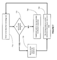
- FIG. 5 illustrates a flowchart depiction of the process of examining the conditions relating to processing of the semiconductor wafers.
- the production data which includes the manufacturing data and the environmental data associated with a particular manufacturing lot of semiconductor wafers, is analyzed, as described in block 510 .
- a determination is made whether there are out-of-control events during the manufacturing process of a particular semiconductor wafer, as described in block 520 of FIG. 5 .
- Out-of-control events during a semiconductor wafer manufacturing process include process events, such as over-exposure during photolithography processes, over-etching during etch processes, and the like.
- a conclusion is made that some excursion in the process is found, as described in block 530 of FIG. 5 .
- SPC Statistical Process Control
- SPC analysis is comprised of four main steps. The main steps of SPC analysis include measuring the process, reducing variances in the process to make the process more consistent, monitoring the process, and improving the process to produce its best value.
- real-time SPC which can be used for run-to-run control applications in one embodiment, data is collected from the most recently finished manufacturing run of semiconductor wafers before the next manufacturing run of semiconductor wafers is processed. Steps are taken to ensure that the quality of the processed semiconductor wafers is as consistent as possible from one manufacturing run to another.
- SPC analysis rules dictate that causes of errors discovered during one manufacturing run of semiconductor wafers must be corrected before the next manufacturing run of semiconductor wafers is performed.
- manufacturing alarms are used to indicate that an unacceptable level in a manufacturing environmental factor is present. For example, an alarm will be activated when the relative pressure is excessively high during a process. Another alarm will be activated when the ambient temperature during a process is too high or too low. Likewise, another alarm will be activated when the relative humidity in the manufacturing area is too high during a process run of semiconductor wafers. In one embodiment, an alarm will be activated when there is an unacceptable level of nitrogen-bearing gases present during a process.
- the processing of semiconductor wafers is continued, as described in block 450 of FIG. 4 .
- an automated test wafer generation process is performed, as described in block 460 of FIG. 4. A more detailed depiction of the steps used to perform the automated test wafer generation process is illustrated in FIG. 6 .
- a child lot that represents a set of test wafers 310 is acquired, as illustrated in block 610 of FIG. 6 .
- a set of predetermined test wafers 310 that are generally scattered though a particular lot of semiconductor wafers are acquired.
- one of a plurality of methods known by those skilled in the art is employed to move the test wafers 310 from the normal production line onto a test site.
- test wafers 310 When the test wafers 310 are acquired, they are sent to a metrology tool 150 for acquisition of metrology data, as described in block 620 of FIG. 6 . Once the metrology data associated with the test wafers 310 is acquired, the metrology data is stored and correlated with the corresponding production data, as described in block 630 of FIG. 6 . In one embodiment, the metrology data is processed by the metrology data processing unit 145 and stored into the memory of the computer system 130 . Generally, the errors found on the test wafers 310 can be attributed to the remainder of the lot of semiconductor wafers. If the metrology data indicates that there are significant process errors, the main processing of the corresponding semiconductor wafers is suspended, as described in block 640 of FIG. 6 .
- a process feedback system in the APC framework would generally be capable of correcting the error.
- a sustained disturbance is generally more serious wherein the feedback system in the APC framework would correct the error in an acceptably long period of time. In some cases the feedback system in the APC framework may not be able to correct the error at all due to several reasons, including the fact that the data received by the APC framework may be incorrect.
- the process may be modified, adjustments to the processing tools 110 , 112 may be made, modifications to the manufacturing model 140 may be performed, or other significant changes to the process system may be made, as described in block 660 of FIG. 6 .
- the aforementioned changes to the system are made in order to reduce the effects to the sustained disturbance.
- the acquired metrology data is processed and made ready to be used for feedback control, as described in block 670 .
- the completion of the step described in block 670 completes the step of performing automated test wafer generation process described in block 460 of FIG. 4 .
- a control parameter modification sequence is performed, as described in block 470 of FIG. 4 .
- FIG. 7 One embodiment of performing the control parameter modification sequence is illustrated in FIG. 7 .
- error data from the metrology data related to processed semiconductor wafers is acquired, as described in block 710 .
- the step described in block 720 is performed to determine whether an error is sufficiently significant to warrant a change in the control inputs on the line 120 .
- the errors acquired from product analysis stations are compared to a predetermined set of threshold parameters.
- the deadband contains a range of error values associated with control input signals centered proximate to a set of corresponding predetermined target values, for which generally controller action is blocked.
- any one of the errors acquired from the product analysis station is smaller than its corresponding predetermined threshold value, that particular error is deemed to be in the deadband.
- One of the primary purposes of the deadband is to prevent excessive control actions, resulting from changes to control input signals on the line 120 , from causing a semiconductor manufacturing process to be inordinately jittery.
- a manufacturing lot of semiconductor wafers are processed, as described in block 810 of FIG. 8 .
- An appropriate maximum jeopardy value for the manufacturing lot of semiconductor wafers is determined, as described in block 820 of FIG. 8 .
- the maximum jeopardy value generally represents the amount of semiconductor wafers that can be processed without any one of the processed wafers being further tested for errors. For example, if ten lots of semiconductor wafers are processed without measuring them or acquiring metrology data, the jeopardy is equal to ten lots. Limits are generally placed upon the maximum jeopardy value before measurement of a lot and feedback is performed.
- processing of the semiconductor wafers is continued.
- the automated test wafer generation process described in FIG. 6 is performed, as described in block 840 of FIG. 8 .
- the automated test wafer generation process described in FIG. 6 is described above.
- a control parameter modification sequence is initiated, as described in block 850 of FIG. 8 .
- the control parameter modification sequence described in block 850 is illustrated by the steps described in FIG. 7, which are described above.
- the principles taught by the present invention can be implemented in an Advanced Process Control (APC) Framework.
- the APC is a preferred platform from which to implement the overlay control and etch process control strategy taught by the present invention.
- the APC can be a factory-wide software system, therefore, the control strategies taught by the present invention can be applied to virtually any of the semiconductor manufacturing tools on the factory floor.
- the APC framework also allows for remote access and monitoring of the process performance. Furthermore, by utilizing the APC framework, data storage can be more convenient, more flexible, and less expensive than local drives.
- the APC platform allows for more sophisticated types of control because it provides a significant amount of flexibility in writing the necessary software code.
- Deployment of the control strategy taught by the present invention onto the APC framework could require a number of software components.
- a computer script is written for each of the semiconductor manufacturing tools involved in the control system.
- a semiconductor manufacturing tool in the control system When a semiconductor manufacturing tool in the control system is started in the semiconductor manufacturing fab, it generally calls upon a script to initiate the action that is required by the process controller, such as the overlay controller and etch process controller.
- the control methods are generally defined and performed in these scripts. The development of these scripts can comprise a significant portion of the development of a control system.
Abstract
Description
Claims (25)
Priority Applications (1)
| Application Number | Priority Date | Filing Date | Title |
|---|---|---|---|
| US09/577,403 US6647309B1 (en) | 2000-05-22 | 2000-05-22 | Method and apparatus for automated generation of test semiconductor wafers |
Applications Claiming Priority (1)
| Application Number | Priority Date | Filing Date | Title |
|---|---|---|---|
| US09/577,403 US6647309B1 (en) | 2000-05-22 | 2000-05-22 | Method and apparatus for automated generation of test semiconductor wafers |
Publications (1)
| Publication Number | Publication Date |
|---|---|
| US6647309B1 true US6647309B1 (en) | 2003-11-11 |
Family
ID=29401743
Family Applications (1)
| Application Number | Title | Priority Date | Filing Date |
|---|---|---|---|
| US09/577,403 Expired - Lifetime US6647309B1 (en) | 2000-05-22 | 2000-05-22 | Method and apparatus for automated generation of test semiconductor wafers |
Country Status (1)
| Country | Link |
|---|---|
| US (1) | US6647309B1 (en) |
Cited By (23)
| Publication number | Priority date | Publication date | Assignee | Title |
|---|---|---|---|---|
| US20020049565A1 (en) * | 1998-03-19 | 2002-04-25 | Kirila Gene E. | Process and device to continuously monitor and control a manufacturing process |
| US20040082083A1 (en) * | 2002-10-28 | 2004-04-29 | Vladimir Kraz | Process parameter event monitoring system and method for process |
| US20040241885A1 (en) * | 2002-11-12 | 2004-12-02 | Jorn Maeritz | Method, device, computer-readable storage medium and computer program element for the monitoring of a manufacturing process of a plurality of physical objects |
| US20040243456A1 (en) * | 2002-11-12 | 2004-12-02 | Jorn Maeritz | Method, device, computer-readable storage medium and computer program element for the monitoring of a manufacturing process of a plurality of physical objects |
| US20050015176A1 (en) * | 2003-02-18 | 2005-01-20 | Tokyo Electron Limited | Method for automatic configuration of processing system |
| US20050192698A1 (en) * | 2004-02-26 | 2005-09-01 | Chang Yung Cheng | Method and system for improving process control for semiconductor manufacturing operations |
| US20090168044A1 (en) * | 2007-12-27 | 2009-07-02 | Nuflare Technology, Inc. | Lithography apparatus and lithography method |
| US20090292506A1 (en) * | 2004-07-10 | 2009-11-26 | Kla-Tencor Corporation | Methods of and apparatuses for maintenance, diagnosis, and optimization of processes |
| US20100051502A1 (en) * | 2008-09-04 | 2010-03-04 | 3M Innovative Properties Company | Carrier having integral detection and measurement of environmental parameters |
| US20100279435A1 (en) * | 2009-04-30 | 2010-11-04 | Applied Materials, Inc. | Temperature control of chemical mechanical polishing |
| US20120078410A1 (en) * | 2010-09-24 | 2012-03-29 | Nulogy Corporation | Method, system and apparatus for automatic quality control using a plurality of computers |
| US8856698B1 (en) * | 2013-03-15 | 2014-10-07 | Globalfoundries Inc. | Method and apparatus for providing metric relating two or more process parameters to yield |
| US8963552B2 (en) | 2012-04-26 | 2015-02-24 | 3M Innovative Properties Company | Electrostatic discharge event detector |
| DE102020131741A1 (en) | 2020-11-30 | 2022-06-02 | Heliatek Gmbh | Checking the quality of a patterning process for forming electronic components |
| US11446711B2 (en) | 2019-05-29 | 2022-09-20 | Applied Materials, Inc. | Steam treatment stations for chemical mechanical polishing system |
| US11577358B2 (en) | 2020-06-30 | 2023-02-14 | Applied Materials, Inc. | Gas entrainment during jetting of fluid for temperature control in chemical mechanical polishing |
| US11597052B2 (en) | 2018-06-27 | 2023-03-07 | Applied Materials, Inc. | Temperature control of chemical mechanical polishing |
| US11628478B2 (en) | 2019-05-29 | 2023-04-18 | Applied Materials, Inc. | Steam cleaning of CMP components |
| US11633833B2 (en) | 2019-05-29 | 2023-04-25 | Applied Materials, Inc. | Use of steam for pre-heating of CMP components |
| US11826872B2 (en) | 2020-06-29 | 2023-11-28 | Applied Materials, Inc. | Temperature and slurry flow rate control in CMP |
| US11833637B2 (en) | 2020-06-29 | 2023-12-05 | Applied Materials, Inc. | Control of steam generation for chemical mechanical polishing |
| US11897079B2 (en) | 2019-08-13 | 2024-02-13 | Applied Materials, Inc. | Low-temperature metal CMP for minimizing dishing and corrosion, and improving pad asperity |
| US11919123B2 (en) | 2020-06-30 | 2024-03-05 | Applied Materials, Inc. | Apparatus and method for CMP temperature control |
Citations (7)
| Publication number | Priority date | Publication date | Assignee | Title |
|---|---|---|---|---|
| US5655110A (en) * | 1995-02-13 | 1997-08-05 | Advanced Micro Devices, Inc. | Method for setting and adjusting process parameters to maintain acceptable critical dimensions across each die of mass-produced semiconductor wafers |
| US6166801A (en) * | 1998-07-14 | 2000-12-26 | Nova Measuring Instruments, Ltd. | Monitoring apparatus and method particularly useful in photolithographically processing substrates |
| US6171737B1 (en) * | 1998-02-03 | 2001-01-09 | Advanced Micro Devices, Inc. | Low cost application of oxide test wafer for defect monitor in photolithography process |
| US6177133B1 (en) * | 1997-12-10 | 2001-01-23 | Silicon Valley Group, Inc. | Method and apparatus for adaptive process control of critical dimensions during spin coating process |
| US6192287B1 (en) * | 1997-09-23 | 2001-02-20 | On-Line Technologies, Inc. | Method and apparatus for fault detection and control |
| US6255125B1 (en) * | 1999-03-26 | 2001-07-03 | Advanced Micro Devices, Inc. | Method and apparatus for compensating for critical dimension variations in the production of a semiconductor wafer |
| US6303395B1 (en) * | 1999-06-01 | 2001-10-16 | Applied Materials, Inc. | Semiconductor processing techniques |
-
2000
- 2000-05-22 US US09/577,403 patent/US6647309B1/en not_active Expired - Lifetime
Patent Citations (7)
| Publication number | Priority date | Publication date | Assignee | Title |
|---|---|---|---|---|
| US5655110A (en) * | 1995-02-13 | 1997-08-05 | Advanced Micro Devices, Inc. | Method for setting and adjusting process parameters to maintain acceptable critical dimensions across each die of mass-produced semiconductor wafers |
| US6192287B1 (en) * | 1997-09-23 | 2001-02-20 | On-Line Technologies, Inc. | Method and apparatus for fault detection and control |
| US6177133B1 (en) * | 1997-12-10 | 2001-01-23 | Silicon Valley Group, Inc. | Method and apparatus for adaptive process control of critical dimensions during spin coating process |
| US6171737B1 (en) * | 1998-02-03 | 2001-01-09 | Advanced Micro Devices, Inc. | Low cost application of oxide test wafer for defect monitor in photolithography process |
| US6166801A (en) * | 1998-07-14 | 2000-12-26 | Nova Measuring Instruments, Ltd. | Monitoring apparatus and method particularly useful in photolithographically processing substrates |
| US6255125B1 (en) * | 1999-03-26 | 2001-07-03 | Advanced Micro Devices, Inc. | Method and apparatus for compensating for critical dimension variations in the production of a semiconductor wafer |
| US6303395B1 (en) * | 1999-06-01 | 2001-10-16 | Applied Materials, Inc. | Semiconductor processing techniques |
Cited By (29)
| Publication number | Priority date | Publication date | Assignee | Title |
|---|---|---|---|---|
| US20020049565A1 (en) * | 1998-03-19 | 2002-04-25 | Kirila Gene E. | Process and device to continuously monitor and control a manufacturing process |
| US7038279B2 (en) * | 2002-10-28 | 2006-05-02 | Credence Technologies, Inc. | Process parameter event monitoring system and method for process |
| US20040082083A1 (en) * | 2002-10-28 | 2004-04-29 | Vladimir Kraz | Process parameter event monitoring system and method for process |
| US7348187B2 (en) * | 2002-11-12 | 2008-03-25 | Infineon Technologies Ag | Method, device, computer-readable storage medium and computer program element for the monitoring of a manufacturing process of a plurality of physical objects |
| US20040243456A1 (en) * | 2002-11-12 | 2004-12-02 | Jorn Maeritz | Method, device, computer-readable storage medium and computer program element for the monitoring of a manufacturing process of a plurality of physical objects |
| US20040241885A1 (en) * | 2002-11-12 | 2004-12-02 | Jorn Maeritz | Method, device, computer-readable storage medium and computer program element for the monitoring of a manufacturing process of a plurality of physical objects |
| US20050015176A1 (en) * | 2003-02-18 | 2005-01-20 | Tokyo Electron Limited | Method for automatic configuration of processing system |
| US7213478B2 (en) * | 2003-02-18 | 2007-05-08 | Tokyo Electron Limited | Method for automatic configuration of processing system |
| US20050192698A1 (en) * | 2004-02-26 | 2005-09-01 | Chang Yung Cheng | Method and system for improving process control for semiconductor manufacturing operations |
| US7010382B2 (en) * | 2004-02-26 | 2006-03-07 | Taiwan Semiconductor Manufacturing Co., Ltd. | Method and system for improving process control for semiconductor manufacturing operations |
| US20090292506A1 (en) * | 2004-07-10 | 2009-11-26 | Kla-Tencor Corporation | Methods of and apparatuses for maintenance, diagnosis, and optimization of processes |
| US8653487B2 (en) * | 2007-12-27 | 2014-02-18 | Nuflare Technology, Inc. | Lithography apparatus and lithography method |
| US20090168044A1 (en) * | 2007-12-27 | 2009-07-02 | Nuflare Technology, Inc. | Lithography apparatus and lithography method |
| US20100051502A1 (en) * | 2008-09-04 | 2010-03-04 | 3M Innovative Properties Company | Carrier having integral detection and measurement of environmental parameters |
| US20100279435A1 (en) * | 2009-04-30 | 2010-11-04 | Applied Materials, Inc. | Temperature control of chemical mechanical polishing |
| US20120078410A1 (en) * | 2010-09-24 | 2012-03-29 | Nulogy Corporation | Method, system and apparatus for automatic quality control using a plurality of computers |
| US9471891B2 (en) * | 2010-09-24 | 2016-10-18 | Nulogy Corporation | Method, system and apparatus for automatic quality control using a plurality of computers |
| US8963552B2 (en) | 2012-04-26 | 2015-02-24 | 3M Innovative Properties Company | Electrostatic discharge event detector |
| US8856698B1 (en) * | 2013-03-15 | 2014-10-07 | Globalfoundries Inc. | Method and apparatus for providing metric relating two or more process parameters to yield |
| US11597052B2 (en) | 2018-06-27 | 2023-03-07 | Applied Materials, Inc. | Temperature control of chemical mechanical polishing |
| US11633833B2 (en) | 2019-05-29 | 2023-04-25 | Applied Materials, Inc. | Use of steam for pre-heating of CMP components |
| US11446711B2 (en) | 2019-05-29 | 2022-09-20 | Applied Materials, Inc. | Steam treatment stations for chemical mechanical polishing system |
| US11628478B2 (en) | 2019-05-29 | 2023-04-18 | Applied Materials, Inc. | Steam cleaning of CMP components |
| US11897079B2 (en) | 2019-08-13 | 2024-02-13 | Applied Materials, Inc. | Low-temperature metal CMP for minimizing dishing and corrosion, and improving pad asperity |
| US11826872B2 (en) | 2020-06-29 | 2023-11-28 | Applied Materials, Inc. | Temperature and slurry flow rate control in CMP |
| US11833637B2 (en) | 2020-06-29 | 2023-12-05 | Applied Materials, Inc. | Control of steam generation for chemical mechanical polishing |
| US11577358B2 (en) | 2020-06-30 | 2023-02-14 | Applied Materials, Inc. | Gas entrainment during jetting of fluid for temperature control in chemical mechanical polishing |
| US11919123B2 (en) | 2020-06-30 | 2024-03-05 | Applied Materials, Inc. | Apparatus and method for CMP temperature control |
| DE102020131741A1 (en) | 2020-11-30 | 2022-06-02 | Heliatek Gmbh | Checking the quality of a patterning process for forming electronic components |
Similar Documents
| Publication | Publication Date | Title |
|---|---|---|
| US6647309B1 (en) | Method and apparatus for automated generation of test semiconductor wafers | |
| US6465263B1 (en) | Method and apparatus for implementing corrected species by monitoring specific state parameters | |
| US6442496B1 (en) | Method and apparatus for dynamic sampling of a production line | |
| US8676538B2 (en) | Adjusting weighting of a parameter relating to fault detection based on a detected fault | |
| US8017411B2 (en) | Dynamic adaptive sampling rate for model prediction | |
| US6560503B1 (en) | Method and apparatus for monitoring controller performance using statistical process control | |
| US6460002B1 (en) | Method and apparatus for data stackification for run-to-run control | |
| US6773931B2 (en) | Dynamic targeting for a process control system | |
| US6560506B2 (en) | Method and apparatus for control for semiconductor processing for reducing effects of environmental effects | |
| US6337217B1 (en) | Method and apparatus for improved focus in optical processing | |
| US20050021272A1 (en) | Method and apparatus for performing metrology dispatching based upon fault detection | |
| JP2003519921A (en) | Process control system | |
| US6954883B1 (en) | Method and apparatus for performing fault detection using data from a database | |
| US6597447B1 (en) | Method and apparatus for periodic correction of metrology data | |
| US6947803B1 (en) | Dispatch and/or disposition of material based upon an expected parameter result | |
| US6905895B1 (en) | Predicting process excursions based upon tool state variables | |
| US6834213B1 (en) | Process control based upon a metrology delay | |
| US6890773B1 (en) | Dynamic maintenance of manufacturing system components | |
| US6697691B1 (en) | Method and apparatus for fault model analysis in manufacturing tools | |
| US6834211B1 (en) | Adjusting a trace data rate based upon a tool state | |
| US6871114B1 (en) | Updating process controller based upon fault detection analysis | |
| US7720559B1 (en) | Dynamic tool scheduling based upon defects | |
| US6823231B1 (en) | Tuning of a process control based upon layer dependencies | |
| US6912436B1 (en) | Prioritizing an application of correction in a multi-input control system | |
| US6689521B1 (en) | Method and apparatus for control of photoresist plasma removal |
Legal Events
| Date | Code | Title | Description |
|---|---|---|---|
| AS | Assignment |
Owner name: ADVANCED MICRO DEVICES, INC., TEXAS Free format text: ASSIGNMENT OF ASSIGNORS INTEREST;ASSIGNOR:BODE, CHRISTOPHER A.;REEL/FRAME:010819/0587 Effective date: 20000519 |
|
| STCF | Information on status: patent grant |
Free format text: PATENTED CASE |
|
| FPAY | Fee payment |
Year of fee payment: 4 |
|
| AS | Assignment |
Owner name: GLOBALFOUNDRIES INC., CAYMAN ISLANDS Free format text: AFFIRMATION OF PATENT ASSIGNMENT;ASSIGNOR:ADVANCED MICRO DEVICES, INC.;REEL/FRAME:023119/0083 Effective date: 20090630 |
|
| FPAY | Fee payment |
Year of fee payment: 8 |
|
| FPAY | Fee payment |
Year of fee payment: 12 |
|
| AS | Assignment |
Owner name: WILMINGTON TRUST, NATIONAL ASSOCIATION, DELAWARE Free format text: SECURITY AGREEMENT;ASSIGNOR:GLOBALFOUNDRIES INC.;REEL/FRAME:049490/0001 Effective date: 20181127 |
|
| AS | Assignment |
Owner name: GLOBALFOUNDRIES INC., CAYMAN ISLANDS Free format text: RELEASE BY SECURED PARTY;ASSIGNOR:WILMINGTON TRUST, NATIONAL ASSOCIATION;REEL/FRAME:054636/0001 Effective date: 20201117 |
|
| AS | Assignment |
Owner name: GLOBALFOUNDRIES U.S. INC., NEW YORK Free format text: RELEASE BY SECURED PARTY;ASSIGNOR:WILMINGTON TRUST, NATIONAL ASSOCIATION;REEL/FRAME:056987/0001 Effective date: 20201117 |