US6658144B1 - Diffraction tomography for monitoring latent image formation - Google Patents
Diffraction tomography for monitoring latent image formation Download PDFInfo
- Publication number
- US6658144B1 US6658144B1 US09/083,447 US8344798A US6658144B1 US 6658144 B1 US6658144 B1 US 6658144B1 US 8344798 A US8344798 A US 8344798A US 6658144 B1 US6658144 B1 US 6658144B1
- Authority
- US
- United States
- Prior art keywords
- latent image
- angle
- calculating
- diffracted
- function
- Prior art date
- Legal status (The legal status is an assumption and is not a legal conclusion. Google has not performed a legal analysis and makes no representation as to the accuracy of the status listed.)
- Expired - Lifetime
Links
Images


Classifications
-
- G—PHYSICS
- G01—MEASURING; TESTING
- G01N—INVESTIGATING OR ANALYSING MATERIALS BY DETERMINING THEIR CHEMICAL OR PHYSICAL PROPERTIES
- G01N23/00—Investigating or analysing materials by the use of wave or particle radiation, e.g. X-rays or neutrons, not covered by groups G01N3/00 – G01N17/00, G01N21/00 or G01N22/00
- G01N23/20—Investigating or analysing materials by the use of wave or particle radiation, e.g. X-rays or neutrons, not covered by groups G01N3/00 – G01N17/00, G01N21/00 or G01N22/00 by using diffraction of the radiation by the materials, e.g. for investigating crystal structure; by using scattering of the radiation by the materials, e.g. for investigating non-crystalline materials; by using reflection of the radiation by the materials
-
- G—PHYSICS
- G06—COMPUTING; CALCULATING OR COUNTING
- G06T—IMAGE DATA PROCESSING OR GENERATION, IN GENERAL
- G06T11/00—2D [Two Dimensional] image generation
- G06T11/003—Reconstruction from projections, e.g. tomography
- G06T11/006—Inverse problem, transformation from projection-space into object-space, e.g. transform methods, back-projection, algebraic methods
-
- Y—GENERAL TAGGING OF NEW TECHNOLOGICAL DEVELOPMENTS; GENERAL TAGGING OF CROSS-SECTIONAL TECHNOLOGIES SPANNING OVER SEVERAL SECTIONS OF THE IPC; TECHNICAL SUBJECTS COVERED BY FORMER USPC CROSS-REFERENCE ART COLLECTIONS [XRACs] AND DIGESTS
- Y10—TECHNICAL SUBJECTS COVERED BY FORMER USPC
- Y10S—TECHNICAL SUBJECTS COVERED BY FORMER USPC CROSS-REFERENCE ART COLLECTIONS [XRACs] AND DIGESTS
- Y10S977/00—Nanotechnology
- Y10S977/70—Nanostructure
- Y10S977/832—Nanostructure having specified property, e.g. lattice-constant, thermal expansion coefficient
- Y10S977/834—Optical properties of nanomaterial, e.g. specified transparency, opacity, or index of refraction
Definitions
- the present invention is related to integrated circuit manufacturing, and more particularly to the use of diffraction tomography for latent image metrology.
- Integrated circuits are manufactured through a sequence of controlled steps used to form layers of conducting, insulating and transistor-forming materials. Layers within the integrated circuit are formed by covering the surface of a wafer with photoresist and exposing selected portions of the photoresist to light at a particular wavelength.
- the exposure process begins when an exposing light source, traveling through a photomask containing the desired patterns, falls incident on the wafer.
- the photoresist is exposed to the light source traveling through the photomask, and depending on the photomask's geometry, the photoresist consequently undergoes gradual refractive index changes between the exposed region and the unexposed region.
- the changes in the photoresist due to exposure may not be visible at this point. That is why the image is termed a latent image.
- the photoresist is then developed and the unexposed areas are washed away.
- Latent image formation is a critical time in the manufacturing process. If the photoresist has been underexposed, the features formed in the developed photoresist may be too small to perform correctly. To date, the methods used to monitor latent image formation have been limited to either microscope inspection or diffraction measurement.
- Microscope inspection cannot be done real time. Microscope inspection typically requires a complicated setup. Furthermore, the wafer usually must be taken from the fab line to the microscope to be inspected.
- Diffraction measurement techniques used to date have been limited to heuristic approaches which correlate the intensity of diffractions to final critical dimension (CD) measurements. For instance, one would measure intensities of the first diffraction order and, after development of the photoresist, measure the resulting critical dimension. Such an approach is very inflexible. That is, any change to manufacturing parameters such as exposure intensity or duration, or in the chemistry of the photoresist, forces the manufacturer to go through the entire correlation process all over again.
- CD critical dimension
- the present invention is a system and method of reconstructing an image of a structure having periodic variations in index of refraction. Electromagnetic waves are projected onto the structure and the resulting diffracted electromagnetic waves are measured, wherein the step of measuring includes the step of determining a plurality of intensities DE. Refractive terms can then be calculated as a function of the intensities DE.
- latent image formation in photoresist can be measured by forming a periodic structure such as a grating in the photoresist. Light is projected onto the structure and the resulting diffracted light is measured, wherein the step of measuring includes the step of determining a plurality of intensities DE. Refractive terms can then be calculated as a function of the intensities DE.
- a stepper can be constructed which can monitor latent image formation in photoresist.
- the stepper includes a fixture for receiving a wafer and a photomask, a first light source for illuminating the wafer through the photomask and at a first incident angle, a second light source positioned to illuminate the wafer at a second incident angle, wherein the second angle is different from the first incident angle and a detector positioned to measure light diffracted from the wafer.
- a track can be constructed which can monitor latent image formation in photoresist.
- the track includes a bake chamber, a development chamber, a light source positioned to illuminate the wafer at an incident angle and a detector positioned to measure light diffracted from the wafer.
- FIG. 1 is a latent image measurement system according to the present invention
- FIG. 2 is an illustration of a two-dimensional latent image grating
- FIGS. 3 a - 3 c are alternate embodiments of the latent image measurement system of FIG. 1;
- FIG. 4 illustrates a stepper which includes a latent image measurement system
- FIG. 5 illustrates a track which includes a latent image measurement system
- FIG. 6 is an illustration of a two-dimensional latent image grating formed over a dielectric film
- FIG. 7 is a plot of the reconstructed index of refraction for various level of permitivity in the substrate region.
- FIG. 8 is an illustration of a three-dimensional latent image grating
- FIG. 11 is a flow chart of the reconstruction of a latent image.
- FIG. 1 illustrates a system for measuring latent image formation in a periodic structure such as a diffraction grating.
- System 10 includes a light source 12 and a detector 14 connected to a computer 16 .
- Light source 12 is used to illuminate wafer 18 in order to reconstruct the latent image formed inside the layer of photoresist coating wafer 18 .
- computer 16 controls light source 12 and uses the reflected light measured at detector 14 to reconstruct the pattern imaged onto the photoresist.
- the periodic structure could be a special diffraction grating formed in a section of the wafer, or it could be an approximately periodic structure identified within the device being manufactured on wafer 18 .
- the exposure process begins when an exposing light source, traveling through a photomask containing the desired patterns, is incident on wafer 18 .
- the photoresist is exposed to the light source traveling through the photomask, and depending on the photomask's geometry, the photoresist consequently undergoes gradual refractive index changes between the exposed region index, n 2 and the unexposed region index, n 1 .
- the photoresist is developed and the unexposed areas are washed away.
- the end result is a periodic train of pulses with refractive index n, period D, and width commonly referred to as critical dimension (CD).
- Diffraction tomography falls under the general area of inverse scattering.
- the purpose of inverse scattering is to reconstruct multidimensional objects from the subset of lower dimensional information or projections. This is accomplished by illuminating the objects at certain electromagnetic wavelengths from different directions and collecting the diffracted data or projections for inversion. Projections are defined generally as the mapping of an N-dimensional object to an (N ⁇ 1)-dimensional function by integrating the object on a particular path.
- the projection integration path mentioned above is application dependent.
- electromagnetic waves obey classical ray theory and propagate along straight lines through the object.
- the integration path is along straight lines and object reconstruction is accomplished via the well-known backprojection algorithm.
- the incident wavelength becomes comparable in dimension to the size of the object and the waves no longer travel in straight lines but experience diffraction.
- the integration path is semicircular.
- Different imaging algorithms for the diffracting case have been developed which fall under the following two categories: spatial domain algorithms, such as the backpropagation algorithm, and frequency domain algorithms, such as the Unified Fourier Reconstruction (UFR) algorithm.
- spatial domain algorithms such as the backpropagation algorithm
- frequency domain algorithms such as the Unified Fourier Reconstruction (UFR) algorithm.
- Diffraction tomography has been successfully applied to different areas such as medical imaging, geophysical sensing, and industrial inspection. Moreover, diffraction tomography can employ the reflected field, or the transmitted field, or both fields in its reconstructions depending on the application. When optical wavelengths are used, the technique is referred to as optical diffraction tomography (ODT).
- ODT optical diffraction tomography
- the most common application of ODT rests in the area of nondestructive evaluation. The goal is to reconstruct the refractive index profile of an object without affecting its optical properties.
- the incident field is usually a laser operating at nonexposing wavelengths.
- the system shown in FIG. 1 reconstructs periodic objects, known also as gratings, using reflected diffraction data.
- Previous and current work in ODT concentrated solely on reconstructing single aperiodic objects using transmitted diffraction data.
- the transmitted field is not readily available.
- the diffracted field is continuous.
- the periodic nature of the gratings used to study latent image formation restricts the diffracted field to reside in a discrete and finite number of propagating orders (orders 0, 1, ⁇ 1, etc.), thus limiting the number of available data points.
- the refractive index distribution of latent images can be reconstructed and the results used to control developed CD patterns.
- This technique requires as input the diffracted field, complex or magnitude, from latent images generated by a nonexposing source incident at different viewing angles.
- the ODT algorithm in turn produces at the output the reconstructed latent image.
- Region 1 is the input region with relative permittivity ⁇ 1 .
- Region 2 contains the grating denoted by its two-dimensional periodic complex refractive index distribution n(x, z), period D, and height W.
- Region 3 contains a substrate (e.g., silicon) having relative permittivity ⁇ 3 .
- the transmitted waves are absorbed as they propagate in region 3 through the substrate, hence limiting this technique to reflected waves only. In cases where the transmitted waves are available and detectable, they may be used in the reconstruction process. The transmitted waves, if available, can be used to improve the quality of the image reconstruction.
- u 1 ( x,y,z ) u i ( x,y,z )+ u d1 ( x,y,z ), (1)
- k x0 k 1 ⁇ 1 1 ⁇ 2 sin ⁇
- k z0 k 1 ⁇ 1 1 ⁇ 2 cos ⁇
- ⁇ is the angle of incidence
- ⁇ is the free-space wavelength
- R n is the complex reflection coefficient of the nth-order backward diffracted wave.
- T n is the complex transmission coefficient of the nth-order forward diffracted wave.
- R n s and T n s are calculated using different electromagnetic modeling techniques. This is known as the forward scattering problem.
- K is the magnitude of the grating vector.
- k zn ⁇ k 1 2 ⁇ ⁇ 1 - k xn 2 ; ⁇ k xn ⁇ ⁇ k 1 ⁇ ⁇ 1 j ⁇ k xn 2 - k 1 2 ⁇ ⁇ 1 ; ⁇ k xn ⁇ > k 1 ⁇ ⁇ 1 ( 4 )
- the real form of k zn corresponds to propagating waves, while the imaginary form corresponds to evanescent waves, i.e., damped waves traveling along the x axis. We are mainly interested in propagating waves.
- k zn3 ⁇ square root over (k 1 2 ⁇ 3 ⁇ k xn. 2 ) ⁇ (4)
- o ⁇ ⁇ ( x , z ) ⁇ o ⁇ ( x , z ) 0 ⁇ x ⁇ D 0 ; otherwise ( 7 )
- Equation (8) is a Fredholm integral equation of the second kind and is a solution to the diffracted field E d in both regions 1 and 3 .
- equation (8) It is not generally possible or desirable to directly solve for equation (8). Its solution may be computationally difficult for arbitrary o(x, z).
- One way of simplifying it is to linearize equation (8) through the use of linearizing approximations such as the weakly scattering or first Born approximation.
- the first Born approximation assumes that the diffracted field is much smaller than the incident field, and that, therefore,
- the first Rytov approximation can be used in a similar fashion to achieve a solution to the diffracted field E d .
- O ⁇ (K x ,K z ) is the two-dimensional Fourier transform of o ⁇ (x, z) in the (K x ,K z ) frequency plane and
- Equation (13) relates the two-dimensional Fourier transform of the object function to the one-dimensional complex reflection coefficients. It is also commonly referred to as the Fourier diffraction theorem. Therefore, from the complex reflection coefficients R n s of the Born approximation, the Fourier transform of the object is reconstructed as follows
- equations (14.1 and 14.2) the phase information is incorporated into the reconstruction process through the complex reflection coefficients, while equation (16) operates only on intensity data with no phase content.
- the diffraction efficiencies are estimated using either the first Born or Rytov approximations.
- Equation (22) k 1 2 ⁇ [ 1 - n 0 2 - 1 2 ⁇ n 1 2 - 2 ⁇ n 0 ⁇ n 1 ⁇ cos ⁇ ( 2 ⁇ ⁇ ⁇ ⁇ x D ) - n 1 2 2 ⁇ cos ⁇ ( 4 ⁇ ⁇ ⁇ ⁇ x D ) ] . ( 23 )
- Equation (28) can be used to solve both forward and inverse scattering problems in complex or magnitude form.
- equation (28) will be referred to as the Fourier Series Reconstruction (FSR) techniques.
- FSR Fourier Series Reconstruction
- Equation (28) was solved for different latent image gratings as illustrated in Table 1.
- n N ⁇ 1 the second highest modulation refractive term, n N ⁇ 1 , is determined from a measurement of the (2N ⁇ 1)th diffraction efficiency, DE 1(2N ⁇ 1). The process is thus continued until we reach the first modulation term, n 1 , which is determined from a measurement of the (N+1)th diffraction efficiency, DE 1(N ⁇ 1) , and estimates of the n 2 , n 3 , . . . nN ⁇ 1, n N refractive indices.
- n 1 the first modulation term
- N+2, N+1 diffraction orders to fully reconstruct the refractive index modulation factors.
- Diffraction orders below the N+1th diffraction order, i.e., N, N ⁇ 1, . . . ,2,1, contain redundant and ambiguous information on estimating the average refractive index, n 0 . Consequently, estimating n 0 from these diffraction orders should be performed with extreme caution; for an Nth order series expansion of n(x,z), there are N different ways of estimating n 0 .
- this technique appears to be well-suited for reconstructing the refractive index modulation values, n i s, in a slowly varying medium.
- this technique is applicable so long as the combination of period D and wavelength ⁇ is such that all the required diffraction orders are available.
- the average refractive index value, n 0 may be reconstructed using this technique; however, extreme caution must be employed when doing so, especially when the number of possible solutions becomes rather large (more than 2 solutions).
- FIG. 3 a illustrates another embodiment of a latent image measurement system 10 according to the present invention.
- light source 12 and detector 14 are mounted on a rail and can be moved to the desired Bragg angle under control of motor 30 .
- computer 16 controls motor 30 in order to position detector 14 and light source 12 .
- multiple fixed laser/detector apparatuses 38 are positioned at the desired Bragg angles as shown in FIG. 3 b below.
- Each apparatus 38 includes a light source 12 and a detector 14 .
- This latter configuration appears to have some advantages over that shown in FIG. 3 a , especially since there are no moving parts.
- the laser could operate at a fixed wavelength or be tunable to operate at multiple wavelengths.
- the desired diffracted order to be measured is anti-parallel to the incident wave, it may be difficult to separate between the incoming diffracted wave and the outgoing incident wave even in the presence of a beam splitter.
- One remedy would consist of placing the laser at an incident angle of ⁇ n ⁇ , where ⁇ n is the nth Bragg angle and ⁇ is a small angle increment. As a result, even though the nth diffracted wave still lies close to the incident wave, it is no longer anti-parallel to it and successful separation between both beams is possible.
- a light source (not shown) is mounted such that it can be moved to a number of different positions within semicircular arc 32 .
- a plurality of detectors 14 are fixedly mounted to positions along arc 32 .
- detectors 14 are mounted in an approximately continuous fashion along arc 32 . Such an approach can easily be adapted to changes in the anticipated Bragg angles due to changes in processing parameters.
- Latent image measurement system 10 can also be adapted to be part of the stepper or track so that it can be easily incorporated in the fab line.
- FIG. 4 shows a stepper 40 having an arc lamp 44 , a mirror 42 , a filter 46 , a condenser lens system 48 , an optical pattern transfer tool 50 and a lens reduction system 52 .
- Light from arc lamp 44 is reflected from mirror 42 and passes through filter 46 .
- Condenser lens system 48 focuses the light on optical pattern transfer tool 50 in order to transfer the pattern on tool 50 through reduction lens system 52 onto wafer 18 .
- Stepper 40 also includes a light source 12 and a detector 14 connected to a computer 16 .
- light source 12 and detector 14 operate at a different wavelength from arc lamp 44 in order to reduce interaction with the photoresist coating wafer 18 .
- the light source operates at a wavelength which causes a chemical change within the photoresist, the process is designed such that the added exposure is taken into account in determining exposure times and intensity.
- Light source 12 , detector 14 and computer 16 in stepper 40 cooperate to reconstruct an approximation to the latent image of a periodic structure on wafer 18 .
- the reconstructed approximation can then be used to control, for instance, arc lamp 44 in order to more finely tune the changes desired in the photoresist.
- latent image measurement system 10 can be adapted to a track 60 as is shown in FIG. 5 .
- Track 60 includes a tomographic chamber 62 , a bake chamber 63 and a development chamber 64 .
- Tomographic chamber 62 includes a light source 12 and a detector 14 connected to a computer 16 .
- Tomographic chamber 62 receives wafers 18 from a stepper upstream on the fab line and measures latent image formation as detailed above.
- light source 12 , detector 14 and computer 16 in track 60 cooperate to reconstruct an approximation to the latent image of a periodic structure on wafer 18 .
- light source 12 and detector 14 operate at a different wavelength from the light source used in the stepper upstream in order to reduce interaction with the photoresist coating wafer 18 .
- Bake chamber 63 includes a heating element used to heat wafer 18 to a desired temperature.
- Development chamber 64 includes a faucet 66 used to spray developer fluid 68 on the surface of wafer 18 .
- both development chamber 64 and bake chamber 63 receive wafers 18 from tomographic chamber 62 and use data from computer 16 to control baking and developing of the exposed photoresist.
- the reconstructed approximation of the periodic structure is used to control the development process in development chamber 64 in order to more finely tune the changes desired in the photoresist.
- n′ 1 as calculated by the FSR formulas for different ⁇ 3 values.
- the imaginary part of the refractive index in region 3 was negligible, so that the permittivity, ⁇ 3 was purely real.
- FIG. 7 that agreeable reconstructions for n′ 1 were obtained with an ⁇ 3 starting value of about 6. Below a value of 6, the reconstructions were inaccurate, which is of course due to the inability to incorporate the substrate's permittivity into the reflection tomography formulation.
- reconstructions from reflected waves under first order approximations can be deemed insensitive into the substrate region 3 .
- FIG. 8 The geometry of a three-dimensional latent image grating 80 is shown in FIG. 8 .
- An electric field, E i obliquely incident on the grating, produces both forward diffracted (transmitted) waves in region 3 and backward diffracted (reflected) waves in region 1 .
- the diffracted wave front in this case is two-dimensional along both the x and y directions.
- Region 1 is the input region with relative permittivity ⁇ 1 .
- Region 2 contains the grating denoted by its three-dimensional periodic complex refractive index distribution, n(x,y,z), periods, D x and D y along the x and y directions respectively, and height, or thickness, W.
- Region 3 contains the silicon substrate with relative permittivity ⁇ 3 .
- Equation (31) is the much sought FDT for reflection, for it relates the three-dimensional Fourier transform of the object function to the two-dimensional complex reflection coefficients. Therefore, from the complex reflection coefficients, R nm , the Fourier transform of the object function in the (K x ,K y ,K z ) frequency domain is reconstructed as follows
- DE 1nm is the diffraction efficiency of R nm in region 1 .
- Equation 36 defines the much sought FSR procedure for three-dimensional periodic structures, for it relates the two-dimensional exponential Fourier coefficients of the object function to the two-dimensional complex reflection coefficients.
- Equation (39) Substituting Equation (39) into the object function expression, which is given by
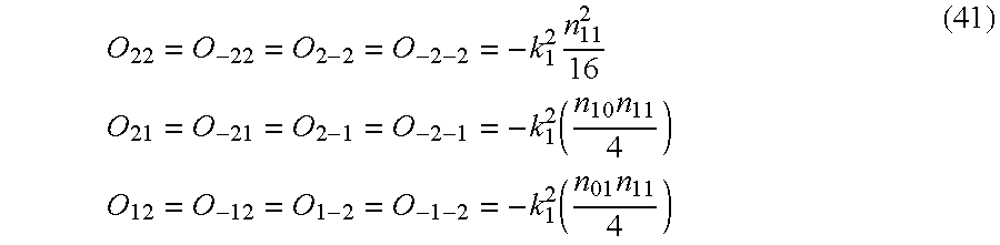
- n 11 256 ⁇ ⁇ ⁇ O 22 ⁇ 2 k 1 4 4 , ( 43 )
- n 10 and n 01 could have been alternatively determined from
- This nonuniqueness issue in determining the modulation refractive indices did not manifest itself for two-dimensional structures.
- the remaining Fourier coefficients can be used to determine the average refractive index n 00 in a nonunique manner.
- CDS critical dimension
- PEB post exposure bake
- ARC antireflecting
- the PEB process is performed on latent images prior to development in order to increase the chemical reaction rates.
- crucial control parameters for the PEB process such as bake time and temperature, to achieve the necessary conditions required for the desired final developed CDS.
- the diffraction tomography technique described above nondestructively reconstructs the refractive index distribution in latent images during and/or after exposure but prior to development.
- This technique requires as input the diffracted field, complex or magnitude, from latent images generated by nonexposing light sources.
- the reconstruction formulas in turn produce at the output reconstructed versions of the latent images.
- this technique is able to quantitatively determine the refractive index distributions occurring inside photoresists.
Abstract
Description


| TABLE 1 | ||
| ODT reconstruction results | ||
| Grating | Height, | Period, | Reconstructed | Reconstructed | ||
| parameters | W (μm) | D (μm) | n0 | n1 | ||
| n0 = 1.1, | 0.01 | 1.5 | 1.185 | 0.0097 | ||
| n1 = 0.01 | ||||||
| n0 = 1.2, | 0.01 | 1.5 | 1.291 | 0.0194 | ||
| n1 = 0.02 | ||||||
| n0 = 1.3, | 0.01 | 1.5 | 1.397 | 0.0292 | ||
| n1 = 0.03 | ||||||
| n0 = 1.4, | 0.01 | 1.5 | 1.503 | 0.0390 | ||
| n1 = 0.04 | ||||||
| n0 = 1.5, | 0.01 | 1.5 | 1.607 | 0.0489 | ||
| n1 = 0.05 | ||||||
| n0 = 1.6, | 0.01 | 1.5 | 1.711 | 0.0588 | ||
| n1 = 0.06 | ||||||
| n0 = 1.6, | 0.03 | 1.5 | 1.746 | 0.0726 | ||
| n1 = 0.06 | ||||||
| n0 = 1.6, | 0.05 | 1.5 | 1.870 | 0.1038 | ||
| n1 = 0.06 | ||||||
| n0 = 1.6, | 0.01 | 2.5 | 1.679 | 0.0610 | ||
| n1 = 0.06 | ||||||
| TABLE 2 | |||||
| N = 1 | N = 2 | N = 3 | N = 4 | ||
| O1 |
 |
 |
 |
 |
| O2 |
 |
 |
 |
 |
| O3 |
 |
 |
 |
|
| O4 |
 |
 |
 |
|
| O5 |
 |
 |
||
| O6 |
 |
 |
||
| O7 |
 |
|||
| O8 |
 |
|||


Claims (31)
Priority Applications (1)
| Application Number | Priority Date | Filing Date | Title |
|---|---|---|---|
| US09/083,447 US6658144B1 (en) | 1997-05-23 | 1998-05-22 | Diffraction tomography for monitoring latent image formation |
Applications Claiming Priority (2)
| Application Number | Priority Date | Filing Date | Title |
|---|---|---|---|
| US4753097P | 1997-05-23 | 1997-05-23 | |
| US09/083,447 US6658144B1 (en) | 1997-05-23 | 1998-05-22 | Diffraction tomography for monitoring latent image formation |
Publications (1)
| Publication Number | Publication Date |
|---|---|
| US6658144B1 true US6658144B1 (en) | 2003-12-02 |
Family
ID=29552502
Family Applications (1)
| Application Number | Title | Priority Date | Filing Date |
|---|---|---|---|
| US09/083,447 Expired - Lifetime US6658144B1 (en) | 1997-05-23 | 1998-05-22 | Diffraction tomography for monitoring latent image formation |
Country Status (1)
| Country | Link |
|---|---|
| US (1) | US6658144B1 (en) |
Cited By (9)
| Publication number | Priority date | Publication date | Assignee | Title |
|---|---|---|---|---|
| US20020009218A1 (en) * | 2000-04-28 | 2002-01-24 | Kenneth Chapman | Directional lighting and method to distinguish three dimensional information |
| US20030197859A1 (en) * | 2002-03-27 | 2003-10-23 | Takeo Kubota | Method of judging residual film by optical measurement |
| US20040090629A1 (en) * | 2002-11-08 | 2004-05-13 | Emmanuel Drege | Diffraction order selection for optical metrology simulation |
| US20040241561A1 (en) * | 2003-05-28 | 2004-12-02 | Li-Jui Chen | Scatterometric method of monitoring hot plate temperature and facilitating critical dimension control |
| US6867866B1 (en) * | 2001-08-10 | 2005-03-15 | Therma-Wave, Inc. | CD metrology analysis using green's function |
| US20050280810A1 (en) * | 2002-07-01 | 2005-12-22 | Johnson Kenneth C | Reduced multicubic database interpolation method for optical measurement of diffractive microstructures |
| US20060232768A1 (en) * | 2002-03-01 | 2006-10-19 | Borden Peter G | Evaluating a multi-layered structure for voids |
| US7489820B1 (en) * | 1998-09-14 | 2009-02-10 | Vdeh-Betriebsforschungsinstitut Gmbh | System for measuring the surface geometry and surface evenness of flat products |
| US10146140B2 (en) | 2015-10-12 | 2018-12-04 | Asml Netherlands B.V. | Methods and apparatus for simulating interaction of radiation with structures, metrology methods and apparatus, device manufacturing method |
Citations (14)
| Publication number | Priority date | Publication date | Assignee | Title |
|---|---|---|---|---|
| US4188123A (en) * | 1978-08-30 | 1980-02-12 | Rca Corporation | Optically measuring the carrier concentration in a semiconductor |
| US4408884A (en) * | 1981-06-29 | 1983-10-11 | Rca Corporation | Optical measurements of fine line parameters in integrated circuit processes |
| US4968108A (en) * | 1983-10-03 | 1990-11-06 | Fujitsu Limited | Method for constructing and reconstructing hologram |
| US5288572A (en) * | 1990-07-31 | 1994-02-22 | At&T Laboratories | Method for monitoring photoresist latent images |
| US5420680A (en) * | 1990-11-16 | 1995-05-30 | Ricoh Company, Ltd. | Method for measuring refractive index and thickness of film and apparatus therefor |
| US5594549A (en) * | 1992-06-04 | 1997-01-14 | Canon Kabushiki Kaisha | Position detecting method and projection exposure apparatus using the same |
| US5674652A (en) * | 1991-02-28 | 1997-10-07 | University Of New Mexico | Diffracted light from latent images in photoresist for exposure control |
| US5703692A (en) * | 1995-08-03 | 1997-12-30 | Bio-Rad Laboratories, Inc. | Lens scatterometer system employing source light beam scanning means |
| US5714750A (en) * | 1992-12-04 | 1998-02-03 | Psc Inc. | Bar code scanning and reading apparatus and diffractive light collection device suitable for use therein. |
| US5830611A (en) * | 1992-03-05 | 1998-11-03 | Bishop; Kenneth P. | Use of diffracted light from latent images in photoresist for optimizing image contrast |
| US5963315A (en) * | 1997-08-18 | 1999-10-05 | Motorola, Inc. | Method and apparatus for processing a semiconductor wafer on a robotic track having access to in situ wafer backside particle detection |
| US5968691A (en) * | 1997-01-30 | 1999-10-19 | Tokyo Electron Limited | Method and apparatus for coating resist and developing the coated resist |
| US5988502A (en) * | 1995-03-17 | 1999-11-23 | Symbol Technologies, Inc. | Electro-optical scanner having selectable scan pattern |
| US6005916A (en) * | 1992-10-14 | 1999-12-21 | Techniscan, Inc. | Apparatus and method for imaging with wavefields using inverse scattering techniques |
-
1998
- 1998-05-22 US US09/083,447 patent/US6658144B1/en not_active Expired - Lifetime
Patent Citations (14)
| Publication number | Priority date | Publication date | Assignee | Title |
|---|---|---|---|---|
| US4188123A (en) * | 1978-08-30 | 1980-02-12 | Rca Corporation | Optically measuring the carrier concentration in a semiconductor |
| US4408884A (en) * | 1981-06-29 | 1983-10-11 | Rca Corporation | Optical measurements of fine line parameters in integrated circuit processes |
| US4968108A (en) * | 1983-10-03 | 1990-11-06 | Fujitsu Limited | Method for constructing and reconstructing hologram |
| US5288572A (en) * | 1990-07-31 | 1994-02-22 | At&T Laboratories | Method for monitoring photoresist latent images |
| US5420680A (en) * | 1990-11-16 | 1995-05-30 | Ricoh Company, Ltd. | Method for measuring refractive index and thickness of film and apparatus therefor |
| US5674652A (en) * | 1991-02-28 | 1997-10-07 | University Of New Mexico | Diffracted light from latent images in photoresist for exposure control |
| US5830611A (en) * | 1992-03-05 | 1998-11-03 | Bishop; Kenneth P. | Use of diffracted light from latent images in photoresist for optimizing image contrast |
| US5594549A (en) * | 1992-06-04 | 1997-01-14 | Canon Kabushiki Kaisha | Position detecting method and projection exposure apparatus using the same |
| US6005916A (en) * | 1992-10-14 | 1999-12-21 | Techniscan, Inc. | Apparatus and method for imaging with wavefields using inverse scattering techniques |
| US5714750A (en) * | 1992-12-04 | 1998-02-03 | Psc Inc. | Bar code scanning and reading apparatus and diffractive light collection device suitable for use therein. |
| US5988502A (en) * | 1995-03-17 | 1999-11-23 | Symbol Technologies, Inc. | Electro-optical scanner having selectable scan pattern |
| US5703692A (en) * | 1995-08-03 | 1997-12-30 | Bio-Rad Laboratories, Inc. | Lens scatterometer system employing source light beam scanning means |
| US5968691A (en) * | 1997-01-30 | 1999-10-19 | Tokyo Electron Limited | Method and apparatus for coating resist and developing the coated resist |
| US5963315A (en) * | 1997-08-18 | 1999-10-05 | Motorola, Inc. | Method and apparatus for processing a semiconductor wafer on a robotic track having access to in situ wafer backside particle detection |
Non-Patent Citations (80)
| Title |
|---|
| Adams, T.E., "Applications of Latent Image Metrology in Microlithography", SPIE, 1464, pp. 294-312, (1991). |
| Bagchi, S., et al., "The nonuniform discrete fourier transform and its applications in filter design: Part I---1-D", IEEE, pp. 422-433, (Jun. 1996). |
| Baltes, H.P., et al., "Coherent and incoherent grating reconstruction", J. Opt. Soc. Am. A, 3(8), pp. 1268-1275, (Aug. 1986). |
| Baumbach, G.T., et al., "X-ray diffraction from epitaxial multilayered surface gratings", J. Phys. D: Appl. Phys., 28, pp. 2321-2327, (1995). |
| Bergossi, O., et al., "Visualization of latent images by reflection near field optical microscopy", Ultramicroscopy, 61, pp. 241-246, (1995). |
| Botten, L.C., "A new formalism for transmission gratings", Optica Acta, 25(6), pp. 481-499, (1978). |
| Bouzid, A., et al., "Scattering analysis of slanted fiber gratings", Applied Optics, 36(3), pp. 558-562, (Jan. 1997). |
| Box,, G.P., et al., "An Analysis of Transformation, 26(1)", Journal of the Royal Statistical Society, 26(1), pp. 211-252, (1964). |
| Burov, V.A., et al., "Diffraction tomography as an inverse scattering problem: the interpolation approach (linearized version)", Sov. Phys. Acoust., 38(4), pp. 349-355, (1992). |
| Carter, W.H., "On some diffraction effiency equations for a thick grating or hologram", Optics Communications, 103, pp. 1-7, (1993). |
| Devaney, A.J., "A Computer Simulation Study of Diffraction Tomography", IEEE Transactions on Biomedical Engineering, BME-30(7), pp. 377-386, (1983). |
| Devaney, A.J., "A Filtered Backpropagation Algorithm for Diffraction Tomography", Ultrasonic Imaging, 4, pp. 336-350, (1982). |
| Devaney, A.J., "Geophysical Diffraction Tomography", IEEE, pp. 3-13, (Jan. 1984). |
| Devaney, A.J., "Inverse scattering theory foundations of tomography with diffracting wavefields", SPIE, 768, International Symposium on Pattern Recognition and Acoustical Imaging, pp. 2-6, (1987). |
| Devaney, A.J., "Nonuniqueness in the inverse scattering problem", J. Math. Phys., 19(7), pp. 1526-1531, (Jul. 1978). |
| Fadda, E., et al., "Characterization of latent image by surface energy determined by contact angle measurements", Journal of Vacuum Science and Technology B, 13(3), pp. 1055-1057, (1995). |
| Fowles, G.R., Introduction to Modern Optics, Dover Publications Inc., New York, pp. 21-84, (1975). |
| Frolik, J.L., et al., "An Asymmetric Discrete-Time Approach for the Design and Analysis of Periodic Waveguide Gratings", Journal of Lightwave Technology, 13(2), pp. 175-185, (1995). |
| Garcia, N., et al., "Near-field optics inverse-scattering reconstruction of reflective surfaces", Optics Letters, 18924), pp. 2090-2092, (1993). |
| Gaylord, T.K., et al., "Analysis and Applications of Optical Diffraction by Gratings", Proceedings of the IEEE, 73(5), pp. 894-937, (May 1985). |
| Ghandi, S.K., VLSI Fabrication Principles, John Wiley & Sons Inc., New York, pp. 533-566, (1983). |
| Glytsis, E.N., et al., "Rigorous 3-D coupled wave diffraction analysis of multiple superposed gratings in anisotropic media", Applied Optics, 28(12), pp. 2401-2421, (Jun. 1989). |
| Goodman, J.W., Introduction to Fourier Optics, McGraw-Hill, San Francisco, pp. 57-75, (1968). |
| Gregus, J.A., et al., "Real-time latent image monitoring during holographic fabrication of submicron diffraction gratings", J. Vac. Sci. Technol. B, 11(6), pp. 2468-2472, (1993). |
| Gretzula, A., et al., "Structural measurement by inverse scattering in the Rytov approximation", J. Opt. Soc. Am., 2(11), pp. 1958-1960, (Nov. 1985). |
| Harthog, J., et al., "Thickness measurement for volume holograms by analysis of first-order diffraction", Applied Optics, 31(11), pp. 1803-1809, (Apr. 1992). |
| Hatab, Z., "Fourier Series Bases Diffraction Tomography Reconstruction of Multidimensional Gratings", Dissertation, University of New Mexico, Albuquerque, New Mexico, pp. 1-123, (May 1998). |
| Hatab, Z., et al., "Optical Diffraction Tomography for Latent Image Metrology", Poster presentation 1997 SPIE Conference, pp. 1-13, (Mar. 1997). |
| Hatab, Z.R., et al., "Optical diffraction tomography for latent image metrology", SPIE, 3050, pp. 515-524, (1997). |
| Hatab, Z.R., et al., "Sixteen-megabit dynamic random access memory trench depth characterization using two-dimensional diffraction analysis", J. Vac. Sci. Technol. B, 13(2), pp. 174-182, (1995). |
| Hickman, K.C., et al., "Use of diffracted light from latent images to improve lithography control", J. Vac. Sci. Technol. B, 10(5), pp. 2259-2266, (1992). |
| Joachimowicz, N., et al., "Inverse scattering: An iterative numerical method electromagnetic imaging", IEEE Transactions of Antennas and Propagation, 39(12), pp. 1742-1752, (1991). |
| Kak, A.C., et al., "Computerized Tomography with X-Ray, Emission and Ultrasound Sources", PRoceedings of the IEEE, 67(9), pp. 1245-1272, (Sep. 1979). |
| Kak, A.C., et al., Principles of Computerized Tomographic Imaging, IEEE Press, New York, pp. 203-273, (1988). |
| Kaveh, M., et al., "Signal Processing for Diffraction Tomography", IEEE Transactions on Sonics and Ultrasonics, SU-31(4), pp. 230-239, (Jul. 1984). |
| Kirsch, A., "Uniqueness theorems in inverse scattering theory for periodic structures", Inverse Problems, 10, pp. 145-152, (1994). |
| Kleemann, B.H., et al., "Integral equation method with parametrization of grating profile, Theory and experiments", Journal of Modern Optics, 43(7), pp. 1323-1349, (1996). |
| Koizumi, T., et al., "CD Control using Latent Image for Lithography", SPIE, 2439, pp. 418-426, (1995). |
| Lan, C., et al., "Plane-Scanning Reflection-Diffraction Tomography", IEEE Transactions on Sonics and Ultrasonics, SU-32(4), pp. 562-565, (Jul. 1985). |
| Lederer, F., et al., "Attenuated thick hologram gratings. Part I: Diffraction efficiency", Optical and Quantum Electronics, 9, pp 473-485, (1977). |
| Lin, F.C., et al., "Image Estimation from Scattered Field Data", International Journal of Imaging Systems and Technology, 2, pp. 76-95, (1990). |
| Ljunghdahl, G., et al., "Surface Scattering near Grazing Angles: The Distorted Wave Born Approximation for Rough Surfaces", Physics Scripta, 53, pp. 734-748, (1996). |
| Mack, C.A., "Absorption and exposure in positive photoresist", Applied Optics, 27(23), pp. 4913-4919, (Dec. 1988). |
| Marchman, H.M., et al., "Near field optical latent imaging with the photon tunneling microsope", Appl. Phys. Lett., 66(24), pp. 3269-3271, (1995). |
| Mersereau, R.M., et al., "Digital Reconstruction of Multidimensional Signals from Their Projection", Proceedings of the IEEE, 62(10), pp. 1319-1338, (Oct. 1974). |
| Milner, L.M., et al., "Stepper focus characterization using diffraction from latent images", J. Vac. Sci. Technol. B, 11(4), pp. 1258-1266, (1993). |
| Moharam, M.G., et al., "Criteria for bragg regime diffraction by phase gratings", Optics Communications, 32(1), pp. 14-18, (Jan. 1980). |
| Moharam, M.G., et al., "Diffraction analysis of dielectric surface-relief gratings", J. Opt. Soc. Am., 72(10), pp. 1385-1392, (1982). |
| Moharam, M.G., et al., "Rigorous coupled-wave analysis of grating diffraction -- E-mode polarization and losses", Opt. Soc. Am., 73(4), pp. 451-455, (1983). |
| Moharam, M.G., et al., "Rigorous coupled-wave analysis of metallic surface-relief gratings", J. Opt. Soc. Am. A, 3(11), pp. 1780-1787, (Nov. 1986). |
| Morris, J.B., et al., "Nonlinear filtering applied to single-view backpropagated images of strong scatterers", J. Opt. Soc. Am., 13(7), pp. 1506-1515, (Jul. 1996). |
| Murnane et al., Developed Photoresist Metrology using Scatterometry, Proc. SPIE vol. 2196, p. 47-59, May, 1994.* * |
| Ocola, L.E., et al., "Scanning force microscopy measurements of latent image topography in chemically amplified resists", Appl. Phys. Lett., 68(5), pp. 717-719, (1996). |
| Oppenheim, A.V., et al., Discrete-Time Signal Processing, Prentice-Hall, New Jersey, pp. 514-580, (1989). |
| Oppenheim, A.V., et al., Discrete-Time Signal Processing, Prentice-Hall, New Jersey, pp. 768-834, (1989). |
| Otto, G.P., et al., "Microwave inverse scattering----Local shape function imaging for improved resolution of strong scatterers", IEEE, pp. 137-141, (1994). |
| Pan, S.X., et al., "A computational study of reconstruction algorithms for diffraction tomography: Interpolation versus filtered backprogation", IEEE Transactions on Acoustics, Speech, and Signal Processing, ASSP-31(5), pp. 1262-1275, (Oct. 1983). |
| Paul, C.R., et al., "Introduction to Electromagnetic Fields", McGraw-Hill, New York, pp. 275-363, (1987). |
| Petit, R., Electromagnetic Theory of Gratings, Springer-Verlag, Barlin, pp. 1-41, (1980). |
| Rees, C.S., et al., Theory and Applications of Fourier Analysis, Marcel Dekker, Inc., New York, pp. 223-245, (1981). |
| Roger, A., et al., "Inverse scattering method in electromagnetic optics: Application to diffraction gratings", J. Opt. Soc. Am., 70(12), pp. 1483-1495, (1980). |
| Sabatier, P.C., et al., Basic Methods of Tomography and Inverse Problems, Adam Hilger, Bristol, pp. 125-467, (1987). |
| Sammar, A., et al., "Diffraction of multilayer gratings and zone plates in the X-ray region using the Born approximation", J. Opt. Soc. Am. A, 10(4), pp. 600-613, (Apr. 1993). |
| Shanmugan, K.S., et al., Random Signals: Detection, Estimation, and Data Analysis, John Wiley & Sons, New York, pg. 330, (1988). |
| Slaney, M., et al., "Limitations of Imaging with First-Order Diffraction Tomography", IEEE, pp. 860-874, (Aug. 1984). |
| Sohail, S., et al., "Analysis of a strip-grating twist reflector", J. Opt. Soc. Am. A, 7(9), pp. 1723-1729, (Sep. 1990). |
| Sohail, S., et al., "Diffractive techniques for lithographic process monitoring and concert", J. Vac. Sci. Technol. B, 12(6), pp. 3600-3606, (1994). |
| Stark, H., Image Recovery: Theory and Application, Academic Press, Inc., Orlando, pp. 369-413, (1987). |
| Steiglitz, K., et al., "Phase unwrapping by factorization", IEEE Transactions on Accoustics, Speech, and Signal Processing, ASSP-30(6), pp. 984-991, (Dec. 1982). |
| Sturtevant, J.L., et al., "Post-exposure bake as a process-control parameter for chemically-amplifide photoresist", SPIE, 1926, pp. 106-114, (1993). |
| Tenner, M.G., "A scanning optical microscope integrated in a wafer stepper for image sensing", SPIE, 2725, pp. 652-658, (1996). |
| Torolf C. Wedberg et al., Quantitative Microscopy of Phase Objects by Optical Diffraction Tomography, Proc. SPIE vol. 2083, p. 168-173, Feb. 1994.* * |
| Tribolet, J.M., "A New Phase Unwrapping Algorithm", IEEE Trasnactions on Acoustics, Speech, and Signal Processing, ASSP-25(2), pp. 170-177, (1977). |
| Wedberg, T.C., et al., "Experimental examination of the quantitative imaging properties of optical diffraction tomography", J. Opt. Soc. Am., 12(3), pp. 493-500, (Mar. 1995). |
| Werner J. Glantsching, How Accurately can one Reconstruct an Index Profile from Transverse Measurement Data, IEEE Journal of Lightwave Technology, vol. LT-3, No. 3, Jun. 1995, pp. 678-683.* * |
| Wolf, E., "Determination of the Amplitude and the Phase of Scattered Fields by Holography", Journal of the Optical Society of America, 60(1), pp. 18-20, (1970). |
| Wolf, E., "Three-dimensional structure dtermination of semi-transparent objects from holographic data", Optics Communications, 1(4), pp. 153-156, (Sep. 1969). |
| Yoon, E., et al., "Latent image diffraction from submicron photoresist gratings", J. Vac. Sci. Technol. B, 10(5), pp. 2230-2233, (1992). |
| Yoon, E., et al., "Phase-contrast latent image metrology for microlithography", SPIE, 1673, Integrated Circuit Metrology, Inspection, and Process Control VI, pp. 580-591, (1992). |
| Ziemer, R.E., et al., Signals and Systems: Continuous and Discrete, Macmillan Publishing Company, New York, pp. 83-130, (1989). |
Cited By (18)
| Publication number | Priority date | Publication date | Assignee | Title |
|---|---|---|---|---|
| US7489820B1 (en) * | 1998-09-14 | 2009-02-10 | Vdeh-Betriebsforschungsinstitut Gmbh | System for measuring the surface geometry and surface evenness of flat products |
| US20020009218A1 (en) * | 2000-04-28 | 2002-01-24 | Kenneth Chapman | Directional lighting and method to distinguish three dimensional information |
| US6901160B2 (en) * | 2000-04-28 | 2005-05-31 | Electro Scientific Industries | Directional lighting and method to distinguish three dimensional information |
| US6867866B1 (en) * | 2001-08-10 | 2005-03-15 | Therma-Wave, Inc. | CD metrology analysis using green's function |
| US20050137809A1 (en) * | 2001-08-10 | 2005-06-23 | Chang Yia C. | CD metrology analysis using green's function |
| US7038850B2 (en) | 2001-08-10 | 2006-05-02 | Therm-Wave, Inc. | CD metrology analysis using green's function |
| US7301619B2 (en) * | 2002-03-01 | 2007-11-27 | Applied Materials, Inc. | Evaluating a multi-layered structure for voids |
| US20060232768A1 (en) * | 2002-03-01 | 2006-10-19 | Borden Peter G | Evaluating a multi-layered structure for voids |
| US6984532B2 (en) * | 2002-03-27 | 2006-01-10 | Kabushiki Kaisha Toshiba | Method of judging residual film by optical measurement |
| US20030197859A1 (en) * | 2002-03-27 | 2003-10-23 | Takeo Kubota | Method of judging residual film by optical measurement |
| US20050280810A1 (en) * | 2002-07-01 | 2005-12-22 | Johnson Kenneth C | Reduced multicubic database interpolation method for optical measurement of diffractive microstructures |
| US7043397B2 (en) * | 2002-07-01 | 2006-05-09 | Tokyo Electron Limited | Reduced multicubic database interpolation method for optical measurement of diffractive microstructures |
| US20040090629A1 (en) * | 2002-11-08 | 2004-05-13 | Emmanuel Drege | Diffraction order selection for optical metrology simulation |
| US20040241561A1 (en) * | 2003-05-28 | 2004-12-02 | Li-Jui Chen | Scatterometric method of monitoring hot plate temperature and facilitating critical dimension control |
| US7135259B2 (en) * | 2003-05-28 | 2006-11-14 | Taiwan Semiconductor Manufacturing Co., Ltd. | Scatterometric method of monitoring hot plate temperature and facilitating critical dimension control |
| US20070068453A1 (en) * | 2003-05-28 | 2007-03-29 | Taiwan Semiconductor Manufacturing Co., Ltd. | Scatterometric method of monitoring hot plate temperature and facilitating critical dimension control |
| US7751025B2 (en) | 2003-05-28 | 2010-07-06 | Taiwan Semiconductor Manufacturing Co., Ltd. | Scatterometric method of monitoring hot plate temperature and facilitating critical dimension control |
| US10146140B2 (en) | 2015-10-12 | 2018-12-04 | Asml Netherlands B.V. | Methods and apparatus for simulating interaction of radiation with structures, metrology methods and apparatus, device manufacturing method |
Similar Documents
| Publication | Publication Date | Title |
|---|---|---|
| US9175951B2 (en) | Method and apparatus for determining structure parameters of microstructures | |
| US9804504B2 (en) | Method and apparatus for design of a metrology target | |
| US8731882B2 (en) | Methods and apparatus for modeling electromagnetic scattering properties of microscopic structures and methods and apparatus for reconstruction of microscopic structures | |
| US9766552B2 (en) | Methods and apparatus for calculating electromagnetic scattering properties of a structure and for reconstruction of approximate structures | |
| US7043397B2 (en) | Reduced multicubic database interpolation method for optical measurement of diffractive microstructures | |
| US7643666B2 (en) | Method and apparatus for angular-resolved spectroscopic lithography characterization | |
| US10408753B2 (en) | Method and apparatus for calculating electromagnetic scattering properties of finite periodic structures | |
| JP6924261B2 (en) | Hybrid weighing for characterizing patterned wafers | |
| US9939250B2 (en) | Methods and apparatus for calculating electromagnetic scattering properties of a structure and for estimation of geometrical and material parameters thereof | |
| TWI645178B (en) | Method and apparatus for calculating electromagnetic scattering properties of finite periodic structures | |
| CN106062634A (en) | Measuring a process parameter for a manufacturing process involving lithography | |
| US6658144B1 (en) | Diffraction tomography for monitoring latent image formation | |
| US8875078B2 (en) | Reference library generation method for methods of inspection, inspection apparatus and lithographic apparatus | |
| US8560270B2 (en) | Rational approximation and continued-fraction approximation approaches for computation efficiency of diffraction signals | |
| US20110276319A1 (en) | Determination of material optical properties for optical metrology of structures | |
| US7253909B1 (en) | Phase shift measurement using transmittance spectra | |
| Murnane et al. | Developed photoresist metrology using scatterometry | |
| US11041816B2 (en) | Methods and apparatus for calculating electromagnetic scattering properties of a structure and for reconstruction of approximate structures | |
| US20140297223A1 (en) | Method for using optical metrology to monitor critical dimension uniformity | |
| Wong et al. | Experimental and simulation studies of alignment marks | |
| Endres et al. | Numerical investigations of the influence of different commonly applied approximations in scatterometry | |
| Hatab et al. | Optical diffraction tomography for latent image metrology | |
| Hazart et al. | Robust sub-50-nm CD control by a fast-goniometric scatterometry technique | |
| Sohail et al. | First Principle Simulation of Diffraction based Metrology Techniques | |
| Henn et al. | On numerical reconstructions of lithographic masks in DUV scatterometry |
Legal Events
| Date | Code | Title | Description |
|---|---|---|---|
| AS | Assignment |
Owner name: MICRON TECHNOLOGY, INC., IDAHO Free format text: ASSIGNMENT OF ASSIGNORS INTEREST;ASSIGNOR:HATAB, ZIAD R.;REEL/FRAME:009189/0621 Effective date: 19980522 |
|
| STCF | Information on status: patent grant |
Free format text: PATENTED CASE |
|
| FEPP | Fee payment procedure |
Free format text: PAYOR NUMBER ASSIGNED (ORIGINAL EVENT CODE: ASPN); ENTITY STATUS OF PATENT OWNER: LARGE ENTITY |
|
| CC | Certificate of correction | ||
| FPAY | Fee payment |
Year of fee payment: 4 |
|
| FPAY | Fee payment |
Year of fee payment: 8 |
|
| FPAY | Fee payment |
Year of fee payment: 12 |
|
| AS | Assignment |
Owner name: U.S. BANK NATIONAL ASSOCIATION, AS COLLATERAL AGENT, CALIFORNIA Free format text: SECURITY INTEREST;ASSIGNOR:MICRON TECHNOLOGY, INC.;REEL/FRAME:038669/0001 Effective date: 20160426 Owner name: U.S. BANK NATIONAL ASSOCIATION, AS COLLATERAL AGEN Free format text: SECURITY INTEREST;ASSIGNOR:MICRON TECHNOLOGY, INC.;REEL/FRAME:038669/0001 Effective date: 20160426 |
|
| AS | Assignment |
Owner name: MORGAN STANLEY SENIOR FUNDING, INC., AS COLLATERAL AGENT, MARYLAND Free format text: PATENT SECURITY AGREEMENT;ASSIGNOR:MICRON TECHNOLOGY, INC.;REEL/FRAME:038954/0001 Effective date: 20160426 Owner name: MORGAN STANLEY SENIOR FUNDING, INC., AS COLLATERAL Free format text: PATENT SECURITY AGREEMENT;ASSIGNOR:MICRON TECHNOLOGY, INC.;REEL/FRAME:038954/0001 Effective date: 20160426 |
|
| AS | Assignment |
Owner name: U.S. BANK NATIONAL ASSOCIATION, AS COLLATERAL AGENT, CALIFORNIA Free format text: CORRECTIVE ASSIGNMENT TO CORRECT THE REPLACE ERRONEOUSLY FILED PATENT #7358718 WITH THE CORRECT PATENT #7358178 PREVIOUSLY RECORDED ON REEL 038669 FRAME 0001. ASSIGNOR(S) HEREBY CONFIRMS THE SECURITY INTEREST;ASSIGNOR:MICRON TECHNOLOGY, INC.;REEL/FRAME:043079/0001 Effective date: 20160426 Owner name: U.S. BANK NATIONAL ASSOCIATION, AS COLLATERAL AGEN Free format text: CORRECTIVE ASSIGNMENT TO CORRECT THE REPLACE ERRONEOUSLY FILED PATENT #7358718 WITH THE CORRECT PATENT #7358178 PREVIOUSLY RECORDED ON REEL 038669 FRAME 0001. ASSIGNOR(S) HEREBY CONFIRMS THE SECURITY INTEREST;ASSIGNOR:MICRON TECHNOLOGY, INC.;REEL/FRAME:043079/0001 Effective date: 20160426 |
|
| AS | Assignment |
Owner name: MICRON TECHNOLOGY, INC., IDAHO Free format text: RELEASE BY SECURED PARTY;ASSIGNOR:U.S. BANK NATIONAL ASSOCIATION, AS COLLATERAL AGENT;REEL/FRAME:047243/0001 Effective date: 20180629 |
|
| AS | Assignment |
Owner name: MICRON TECHNOLOGY, INC., IDAHO Free format text: RELEASE BY SECURED PARTY;ASSIGNOR:MORGAN STANLEY SENIOR FUNDING, INC., AS COLLATERAL AGENT;REEL/FRAME:050937/0001 Effective date: 20190731 |