US6664026B2 - Method of manufacturing high aspect ratio photolithographic features - Google Patents
Method of manufacturing high aspect ratio photolithographic features Download PDFInfo
- Publication number
- US6664026B2 US6664026B2 US09/815,540 US81554001A US6664026B2 US 6664026 B2 US6664026 B2 US 6664026B2 US 81554001 A US81554001 A US 81554001A US 6664026 B2 US6664026 B2 US 6664026B2
- Authority
- US
- United States
- Prior art keywords
- etch barrier
- barrier layer
- layer
- resist
- depositing
- Prior art date
- Legal status (The legal status is an assumption and is not a legal conclusion. Google has not performed a legal analysis and makes no representation as to the accuracy of the status listed.)
- Expired - Lifetime, expires
Links
- 238000004519 manufacturing process Methods 0.000 title description 5
- 238000000034 method Methods 0.000 claims abstract description 38
- 230000004888 barrier function Effects 0.000 claims abstract description 37
- 230000008569 process Effects 0.000 claims abstract description 32
- 239000000758 substrate Substances 0.000 claims abstract description 27
- 238000000151 deposition Methods 0.000 claims abstract description 16
- QVGXLLKOCUKJST-UHFFFAOYSA-N atomic oxygen Chemical compound [O] QVGXLLKOCUKJST-UHFFFAOYSA-N 0.000 claims abstract description 11
- 229910052760 oxygen Inorganic materials 0.000 claims abstract description 11
- 239000001301 oxygen Substances 0.000 claims abstract description 11
- OKTJSMMVPCPJKN-UHFFFAOYSA-N Carbon Chemical compound [C] OKTJSMMVPCPJKN-UHFFFAOYSA-N 0.000 claims abstract description 5
- 229910052799 carbon Inorganic materials 0.000 claims abstract description 5
- 229910003460 diamond Inorganic materials 0.000 claims abstract description 5
- 239000010432 diamond Substances 0.000 claims abstract description 5
- 239000000463 material Substances 0.000 claims description 16
- YCKRFDGAMUMZLT-UHFFFAOYSA-N Fluorine atom Chemical compound [F] YCKRFDGAMUMZLT-UHFFFAOYSA-N 0.000 claims description 9
- 229910052731 fluorine Inorganic materials 0.000 claims description 9
- 239000011737 fluorine Substances 0.000 claims description 9
- 229910052581 Si3N4 Inorganic materials 0.000 claims description 6
- VYPSYNLAJGMNEJ-UHFFFAOYSA-N Silicium dioxide Chemical compound O=[Si]=O VYPSYNLAJGMNEJ-UHFFFAOYSA-N 0.000 claims description 6
- HQVNEWCFYHHQES-UHFFFAOYSA-N silicon nitride Chemical compound N12[Si]34N5[Si]62N3[Si]51N64 HQVNEWCFYHHQES-UHFFFAOYSA-N 0.000 claims description 6
- 229910052814 silicon oxide Inorganic materials 0.000 claims description 6
- BPUBBGLMJRNUCC-UHFFFAOYSA-N oxygen(2-);tantalum(5+) Chemical compound [O-2].[O-2].[O-2].[O-2].[O-2].[Ta+5].[Ta+5] BPUBBGLMJRNUCC-UHFFFAOYSA-N 0.000 claims description 3
- 229910001936 tantalum oxide Inorganic materials 0.000 claims description 3
- 230000001939 inductive effect Effects 0.000 claims 1
- XUIMIQQOPSSXEZ-UHFFFAOYSA-N Silicon Chemical compound [Si] XUIMIQQOPSSXEZ-UHFFFAOYSA-N 0.000 abstract description 11
- 229910052710 silicon Inorganic materials 0.000 abstract description 11
- 239000010703 silicon Substances 0.000 abstract description 11
- 229920002120 photoresistant polymer Polymers 0.000 abstract description 3
- 238000001020 plasma etching Methods 0.000 abstract 1
- 238000012546 transfer Methods 0.000 description 6
- 238000007737 ion beam deposition Methods 0.000 description 3
- 229910052715 tantalum Inorganic materials 0.000 description 3
- GUVRBAGPIYLISA-UHFFFAOYSA-N tantalum atom Chemical compound [Ta] GUVRBAGPIYLISA-UHFFFAOYSA-N 0.000 description 3
- 238000013459 approach Methods 0.000 description 2
- 238000005229 chemical vapour deposition Methods 0.000 description 2
- 238000010276 construction Methods 0.000 description 2
- 230000008021 deposition Effects 0.000 description 2
- 229910052751 metal Inorganic materials 0.000 description 2
- 239000002184 metal Substances 0.000 description 2
- 229910001030 Iron–nickel alloy Inorganic materials 0.000 description 1
- 239000000956 alloy Substances 0.000 description 1
- 229910045601 alloy Inorganic materials 0.000 description 1
- 230000008901 benefit Effects 0.000 description 1
- 150000001721 carbon Chemical class 0.000 description 1
- 238000001311 chemical methods and process Methods 0.000 description 1
- 238000000224 chemical solution deposition Methods 0.000 description 1
- 239000004020 conductor Substances 0.000 description 1
- 238000007796 conventional method Methods 0.000 description 1
- 239000002178 crystalline material Substances 0.000 description 1
- 230000006872 improvement Effects 0.000 description 1
- 150000002500 ions Chemical class 0.000 description 1
- 230000003287 optical effect Effects 0.000 description 1
- 239000011368 organic material Substances 0.000 description 1
- 238000000206 photolithography Methods 0.000 description 1
- 238000007747 plating Methods 0.000 description 1
- 238000012545 processing Methods 0.000 description 1
- 239000004065 semiconductor Substances 0.000 description 1
- 238000007704 wet chemistry method Methods 0.000 description 1
- 238000004804 winding Methods 0.000 description 1
Images


Classifications
-
- G—PHYSICS
- G03—PHOTOGRAPHY; CINEMATOGRAPHY; ANALOGOUS TECHNIQUES USING WAVES OTHER THAN OPTICAL WAVES; ELECTROGRAPHY; HOLOGRAPHY
- G03F—PHOTOMECHANICAL PRODUCTION OF TEXTURED OR PATTERNED SURFACES, e.g. FOR PRINTING, FOR PROCESSING OF SEMICONDUCTOR DEVICES; MATERIALS THEREFOR; ORIGINALS THEREFOR; APPARATUS SPECIALLY ADAPTED THEREFOR
- G03F7/00—Photomechanical, e.g. photolithographic, production of textured or patterned surfaces, e.g. printing surfaces; Materials therefor, e.g. comprising photoresists; Apparatus specially adapted therefor
- G03F7/004—Photosensitive materials
- G03F7/09—Photosensitive materials characterised by structural details, e.g. supports, auxiliary layers
- G03F7/094—Multilayer resist systems, e.g. planarising layers
-
- H—ELECTRICITY
- H01—ELECTRIC ELEMENTS
- H01L—SEMICONDUCTOR DEVICES NOT COVERED BY CLASS H10
- H01L21/00—Processes or apparatus adapted for the manufacture or treatment of semiconductor or solid state devices or of parts thereof
- H01L21/02—Manufacture or treatment of semiconductor devices or of parts thereof
- H01L21/027—Making masks on semiconductor bodies for further photolithographic processing not provided for in group H01L21/18 or H01L21/34
- H01L21/033—Making masks on semiconductor bodies for further photolithographic processing not provided for in group H01L21/18 or H01L21/34 comprising inorganic layers
- H01L21/0332—Making masks on semiconductor bodies for further photolithographic processing not provided for in group H01L21/18 or H01L21/34 comprising inorganic layers characterised by their composition, e.g. multilayer masks, materials
-
- H—ELECTRICITY
- H01—ELECTRIC ELEMENTS
- H01L—SEMICONDUCTOR DEVICES NOT COVERED BY CLASS H10
- H01L21/00—Processes or apparatus adapted for the manufacture or treatment of semiconductor or solid state devices or of parts thereof
- H01L21/02—Manufacture or treatment of semiconductor devices or of parts thereof
- H01L21/04—Manufacture or treatment of semiconductor devices or of parts thereof the devices having at least one potential-jump barrier or surface barrier, e.g. PN junction, depletion layer or carrier concentration layer
- H01L21/0405—Manufacture or treatment of semiconductor devices or of parts thereof the devices having at least one potential-jump barrier or surface barrier, e.g. PN junction, depletion layer or carrier concentration layer the devices having semiconductor bodies comprising semiconducting carbon, e.g. diamond, diamond-like carbon
- H01L21/042—Changing their shape, e.g. forming recesses
-
- G—PHYSICS
- G03—PHOTOGRAPHY; CINEMATOGRAPHY; ANALOGOUS TECHNIQUES USING WAVES OTHER THAN OPTICAL WAVES; ELECTROGRAPHY; HOLOGRAPHY
- G03F—PHOTOMECHANICAL PRODUCTION OF TEXTURED OR PATTERNED SURFACES, e.g. FOR PRINTING, FOR PROCESSING OF SEMICONDUCTOR DEVICES; MATERIALS THEREFOR; ORIGINALS THEREFOR; APPARATUS SPECIALLY ADAPTED THEREFOR
- G03F7/00—Photomechanical, e.g. photolithographic, production of textured or patterned surfaces, e.g. printing surfaces; Materials therefor, e.g. comprising photoresists; Apparatus specially adapted therefor
- G03F7/26—Processing photosensitive materials; Apparatus therefor
- G03F7/40—Treatment after imagewise removal, e.g. baking
-
- G—PHYSICS
- G11—INFORMATION STORAGE
- G11B—INFORMATION STORAGE BASED ON RELATIVE MOVEMENT BETWEEN RECORD CARRIER AND TRANSDUCER
- G11B5/00—Recording by magnetisation or demagnetisation of a record carrier; Reproducing by magnetic means; Record carriers therefor
- G11B5/127—Structure or manufacture of heads, e.g. inductive
- G11B5/17—Construction or disposition of windings
-
- G—PHYSICS
- G11—INFORMATION STORAGE
- G11B—INFORMATION STORAGE BASED ON RELATIVE MOVEMENT BETWEEN RECORD CARRIER AND TRANSDUCER
- G11B5/00—Recording by magnetisation or demagnetisation of a record carrier; Reproducing by magnetic means; Record carriers therefor
- G11B5/127—Structure or manufacture of heads, e.g. inductive
- G11B5/31—Structure or manufacture of heads, e.g. inductive using thin films
- G11B5/3109—Details
- G11B5/3116—Shaping of layers, poles or gaps for improving the form of the electrical signal transduced, e.g. for shielding, contour effect, equalizing, side flux fringing, cross talk reduction between heads or between heads and information tracks
-
- G—PHYSICS
- G11—INFORMATION STORAGE
- G11B—INFORMATION STORAGE BASED ON RELATIVE MOVEMENT BETWEEN RECORD CARRIER AND TRANSDUCER
- G11B5/00—Recording by magnetisation or demagnetisation of a record carrier; Reproducing by magnetic means; Record carriers therefor
- G11B5/127—Structure or manufacture of heads, e.g. inductive
- G11B5/31—Structure or manufacture of heads, e.g. inductive using thin films
- G11B5/3163—Fabrication methods or processes specially adapted for a particular head structure, e.g. using base layers for electroplating, using functional layers for masking, using energy or particle beams for shaping the structure or modifying the properties of the basic layers
Definitions
- This invention relates to a method of manufacturing photolithographic features which have high aspect ratios. This method is applicable to manufacturing devices such as recording heads for disk drives and semiconductor integrated circuits.
- Devices which are made with photolithographic processes include articles such as recording heads for disk drives and integrated circuits for a variety of applications. In general there is a trend to make such devices smaller and smaller.
- the important dimensions of such devices can include for example the track widths of recording heads and conductor widths for integrated circuits.
- the conventional photolithographic processes of manufacturing these small features involve first forming a layer of photo resist on a substrate such as metal or silicon. Then a pattern is created in the resist layer by first exposing through a patterned mask with the proper light for that particular resist and then chemically dissolving away the exposed portions of the resist to expose the underlying substrate. The actual structure in the final device is then usually constructed by plating or otherwise building the features onto the substrate. After the feature has been built, the remaining resist layer is removed.
- This conventional approach is appropriate when the width of the desired features is relatively large compared to the depth or thickness of the resist; or correspondingly, when the width of the features is large relative to the height of the feature.
- the aspect ratio of a feature is defined as the height of a feature divided by the width. For example, a recording head for very high density applications would have a very narrow track width and the height of the write pole would be large compared to the track width.
- An improvement in the conventional processes of achieving high aspect ratio features has been the use of an image transfer process.
- a thin adhesion layer typically containing a tantalum rich material is placed on the substrate to provide improved adhesion for the resist layer.
- a thin top layer of a silicon rich or tantalum rich material is placed on top of the resist layer, and a pattern is created in this top layer.
- an oxygen based reactive ion etch (RIE) is used to create the template in the resist layer.
- RIE reactive ion etch
- This method has the advantage of creating more sharply defined walls in the resist template (e.g. little undercutting).
- this approach has at least two noteworthy shortcomings.
- the adhesion layer material which is removed during the RIE process tends to deposit on the walls of the photoresist template.
- the present invention is a photolithographic process which includes a step of forming an effective etch barrier for an oxygen RIE process.
- the process results in improved protection of the substrate and more sharply defined goemetrical features.
- the steps of the process of the present invention include first placing a silicon rich thin layer on the substrate using a low energy deposition. A thin diamond like carbon (DLC) layer is then placed on the silicon rich layer. Relatively thick resist is then placed on the DLC. Finally the image transfer layers comprising a silicon rich or tantalum rich layer and an additional resist layer which is relatively thin are placed on the thicker resist. The DLC layer provides good adhesion with the resist.
- the silicon rich material on the substrate is the etch barrier which protects the substrate during the oxygen RIE. The silicon rich material is subsequently removed with a fluorine based RIE without damage to the substrate and with minimal redeposition on the walls of the features in the resist layer.
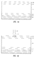
- FIG. 1 a shows the sequence of layers before the process steps resulting in a resist template.
- FIG. 1 b shows the first step of exposing a portion of the upper, then resist layer 106 .
- FIG. 1 c shows the result of removing the exposed sections of the thin resist layer 106 .
- FIG. 1 d shows the step of using a fluorine based RIE to transfer the pattern through the etch barrier 105 .
- FIG. 1 e shows the step of using an oxygen based RIE to transfer the pattern through the resits layer 104 and the DLC layer.
- FIG. 1 f shows using a flourine based RIE to remove the silicon rich layer 102 .
- FIG. 2 shows a coil structure of a magnetic recording write head made with the present invention.
- FIG. 1 shows a series of process steps illustrating the present invention.
- a sequence of layers formed on the substrate 101 Depending on the device, the substrate could be a substantially pure metal such as Cu or an alloy such as NiFe or CoNiFe. Additionally the substrate could be an amorphous crystalline material used in integrated circuit construction.
- a first etch barrier layer 102 of Si rich material is then placed on the substrate. This material could be relatively pure Si, but more commonly the material is silicon oxide, silicon nitride, or a combination thereof. This layer is typically in the thickness range of 10 to 40 Angstroms but is not limited to this range.
- the Si rich etch barrier layer 102 prevents oxygen RIE damage to the substrate.
- the next layer 103 is composed of diamond like carbon (DLC). This material is hydrogenated carbon which is relatively hard and durable. Typical thickness values for the DLC layer range from 20 to 60 Angstroms.
- the DLC layer 103 also functions as a very good adhesion layer with the first resist layer 104 .
- the resist layer material is conventional has no special requirements beyond conventional use.
- the thickness of the first resist layer 104 depends on the desired vertical dimension of the final feature. For example the pole of a magnet recording write head is typically from 1 to 4 um tall. If the desired pole height was 3 um, then the resist thickness would be about 3 um.
- the relatively thick resist layer 104 is placed on the DLC layer 103 .
- a relatively thin second etch barrier layer 105 is placed on the thick resist layer 104 .
- this thin layer 105 is to provide an protecting etch barrier to the resist layer 104 during the subsequent oxygen RIE process. Accordingly the material for this layer 105 is typically silicon oxide, silicon nitride, or tantalum oxide. The thickness of this layer 105 is not especially critical and is typically a few hundred Angstroms. Finally a thin layer of conventional resist 106 is placed on the etch barrier layer 105 . The thickness of this layer is usually substantially less than one micron.
- All of the layers are deposited using well known processes including spin coat, chemical solution deposition, or low energy chemical vapor deposition. It is usually important to form well defined, distinct interfaces between the substrate 101 and the Si rich layer 102 and also between the Si rich layer 102 and the DLC layer 103 . Accordingly it is preferable to use lower energy deposition techniques such as chemical vapor deposition rather than a higher energy technique such as ion beam deposition. A technique such as routine ion beam deposition tends to damage the substrate surface and to make the interfaces less distinct. However a lower energy ion beam deposition, where substrate damage is minimal is also acceptable. The subsequent RIE steps leave a cleaner, better defined surface if a low energy process is used for deposition.
- FIG. 1 b shows the first step of exposing a portion of the upper, thin resist layer 106 to light 107 through a mask to expose some areas of resist 108 . This light exposure step is typically done with an optical mask (not shown) which has the desired pattern or image.
- FIG. 1 c the exposed sections 108 of the thin resist 106 have been removed by developing the resist to leave a pattern 109 .
- FIG. 1 d shows the next step of using a fluorine based RIE 110 to transfer the pattern through the etch barrier 105 . The pattern 111 is then transfered to the top of the thick resist layer 104 . Fluorine based RIE is effective in removing Si materials whereas oxygen based RIE is effective in removing organic material.
- the next step is to use an oxygen based RIE 112 to transfer the pattern through the resist layer 104 and the DLC layer 103 in the patterned area 113 .
- This RIE step leaves walls 114 which are much more straight and well defined than by using the conventional chemical processes.
- the junction between the walls and the bottom layer 115 is also more sharply defined. This enables the construction of a more narrow feature and therefore a feature with a higher aspect ratio.
- the final step, illustrated in FIG. 1 f is to use a Fluorine based RIE 116 to remove the Si material under the pattern 117 in the silicon rich layer 102 .
- the well defined trenches which form the desired pattern or template are now ready to be filled with the desired material using any of the conventional processes.
- FIG. 2 shows an example of a structure made with the invented process.
- the structure in FIG. 2 is a coil winding for a write head used in magnetic recording.
- the coil height was about 3 um and was approximately determined by the thickness of the thicker resist 104 .
- the coil width was approximately 0.5 um resulting in an aspect ratio of about 6. This structure demonstrates that the well defined wall geometry and the sharp intersection of the wall and the substrate result in well defined final geometry of the constructed device.
Abstract
Description
Claims (14)
Priority Applications (1)
| Application Number | Priority Date | Filing Date | Title |
|---|---|---|---|
| US09/815,540 US6664026B2 (en) | 2001-03-22 | 2001-03-22 | Method of manufacturing high aspect ratio photolithographic features |
Applications Claiming Priority (1)
| Application Number | Priority Date | Filing Date | Title |
|---|---|---|---|
| US09/815,540 US6664026B2 (en) | 2001-03-22 | 2001-03-22 | Method of manufacturing high aspect ratio photolithographic features |
Publications (2)
| Publication Number | Publication Date |
|---|---|
| US20020136990A1 US20020136990A1 (en) | 2002-09-26 |
| US6664026B2 true US6664026B2 (en) | 2003-12-16 |
Family
ID=25218100
Family Applications (1)
| Application Number | Title | Priority Date | Filing Date |
|---|---|---|---|
| US09/815,540 Expired - Lifetime US6664026B2 (en) | 2001-03-22 | 2001-03-22 | Method of manufacturing high aspect ratio photolithographic features |
Country Status (1)
| Country | Link |
|---|---|
| US (1) | US6664026B2 (en) |
Cited By (20)
| Publication number | Priority date | Publication date | Assignee | Title |
|---|---|---|---|---|
| US20040075938A1 (en) * | 2002-04-02 | 2004-04-22 | Hitachi Global Storage Technologies | Magnetic head coil structure and method for manufacturing the same |
| US20040168586A1 (en) * | 2000-10-12 | 2004-09-02 | Board Of Regents, The University Of Texas System | Imprint lithography template having a feature size under 250 nm |
| US20050207741A1 (en) * | 2003-12-19 | 2005-09-22 | Carrier Corporation | Identification of electric heater capacity |
| US20050241140A1 (en) * | 2004-04-30 | 2005-11-03 | Hitachi Global Storage Technologies | High milling resistance write pole fabrication method for perpendicular recording |
| US20060000795A1 (en) * | 2004-06-30 | 2006-01-05 | Chen Tsung Y | Method for fabricating a pole tip in a magnetic transducer |
| US7140861B2 (en) | 2004-04-27 | 2006-11-28 | Molecular Imprints, Inc. | Compliant hard template for UV imprinting |
| US7179079B2 (en) | 2002-07-08 | 2007-02-20 | Molecular Imprints, Inc. | Conforming template for patterning liquids disposed on substrates |
| US20070243279A1 (en) * | 2005-01-31 | 2007-10-18 | Molecular Imprints, Inc. | Imprint Lithography Template to Facilitate Control of Liquid Movement |
| US7309225B2 (en) | 2004-08-13 | 2007-12-18 | Molecular Imprints, Inc. | Moat system for an imprint lithography template |
| US20080160129A1 (en) * | 2006-05-11 | 2008-07-03 | Molecular Imprints, Inc. | Template Having a Varying Thickness to Facilitate Expelling a Gas Positioned Between a Substrate and the Template |
| US7759407B2 (en) | 2005-07-22 | 2010-07-20 | Molecular Imprints, Inc. | Composition for adhering materials together |
| US7785526B2 (en) | 2004-07-20 | 2010-08-31 | Molecular Imprints, Inc. | Imprint alignment method, system, and template |
| US20100327404A1 (en) * | 2009-06-24 | 2010-12-30 | Harris Corporation | Inductor structures for integrated circuit devices |
| US7939131B2 (en) | 2004-08-16 | 2011-05-10 | Molecular Imprints, Inc. | Method to provide a layer with uniform etch characteristics |
| US7981481B2 (en) | 2004-09-23 | 2011-07-19 | Molecular Imprints, Inc. | Method for controlling distribution of fluid components on a body |
| US8179221B2 (en) * | 2010-05-20 | 2012-05-15 | Harris Corporation | High Q vertical ribbon inductor on semiconducting substrate |
| US8304855B2 (en) | 2010-08-04 | 2012-11-06 | Harris Corporation | Vertical capacitors formed on semiconducting substrates |
| US8557351B2 (en) | 2005-07-22 | 2013-10-15 | Molecular Imprints, Inc. | Method for adhering materials together |
| US8808808B2 (en) | 2005-07-22 | 2014-08-19 | Molecular Imprints, Inc. | Method for imprint lithography utilizing an adhesion primer layer |
| US9223202B2 (en) | 2000-07-17 | 2015-12-29 | Board Of Regents, The University Of Texas System | Method of automatic fluid dispensing for imprint lithography processes |
Citations (10)
| Publication number | Priority date | Publication date | Assignee | Title |
|---|---|---|---|---|
| US4589952A (en) * | 1982-07-03 | 1986-05-20 | International Business Machines Corporation | Method of making trenches with substantially vertical sidewalls in silicon through reactive ion etching |
| JPS6243650A (en) | 1985-08-21 | 1987-02-25 | Toray Ind Inc | Electrophotographic sensitive body |
| US5246884A (en) | 1991-10-30 | 1993-09-21 | International Business Machines Corporation | Cvd diamond or diamond-like carbon for chemical-mechanical polish etch stop |
| US5679269A (en) * | 1994-07-12 | 1997-10-21 | International Business Machines, Corp. | Diamond-like carbon for use in VLSI and ULSI interconnect systems |
| US5725573A (en) | 1994-03-29 | 1998-03-10 | Southwest Research Institute | Medical implants made of metal alloys bearing cohesive diamond like carbon coatings |
| US5780119A (en) | 1996-03-20 | 1998-07-14 | Southwest Research Institute | Treatments to reduce friction and wear on metal alloy components |
| US5985524A (en) | 1997-03-28 | 1999-11-16 | International Business Machines Incorporated | Process for using bilayer photoresist |
| US5989693A (en) | 1995-01-26 | 1999-11-23 | Optical Coating Laboratory, Inc. | Fluorine-containing abrasion-resistant optical thin film devices |
| US6030904A (en) | 1997-08-21 | 2000-02-29 | International Business Machines Corporation | Stabilization of low-k carbon-based dielectrics |
| US6156487A (en) * | 1998-10-23 | 2000-12-05 | Matsushita-Kotobuki Electronics Industries, Ltd. | Top surface imaging technique for top pole tip width control in magnetoresistive read/write head processing |
-
2001
- 2001-03-22 US US09/815,540 patent/US6664026B2/en not_active Expired - Lifetime
Patent Citations (10)
| Publication number | Priority date | Publication date | Assignee | Title |
|---|---|---|---|---|
| US4589952A (en) * | 1982-07-03 | 1986-05-20 | International Business Machines Corporation | Method of making trenches with substantially vertical sidewalls in silicon through reactive ion etching |
| JPS6243650A (en) | 1985-08-21 | 1987-02-25 | Toray Ind Inc | Electrophotographic sensitive body |
| US5246884A (en) | 1991-10-30 | 1993-09-21 | International Business Machines Corporation | Cvd diamond or diamond-like carbon for chemical-mechanical polish etch stop |
| US5725573A (en) | 1994-03-29 | 1998-03-10 | Southwest Research Institute | Medical implants made of metal alloys bearing cohesive diamond like carbon coatings |
| US5679269A (en) * | 1994-07-12 | 1997-10-21 | International Business Machines, Corp. | Diamond-like carbon for use in VLSI and ULSI interconnect systems |
| US5989693A (en) | 1995-01-26 | 1999-11-23 | Optical Coating Laboratory, Inc. | Fluorine-containing abrasion-resistant optical thin film devices |
| US5780119A (en) | 1996-03-20 | 1998-07-14 | Southwest Research Institute | Treatments to reduce friction and wear on metal alloy components |
| US5985524A (en) | 1997-03-28 | 1999-11-16 | International Business Machines Incorporated | Process for using bilayer photoresist |
| US6030904A (en) | 1997-08-21 | 2000-02-29 | International Business Machines Corporation | Stabilization of low-k carbon-based dielectrics |
| US6156487A (en) * | 1998-10-23 | 2000-12-05 | Matsushita-Kotobuki Electronics Industries, Ltd. | Top surface imaging technique for top pole tip width control in magnetoresistive read/write head processing |
Non-Patent Citations (1)
| Title |
|---|
| IBM Technical Bulletin Disclosure "Method for Slider Attachment and Head Termination to a Suspension in a Disk File", Feb. 1993, pp. 371-372. |
Cited By (35)
| Publication number | Priority date | Publication date | Assignee | Title |
|---|---|---|---|---|
| US9223202B2 (en) | 2000-07-17 | 2015-12-29 | Board Of Regents, The University Of Texas System | Method of automatic fluid dispensing for imprint lithography processes |
| US20040168586A1 (en) * | 2000-10-12 | 2004-09-02 | Board Of Regents, The University Of Texas System | Imprint lithography template having a feature size under 250 nm |
| US7229273B2 (en) | 2000-10-12 | 2007-06-12 | Board Of Regents, The University Of Texas System | Imprint lithography template having a feature size under 250 nm |
| US7304821B2 (en) * | 2002-04-02 | 2007-12-04 | Hitachi Global Storage Technologies Netherlands B.V. | Magnetic head coil structure and method for manufacturing the same |
| US20040075938A1 (en) * | 2002-04-02 | 2004-04-22 | Hitachi Global Storage Technologies | Magnetic head coil structure and method for manufacturing the same |
| US7699598B2 (en) | 2002-07-08 | 2010-04-20 | Molecular Imprints, Inc. | Conforming template for patterning liquids disposed on substrates |
| US7179079B2 (en) | 2002-07-08 | 2007-02-20 | Molecular Imprints, Inc. | Conforming template for patterning liquids disposed on substrates |
| US20070122942A1 (en) * | 2002-07-08 | 2007-05-31 | Molecular Imprints, Inc. | Conforming Template for Patterning Liquids Disposed on Substrates |
| US20050207741A1 (en) * | 2003-12-19 | 2005-09-22 | Carrier Corporation | Identification of electric heater capacity |
| US7140861B2 (en) | 2004-04-27 | 2006-11-28 | Molecular Imprints, Inc. | Compliant hard template for UV imprinting |
| US7563381B2 (en) | 2004-04-30 | 2009-07-21 | Hitachi Global Storage Technologies Netherlands B.V. | High milling resistance write pole fabrication method for perpendicular recording |
| US20050241140A1 (en) * | 2004-04-30 | 2005-11-03 | Hitachi Global Storage Technologies | High milling resistance write pole fabrication method for perpendicular recording |
| US20070139816A1 (en) * | 2004-06-30 | 2007-06-21 | Chen Tsung Y | Magnetic transducer with milling mask |
| US7186348B2 (en) | 2004-06-30 | 2007-03-06 | Hitachi Global Storage Technologies Netherlands B.V. | Method for fabricating a pole tip in a magnetic transducer |
| US20060000795A1 (en) * | 2004-06-30 | 2006-01-05 | Chen Tsung Y | Method for fabricating a pole tip in a magnetic transducer |
| US7742258B2 (en) | 2004-06-30 | 2010-06-22 | Hitachi Global Storage Technologies Netherlands B.V. | Magnetic transducer with milling mask |
| US7785526B2 (en) | 2004-07-20 | 2010-08-31 | Molecular Imprints, Inc. | Imprint alignment method, system, and template |
| US8366434B2 (en) * | 2004-07-20 | 2013-02-05 | Molecular Imprints, Inc. | Imprint alignment method, system and template |
| US7309225B2 (en) | 2004-08-13 | 2007-12-18 | Molecular Imprints, Inc. | Moat system for an imprint lithography template |
| US7939131B2 (en) | 2004-08-16 | 2011-05-10 | Molecular Imprints, Inc. | Method to provide a layer with uniform etch characteristics |
| US7981481B2 (en) | 2004-09-23 | 2011-07-19 | Molecular Imprints, Inc. | Method for controlling distribution of fluid components on a body |
| US20070243279A1 (en) * | 2005-01-31 | 2007-10-18 | Molecular Imprints, Inc. | Imprint Lithography Template to Facilitate Control of Liquid Movement |
| US7473090B2 (en) | 2005-01-31 | 2009-01-06 | Molecular Imprints, Inc. | Imprint lithography template to facilitate control of liquid movement |
| US8808808B2 (en) | 2005-07-22 | 2014-08-19 | Molecular Imprints, Inc. | Method for imprint lithography utilizing an adhesion primer layer |
| US7759407B2 (en) | 2005-07-22 | 2010-07-20 | Molecular Imprints, Inc. | Composition for adhering materials together |
| US8557351B2 (en) | 2005-07-22 | 2013-10-15 | Molecular Imprints, Inc. | Method for adhering materials together |
| US20080160129A1 (en) * | 2006-05-11 | 2008-07-03 | Molecular Imprints, Inc. | Template Having a Varying Thickness to Facilitate Expelling a Gas Positioned Between a Substrate and the Template |
| USRE47483E1 (en) | 2006-05-11 | 2019-07-02 | Molecular Imprints, Inc. | Template having a varying thickness to facilitate expelling a gas positioned between a substrate and the template |
| US8395233B2 (en) | 2009-06-24 | 2013-03-12 | Harris Corporation | Inductor structures for integrated circuit devices |
| US20100327404A1 (en) * | 2009-06-24 | 2010-12-30 | Harris Corporation | Inductor structures for integrated circuit devices |
| US8179221B2 (en) * | 2010-05-20 | 2012-05-15 | Harris Corporation | High Q vertical ribbon inductor on semiconducting substrate |
| CN102906873A (en) * | 2010-05-20 | 2013-01-30 | 哈里公司 | High Q vertical ribbon inductor on semiconducting substrate |
| TWI459422B (en) * | 2010-05-20 | 2014-11-01 | Harris Corp | Semiconductor device and method of manufacturing the same |
| CN102906873B (en) * | 2010-05-20 | 2016-02-24 | 哈里公司 | The vertical banded inductor of high Q on semiconductor substrate |
| US8304855B2 (en) | 2010-08-04 | 2012-11-06 | Harris Corporation | Vertical capacitors formed on semiconducting substrates |
Also Published As
| Publication number | Publication date |
|---|---|
| US20020136990A1 (en) | 2002-09-26 |
Similar Documents
| Publication | Publication Date | Title |
|---|---|---|
| US6664026B2 (en) | Method of manufacturing high aspect ratio photolithographic features | |
| US8394280B1 (en) | Resist pattern protection technique for double patterning application | |
| US5665251A (en) | RIE image transfer process for plating | |
| TWI505324B (en) | Method for forming high density patterns | |
| KR100562189B1 (en) | Design of lithography alignment and overlay measurement marks on cmp finished damascene surface | |
| US7105442B2 (en) | Ashable layers for reducing critical dimensions of integrated circuit features | |
| US7355813B2 (en) | Method of fabricating a narrow projection such as a write pole extending from a substrate | |
| JPWO2010134176A1 (en) | Concave and convex pattern forming method | |
| US6136723A (en) | Dry etching process and a fabrication process of a semiconductor device using such a dry etching process | |
| US6861177B2 (en) | Method of forming a read sensor using a lift-off mask having a hardmask layer and a release layer | |
| US7605006B2 (en) | Method of manufacturing a magnetic head | |
| US6547975B1 (en) | Magnetic pole fabrication process and device | |
| EP0304077B1 (en) | Method of forming a fine pattern | |
| US7555828B2 (en) | Method for manufacturing a read sensor for a magnetoresistive head | |
| US6346183B1 (en) | Use of thin carbon films as a bottom anti-reflective coating in manufacturing magnetic heads | |
| KR100666020B1 (en) | Method for seed layer removal for magnetic heads | |
| US5700381A (en) | Method for manufacturing thin film magnetic head | |
| US9809887B2 (en) | Method of patterning a stack | |
| KR0147996B1 (en) | A method for planarization patterning onto a thin film head | |
| US7575855B2 (en) | Method of forming pattern | |
| JP2003017474A (en) | Thin-film patterning method, and manufacturing methods of thin-film device and thin-film magnetic head | |
| JPH11175915A (en) | Thin-film magnetic head and its production | |
| US20030118948A1 (en) | Method of etching semiconductor material to achieve structure suitable for optics | |
| JP2003017353A (en) | Thin film patterning method, method of manufacturing thin film device and method of manufacturing thin film magnetic head | |
| KR101051951B1 (en) | Metal contact formation method of semiconductor device |
Legal Events
| Date | Code | Title | Description |
|---|---|---|---|
| AS | Assignment |
Owner name: INTERNATIONAL BUSINESS MACHINES CORPORATION, NEW Y Free format text: ASSIGNMENT OF ASSIGNORS INTEREST;ASSIGNORS:VAN NGUYEN, SON;ROBERTSON, NEIL LESLIE;PHAM, THAO DUC;AND OTHERS;REEL/FRAME:011632/0431;SIGNING DATES FROM 20010320 TO 20010321 |
|
| STCF | Information on status: patent grant |
Free format text: PATENTED CASE |
|
| FEPP | Fee payment procedure |
Free format text: PAYOR NUMBER ASSIGNED (ORIGINAL EVENT CODE: ASPN); ENTITY STATUS OF PATENT OWNER: LARGE ENTITY |
|
| FPAY | Fee payment |
Year of fee payment: 4 |
|
| FPAY | Fee payment |
Year of fee payment: 8 |
|
| FPAY | Fee payment |
Year of fee payment: 12 |
|
| AS | Assignment |
Owner name: GLOBALFOUNDRIES U.S. 2 LLC, NEW YORK Free format text: ASSIGNMENT OF ASSIGNORS INTEREST;ASSIGNOR:INTERNATIONAL BUSINESS MACHINES CORPORATION;REEL/FRAME:036550/0001 Effective date: 20150629 |
|
| AS | Assignment |
Owner name: GLOBALFOUNDRIES INC., CAYMAN ISLANDS Free format text: ASSIGNMENT OF ASSIGNORS INTEREST;ASSIGNORS:GLOBALFOUNDRIES U.S. 2 LLC;GLOBALFOUNDRIES U.S. INC.;REEL/FRAME:036779/0001 Effective date: 20150910 |
|
| AS | Assignment |
Owner name: WILMINGTON TRUST, NATIONAL ASSOCIATION, DELAWARE Free format text: SECURITY AGREEMENT;ASSIGNOR:GLOBALFOUNDRIES INC.;REEL/FRAME:049490/0001 Effective date: 20181127 |
|
| AS | Assignment |
Owner name: GLOBALFOUNDRIES U.S. INC., CALIFORNIA Free format text: ASSIGNMENT OF ASSIGNORS INTEREST;ASSIGNOR:GLOBALFOUNDRIES INC.;REEL/FRAME:054633/0001 Effective date: 20201022 |
|
| AS | Assignment |
Owner name: GLOBALFOUNDRIES INC., CAYMAN ISLANDS Free format text: RELEASE BY SECURED PARTY;ASSIGNOR:WILMINGTON TRUST, NATIONAL ASSOCIATION;REEL/FRAME:054636/0001 Effective date: 20201117 |
|
| AS | Assignment |
Owner name: GLOBALFOUNDRIES U.S. INC., NEW YORK Free format text: RELEASE BY SECURED PARTY;ASSIGNOR:WILMINGTON TRUST, NATIONAL ASSOCIATION;REEL/FRAME:056987/0001 Effective date: 20201117 |